Nanometer-Scale Placement in Electron-Beam Lithography - Space ...
Nanometer-Scale Placement in Electron-Beam Lithography - Space ...
Nanometer-Scale Placement in Electron-Beam Lithography - Space ...

You also want an ePaper? Increase the reach of your titles
YUMPU automatically turns print PDFs into web optimized ePapers that Google loves.
<strong>Nanometer</strong>-<strong>Scale</strong> <strong>Placement</strong> <strong>in</strong> <strong>Electron</strong>-<strong>Beam</strong><br />
<strong>Lithography</strong><br />
by<br />
Juan Ferrera<br />
B.S., Massachusetts Institute of Technology (1994)<br />
S.M., Massachusetts Institute of Technology (1994)<br />
Submitted to the Department of Electrical Eng<strong>in</strong>eer<strong>in</strong>g and Computer<br />
Science<br />
<strong>in</strong> partial fulfillment of the requirements for the degree of<br />
Doctorof Philosophy<br />
at the<br />
MASSACHUSETTS INSTITUTE OF TECHNOLOGY<br />
June 2000<br />
c○ Juan Ferrera, MM. All rights reserved.<br />
The author hereby grants to MIT permission to reproduce and<br />
distribute publicly paper and electronic copies of this thesis document<br />
<strong>in</strong> whole or<strong>in</strong> part.<br />
Author..............................................................<br />
Department of Electrical Eng<strong>in</strong>eer<strong>in</strong>g and Computer Science<br />
October12, 1999<br />
Certified by..........................................................<br />
Henry I. Smith<br />
Keithley Professor of Electrical Eng<strong>in</strong>eer<strong>in</strong>g<br />
Thesis Supervisor<br />
Accepted by . . . . . . . . . . . . . . . . . . . . . . . . . . . . . . . . . . . . . . . . . . . . . . . . . . . . . . . . .<br />
Arthur C. Smith<br />
Chairman, Department Committee on Graduate Students
<strong>Nanometer</strong>-<strong>Scale</strong> <strong>Placement</strong> <strong>in</strong> <strong>Electron</strong>-<strong>Beam</strong> <strong>Lithography</strong><br />
by<br />
Juan Ferrera<br />
Submitted to the Department of Electrical Eng<strong>in</strong>eer<strong>in</strong>g and Computer Science<br />
on October12, 1999, <strong>in</strong> partial fulfillment of the<br />
requirements for the degree of<br />
Doctorof Philosophy<br />
Abstract<br />
<strong>Electron</strong>-beam lithography is capable of high-resolution lithographic pattern generation<br />
(down to 10 nm or below). However, for conventional e-beam lithography,<br />
pattern-placement accuracy is <strong>in</strong>ferior to resolution. Despite significant efforts to<br />
improve pattern placement, a limit is be<strong>in</strong>g approached. The placement capability<br />
of conventional e-beam tools is <strong>in</strong>sufficient to fabricate narrow-band optical filters<br />
and lasers, which require sub-micrometer-pitch grat<strong>in</strong>gs with a high degree of spatial<br />
coherence. Moreover, it is widely recognized that placement accuracy will not be sufficient<br />
for future semiconductor device generations, with m<strong>in</strong>imum feature sizes below<br />
100 nm. In electron-beam lithography, an electromagnetic deflection system is used<br />
<strong>in</strong> conjunction with a laser-<strong>in</strong>terferometer-controlled stage to generate high-resolution<br />
patterns over large areas. <strong>Placement</strong> errors arise because the laser <strong>in</strong>terferometer<br />
monitors the stage position, but the e-beam can <strong>in</strong>dependently drift relative to the<br />
stage. Moreover, the laser <strong>in</strong>terferometer can itself drift dur<strong>in</strong>g exposure. To overcome<br />
this fundamental limitation, the method of spatial phase-locked electron-beam<br />
lithography has been proposed. The beam position is referenced to a high-fidelity<br />
grid, exposed by <strong>in</strong>terference lithography, on the substrate surface. In this method,<br />
pattern-placement performance depends upon the accuracy of the reference grid and<br />
the precision with which patterns can be locked to the grid. The grid must be well<br />
characterized to serve as a reliable fiducial. This document describes work done to<br />
characterize grids generated by <strong>in</strong>terference lithography. A theoretical model was developed<br />
to describe the spatial-phase progression of <strong>in</strong>terferometric grat<strong>in</strong>gs and grids.<br />
The accuracy of the <strong>in</strong>terference lithography apparatus was found to be limited by<br />
substrate mount<strong>in</strong>g errors and uncerta<strong>in</strong>ty <strong>in</strong> sett<strong>in</strong>g the geometrical parameters that<br />
determ<strong>in</strong>e the angle of <strong>in</strong>terference. Experimental measurements were performed,<br />
which agreed well with the theoretical predictions. A segmented-grid spatial-phase<br />
lock<strong>in</strong>g system was implemented on a vector-scan e-beam tool to correct field placement<br />
errors, <strong>in</strong> order to fabricate high-quality Bragg reflectors for optical filters and<br />
distributed-feedback lasers. Before this work, Bragg reflectors of adequate fidelity<br />
had not been fabricated by e-beam lithography. The phase coherence of the grat<strong>in</strong>gs
fabricated with the segmented-grid method was characterized by measur<strong>in</strong>g the displacement<br />
between adjacent fields. From these measurements, field-placement errors<br />
of ∼ 20 nm (mean + 3 sigma) were estimated. The segmented grid method was used<br />
to pattern Bragg grat<strong>in</strong>gs, which were used <strong>in</strong> the fabrication of <strong>in</strong>tegrated optical<br />
filters. The devices demonstrated excellent performance.<br />
Thesis Supervisor: Henry I. Smith<br />
Title: Keithley Professor of Electrical Eng<strong>in</strong>eer<strong>in</strong>g
Acknowledgments<br />
First of all, I would like to express my gratitude to my advisor, Prof. Henry Smith, for<br />
his guidance and encouragement. I have been <strong>in</strong> his group s<strong>in</strong>ce 1991, and I haven’t<br />
stopped learn<strong>in</strong>g s<strong>in</strong>ce. I consider myself extraord<strong>in</strong>arily privileged to have had the<br />
opportunity to work <strong>in</strong> his laboratory. I would also like to thank Mark Schattenburg<br />
for his excellent advice, and for lett<strong>in</strong>g me work <strong>in</strong> his laboratory, where I learned<br />
so much about <strong>in</strong>terference lithography. Much of my thesis was related to e-beam<br />
lithography, so I’m very grateful to Dieter Kern, Steve Rishton, and Phillip Chang for<br />
donat<strong>in</strong>g VS-2A to ourgroup at MIT. I’d also like to thank Steve and VolkerBögli<br />
forteach<strong>in</strong>g me almost all I know about e-beam lithography. I’m grateful to the 6-A<br />
program, which gave me the opportunity to work at IBM and started a collaboration<br />
that has been extremely reward<strong>in</strong>g to me. The work of Scott Silverman and Mark<br />
Mondol was essential <strong>in</strong> br<strong>in</strong>g<strong>in</strong>g the mach<strong>in</strong>e <strong>in</strong>to operation and ma<strong>in</strong>ta<strong>in</strong><strong>in</strong>g it <strong>in</strong><br />
good work<strong>in</strong>g order, work which I really appreciate. I learned very many th<strong>in</strong>gs from<br />
James Goodberlet — his work was quite <strong>in</strong>spir<strong>in</strong>g and provided much <strong>in</strong>sight. It was<br />
a real pleasure to <strong>in</strong>teract with him.<br />
I’d very much like to thank all members of the optics team. It was a wonderful<br />
experience to collaborate with such capable, friendly, and highly motivated group of<br />
people. Tom Murphy does a fantastic job keep<strong>in</strong>g our efforts coord<strong>in</strong>ated, besides his<br />
crucial contributions <strong>in</strong> design and fabrication. Mike Lim was been a great team-,<br />
lab-, office-, and room-mate. His achievements <strong>in</strong> lithography and etch<strong>in</strong>g have been<br />
phenomenal, and I have enjoyed spend<strong>in</strong>g time with him, <strong>in</strong> and out of the lab. It<br />
is always <strong>in</strong>vigorat<strong>in</strong>g to talk to Jalal Khan, who is always very cheerful and does an<br />
excellent job design<strong>in</strong>g and model<strong>in</strong>g devices. The e-beam part of the optics work<br />
will be <strong>in</strong> the capable hands of Todd Hast<strong>in</strong>gs. I wish him all k<strong>in</strong>ds of success. It was<br />
a great pleasure to work with Jay Damask and V<strong>in</strong>cent Wong, who started the optics<br />
work and have s<strong>in</strong>ce graduated. I very much thank them for their contributions.<br />
I’d like to express my thanks to the staff members of the NSL and SML. I’ve<br />
enjoyed work<strong>in</strong>g and <strong>in</strong>teract<strong>in</strong>g with all of them. Special thanks go to Jim Daley,<br />
who provided enormous amounts of help, whenever I had trouble with my lab work.<br />
He really goes beyond the call of duty to help all students with their problems. Jim<br />
Carter and Bob Flem<strong>in</strong>g generously taught me how to do <strong>in</strong>terference lithography, and<br />
were always will<strong>in</strong>g to provide advice and help. Ed Murphy’s superhuman efforts to<br />
make sure x-ray masks were available are appreciated. I also shared many <strong>in</strong>terest<strong>in</strong>g<br />
conversations with him. I’d also like to thank Rich Auco<strong>in</strong>, Jeanne Porter, Jane<br />
Prentiss, Pat H<strong>in</strong>dle, and Bob Sisson fortheirhelp and advice. Thanks are due to<br />
C<strong>in</strong>dy Lewis forherefficient adm<strong>in</strong>istration and herfriendly attitude.<br />
I thank Tim Savas, my office-mate of many years, for his excellent advice, and<br />
forkeep<strong>in</strong>g the RIE <strong>in</strong> such good condition. It was always enjoyable to jo<strong>in</strong> him and<br />
Mike Lim for a few beers after work. I thank Mark F<strong>in</strong>layson and Kev<strong>in</strong> Pipe for<br />
theirexcellent work. I wish them success <strong>in</strong> theirstudies. I’m glad to have met Maya
Farhoud and Dave Carter. It was a pleasure to work with Maya. I’m grateful to her<br />
for shar<strong>in</strong>g her enthusiasm with me. Dave’s good cheer and great advice are very<br />
much appreciated. I wish all my other friends and colleagues Alex Bernshteyn, Carl<br />
Chen, Dario Gil, Yaowu Hao, Keith Jackson, Paul Konkola, Mitch Me<strong>in</strong>hold, Rajesh<br />
Menon, Euclid Moon, David Pflug, Farhan Rana, Mike Walsh, and Feng Zhang the<br />
best of luck with theirwork.<br />
I’m very grateful to my mother, my aunt Gabi, and my brother Santiago for<br />
their unconditional support. Santiago also contributed directly to my thesis work, by<br />
teach<strong>in</strong>g me how to use “lex” and “yacc” to parse scripts, and by lett<strong>in</strong>g me use some<br />
of the code he wrote. I very much appreciate his technical <strong>in</strong>put. I am extremely<br />
grateful to Lisa Zeidenberg, not only for her wonderful company and support, but for<br />
proofread<strong>in</strong>g every page of this thesis, and enormously improv<strong>in</strong>g the quality of the<br />
text.<br />
F<strong>in</strong>ally, I would like thank the Organization of American States, DARPA, ARO,<br />
AFOSR, and SRC for their f<strong>in</strong>ancial support, and especially D. Patterson for his early<br />
and cont<strong>in</strong>u<strong>in</strong>g confidence <strong>in</strong> our research on SPLEBL.
Contents<br />
1 Introduction 25<br />
1.1 Over view of electr on beam lithogr aphy . . . . . . . . . . . . . . . . . 29<br />
1.1.1 Histor y and pr <strong>in</strong>ciples of oper ation . . . . . . . . . . . . . . . 29<br />
1.1.2 Patter n placement . . . . . . . . . . . . . . . . . . . . . . . . 32<br />
1.1.3 Field stitch<strong>in</strong>g . . . . . . . . . . . . . . . . . . . . . . . . . . . 33<br />
1.1.4 <strong>Beam</strong> scann<strong>in</strong>g str ategies . . . . . . . . . . . . . . . . . . . . . 35<br />
1.1.5 Patter n placement per for mance of moder n tools . . . . . . . . 38<br />
1.2 The global fiducial grid . . . . . . . . . . . . . . . . . . . . . . . . . . 39<br />
1.3 The segmented gr id . . . . . . . . . . . . . . . . . . . . . . . . . . . . 43<br />
2Interference lithography 49<br />
2.1 Descr iption of the MIT appar atus . . . . . . . . . . . . . . . . . . . . 51<br />
2.2 Laser specifications . . . . . . . . . . . . . . . . . . . . . . . . . . . . 55<br />
2.3 Spatial filter s . . . . . . . . . . . . . . . . . . . . . . . . . . . . . . . 56<br />
2.4 Inter fer ence angle . . . . . . . . . . . . . . . . . . . . . . . . . . . . . 57<br />
2.5 Feedback stabilization . . . . . . . . . . . . . . . . . . . . . . . . . . 58<br />
2.6 Substrate stage . . . . . . . . . . . . . . . . . . . . . . . . . . . . . . 59<br />
7
8 CONTENTS<br />
3 Analysis of the spatial filter as a source 61<br />
3.1 M<strong>in</strong>imum Gaussian beam diameter . . . . . . . . . . . . . . . . . . . 61<br />
3.2 Scalar -wave diffr action fr om a small aper tur e . . . . . . . . . . . . . . 63<br />
3.3 The p<strong>in</strong>hole used <strong>in</strong> the spatial filter . . . . . . . . . . . . . . . . . . 68<br />
3.4 Measur ement of the far -field <strong>in</strong>tensity patter n . . . . . . . . . . . . . 70<br />
3.5 Conclusion, fur ther wor k . . . . . . . . . . . . . . . . . . . . . . . . . 75<br />
4 The phase progression of grat<strong>in</strong>gs exposed with spherical waves 79<br />
4.1 Inter fer ence of two plane waves . . . . . . . . . . . . . . . . . . . . . 79<br />
4.2 Inter fer ence of spher ical waves . . . . . . . . . . . . . . . . . . . . . . 82<br />
4.2.1 Per iod calculation . . . . . . . . . . . . . . . . . . . . . . . . . 82<br />
4.2.2 Phase computation . . . . . . . . . . . . . . . . . . . . . . . . 85<br />
4.3 Substrate-flatness and mount<strong>in</strong>g errors . . . . . . . . . . . . . . . . . 88<br />
4.3.1 Sur face flatness . . . . . . . . . . . . . . . . . . . . . . . . . . 89<br />
4.3.2 Rotation er r or s . . . . . . . . . . . . . . . . . . . . . . . . . . 91<br />
4.3.3 Rotations about the x and y axes . . . . . . . . . . . . . . . . 92<br />
4.3.4 Rotation about the z axis . . . . . . . . . . . . . . . . . . . . 96<br />
4.3.5 Tr anslation er r or s . . . . . . . . . . . . . . . . . . . . . . . . . 97<br />
4.4 Errors <strong>in</strong> sett<strong>in</strong>g a and c . . . . . . . . . . . . . . . . . . . . . . . . . 99<br />
4.5 Error budget calculations for IL . . . . . . . . . . . . . . . . . . . . . 100<br />
4.6 Summar y . . . . . . . . . . . . . . . . . . . . . . . . . . . . . . . . . 102<br />
5 Measurements of grat<strong>in</strong>g phase progression 105<br />
5.1 Backgr ound . . . . . . . . . . . . . . . . . . . . . . . . . . . . . . . . 106
CONTENTS 9<br />
5.2 Moiré patter n exposed <strong>in</strong> r esist . . . . . . . . . . . . . . . . . . . . . 110<br />
5.3 Phase-shifted moiré . . . . . . . . . . . . . . . . . . . . . . . . . . . . 115<br />
5.3.1 Refer ence Gr at<strong>in</strong>g Fabr ication . . . . . . . . . . . . . . . . . . 116<br />
5.3.2 Descr iption of the exper iment . . . . . . . . . . . . . . . . . . 120<br />
5.4 Results and discussion . . . . . . . . . . . . . . . . . . . . . . . . . . 127<br />
5.5 Futur e wor k: The IL system as a hologr aphic <strong>in</strong>ter fer ometer . . . . . 131<br />
5.6 Summar y . . . . . . . . . . . . . . . . . . . . . . . . . . . . . . . . . 135<br />
6 Fabrication of Bragg reflectors with segmented-grid spatial-phase<br />
lock<strong>in</strong>g 137<br />
6.1 Intr oduction . . . . . . . . . . . . . . . . . . . . . . . . . . . . . . . . 137<br />
6.2 Distr ibuted Br agg r eflector s and r esonator s . . . . . . . . . . . . . . . 139<br />
6.2.1 Techniques to fabr icate DBR gr at<strong>in</strong>gs . . . . . . . . . . . . . . 141<br />
6.3 Review of segmented-gr id spatial-phase lock<strong>in</strong>g . . . . . . . . . . . . 143<br />
6.4 Automatic measur ement of <strong>in</strong>ter field er r or s . . . . . . . . . . . . . . . 147<br />
6.5 Analysis of <strong>in</strong>ter field er r or r equir ements . . . . . . . . . . . . . . . . . 151<br />
6.6 Fabrication of DBR-based transmission reflectors and resonators . . . 156<br />
6.6.1 Bragg-grat<strong>in</strong>g pattern generation . . . . . . . . . . . . . . . . 157<br />
6.6.2 Alignment issues . . . . . . . . . . . . . . . . . . . . . . . . . 161<br />
6.6.3 Measur ed <strong>in</strong>ter field er r or s . . . . . . . . . . . . . . . . . . . . 162<br />
6.6.4 Device fabr ication pr ocess . . . . . . . . . . . . . . . . . . . . 167<br />
6.7 Optical tr ansmission r esults . . . . . . . . . . . . . . . . . . . . . . . 168<br />
6.8 Summar y . . . . . . . . . . . . . . . . . . . . . . . . . . . . . . . . . 172
10 CONTENTS<br />
7 Further development of the segmented-grid method 175<br />
7.1 Implementation on MIT’s VS-2A system . . . . . . . . . . . . . . . . 175<br />
7.2 Measurement of short-term beam stability . . . . . . . . . . . . . . . 181<br />
7.3 Incr eas<strong>in</strong>g the r esolution of a heter odyne <strong>in</strong>ter fer ometer . . . . . . . . 189<br />
7.4 Summar y . . . . . . . . . . . . . . . . . . . . . . . . . . . . . . . . . 195<br />
8 Bragg grat<strong>in</strong>g fabrication for channel-dropp<strong>in</strong>g filters 197<br />
8.1 Over view of device char acter istics and fabr ication pr ocess . . . . . . . 198<br />
8.2 Descr iption of mask set and lithogr aphic pr ocess . . . . . . . . . . . . 202<br />
8.3 Fabr ication of the IL-gr at<strong>in</strong>g mask . . . . . . . . . . . . . . . . . . . 206<br />
8.3.1 Per iod calibr ation . . . . . . . . . . . . . . . . . . . . . . . . . 206<br />
8.3.2 Determ<strong>in</strong>ation of grat<strong>in</strong>g k-vector . . . . . . . . . . . . . . . . 211<br />
8.4 Fabrication of fiducial-grat<strong>in</strong>g mask . . . . . . . . . . . . . . . . . . . 215<br />
8.4.1 Pre-pattern<strong>in</strong>g with the fiducial-def<strong>in</strong>ition mask . . . . . . . . 216<br />
8.5 Gr at<strong>in</strong>g exposur e us<strong>in</strong>g aligned x-r ay lithogr aphy . . . . . . . . . . . 218<br />
8.6 Generation of Bragg-grat<strong>in</strong>g data . . . . . . . . . . . . . . . . . . . . 224<br />
8.7 Br agg gr at<strong>in</strong>g exposur e . . . . . . . . . . . . . . . . . . . . . . . . . . 228<br />
9 Conclusion 231<br />
A Substrate preparation for IL exposure 235<br />
B Substrate preparation for tri-level resist process 237<br />
C Si sidewall profiles for different etch<strong>in</strong>g conditions 239
CONTENTS 11<br />
D Repeatability of alignment with two vector-scan e-beam tools 243<br />
E Bragg-grat<strong>in</strong>g def<strong>in</strong>ition script 253<br />
References 259
List of Figures<br />
1.1 The planar fabr ication pr ocess. . . . . . . . . . . . . . . . . . . . . . 26<br />
1.2 Pr <strong>in</strong>ciple of oper ation of the scann<strong>in</strong>g-electr on micr oscope. . . . . . . 30<br />
1.3 Schematic of an <strong>in</strong>ter fer ometr ically contr olled x-y stage. . . . . . . . . 34<br />
1.4 Illustr ation of r aster scan and vector scan methods. . . . . . . . . . . 37<br />
1.5 Conceptual depiction of spatial-phase-locked electron-beam lithogra-<br />
phy (SPLEBL). . . . . . . . . . . . . . . . . . . . . . . . . . . . . . . 42<br />
1.6 Two modes of SPLEBL: global-gr id and segmented-gr id. . . . . . . . 45<br />
2.1 Schematic diagr am of the MIT <strong>in</strong>ter fer ence lithogr aphy setup. . . . . 52<br />
2.2 Schematic of the procedure used to adjust the angle of <strong>in</strong>cidence of the<br />
secondar y beams. . . . . . . . . . . . . . . . . . . . . . . . . . . . . . 54<br />
2.3 Photogr aph of the spatial-filter assembly. . . . . . . . . . . . . . . . . 58<br />
3.1 An idealized spatial filter: a th<strong>in</strong> circular aperture of radius a = πw0/2<br />
is placed at the beam waist. . . . . . . . . . . . . . . . . . . . . . . . 63<br />
3.2 Plane wave <strong>in</strong>cident on an ideal aper tur e. . . . . . . . . . . . . . . . . 64<br />
3.3 Fraunhofer diffraction patterns. . . . . . . . . . . . . . . . . . . . . . 67<br />
3.4 Schematic of a spatial filterimplemented with a 15.25 µm-thick aper-<br />
ture. The beam is no longer blocked at the m<strong>in</strong>imum-diameter po<strong>in</strong>t. 69<br />
13
14 LIST OF FIGURES<br />
3.5 Scann<strong>in</strong>g electr on micr ogr aphs of a typical p<strong>in</strong>hole aper tur e. . . . . . 70<br />
3.6 Experimental setup to measure the Fraunhofer diffraction pattern pro-<br />
duced by one of the IL spatial filter s. . . . . . . . . . . . . . . . . . . 71<br />
3.7 Fraunhofer <strong>in</strong>tensity pattern, acquired after adjust<strong>in</strong>g the spatial filter<br />
to maximize the <strong>in</strong>tensity at the center . . . . . . . . . . . . . . . . . . 72<br />
3.8 Intensity pattern, acquired after adjust<strong>in</strong>g the spatial filter to maximize<br />
the width of the Gaussian pr ofile. . . . . . . . . . . . . . . . . . . . . 73<br />
3.9 Field magnitude at the source, calculated from the diffraction pattern<br />
shown <strong>in</strong> Fig. 3.7. . . . . . . . . . . . . . . . . . . . . . . . . . . . . . 74<br />
3.10 Field magnitude at the source, calculated from the diffraction pattern<br />
shown <strong>in</strong> Fig. 3.8 . . . . . . . . . . . . . . . . . . . . . . . . . . . . . 75<br />
3.11 Calculated Fraunhofer diffraction patterns for a circular aperture illu-<br />
m<strong>in</strong>ated by a uniform plane wave and for the same aperture illum<strong>in</strong>ated<br />
by a Gaussian beam. . . . . . . . . . . . . . . . . . . . . . . . . . . . 78<br />
4.1 Two plane waves <strong>in</strong>cident on a sur face. . . . . . . . . . . . . . . . . . 80<br />
4.2 Def<strong>in</strong>ition of coord<strong>in</strong>ate system and geometric parameters used <strong>in</strong> the<br />
model. . . . . . . . . . . . . . . . . . . . . . . . . . . . . . . . . . . . 82<br />
4.3 Geometry that def<strong>in</strong>es the <strong>in</strong>terference angle as a function of position<br />
on the substr ate. . . . . . . . . . . . . . . . . . . . . . . . . . . . . . 83<br />
4.4 Comparison of model-predicted values of period with experiments. . . 86<br />
4.5 Plots of the phase discrepancy between grat<strong>in</strong>gs exposed by <strong>in</strong>terfer<strong>in</strong>g<br />
two spher ical waves and per fect l<strong>in</strong>ear gr at<strong>in</strong>gs. . . . . . . . . . . . . 88<br />
4.6 Fizeau <strong>in</strong>terferograms show<strong>in</strong>g surface flatness of a 3-<strong>in</strong>ch-diameter sil-<br />
icon wafer . . . . . . . . . . . . . . . . . . . . . . . . . . . . . . . . . . 90
LIST OF FIGURES 15<br />
4.7 Grat<strong>in</strong>g distortion <strong>in</strong>duced by substrate curvature. The grat<strong>in</strong>g’s nom-<br />
<strong>in</strong>al period is 200 nm. The substrate surfaces are assumed to be<br />
par aboloids of r evolution. . . . . . . . . . . . . . . . . . . . . . . . . . 90<br />
4.8 Def<strong>in</strong>ition of substr ate r otation angles. . . . . . . . . . . . . . . . . . 92<br />
4.9 Rotation of the substrate about the x-axis. . . . . . . . . . . . . . . . 93<br />
4.10 Grat<strong>in</strong>g distortion <strong>in</strong>troduced by substrate rotation about the x-axis. 94<br />
4.11 Grat<strong>in</strong>g distortion <strong>in</strong>troduced by substrate rotation about the y-axis. 95<br />
4.12 Grat<strong>in</strong>g distortion <strong>in</strong>troduced by substrate rotation about the z-axis. 97<br />
4.13 Grat<strong>in</strong>g distortion <strong>in</strong>troduced by substrate shift along the ˆx-direction. 98<br />
4.14 Grat<strong>in</strong>g distortion <strong>in</strong>troduced by substrate shift along the ˆy-direction. 99<br />
4.15 Schematic of the AIL configur ation. . . . . . . . . . . . . . . . . . . . 104<br />
5.1 Photograph of the IL system’s substrate stage. The substrate can be<br />
translated along the ˆx and ˆz directions by means of micrometers . . . 107<br />
5.2 The autocollimatoris used to monitorstage-<strong>in</strong>duced rotation about<br />
the z axis as the substr ate is be<strong>in</strong>g tr anslated. . . . . . . . . . . . . . 108<br />
5.3 A moiré pattern of “ellipses” results when two hyperbolic grat<strong>in</strong>gs are<br />
super imposed with a l<strong>in</strong>ear shift between them. . . . . . . . . . . . . 109<br />
5.4 Double exposur e pr ocedur e. . . . . . . . . . . . . . . . . . . . . . . . 111<br />
5.5 Photograph of moiré pattern obta<strong>in</strong>ed by superimpos<strong>in</strong>g two grat<strong>in</strong>g<br />
images, shifted with r espect to one another by 1 cm. . . . . . . . . . 112<br />
5.6 Contours of constant phase difference, calculated theoretically for the<br />
experimental conditions, overlapped on an enlarged photograph of the<br />
moiré patter n. . . . . . . . . . . . . . . . . . . . . . . . . . . . . . . . 114
16 LIST OF FIGURES<br />
5.7 Errors measured between the theoretical contours and the moiréfr<strong>in</strong>ge<br />
boundaries. . . . . . . . . . . . . . . . . . . . . . . . . . . . . . . . . 115<br />
5.8 Fabr ication sequence of fluor escent test gr at<strong>in</strong>g. . . . . . . . . . . . . 119<br />
5.9 Cross sectional scann<strong>in</strong>g-electron micrograph of a f<strong>in</strong>ished sc<strong>in</strong>tillat<strong>in</strong>g<br />
gr at<strong>in</strong>g. . . . . . . . . . . . . . . . . . . . . . . . . . . . . . . . . . . 120<br />
5.10 (a) Mechanism by which the fluorescent grat<strong>in</strong>g <strong>in</strong>teracts with the<br />
stand<strong>in</strong>g wave. (b) Photograph of moiré fr<strong>in</strong>ges imaged <strong>in</strong> real time by<br />
an <strong>in</strong>tegr at<strong>in</strong>g CCD camer a. . . . . . . . . . . . . . . . . . . . . . . . 121<br />
5.11 Schematic of the experimental arrangement used to measure the phase<br />
difference between the reference grat<strong>in</strong>g and the stand<strong>in</strong>g wave present<br />
at the gr at<strong>in</strong>g’s sur face. . . . . . . . . . . . . . . . . . . . . . . . . . . 122<br />
5.12 A sequence of phase-shifted moiré images. . . . . . . . . . . . . . . . 124<br />
5.13 Data from a piezo calibration run. The solid l<strong>in</strong>e is a cos<strong>in</strong>e function<br />
fitted to the data. . . . . . . . . . . . . . . . . . . . . . . . . . . . . . 127<br />
5.14 (a) Contours of constant phase difference, measured at the null posi-<br />
tion. (b) Cross-sectional plot of the data shown <strong>in</strong> (a), for y = 0. . . . 129<br />
5.15 Plots of phase difference as measured us<strong>in</strong>g the phase-shift<strong>in</strong>g moiré<br />
technique. . . . . . . . . . . . . . . . . . . . . . . . . . . . . . . . . . 130<br />
5.16 Plots of error between the calculated and measured values of phase<br />
differ ence. . . . . . . . . . . . . . . . . . . . . . . . . . . . . . . . . . 130<br />
5.17 The IL system configur ed as a hologr aphic <strong>in</strong>ter fer ometer . . . . . . . 132<br />
5.18 The IL grat<strong>in</strong>g viewed as a reflection hologram. (a) Record<strong>in</strong>g the<br />
hologr am. . . . . . . . . . . . . . . . . . . . . . . . . . . . . . . . . . 133<br />
5.19 Fr<strong>in</strong>ges caused by the <strong>in</strong>terference of the 0 and -1 diffracted orders from<br />
a later ally-shifted gr at<strong>in</strong>g. . . . . . . . . . . . . . . . . . . . . . . . . 135
LIST OF FIGURES 17<br />
5.20 Interferogram taken at the null position. The phase was obta<strong>in</strong>ed us<strong>in</strong>g<br />
the phase-shift<strong>in</strong>g technique and the <strong>in</strong>terferometric configuration. . . 136<br />
6.1 Schematic of the <strong>in</strong>tegr ated r esonant channel-dr opp<strong>in</strong>g filter . . . . . . 138<br />
6.2 Coupl<strong>in</strong>g of forward- and backward-propagat<strong>in</strong>g waves by means of<br />
constr uctive <strong>in</strong>ter fer ence. . . . . . . . . . . . . . . . . . . . . . . . . . 140<br />
6.3 Segmented-grid SPLEBL uses IL-generated reference grat<strong>in</strong>gs to accu-<br />
rately place each Bragg-grat<strong>in</strong>g segment. . . . . . . . . . . . . . . . . 144<br />
6.4 “Outrigger grat<strong>in</strong>gs” are used to measure the stitch<strong>in</strong>g errors between<br />
fields. . . . . . . . . . . . . . . . . . . . . . . . . . . . . . . . . . . . . 148<br />
6.5 Illustration of the procedure used to measure the overlap of two out-<br />
r igger gr at<strong>in</strong>gs. . . . . . . . . . . . . . . . . . . . . . . . . . . . . . . 149<br />
6.6 Er r or statistics of outr igger measur ement pr ocedur e. . . . . . . . . . . 152<br />
6.7 Model of phase errors <strong>in</strong> a Bragg grat<strong>in</strong>g. The grat<strong>in</strong>g is composed of<br />
distor tion-fr ee segments, which ar e tiled together . . . . . . . . . . . . 154<br />
6.8 The probability density function (PDF) for the reflection coefficient Γ<br />
of a Bragg grat<strong>in</strong>g was estimated with a Monte-Carlo simulation. Plot<br />
of the r esults for one case. . . . . . . . . . . . . . . . . . . . . . . . . 155<br />
6.9 Contour plots of the probability of writ<strong>in</strong>g an acceptable grat<strong>in</strong>g res-<br />
onator for two representative periods p = 510 nm (a) and p = 240 nm<br />
(b). . . . . . . . . . . . . . . . . . . . . . . . . . . . . . . . . . . . . . 156<br />
6.10 Illustration of the strip-loaded rib waveguide geometry used for the<br />
silica/silicon nitride grat<strong>in</strong>g devices. . . . . . . . . . . . . . . . . . . . 157<br />
6.11 Schematic diagram of the optical and x-ray mask levels used <strong>in</strong> the<br />
fabr ication of the devices. . . . . . . . . . . . . . . . . . . . . . . . . 158
18 LIST OF FIGURES<br />
6.12 Schematic depiction of the process used to generate segmented fiducial<br />
gr at<strong>in</strong>gs on an x-r ay mask. . . . . . . . . . . . . . . . . . . . . . . . . 159<br />
6.13 Scann<strong>in</strong>g-electron micrograph of two uniform Bragg grat<strong>in</strong>g patterns<br />
on a f<strong>in</strong>ished mask. Note the outrigger structures, used to measure<br />
field-placement er r or s. . . . . . . . . . . . . . . . . . . . . . . . . . . 163<br />
6.14 Close-up of the quarter-wave section of a resonator grat<strong>in</strong>g on the same<br />
mask. . . . . . . . . . . . . . . . . . . . . . . . . . . . . . . . . . . . 164<br />
6.15 Distribution of a representative subset of <strong>in</strong>terfield errors on the Bragg-<br />
grat<strong>in</strong>g mask, as measured between the e-beam deflection field and the<br />
fiducial reference prior to writ<strong>in</strong>g the grat<strong>in</strong>g segments. . . . . . . . 165<br />
6.16 Distribution <strong>in</strong>terfield errors as measured on the Bragg grat<strong>in</strong>g mask. 166<br />
6.17 Effect of grat<strong>in</strong>g angular error on the orthogonality of beam-deflection<br />
axes. . . . . . . . . . . . . . . . . . . . . . . . . . . . . . . . . . . . . 166<br />
6.18 Scann<strong>in</strong>g-electron micrograph of a self-aligned grat<strong>in</strong>g etched onto a<br />
waveguide. . . . . . . . . . . . . . . . . . . . . . . . . . . . . . . . . . 168<br />
6.19 Diagr am of a f<strong>in</strong>ished chip. . . . . . . . . . . . . . . . . . . . . . . . . 170<br />
6.20 Transmission spectra of two uniform Bragg reflector grat<strong>in</strong>gs, with<br />
lengths of ∼ 1cm,∼ 2 cm. . . . . . . . . . . . . . . . . . . . . . . . . 171<br />
6.21 Transmission spectra of six quarter-wave shifted resonators with the<br />
same nom<strong>in</strong>al per iod and <strong>in</strong>cr eas<strong>in</strong>g gr at<strong>in</strong>g length. . . . . . . . . . . 172<br />
6.22 Comparison of the measured data for a QWS resonator with the theo-<br />
retically-calculated spectrum. The performance of the devices agrees<br />
ver y well with the theor etical pr ediction. . . . . . . . . . . . . . . . . 173<br />
6.23 Resonance offset from the stopband center, plotted for twelve resonators.174<br />
7.1 System diagram of the VS-2A e-beam tool. . . . . . . . . . . . . . . . 176
LIST OF FIGURES 19<br />
7.2 Method used to evaluate VS-2A’s pattern-placement capability . . . . 178<br />
7.3 Field alignment str ategy used to accommodate angular er r or . . . . . . 181<br />
7.4 Histogram of <strong>in</strong>terfield errors obta<strong>in</strong>ed with the newly implemented<br />
segmented-gr id SPLEBL system . . . . . . . . . . . . . . . . . . . . . 182<br />
7.5 Diagr am of the edge-measur ement technique. . . . . . . . . . . . . . . 183<br />
7.6 Transmitted-electron image of a cleaved silicon edge. . . . . . . . . . 184<br />
7.7 Oscilloscope trace of the signal collected as the beam is scanned across<br />
the edge. . . . . . . . . . . . . . . . . . . . . . . . . . . . . . . . . . . 185<br />
7.8 Measurement of beam-position fluctuations with the <strong>in</strong>terferometer<br />
feedback disabled. . . . . . . . . . . . . . . . . . . . . . . . . . . . . . 186<br />
7.9 Measurement of beam-position fluctuations with the <strong>in</strong>terferometer<br />
feedback enabled. . . . . . . . . . . . . . . . . . . . . . . . . . . . . . 187<br />
7.10 Power spectr um of beam position, which shows the noise floor . . . . . 188<br />
7.11 Schematic diagr am of a heter odyne <strong>in</strong>ter fer ometer . . . . . . . . . . . 190<br />
7.12 Phase-measur<strong>in</strong>g circuit proposed to <strong>in</strong>crease the resolution of the e-<br />
beam tool’s heter odyne <strong>in</strong>ter fer ometer . . . . . . . . . . . . . . . . . . 192<br />
7.13 Cir cuit diagr am of pr ototype phase-measur <strong>in</strong>g cir cuit. . . . . . . . . . 193<br />
7.14 Test of the <strong>in</strong>terferometer’s resolution with the analog phase-measur<strong>in</strong>g<br />
cir cuit. . . . . . . . . . . . . . . . . . . . . . . . . . . . . . . . . . . . 194<br />
8.1 Waveguide geometry for the InGaAsP/InP-based optical devices. . . . 199<br />
8.2 The dual-layer har dmask pr ocess. . . . . . . . . . . . . . . . . . . . . 200<br />
8.3 A Bragg-grat<strong>in</strong>g structure etched <strong>in</strong>to the core layer with the dual-layer<br />
har dmask pr ocess . . . . . . . . . . . . . . . . . . . . . . . . . . . . . 203
20 LIST OF FIGURES<br />
8.4 Flowchart of the lithographic process used <strong>in</strong> fabricat<strong>in</strong>g the second<br />
gener ation devices. . . . . . . . . . . . . . . . . . . . . . . . . . . . . 204<br />
8.5 Histogram demonstrat<strong>in</strong>g the precision achieved <strong>in</strong> measur<strong>in</strong>g the pe-<br />
r iod of the standar d wafer . . . . . . . . . . . . . . . . . . . . . . . . 208<br />
8.6 Schematic of the white-light Michelson <strong>in</strong>terferometer used as a front-<br />
sur face r efer ence. . . . . . . . . . . . . . . . . . . . . . . . . . . . . . 210<br />
8.7 Pr ocess<strong>in</strong>g sequence used <strong>in</strong> fabr icat<strong>in</strong>g the IL-gr at<strong>in</strong>g mask. . . . . . 212<br />
8.8 Scann<strong>in</strong>g electron micrograph of the e-beam written alignment marks<br />
on the IL-grat<strong>in</strong>g mask. The plat<strong>in</strong>g base has been cleared from the<br />
irregularly-shaped area to facilitate alignment under an optical micro-<br />
scope. . . . . . . . . . . . . . . . . . . . . . . . . . . . . . . . . . . . 214<br />
8.9 Fabrication sequence used to fabricate the fiducial-grat<strong>in</strong>g mask. . . . 215<br />
8.10 Method used to pr e-patter n the x-r ay mask. . . . . . . . . . . . . . . 217<br />
8.11 Photograph of the x-ray lithography system used to align and expose<br />
the IL-gr at<strong>in</strong>g patter n on a pr e-patter ned x-r ay mask. . . . . . . . . . 219<br />
8.12 Cross-sectional scann<strong>in</strong>g electron micrographs of a grat<strong>in</strong>g exposed <strong>in</strong><br />
PMMA. Poor process latitude was observed, due to excessive penumbra.220<br />
8.13 Cross-sectional SEM’s of a grat<strong>in</strong>g exposed after <strong>in</strong>creas<strong>in</strong>g the source-<br />
to-mask distance. . . . . . . . . . . . . . . . . . . . . . . . . . . . . . 221<br />
8.14 Images of alignment marks, as observed through the alignment micro-<br />
scope. . . . . . . . . . . . . . . . . . . . . . . . . . . . . . . . . . . . 222<br />
8.15 AFM scans of alignment crosses, used to measure overlay errors. . . . 223<br />
8.16 Layout of the CDF mask. . . . . . . . . . . . . . . . . . . . . . . . . 225<br />
8.17 Sample script, which generates a three-field-long quarter-wave shifted<br />
gr at<strong>in</strong>g patter n. . . . . . . . . . . . . . . . . . . . . . . . . . . . . . . 229
LIST OF FIGURES 21<br />
8.18 Scann<strong>in</strong>g electron micrographs of e-beam-written Bragg grat<strong>in</strong>gs. . . 230
List of Tables<br />
1.1 Sour ces of patter n distor tion. . . . . . . . . . . . . . . . . . . . . . . 36<br />
1.2 Performance of the MEBES 4500S. . . . . . . . . . . . . . . . . . . . 38<br />
1.3 Pr edicted lithogr aphy r equir ements. . . . . . . . . . . . . . . . . . . . 40<br />
1.4 Resear ch ar eas . . . . . . . . . . . . . . . . . . . . . . . . . . . . . . . 43<br />
2.1 Effect of <strong>in</strong>ter fer ence-angle er r or s on gr at<strong>in</strong>g per iod. . . . . . . . . . . 59<br />
4.1 Tolerances calculated for a 200-nm period grat<strong>in</strong>g with a maximum<br />
phase er r or cor r espond<strong>in</strong>g to 3 nm. . . . . . . . . . . . . . . . . . . . 101<br />
6.1 Optical and geometrical parameters of silica/silicon nitride devices. . 169<br />
7.1 Alignment repeatability as a function of beam current. . . . . . . . . 179<br />
7.2 <strong>Beam</strong> diameter vs. beam cur r ent. . . . . . . . . . . . . . . . . . . . . 184<br />
8.1 Optical and geometr ical par ameter s of InGaAsP/InP devices. . . . . 201<br />
23
Chapter 1<br />
Introduction<br />
S<strong>in</strong>ce its <strong>in</strong>vention <strong>in</strong> 1960 [1], the <strong>in</strong>tegrated circuit (IC) has grown both <strong>in</strong> complexity<br />
and <strong>in</strong> process<strong>in</strong>g power at a vertig<strong>in</strong>ous pace. Today, ICs are <strong>in</strong>expensive enough<br />
to be are found <strong>in</strong> children’s toys, and they are so reliable that they are used to<br />
control the safety devices <strong>in</strong> automobiles, to which people entrust their lives. The<br />
memory capacity, speed and complexity of digital computers has been <strong>in</strong>creas<strong>in</strong>g<br />
exponentially: The number of components <strong>in</strong> microprocessor circuits doubles every<br />
18 months; likewise, theirclock speed doubles every 18 to 24 months.<br />
Arguably, this rate of growth is enabled by a “virtuous cycle”. Computers are<br />
used to implement <strong>in</strong>creas<strong>in</strong>gly sophisticated mathematical models of semiconductor<br />
devices, which allow eng<strong>in</strong>eers to design improved devices for subsequent generations,<br />
as well as the complex tools to fabricate them. Computers also allow for the design<br />
and layout of complex circuits.<br />
The process used <strong>in</strong> the manufacture of <strong>in</strong>tegrated circuits is known as the planar<br />
fabrication process (see Fig. 1.1). A substrate is coated with a radiation-sensitive<br />
polymer. Then, a pattern is created <strong>in</strong> the polymer by selective exposure to radiation<br />
and subsequent development. This step is know as lithography. In most <strong>in</strong>dustrial<br />
processes the exposure is done with ultraviolet (UV) radiation. The pattern is encoded<br />
<strong>in</strong> a mask, which blocks the radiation <strong>in</strong> some areas and lets it reach the substrate <strong>in</strong><br />
25
26 Introduction<br />
others. Dur<strong>in</strong>g development, either the exposed or the unexposed areas of the resist<br />
are removed (positive and negative process, respectively). The uncovered areas of<br />
the substrate are modified by etch<strong>in</strong>g, dop<strong>in</strong>g with impurities, or material deposition.<br />
The rema<strong>in</strong><strong>in</strong>g polymer is used to locally protect the underly<strong>in</strong>g material; for this<br />
reason the polymer is referred to as a resist. Devices are built by add<strong>in</strong>g layers of<br />
different materials and repeat<strong>in</strong>g the process described (<strong>in</strong> slightly different forms)<br />
several times, each time with a different pattern. To obta<strong>in</strong> the desired end result,<br />
all patterns must be aligned to one other.<br />
a) Expose<br />
b) Develop<br />
c) Pattern transfer<br />
d) Strip<br />
substrate<br />
polymer<br />
etch dope deposit<br />
Figure 1.1: The planar fabrication process (after [2]).<br />
This planar process allows several devices to be fabricated <strong>in</strong> parallel, and <strong>in</strong> the<br />
f<strong>in</strong>al steps of the process, to be <strong>in</strong>terconnected to each other, form<strong>in</strong>g a circuit. Not<br />
only can several devices be fabricated <strong>in</strong> parallel, but the pr<strong>in</strong>ciple can be applied to<br />
the batch fabrication of several circuits on one substrate.<br />
The rapid development of semiconductor technology can be attributed to three<br />
factors:<br />
1. The <strong>in</strong>herent parallelism of the planar fabrication process.<br />
2. The decrease of the l<strong>in</strong>ear dimensions of <strong>in</strong>dividual components.
3. The fact that the area covered by a component scales as the square of its l<strong>in</strong>ear<br />
dimensions.<br />
It follows that more complex circuits can be manufactured economically only by<br />
decreas<strong>in</strong>g the size of their components. Consequently there has been a constant drive<br />
to shr<strong>in</strong>k device dimensions to the absolute m<strong>in</strong>imum. S<strong>in</strong>ce device dimensions are, to<br />
a large extent, limited by the smallest feature that can be def<strong>in</strong>ed lithographically, the<br />
development of lithography to improve its resolution has been of crucial importance.<br />
For years, the semiconductor <strong>in</strong>dustry has relied on the same basic fabrication<br />
processes: optical lithography has been used to def<strong>in</strong>e patterns on semiconductor<br />
wafers. Throughout this time, it has been speculated that the wavelength of light<br />
would impose a limit to the resolution of optical lithography. A different lithographic<br />
technique would be needed to fabricate features smaller than this limit.<br />
The field of nanostructure fabrication has been evolv<strong>in</strong>g s<strong>in</strong>ce the 1960’s. In<br />
order to circumvent the limited resolution of optical lithography, different techniques<br />
to pattern features with dimensions of 100 nm or below were developed. These<br />
techniques used various k<strong>in</strong>ds of radiation to perform the exposure, such as electron-<br />
beam lithography, x-ray lithography [3], and ion-beam lithography [4, 5], but for a<br />
variety of reasons they were impractical for manufactur<strong>in</strong>g <strong>in</strong>tegrated circuits. At<br />
the time of writ<strong>in</strong>g of this document, the m<strong>in</strong>imum feature size of ICs is approach<strong>in</strong>g<br />
100 nm. Tools developed for the fabrication and characterization of nanometer-scale<br />
structures, such as the atomic force microscope, are now be<strong>in</strong>g applied <strong>in</strong> the mass-<br />
production of commercial electronics.<br />
<strong>Electron</strong>-beam lithography, the subject of this thesis, is a technique <strong>in</strong>itially de-<br />
veloped for nanostructure fabrication, <strong>in</strong> a regime <strong>in</strong>accessible to <strong>in</strong>dustrial micro-<br />
fabrication technology. E-beam lithography was championed by some as dest<strong>in</strong>ed to<br />
replace optical pr<strong>in</strong>t<strong>in</strong>g when optical technology reached its resolution limit, but this<br />
has not happened yet.<br />
As the techniques used to pr<strong>in</strong>t patterns us<strong>in</strong>g UV light are ref<strong>in</strong>ed, the resolution<br />
27
28 Introduction<br />
limit has been pushed back more and more, to the extent that features smaller than<br />
one wavelength are pr<strong>in</strong>ted on circuits currently <strong>in</strong> the market. Recently, the Taiwan<br />
Semiconductor Manufactur<strong>in</strong>g Company announced a production process with 180<br />
nm m<strong>in</strong>imum feature size [6].<br />
In today’s semiconductor <strong>in</strong>dustry, virtually all lithography is done by optical<br />
projection of a mask onto the substrate, s<strong>in</strong>ce this proven technology has advanced<br />
enough to meet the resolution requirements and has high throughput. Although e-<br />
beam lithography does not meet the throughput requirements to be used directly <strong>in</strong><br />
production, it is nonetheless of crucial importance <strong>in</strong> mask mak<strong>in</strong>g. No other mask<br />
pattern<strong>in</strong>g technique can match the resolution of electron beams, and all masks for<br />
the most advanced device generations are patterned <strong>in</strong> this way.<br />
When used <strong>in</strong> a fabrication process, the mask patterns must overlay with each<br />
other to a specified tolerance (for <strong>in</strong>tegrated circuits, the tolerance is 1/3 - 1/5 of the<br />
m<strong>in</strong>imum feature size or critical dimension). Consequently, as feature sizes shr<strong>in</strong>k,<br />
better pattern placement accuracy is required of e-beam mask makers. Historically,<br />
the pattern placement of electron beam mach<strong>in</strong>es has not been as good as their<br />
resolution, and will likely be <strong>in</strong>adequate for the manufacture of future IC generations.<br />
E-beam lithography is also used <strong>in</strong> the fabrication of Bragg-grat<strong>in</strong>g <strong>in</strong>tegrated<br />
optical devices [7]. For this class of devices, pattern placement requirements are quite<br />
strict. Each one of the features that comprise a grat<strong>in</strong>g must be placed with<strong>in</strong> a<br />
small fraction of one wavelength, which current e-beam tools are either unable or<br />
hard-pressed to achieve. Higher-performance grat<strong>in</strong>g based devices will depend on<br />
nanometer-scale feature placement.<br />
The next section presents an overview of the development of electron beam tech-<br />
nology, <strong>in</strong> order to more clearly illustrate the orig<strong>in</strong> of the problem.
1.1 Overview of electron beam lithography 29<br />
1.1 Overview of electron beam lithography<br />
1.1.1 History and pr<strong>in</strong>ciples of operation<br />
In an electron microscope, high-energy electrons, with de Broglie wavelengths on the<br />
order of 0.1 nm, are used, enabl<strong>in</strong>g the resolution to surpass that of the light micro-<br />
scope. As optical systems, the light microscope and optical projection lithography<br />
tools are closely related. Extend<strong>in</strong>g this analogy to the electron microscope, a logi-<br />
cal step is to use systems based on the electron microscope to perform lithographic<br />
pattern<strong>in</strong>g.<br />
The first demonstration of pattern<strong>in</strong>g with an electron beam dates back to 1958.<br />
Buck and Shoulders used electron-beam-<strong>in</strong>duced deposition and etch<strong>in</strong>g to create sub-<br />
micron patterns on substrate surfaces [8]. Möllenstedt and Speidel [9] used the optics<br />
from a transmission electron microscope (TEM) to project the demagnified image of<br />
an aperture onto a collodion membrane. The pattern was created by local evaporation<br />
of the collodion material <strong>in</strong> the locations irradiated with electrons. They mechanically<br />
moved the aperture to scan the f<strong>in</strong>e probe on the sample. Möllenstedt and Speidel<br />
obta<strong>in</strong>ed patterns with a resolution of 10-20 nm, but due to the method they used<br />
to scan the beam, only simple, very small patterns were made. This experiment does<br />
not really qualify as lithography, s<strong>in</strong>ce the generated pattern could not be transferred<br />
to a substrate for fabrication purposes.<br />
The most successful implementation of e-beam pattern<strong>in</strong>g is scann<strong>in</strong>g-electron-<br />
beam-lithography (SEBL). It is based on the scann<strong>in</strong>g-electron microscope (SEM),<br />
first implemented by von Ardenne <strong>in</strong> 1938 [10] 1 .<br />
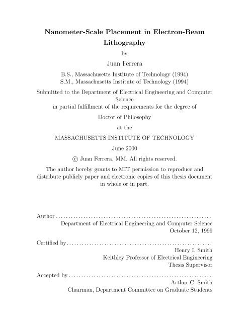
The pr<strong>in</strong>ciple of operation of the SEM is depicted <strong>in</strong> Fig. 1.2. Briefly, electrons are<br />
extracted from a source (usually a heated sharp tip). The electrons are accelerated to<br />
1 Other systems, based on the TEM, project a demagnified image of a maskor a shaped aperture<br />
onto the substrate. Mask-based systems promise high throughput through parallel exposure. For<br />
these tools, the masks are made us<strong>in</strong>g th<strong>in</strong> membranes because they must be transparent to electrons.<br />
These membranes tend to deform when subjected to high electron flux.
30 Introduction<br />
energies rang<strong>in</strong>g from 10 keV to 100 keV by bias<strong>in</strong>g the tip to the appropriate voltage<br />
with respect to an extraction electrode, which is grounded.<br />
F<strong>in</strong>al Lens<br />
Stepp<strong>in</strong>g<br />
Stage<br />
Substrate<br />
<strong>Electron</strong> Source<br />
Condenser Lenses<br />
Aperture<br />
-<br />
10-100 kV<br />
+<br />
Blank<strong>in</strong>g electrodes<br />
Deflection Coils<br />
Figure 1.2: Pr<strong>in</strong>ciple of operation of the scann<strong>in</strong>g-electron microscope: <strong>Electron</strong>s<br />
emitted from a heated tip are focused by a set of magnetic lenses to form a probe<br />
on the workpiece. The probe is scanned by transverse electric or magnetic fields.<br />
For lithography, the beam is turned off by a set of blank<strong>in</strong>g electrodes.<br />
A set of magnetic lenses forms a probe by project<strong>in</strong>g a demagnified image of the<br />
source on the surface of the sample. The amount of demagnification depends on the<br />
effective diameter of the source and the probe diameter desired. The probe is scanned<br />
across the surface by means of electric or magnetic fields, transverse to the trajectory<br />
of the electron beam.<br />
For lithography, a means to turn the beam on and off is necessary. This is imple-
1.1 Overview of electron beam lithography 31<br />
mented by add<strong>in</strong>g a set of blank<strong>in</strong>g electrodes, which produce an electric field that<br />
deflects the beam away from the axis of the column. An aperture stops the off-axis<br />
electrons.<br />
Dur<strong>in</strong>g the late 1950’s and early 1960’s, the SEM was further developed at Cam-<br />
bridge University [11, 12]. Application of these <strong>in</strong>struments to lithography was also <strong>in</strong>-<br />
vestigated: Research programs were <strong>in</strong>itiated at West<strong>in</strong>ghouse, IBM Research, Cam-<br />
bridge University, Texas Instruments, and Hughes Research [13, 14].<br />
To automate the pattern<strong>in</strong>g process, the beam deflection was controlled by pro-<br />
grammable digital computers. Registration between different lithographic levels was<br />
achieved by us<strong>in</strong>g the <strong>in</strong>strument <strong>in</strong> microscope mode, imag<strong>in</strong>g registration marks<br />
present on the substrate, and align<strong>in</strong>g the pattern to them.<br />
The electron beam was used to modify polymer resist films, as is done <strong>in</strong> pho-<br />
tolithography. Irradiation of the polymer modifies its dissolution <strong>in</strong> the appropriate<br />
developer solution. The first exposures were carried out us<strong>in</strong>g the photoresist com-<br />
pounds used by the <strong>in</strong>dustry at the time, but the resolution obta<strong>in</strong>ed was relatively<br />
poor. The use of poly(methyl methacrylate) (PMMA) as an electron resist, reported<br />
<strong>in</strong> 1968 [15], greatly improved the resolution.<br />
Substrates were also successfully patterned by “contam<strong>in</strong>ation”, which denotes<br />
the e-beam-<strong>in</strong>duced polymerization of residual organic contam<strong>in</strong>ants <strong>in</strong> the vacuum<br />
chamber [16]. This technique was able to achieve very high resolution, but the process<br />
was extremely slow and unreliable.<br />
The <strong>in</strong>itial objective of the various research efforts was to develop e-beam tools<br />
to replace photolithographic pr<strong>in</strong>ters on the manufactur<strong>in</strong>g floor, when the resolution<br />
limit of photolithography was reached [17]. One very significant shortcom<strong>in</strong>g of SEBL<br />
is its serial nature: the picture elements (pixels) that form the pattern are exposed<br />
one after the other. Increas<strong>in</strong>g the exposure rate of e-beam lithography has been<br />
one of the major priorities <strong>in</strong> the development of the technology. Even so, the low<br />
throughput of e-beam lithography is one of the reasons that it application <strong>in</strong> <strong>in</strong>dustrial
32Introduction<br />
production is limited to mask mak<strong>in</strong>g.<br />
1.1.2Pattern placement<br />
Although resolution is an important element of a lithographic technology, pattern<br />
placement is just as important. As mentioned above, <strong>in</strong> IC’s patterns must be placed<br />
with<strong>in</strong> a fraction of the m<strong>in</strong>imum resolvable feature. <strong>Electron</strong>-beam lithography has<br />
demonstrated resolution down to 10 nm, but the pattern placement accuracy of this<br />
technique does not match its resolution.<br />
In very general terms, the electron microscope’s lenses are <strong>in</strong>homogeneous electric<br />
or magnetic fields, which cause electron trajectories to converge towards a focal po<strong>in</strong>t.<br />
The fields have cyl<strong>in</strong>drical symmetry around the axis of the lens. In order to scan<br />
the beam it must be deflected away from the axis. Off-axis, electron lenses show<br />
aberrations, such as astigmatism, coma, and chromatic aberration. Because of these<br />
aberrations, as the beam is scanned across the surface, the shape of the probe can<br />
vary from the m<strong>in</strong>imum circular spot obta<strong>in</strong>ed on-axis. If the spot is not allowed to<br />
vary <strong>in</strong> shape by more than a fraction of the nom<strong>in</strong>al beam diameter, there is a limit<br />
on the maximum deflection possible [18, 19, 20].<br />
Initially, most efforts <strong>in</strong> SEBL were put <strong>in</strong>to design<strong>in</strong>g lenses with low aberration,<br />
which would allow formaximum possible deflection. At that time (<strong>in</strong> the 1960’s and<br />
70’s), the area covered by one <strong>in</strong>tegrated circuit was ∼ 1mm× 1 mm, which could be<br />
covered by one field. A device wafer could be put on a mechanical stage, which would<br />
position the substrate so that one chip was exposed at a time ( see Fig. 1.2). Overlay<br />
could be ensured by imag<strong>in</strong>g registration marks. The electromagnetic deflection of<br />
an e-beam is much fasterthan mechanical stage movements, so <strong>in</strong> orderto maximize<br />
the speed of writ<strong>in</strong>g, stage movement must be m<strong>in</strong>imized. This implies that the field<br />
should be made as large as possible.<br />
With careful eng<strong>in</strong>eer<strong>in</strong>g of electron optics and dynamic correction of the focus,<br />
astigmatism, and beam deflection, fields as large as 5 mm × 5 mm were exposed [21,
1.1 Overview of electron beam lithography 33<br />
22, 23] with a resolution of 0.5 µm and placement accuracy of 0.12 µm.<br />
Modern IC technology is evolv<strong>in</strong>g <strong>in</strong> the direction of sub-100 nm features over<br />
fields of 25 mm × 25 mm and larger. To write a l<strong>in</strong>ewidth of 100 nm, the beam<br />
diameter and pixel spac<strong>in</strong>g should be about 25 nm. (In order to have control over the<br />
exposed l<strong>in</strong>ewidth, the m<strong>in</strong>imum dimension is usually required to consist of at least<br />
4 resolvable elements [13].) Hence the full field consists of 10 6 × 10 6 pixels. There are<br />
at least two reasons why such a large field conta<strong>in</strong><strong>in</strong>g such a number of pixels cannot<br />
be exposed by e-beam lithography: limitations of electron optics; and limitations of<br />
beam-deflection electronics.<br />
In practice the field of view of an electron lens never exceeds about 5 mm. This<br />
is because <strong>in</strong> electron optics only simple converg<strong>in</strong>g lenses exist [24]. In contrast, <strong>in</strong><br />
light optics both diverg<strong>in</strong>g as well as converg<strong>in</strong>g lenses exist. In this case spherical<br />
aberration can be elim<strong>in</strong>ated by arrang<strong>in</strong>g the design so that the positive spherical<br />
aberration coefficient of the converg<strong>in</strong>g lens cancels the negative coefficient of the di-<br />
verg<strong>in</strong>g lens. This has allowed the field of view of light-optical systems to be <strong>in</strong>creased<br />
without sacrific<strong>in</strong>g their resolution.<br />
To expose a field with 10 6 × 10 6 addressable elements would require 20-bit digital-<br />
to-analog converters (with l<strong>in</strong>earity better than 20 bits) operat<strong>in</strong>g at pixel rates of 160<br />
MHz or more, <strong>in</strong> order to satisfy throughput requirements. The electronic amplifiers<br />
that drive the deflection system would require similar bandwidths and dynamic range.<br />
To the author’s knowledge, electronics that meet these requirements are not currently<br />
available.<br />
For the reasons stated above, <strong>in</strong>creas<strong>in</strong>g the field size of e-beam systems to cover<br />
the area of an entire IC was considered impractical and was abandoned.<br />
1.1.3 Field stitch<strong>in</strong>g<br />
An alternative approach was first developed <strong>in</strong> 1970 at Thomson CSF [25, 26]. The<br />
pattern was exposed as a mosaic of small fields (∼ 100-300 µm ). To ensure that the
34 Introduction<br />
fields were properly placed (so-called field stitch<strong>in</strong>g), the stage position was measured<br />
with two laser <strong>in</strong>terferometers, one for each axis of motion, as depicted <strong>in</strong> Fig. 1.3.<br />
The beams of the <strong>in</strong>terferometers were reflected off two orthogonal mirrors. The<br />
resolution of the <strong>in</strong>terferometers was λ/16, or ∼ 40 nm (HeNe laser), and a pattern-<br />
placement accuracy of 100 nm was achieved over a 5 cm x 5 cm area. This method has<br />
been almost universally adopted for high-accuracy lithography mach<strong>in</strong>es (<strong>in</strong>clud<strong>in</strong>g<br />
photolithography tools) [27]-[35] and position metrology <strong>in</strong>struments [36]-[39].<br />
computer<br />
fold mirror<br />
RS232 / GPIB<br />
laser<br />
fiber optic<br />
cable<br />
50 % beamsplitter<br />
fiber optic pickup<br />
"<strong>in</strong>terferometer"<br />
electronics<br />
two-axis<br />
stage mirror<br />
Figure 1.3: An <strong>in</strong>terferometrically controlled x-y stage uses two orthogonal plane<br />
mirrors as the references. Two Michelson <strong>in</strong>terferometers measure the displacement<br />
along each axis. Sub-wavelength precision is achieved by <strong>in</strong>terpolat<strong>in</strong>g between<br />
fr<strong>in</strong>ges.<br />
The <strong>in</strong>vention of the heterodyne <strong>in</strong>terferometer [40], made position measurement<br />
with a resolution of λ/128 ≈ 5 nm possible. Today, <strong>in</strong>struments with λ/2048 resolu-<br />
tion are available commercially 2<br />
2 from the Hewlett-Packard Company and Zygo Corp.
1.1 Overview of electron beam lithography 35<br />
When a lithography tool relies on field stitch<strong>in</strong>g, beam deflection and stage mo-<br />
tion must be exactly matched to prevent errors <strong>in</strong> feature placement. This can be<br />
accomplished by calibrat<strong>in</strong>g the deflection to stage motion. However, the exposure of<br />
a pattern cover<strong>in</strong>g an area of several square centimeters can take several hours; both<br />
subsystems have to stay matched throughout this period. In practice, despite strict<br />
control of the environment, the beam will drift with respect to the stage.<br />
From the discussion above, the contributions to pattern placement errors can be<br />
divided <strong>in</strong> two classes:<br />
1. Intrafield distortion: the distortion <strong>in</strong> beam position<strong>in</strong>g with<strong>in</strong> one field.<br />
2. Interfield distortion, the mismatch between two adjacent fields.<br />
Us<strong>in</strong>g this classification, the contributions to pattern placement can be more read-<br />
ily identified. Table 1.1 lists several contributors to pattern placement errors. Both<br />
classes of errors have static and dynamic sources. In pr<strong>in</strong>ciple, static sources of er-<br />
ror can be elim<strong>in</strong>ated by implement<strong>in</strong>g proper calibration procedures, but dynamic<br />
sources of error require the mach<strong>in</strong>e to be periodically recalibrated. The duration of<br />
calibration procedures can add prohibitive amounts of overhead to exposure times.<br />
Further, fast contributions, such as vibrations and stray electromagnetic fields, cannot<br />
be elim<strong>in</strong>ated.<br />
1.1.4 <strong>Beam</strong> scann<strong>in</strong>g strategies<br />
Each field can be thought of as a square array of pixels. In a serial exposure technique,<br />
such as SEBL, the <strong>in</strong>dividual pixels with<strong>in</strong> one field have to be exposed accord<strong>in</strong>g to<br />
a predeterm<strong>in</strong>ed sequence. The choice of exposure sequence can <strong>in</strong>fluence throughput<br />
and pattern placement. Two ma<strong>in</strong> strategies have been implemented [41]:<br />
1. Vectorscan: Foreach shape the beam is deflected to the location of the first<br />
pixel and unblanked. The pattern generator then deflects the beam to fill <strong>in</strong>
36 Introduction<br />
Table 1.1: Sources of pattern distortion.<br />
Intrafield errors<br />
Static Lens aberrations<br />
Deflection non-l<strong>in</strong>earity<br />
Dynamic Electrical charg<strong>in</strong>g of sample and e-beam system parts<br />
Stray magnetic fields, both static and dynamic<br />
Differential motions of the electron optics (vibrations, thermal)<br />
Interfield errors<br />
Static Mismatch of <strong>in</strong>terferometer and beam-deflection length scales<br />
Rotation of deflection axes relative to stage motion axes<br />
Non-flatness of stage mirrors<br />
Non-orthogonality of stage mirrors<br />
Non-rectil<strong>in</strong>ear stage motion<br />
Non-flatness of sample<br />
Dynamic Electrical charg<strong>in</strong>g of sample and e-beam system parts<br />
Stray magnetic fields<br />
Temperature changes<br />
Mechanical vibrations<br />
the rest of the pixels conta<strong>in</strong>ed with<strong>in</strong> the shape. The beam is then blanked<br />
and deflected to the next shape. In this way, only the pixels to be exposed are<br />
addressed.<br />
2. Raster scan: In this mode of operation, the beam addresses all pixel locations<br />
with<strong>in</strong> the array and is unblanked to expose a pixel. The pixels are addressed<br />
sequentially, start<strong>in</strong>g, for example, with the top row and deflect<strong>in</strong>g the beam<br />
left-to-right (see Fig. 1.4). Once all the pixels <strong>in</strong> the first row have been ad-<br />
dressed, the beam is deflected downwards, to the second row, and all pixels <strong>in</strong><br />
the row are addressed right-to-left. The process cont<strong>in</strong>ues until all the pixels<br />
with<strong>in</strong> the field have been addressed 3 .<br />
Vector scann<strong>in</strong>g is generally considered desirable if the area to be exposed is less<br />
than half the total area, s<strong>in</strong>ce only exposed pixels have to be addressed. However,<br />
3 This mode of scann<strong>in</strong>g is known as boustrophedonic, from the Greek boustrophedon, “follow<strong>in</strong>g<br />
the ox furrow”. A more common type of raster scan, used <strong>in</strong> cathode-ray-tube displays, is performed<br />
the same way as European writ<strong>in</strong>g, from left to right and from top to bottom [42].
1.1 Overview of electron beam lithography 37<br />
<strong>Beam</strong><br />
Blanker<br />
Deflector<br />
Stripe Stage movement<br />
Chip Chip<br />
Field<br />
(a) (b)<br />
Figure 1.4: Illustration of raster scan (a) and vector scan (b) methods.<br />
the beam settl<strong>in</strong>g time must be taken <strong>in</strong>to account; it can add significant overhead if<br />
the pixel address<strong>in</strong>g rate of the mach<strong>in</strong>e is high (> 20 MHz).<br />
On the other hand, the regularity of the raster technique allows for a simpler<br />
implementation. The EBES mach<strong>in</strong>e, <strong>in</strong>itially developed at Bell Laboratories [43], is a<br />
raster-scan tool. The fast, horizontal scann<strong>in</strong>g is done by electrostatic beam deflection<br />
on a 140 µm field, while the slow vertical scan is implemented by mov<strong>in</strong>g the sample<br />
stage under the beam at a constant rate. Small amounts of vertical deflection are<br />
necessary to compensate for the cont<strong>in</strong>uous motion of the stage. In this way, field<br />
boundaries are elim<strong>in</strong>ated <strong>in</strong> the vertical direction: the pattern across the substrate<br />
is subdivided <strong>in</strong> vertical stripes. At the end of each stripe the stage reverses direction<br />
vertically, horizontally steps to the next stripe, and the beam commences writ<strong>in</strong>g<br />
aga<strong>in</strong>. The stage position is monitored with laser <strong>in</strong>terferometers, and correction<br />
signals are applied to the beam deflection to compensate for stage errors. S<strong>in</strong>ce<br />
the beam is scanned <strong>in</strong> a very regular manner, and essentially along only one axis,
38 Introduction<br />
Table 1.2: Performance of the MEBES 4500S.<br />
lithographic performance<br />
write time (64 Mb DRAM) 140 m<strong>in</strong><br />
write scan l<strong>in</strong>earity 20 nm<br />
pattern position accuracy 40 nm<br />
resolution 0.2 µm<br />
l<strong>in</strong>ewidth control 35 nm<br />
l<strong>in</strong>ewidth uniformity 35 nm<br />
environment stability requirements<br />
column temperature 20-23 ± 0.1 o C<br />
electronics temperature 20-23 ± 0.5 o C<br />
deflection distortion correction can be implemented more effectively. The horizontal<br />
deflection signal is simply a sawtooth, and deviations from l<strong>in</strong>earity can be calibrated<br />
out. Blank<strong>in</strong>g tim<strong>in</strong>g determ<strong>in</strong>es which pixels are exposed. High pixel exposure rates<br />
can be achieved by implement<strong>in</strong>g a fast blanker. 4<br />
1.1.5 Pattern placement performance of modern tools<br />
The performance specifications of a MEBES 4500 electron-beam mask maker are<br />
listed <strong>in</strong> table 1.2.<br />
Compared with the first e-beam mach<strong>in</strong>es, implemented <strong>in</strong> the 1970’s, the specifi-<br />
cations for this mach<strong>in</strong>e show very significant improvements <strong>in</strong> both the throughput<br />
and the data handl<strong>in</strong>g capacity of the control computer, which make possible the<br />
exposure of complex patterns <strong>in</strong> a few hours. However, there is only moderate im-<br />
provement <strong>in</strong> resolution and pattern placement errors.<br />
In today’s semiconductor <strong>in</strong>dustry, virtually all lithography is done by optical<br />
projection of a mask onto the substrate, s<strong>in</strong>ce this proven technology has advanced<br />
enough to meet the resolution and manufactur<strong>in</strong>g requirements. Although e-beam<br />
4The MEBES tools, succesors of the EBES, have pixel exposure rates of up to 160 MHz [44, 45,<br />
46, 47, 48, 49].
1.2The global fiducial grid 39<br />
lithography does not meet the throughput requirements, it is nonetheless of crucial<br />
importance <strong>in</strong> mask mak<strong>in</strong>g [44]. No other mask pattern<strong>in</strong>g technique can match the<br />
resolution of electron beams, and all masks for the most advanced device generations<br />
are patterned <strong>in</strong> this way. Patterns cannot be directly registered to substrate marks<br />
when perform<strong>in</strong>g lithography on masks, s<strong>in</strong>ce all pattern<strong>in</strong>g is done on a blank sub-<br />
strate. Instead, placement errors are decreased by imag<strong>in</strong>g a fiducial mark on the<br />
stage, away from the writ<strong>in</strong>g area. This operation is time consum<strong>in</strong>g and is there-<br />
fore performed <strong>in</strong>frequently. The system must run open-loop between registration<br />
operations.<br />
The SemiconductorIndustry Association, <strong>in</strong> its 1997 Technology Roadmap for<br />
Semiconductors, lists estimates for lithographic pattern placement accuracy and me-<br />
trology requirements for future <strong>in</strong>tegrated circuit generations, characterized by the<br />
m<strong>in</strong>imum feature size (critical dimension). (See table 1.3.) It is estimated that<br />
conventional technology will not yield the pattern overlay required for the 70 nm<br />
generation (<strong>in</strong> the year 2009). This document states that [50]:<br />
Overlay and CD [critical dimension] improvements have not kept pace<br />
with resolution improvements. The estimates for overlay appear to plateau<br />
around 30 nm. This will be <strong>in</strong>adequate for ground rules less than 100<br />
nm. Overlay and CD control over large field sizes cont<strong>in</strong>ue to be a major<br />
concern from sub-130 nm lithography.<br />
Lithographic tools may have to rely on a different method to correct feature place-<br />
ment errors. Indirect referenc<strong>in</strong>g has worked well for 30 years, but may have to be<br />
replaced with a direct reference scheme.<br />
1.2The global fiducial grid<br />
The <strong>in</strong>terference of two mutually coherent laser beams has been used for several years<br />
to produce high-quality diffraction grat<strong>in</strong>gs. To provide adequate performance <strong>in</strong>
40 Introduction<br />
Table 1.3: Predicted lithography requirements. (From [51])<br />
Year of First Product Shipment<br />
Technology Generation<br />
1997<br />
250 nm<br />
1999<br />
180 nm<br />
2001<br />
150 nm<br />
2003<br />
130 nm<br />
2006<br />
100 nm<br />
2009<br />
70 nm<br />
Gate CD control (nm) 20 14 12 10 7 5 4<br />
F<strong>in</strong>al CD output metrology precision<br />
(nm, 3 sigma) *<br />
4 3 2 2 1.4 1 0.8<br />
Overlay control (nm) 85 65 55 45 35 25 20<br />
Overlay output metrology precision<br />
(nm, 3 sigma)*<br />
9 7 6 5 4 3 2<br />
Solutions Exist Solutions Be<strong>in</strong>g Pursued No Known Solution<br />
* Measurement tool performance needs to be <strong>in</strong>dependent of l<strong>in</strong>e shape, l<strong>in</strong>e materials, and density of l<strong>in</strong>es<br />
2012<br />
50 nm<br />
spectroscopy apparatus, the l<strong>in</strong>es that comprise the grat<strong>in</strong>gs must be spaced with<br />
great regularity (a very small fraction of the grat<strong>in</strong>g period).<br />
The application of grat<strong>in</strong>gs produced with <strong>in</strong>terference lithography as metrological<br />
standards follows from their regularity, or to use a different expression, from their<br />
spatial-phase coherence.<br />
Smith et al. [52] recognized that structures fabricated by <strong>in</strong>terference lithography<br />
could, due to their coherence, be used as metrological standards. They addressed the<br />
problem of <strong>in</strong>tra-field distortion. They used a grid (made by pattern<strong>in</strong>g two grat<strong>in</strong>gs at<br />
a right angle to one another) to measure the deflection field of a vector-scan electron-<br />
beam tool. Anderson et al. [53] performed similar measurements. As a result of these<br />
measurements, they found that most of the distortion was caused by non-l<strong>in</strong>earities of<br />
the digital-to-analog (D/A) converters used to generate beam deflection signals. They<br />
also found that <strong>in</strong>creas<strong>in</strong>g the field size beyond 100 µm caused distortion <strong>in</strong>duced by<br />
electron-optical aberrations. Hav<strong>in</strong>g quantified the magnitude of the distortion, they<br />
corrected it by calibrat<strong>in</strong>g the D/A converters. <strong>Electron</strong>-optical distortion was not<br />
corrected because it is negligible if field sizes ≤ 100 µm are used. If larger field sizes<br />
are desired, it is relatively straightforward to implement calibration tables to remove<br />
non-l<strong>in</strong>earities <strong>in</strong> the deflection field. Us<strong>in</strong>g this approach, it is possible to elim<strong>in</strong>ate<br />
<strong>in</strong>tra-field distortion, but <strong>in</strong>ter-field distortion, due to drift, still rema<strong>in</strong>s.<br />
Smith et al. [54] applied the use if IL-generated grids to the correction of <strong>in</strong>terfield
1.2The global fiducial grid 41<br />
distortion. They proposed to reference the beam position directly to a global fiducial<br />
grid placed on the substrate. This scheme makes it possible to measure beam position<br />
on the sample, without rely<strong>in</strong>g on <strong>in</strong>termediate variables, such as the position of the<br />
sample stage. In other words, the global fiducial grid on the sample becomes the<br />
metrological standard of the lithography tool, replac<strong>in</strong>g the <strong>in</strong>terferometer-controlled<br />
stage. The grid is a periodic structure, so that a spatial phase can be assigned to<br />
it. This will be described <strong>in</strong> more detail <strong>in</strong> a later section. S<strong>in</strong>ce <strong>in</strong> this scheme the<br />
patterns are placed with respect to the grid, it can be said that they are “locked” to<br />
its spatial phase. Hence, the method proposed by Smith et al. is called Spatial-Phase-<br />
Locked <strong>Electron</strong>-<strong>Beam</strong> <strong>Lithography</strong> (SPLEBL).<br />
A version of the scheme is depicted <strong>in</strong> Fig. 1.5. Ideally, the grid consists of an<br />
array of features placed at regular <strong>in</strong>tervals on the surface of the workpiece. As<br />
the electron beam is scanned, a time-vary<strong>in</strong>g signal is collected, such as secondary<br />
electrons, photons, etc. The collected signal changes when the beam is placed on<br />
one of the features. Thus, the signal is modulated by the position of the beam on<br />
the substrate. If the position of the nodes is known one can <strong>in</strong>fer the beam position<br />
from the collected signal, and any deviations <strong>in</strong> the beam’s position can be corrected<br />
concurrently with exposure.<br />
The fiducial grid, like the <strong>in</strong>terferometer stage, relies on the <strong>in</strong>terference of coherent<br />
light waves for distance metrology. There is an important difference, however: the<br />
physical grid is part of the workpiece and is therefore a time-<strong>in</strong>variant reference, while<br />
the virtual grid of the <strong>in</strong>terferometer stage is not directly l<strong>in</strong>ked to the sample, and<br />
is subject to drift. Moreover, sample distortion caused by clamp<strong>in</strong>g <strong>in</strong> the SEBL tool<br />
or temperature effects, will affect the grid <strong>in</strong> the same way. S<strong>in</strong>ce SPLEBL references<br />
pattern placement to the grid, sample distortion should no affect pattern placement.<br />
The use of a periodic fiducial implies that position measurement is ambiguous<br />
to one half of the period, so the lithography mach<strong>in</strong>e must be accurate enough to<br />
remove this ambiguity. If the period of the fiducial grid is 200 nm, then the pattern<br />
placement accuracy of the stage by itself must be better than 100 nm. For this, it is
42Introduction<br />
Λ<br />
h<br />
e-beam<br />
fiducial<br />
grid<br />
resist<br />
substrate<br />
SE Detector<br />
photon<br />
Λ < 2 µm<br />
h < 50 nm<br />
v<br />
written<br />
pattern<br />
grid<br />
signal<br />
Figure 1.5: Conceptual depiction of a direct referenc<strong>in</strong>g scheme for SEBL mach<strong>in</strong>es,<br />
denom<strong>in</strong>ated spatial-phase-locked electron-beam lithography (SPLEBL). A<br />
fiducial grid is placed directly on the substrate surface. It is <strong>in</strong>tended to <strong>in</strong>teract<br />
with the electron beam and produce a signal, which is collected by a detector. The<br />
position of the beam relative to the grid is encoded <strong>in</strong> this signal.<br />
simplest to rely on an <strong>in</strong>terferometer stage, but this is not required.<br />
When the sample stage steps to a new field, the residual error of the beam position<br />
on the sample is unknown, and can only be corrected once the beam has started<br />
scann<strong>in</strong>g the sample. To pre-align the field, the grid must be sampled at very low dose,<br />
caus<strong>in</strong>g no resist exposure. After the pre-alignment step, exposure can commence and<br />
cont<strong>in</strong>uous feedback is then possible.<br />
The concept of the global fiducial grid opened a vast area of <strong>in</strong>vestigation. Sub-<br />
sequent work demonstrated the feasibility of the technique, but many issues need to<br />
t
1.3 The segmented grid 43<br />
be resolved before applications outside of the research laboratory can be considered.<br />
The open areas of research are summarized <strong>in</strong> Table 1.4.<br />
1. Measurement of grid fidelity<br />
2. Optimization of signal type<br />
Table 1.4: Research areas<br />
(a) Choice of electron-beam generated signal<br />
(b) Grid material<br />
• Must provide adequate signal<br />
• Must not <strong>in</strong>troduce artifacts <strong>in</strong>to the patterns be<strong>in</strong>g written (such as<br />
l<strong>in</strong>e broaden<strong>in</strong>g due to beam scatter<strong>in</strong>g)<br />
• Must be easily stripped before development, without affect<strong>in</strong>g resist<br />
(c) Grid fabrication process must be simple and reliable<br />
3. Optimization of signal-detector parameters: collection angle, frequency response,<br />
ga<strong>in</strong>, etc.<br />
4. Signal process<strong>in</strong>g to extract beam position <strong>in</strong>formation from detected signal,<br />
and remove noise<br />
5. Optimization of beam scann<strong>in</strong>g strategy, to ensure that position <strong>in</strong>formation<br />
for both directions is effectively acquired<br />
6. Applications of SPLEBL<br />
1.3 The segmented grid<br />
One fundamental constra<strong>in</strong>t <strong>in</strong> the implementation of a SPLEBL tool is that acqui-<br />
sition of the signal must not <strong>in</strong>terfere with the pattern<strong>in</strong>g of features. However, to<br />
obta<strong>in</strong> a signal from the fiducial grid, it is necessary to irradiate it, which will expose<br />
the resist if the dose is high enough. The SPLEBL process must be designed so that<br />
an adequate signal can be obta<strong>in</strong>ed without unwanted exposure of the resist.<br />
A second constra<strong>in</strong>t relates to the implementation of the feedback loop. It is neces-
44 Introduction<br />
sary to know the time constants and magnitudes of the different sources of <strong>in</strong>terference<br />
with<strong>in</strong> the e-beam tool. From Table 1.1, these <strong>in</strong>clude drift terms (with long time<br />
constants), such as charg<strong>in</strong>g <strong>in</strong> the column; thermally <strong>in</strong>duced expansion/contraction<br />
of the different mechanical components; and thermal drift of the electronics that focus<br />
and deflect the beam.<br />
Fast (short time constant) <strong>in</strong>terference <strong>in</strong>cludes vibrations <strong>in</strong> the mechanical com-<br />
ponents, as well as 60 Hz and RF electromagnetic <strong>in</strong>terference. (RF <strong>in</strong>terference can<br />
be elim<strong>in</strong>ated by proper use of shield<strong>in</strong>g and electrical filter<strong>in</strong>g.) Once the sources<br />
of <strong>in</strong>terference are known, a feedback loop can be designed to lock the beam to the<br />
substrate below a specified tolerance.<br />
Figure 1.6 (a) depicts the most general implementation of SPLEBL. The fiducial<br />
grid is present throughout the surface of the substrate, and patterns may be exposed<br />
anywhere on the surface. This implies that the grid may not disturb the lithographic<br />
exposure — the signal must either be collected while patterns are be<strong>in</strong>g exposed, or<br />
collected prior to exposure, but at such a low dose that the resist is not exposed.<br />
Dynamically, <strong>in</strong>terference must be elim<strong>in</strong>ated up to frequencies of several hundred<br />
Hertz, so that real-time signal process<strong>in</strong>g is required. These requirements make the<br />
implementation of the feedback loop quite challeng<strong>in</strong>g.<br />
In applications where patterns need not be exposed at all locations on the sub-<br />
strate, areas for the fiducial can be allocated which are separate from areas where the<br />
lithography is to be performed. It is then possible to relax some of the requirements<br />
outl<strong>in</strong>ed <strong>in</strong> the previous section, thus significantly simplify<strong>in</strong>g the implementation of<br />
a SPLEBL system, which is nonetheless quite useful for some applications. Ferrera<br />
et al. [55, 56] proposed and implemented such a scheme, the segmented fiducial grid<br />
(illustrated <strong>in</strong> Fig. 1.6 (b)).<br />
The areas conta<strong>in</strong><strong>in</strong>g the fiducial grid can be small (e.g. 0.1% of the total sample<br />
area). If such a compromise is made, the fiducial can be sampled for long periods<br />
of time to obta<strong>in</strong> an adequate signal, and lock<strong>in</strong>g to the grid can be done with high
1.3 The segmented grid 45<br />
fiducial grid pattern<br />
( 0, 0 )<br />
fiducial grid<br />
(a) (b)<br />
Figure 1.6: (a) The global grid: reference nodes are present everywhere on the<br />
substrate surface. Patterns may be written at any location on the sample. (b)<br />
The segmented grid, a simplification of the global grid concept: reference nodes<br />
are present with<strong>in</strong> small areas allocated for them. Patterns may be written at any<br />
location, except the reference areas.<br />
precision.<br />
( 0, 0 )<br />
pattern<br />
area<br />
The segmented-grid approach assumes that the SEBL system is stable for short<br />
time scales (< 1 s — the typical writ<strong>in</strong>g time for a s<strong>in</strong>gle field), so that sampl<strong>in</strong>g of<br />
the grid does not have to occur concurrently with writ<strong>in</strong>g. This elim<strong>in</strong>ates the need<br />
for real-time signal process<strong>in</strong>g.<br />
In addition, the deflection of the beam with<strong>in</strong> one field must meet the pattern<br />
placement requirements.<br />
The implementation of a segmented-grid scheme was motivated by the need to<br />
fabricate Bragg grat<strong>in</strong>gs for a variety of <strong>in</strong>tegrated optical devices. In such devices,<br />
a grat<strong>in</strong>g with feature sizes on the order of 100 nm is patterned on an optical waveg-<br />
uide. The grat<strong>in</strong>g is up to several millimeters long, and each one of the l<strong>in</strong>es that<br />
comprise it must be positioned with<strong>in</strong> 5 nm. Such fabrication is beyond the capabil-<br />
ities of a conventional lithography system, but was carried out successfully us<strong>in</strong>g a<br />
1-D segmented fiducial-grid scheme.
46 Introduction<br />
The work reported <strong>in</strong> this document is not <strong>in</strong>tended to address all of the issues<br />
listed <strong>in</strong> Table 1.4. It is restricted to two ma<strong>in</strong> avenues of research:<br />
1. The characterization of grids exposed by <strong>in</strong>terference lithography<br />
2. The application of the segmented-grid scheme to the fabrication of <strong>in</strong>tegrated<br />
optical devices<br />
Chapter 2 describes the <strong>in</strong>terference lithography apparatus used to fabricate fidu-<br />
cial grids. This apparatus uses the <strong>in</strong>terference of two diverg<strong>in</strong>g optical waves, which<br />
emanate from two spatial filters, to produce high-fidelity grat<strong>in</strong>gs. The use of diverg-<br />
<strong>in</strong>g waves implies that the spac<strong>in</strong>g between the grat<strong>in</strong>g l<strong>in</strong>es is not uniform throughout<br />
the substrate, i.e., the grat<strong>in</strong>g is non-l<strong>in</strong>ear. Chapters 3 and 4 develop a model to<br />
predict the feature locations of a grid recorded by <strong>in</strong>terference lithography. Grids are<br />
made by expos<strong>in</strong>g two grat<strong>in</strong>gs at right angles to one another, so that the analysis of<br />
grat<strong>in</strong>gs can also be applied to grids. A model is proposed, which assumes that spher-<br />
ical wavefronts <strong>in</strong>terfere at the substrate plane to form the grat<strong>in</strong>g image. Chapter 3<br />
presents an argument to support this assumption, based on scalar diffraction the-<br />
ory and the Fraunhofer far-field approximation. Measurements of far-field <strong>in</strong>tensity<br />
patterns are reported, which <strong>in</strong>dicate that the proposed model is valid <strong>in</strong> describ<strong>in</strong>g<br />
the operation of the <strong>in</strong>terference lithography apparatus. The spherical-wave model<br />
is used <strong>in</strong> Chapter 4 to develop a model, which predicts the feature locations of a<br />
grat<strong>in</strong>g recorded by <strong>in</strong>terference lithography. The model is used to estimate grat<strong>in</strong>g<br />
distortion <strong>in</strong>duced by substrate non-flatness, mount<strong>in</strong>g errors, and the uncerta<strong>in</strong>ty<br />
<strong>in</strong> determ<strong>in</strong><strong>in</strong>g the distance and angle between the po<strong>in</strong>t sources and the substrate<br />
surface. Chapter 5 describes several methods to measure the characteristics of <strong>in</strong>ter-<br />
ferometric grat<strong>in</strong>gs and reports the experimental results. The experimental results<br />
are found to agree well with the model of Chapter 4.<br />
Subsequent chapters report the implementation of a segmented-grid scheme on an<br />
SEBL system, and its application <strong>in</strong> the fabrication of Bragg-grat<strong>in</strong>g based optical<br />
devices. Chapter 6 briefly describes the pr<strong>in</strong>ciple of operation of a Bragg-grat<strong>in</strong>g based
1.3 The segmented grid 47<br />
device: the <strong>in</strong>tegrated channel-dropp<strong>in</strong>g filter. A stochastic model is used to evaluate<br />
the impact of pattern-placement errors on device performance. The implementation<br />
of the segmented grid algorithm, which is covered <strong>in</strong> detail <strong>in</strong> the author’s M.S.<br />
thesis, is briefly reviewed. The use of SPLEBL <strong>in</strong> generat<strong>in</strong>g Bragg-grat<strong>in</strong>g patterns<br />
is reported, and the quality of these grat<strong>in</strong>gs is evaluated. This chapter also describes<br />
the process used to fabricate λ/4-shifted resonators on waveguides and reports the<br />
measured device performance. Chapter 7 describes further ref<strong>in</strong>ements made to the<br />
segmented grid scheme. Chapter 8 reports the development of a process to fabricate a<br />
second generation of optical devices. Several problems found dur<strong>in</strong>g the fabrication of<br />
the first device generation are addressed. Chapter 9 concludes with a brief summary.
Chapter 2<br />
Interference lithography<br />
Thomas Young’s famous experiment was the first demonstration of the <strong>in</strong>terference<br />
of light [57]. The experiment is set-up as follows: light from a monochromatic po<strong>in</strong>t<br />
source illum<strong>in</strong>ates two p<strong>in</strong>holes located very close together on a screen. The p<strong>in</strong>-<br />
holes act as secondary po<strong>in</strong>t sources. The light beams that emanate from them are<br />
projected onto a screen, placed at a distance significantly larger than the separation<br />
between the p<strong>in</strong>holes. In the region where the two beams overlap a pattern of bright<br />
and dark bands appears. These bands are called <strong>in</strong>terference fr<strong>in</strong>ges. As the angle<br />
of <strong>in</strong>terference of the two beams is <strong>in</strong>creased, the fr<strong>in</strong>ges quickly become microscopic.<br />
Albert Michelson suggested record<strong>in</strong>g the <strong>in</strong>terference fr<strong>in</strong>ges produced by such an ar-<br />
rangement on Lippmann photographic plates [58], to improve on the quality of ruled<br />
grat<strong>in</strong>gs for spectroscopy.<br />
Today, <strong>in</strong>terference lithography (IL) is widely used to produce periodic structures.<br />
The modern apparatus used for <strong>in</strong>terference lithography is <strong>in</strong> pr<strong>in</strong>ciple no different<br />
from Young’s <strong>in</strong>terference experiment, although significant technological advances<br />
have been made, which enable the repeatable fabrication of well-characterized periodic<br />
structures over large areas. Until the <strong>in</strong>vention of the laser it was not possible to<br />
perform <strong>in</strong>terferometric exposures over large areas. Rudolph and Schmahl used light<br />
from a high-power laser to expose photoresist films, and were able to fabricate high-<br />
49
50 Interference lithography<br />
quality grat<strong>in</strong>gs for high resolution spectroscopy [59, 60].<br />
Interference lithography has been under development at MIT for over 25 years,<br />
at the Nanostructures Laboratory and the <strong>Space</strong> Microstructures Laboratory [52]-<br />
[70]. Patterns produced by this technique have been successfully used <strong>in</strong> a variety of<br />
applications, such as x-ray spectroscopy [71]-[73], epitaxial growth [74], atom-beam<br />
diffraction [75]-[77] and filter<strong>in</strong>g [78], x-ray mask distortion measurements [79, 80],<br />
and fabrication of optoelectronic devices [81]-[84]. These applications require grat<strong>in</strong>gs<br />
of high fidelity, i. e., the grat<strong>in</strong>gs’ l<strong>in</strong>es must not deviate from their ideal position by<br />
more than a small fraction of their period.<br />
The MIT IL system, now located <strong>in</strong> the <strong>Space</strong> Microstructures Laboratory, is<br />
specifically designed to produce grat<strong>in</strong>gs with m<strong>in</strong>imum amounts of distortion. The<br />
current system is the product of numerous contributions by a large number of people<br />
over several years [52]-[66]. For the work reported <strong>in</strong> this document, the system was<br />
used <strong>in</strong> its current configuration — no modifications were made to the apparatus,<br />
except to implement phase-shift<strong>in</strong>g measurements, as described <strong>in</strong> Chapter 4. The<br />
apparatus is described <strong>in</strong> this chapter, with emphasis on the various factors that affect<br />
the repeatability and accuracy of the grat<strong>in</strong>gs. Although it is known that grat<strong>in</strong>gs<br />
with very small distortions have been fabricated with this apparatus, the amount of<br />
distortion has not been quantified to the nanometer level.<br />
Subsequent chapters present a study of the fidelity of grat<strong>in</strong>gs fabricated by <strong>in</strong>-<br />
terference lithography, with reference to their application as metrological standards<br />
<strong>in</strong> spatial-phase-locked electron-beam lithography (SPLEBL). The aim of SPLEBL is<br />
to improve the pattern placement accuracy of e-beam tools beyond the limits found<br />
<strong>in</strong> today’s equipment, i.e., an accuracy better than 30 nm (mean + 3σ) over∼ 10<br />
cm diameter substrates. As described <strong>in</strong> the previous chapter, a global fiducial grid<br />
is patterned on the substrate surface by <strong>in</strong>terference lithography. The position of the<br />
beam is measured with respect to this grid, and any errors are corrected. Thus, <strong>in</strong><br />
SPLEBL, the grid is the ma<strong>in</strong> metrological reference for the whole system.<br />
In an error-budget analysis for SPLEBL, residual pattern-placement errors are
2.1 Description of the MIT apparatus 51<br />
assumed to be caused by two factors: distortions of the fiducial grid, and errors<br />
made by the SPLEBL system <strong>in</strong> lock<strong>in</strong>g the beam position to the grid. The grid’s<br />
fidelity must be guaranteed to be significantly better than the maximum error allowed.<br />
Although the fiducial grid’s accuracy requirements cannot be explicitly stated until an<br />
exhaustive analysis of the e-beam tool’s pattern placement specifications and sources<br />
of error has been carried out, it is a reasonable estimate that the tool’s metrology<br />
standard must be accurate to 1/10 of the pattern placement specification. That is, for<br />
a total error specification of 30 nm (mean + 3σ), grid distortion, when the substrate<br />
is unstra<strong>in</strong>ed, 1 must be guaranteed to be less than 3 nm over its entire area.<br />
2.1 Description of the MIT apparatus<br />
Figure 2.1 is a schematic diagram of the MIT <strong>in</strong>terference lithography (IL) apparatus.<br />
The light source is an argon-ion laser. It emits a beam of l<strong>in</strong>early polarized light with<br />
wavelength λ = 351.1 nm. The primary beam is divided by a dielectric beamsplitter<br />
<strong>in</strong>to two secondary beams or arms, each carry<strong>in</strong>g 50% of the total power. The two<br />
beams separate and are directed by mirrors towards two spatial filters.<br />
The spatial filters elim<strong>in</strong>ate any unwanted scattered light and coherent radiation<br />
other than the fundamental Gaussian mode of the laser cavity, to produce two “pure”<br />
diverg<strong>in</strong>g wavefronts, which imp<strong>in</strong>ge on the substrate at an angle and produce <strong>in</strong>ter-<br />
ference fr<strong>in</strong>ges. To ensure the fidelity of the grat<strong>in</strong>g, it is necessary to ensure that<br />
only the wavefronts emanat<strong>in</strong>g from the spatial filters are contribut<strong>in</strong>g to the stand<strong>in</strong>g<br />
wave at the substrate. Due to the long coherence length of the radiation used, any<br />
light scattered by the optic components or the table will coherently <strong>in</strong>terfere, result-<br />
<strong>in</strong>g <strong>in</strong> grat<strong>in</strong>g distortion. The additional <strong>in</strong>formation <strong>in</strong> the hologram is encoded as<br />
phase modulation of the <strong>in</strong>terference fr<strong>in</strong>ges. For this reason, the space between the<br />
1 Once the grid has been exposed on the substrate surface, any mechanical changes <strong>in</strong>troduced by<br />
temperature changes, clamp<strong>in</strong>g, etc. do not contribute to pattern distortion, s<strong>in</strong>ce the grid is rigidly<br />
attached to the substrate. Conversely, it must be ensured that the substrate is unstra<strong>in</strong>ed when the<br />
fiducial grid is exposed.
52Interference lithography<br />
a)<br />
mirror<br />
b)<br />
variable<br />
attenuator<br />
beamsplitter<br />
p = λ<br />
2 s<strong>in</strong>θ<br />
beamsplitter<br />
λ = 351 nm<br />
Resist<br />
ARC<br />
Substrate<br />
1) Exposure<br />
spatial filters<br />
2θ<br />
laser beam<br />
λ = 351.1 nm<br />
Pockels cell<br />
substrate<br />
phase error<br />
sensor<br />
Substrate<br />
2) Development<br />
Figure 2.1: (a) Schematic diagram of the MIT <strong>in</strong>terference lithography setup.<br />
(b) Detail of the <strong>in</strong>terference-lithographic process.<br />
spatial filters and the substrate is enclosed by non-reflect<strong>in</strong>g barriers to prevent any<br />
scattered light from reach<strong>in</strong>g the substrate.<br />
When <strong>in</strong>terfer<strong>in</strong>g two optical waves to record grat<strong>in</strong>gs, one would ideally use plane<br />
waves <strong>in</strong> order to produce a grat<strong>in</strong>g with a l<strong>in</strong>ear phase progression — a grat<strong>in</strong>g of<br />
straight, parallel and equidistant l<strong>in</strong>es. However, it is questionable whether truly<br />
plane waves, free of unpredictable errors at the nanometer level, can be produced with<br />
conventional apparatus. In order to have plane waves <strong>in</strong>cident on the substrate, one<br />
would use collimat<strong>in</strong>g lenses between the spatial filters and the substrate. However,<br />
figure errors <strong>in</strong> the lenses cause deviations from plane waves. The required lenses,<br />
with diameters of several centimeters and phase errors of only a few nanometers are<br />
ARC<br />
mirror
2.1 Description of the MIT apparatus 53<br />
either currently unavailable, or prohibitively expensive. Moreover, defects <strong>in</strong> the lens<br />
material, or dust particles on the lens surface will scatter light, creat<strong>in</strong>g spurious<br />
wavefronts. As a consequence of research be<strong>in</strong>g performed on extreme ultra-violet<br />
(EUV) lithography, reflectors with figure specifications <strong>in</strong> the nanometer range and<br />
surfaces free of defects might be available <strong>in</strong> the future. It might then become feasible<br />
to fabricate l<strong>in</strong>ear-phase grat<strong>in</strong>gs with deviations from perfect l<strong>in</strong>earity <strong>in</strong> the 1 nm<br />
range. The system would have to be eng<strong>in</strong>eered to prevent particles from settl<strong>in</strong>g<br />
on the reflect<strong>in</strong>g surfaces, a problem which is avoided <strong>in</strong> the MIT system by us<strong>in</strong>g<br />
diverg<strong>in</strong>g waves and hav<strong>in</strong>g no optics between the spatial filter and the substrate.<br />
The <strong>in</strong>terference pattern is recorded <strong>in</strong> a photoresist film that covers the substrate.<br />
The substrate is typically reflective, so that the additional unwanted wavefronts arise<br />
from reflection at the resist-substrate boundary. To attenuate these reflections an<br />
absorb<strong>in</strong>g anti-reflection coat<strong>in</strong>g (ARC) is applied to the substrate surface before the<br />
resist layer. The refractive <strong>in</strong>dex and thickness of the ARC designed to m<strong>in</strong>imize<br />
substrate reflection [85, 86].<br />
The periodicity of the fr<strong>in</strong>ges is determ<strong>in</strong>ed by the wavelength and the angle of<br />
<strong>in</strong>terference. The spatial filters are positioned so that straight l<strong>in</strong>es connect<strong>in</strong>g them<br />
to the centerof the substrate enclose an angle 2θ. Theperiodp of the fr<strong>in</strong>ges at the<br />
centerof the substrate is then given by<br />
p = λ<br />
2s<strong>in</strong>θ<br />
. (2.1)<br />
The system can be set up to expose grat<strong>in</strong>gs rang<strong>in</strong>g <strong>in</strong> period from 200 nm to<br />
approximately 4 µm. The period of the exposure is selected as follows: the spatial<br />
filters are removed from the setup, and the steer<strong>in</strong>g mirrors that direct the secondary<br />
beams towards the substrate are adjusted so that the beams imp<strong>in</strong>ge on the substrate<br />
at a desired angle θ with respect to the substrate surface normal. The angle is<br />
measured by means of a special assembly, which consists of a mirror mounted on a<br />
goniometer. The mirror is rotated by ±θ (see Fig. 2.2). The steer<strong>in</strong>g mirrors are
54 Interference lithography<br />
adjusted until the beam retroreflects off the goniometer mirror. This procedure is<br />
carried out for both beams. Then, the spatial filters are aligned to both beams.<br />
steer<strong>in</strong>g<br />
mirror<br />
θ<br />
beam beam<br />
goniometer<br />
mirror<br />
substrate<br />
normal<br />
spatial<br />
filter<br />
(a) (b)<br />
substrate<br />
normal<br />
substrate<br />
Figure 2.2: Schematic of the procedure used to adjust the angle of <strong>in</strong>cidence of the<br />
secondary beams. (a) The steer<strong>in</strong>g mirror is adjusted until the beam retroreflects<br />
on a mirror, which has been turned by θ. (b) The spatial filter is aligned to the<br />
beam.<br />
The use of diverg<strong>in</strong>g waves implies that the angle of <strong>in</strong>terference varies as a func-<br />
tion of position on the substrate. As a result, the period of the grat<strong>in</strong>g changes as a<br />
function of position on the substrate surface as well. Equation 2.1 will be extended<br />
<strong>in</strong> a latersection to <strong>in</strong>clude this effect.<br />
The two <strong>in</strong>terfer<strong>in</strong>g wavefronts must be equal <strong>in</strong> <strong>in</strong>tensity to achieve maximum<br />
contrast <strong>in</strong> the <strong>in</strong>terference pattern (perfect destructive <strong>in</strong>terference at the nulls). To<br />
this end, a variable attenuator (see Fig. 2.1) is placed <strong>in</strong> one of the secondary beams,<br />
so that the power<strong>in</strong> that beam can be f<strong>in</strong>e-tuned to match the power<strong>in</strong> the other.<br />
To m<strong>in</strong>imize particle defects dur<strong>in</strong>g grat<strong>in</strong>g exposure, the IL system is located<br />
<strong>in</strong> a cleanroom environment. In this environment the air is constantly be<strong>in</strong>g passed<br />
through filters to remove particulates. The consequences are turbulent air flow and<br />
acoustic vibrations, which disturb the optical components and cause dynamic optical<br />
path variations. After splitt<strong>in</strong>g the primary beam, the secondary beams traverse<br />
paths of approximately 3 meters before be<strong>in</strong>g recomb<strong>in</strong>ed, and the effective length of<br />
each arm may change by several wavelengths <strong>in</strong> a fraction of a second. Optical path<br />
variations directly <strong>in</strong>fluence the position of the <strong>in</strong>terference pattern. If the <strong>in</strong>terference<br />
pattern is not stationary over the ∼ 10 − 30 seconds necessary for resist exposure,
2.2 Laser specifications 55<br />
the result is an exposure with very poor contrast. A feedback system, depicted <strong>in</strong><br />
Fig. 2.1, measures the optical path difference between the two arms of the system<br />
and modulates the phase of one of the arms to keep the <strong>in</strong>terference pattern static <strong>in</strong><br />
space.<br />
The follow<strong>in</strong>g factors are important for grat<strong>in</strong>g fidelity and repeatability: laser<br />
wavelength, quality of the wavefront, and <strong>in</strong>terference-fr<strong>in</strong>ge stability. The relevant<br />
IL-setup components are discussed <strong>in</strong> more detail <strong>in</strong> the sections below.<br />
2.2 Laser specifications<br />
The light source used <strong>in</strong> the IL apparatus is a Coherent INNOVA Sabre argon-ion<br />
laser. The ga<strong>in</strong> medium, an argon plasma, supports emission at several wavelengths,<br />
rang<strong>in</strong>g from 528.7 nm to 275.4 nm. The correspond<strong>in</strong>g modes will all “lase” simulta-<br />
neously if they are allowed to resonate with<strong>in</strong> the laser cavity. If emission at a s<strong>in</strong>gle<br />
wavelength is required, as is the case <strong>in</strong> IL, a prism is <strong>in</strong>serted <strong>in</strong>to the cavity, to<br />
select the desired wavelength. This configuration is referred-to as “s<strong>in</strong>gle-l<strong>in</strong>e”. The<br />
wavelength used forIL is λ = 351.1 nm. At this wavelength the laserprovides 1 W<br />
of cont<strong>in</strong>uous-wave (CW) power.<br />
With<strong>in</strong> one emission l<strong>in</strong>e, the ga<strong>in</strong> of the medium as a function of wavelength has<br />
a f<strong>in</strong>ite width, which is 10 GHz forthe 351.1 nm l<strong>in</strong>e [87]. ForTEM00 operation, the<br />
longitud<strong>in</strong>al resonant modes of the 2 m-long cavity, are spaced by 75 MHz. The ga<strong>in</strong><br />
bandwidth thus corresponds to roughly 130 resonant cavity modes. Emission occurs<br />
for several of these modes, restrict<strong>in</strong>g the coherence length to ∼ 3 cm. Interference<br />
fr<strong>in</strong>ges are formed only if the difference between the optical paths transversed by the<br />
two waves, from the beamsplitter to a given po<strong>in</strong>t on the substrate, is less than the<br />
coherence length. For a 3 cm coherence length, grat<strong>in</strong>gs with a 200 nm period would<br />
only cover a vertical stripe 3.4 cm wide <strong>in</strong> the middle of the substrate.<br />
It is possible to obta<strong>in</strong> oscillation from only one s<strong>in</strong>gle longitud<strong>in</strong>al mode of the
56 Interference lithography<br />
cavity by <strong>in</strong>sert<strong>in</strong>g an etalon <strong>in</strong>to the resonator. The longitud<strong>in</strong>al mode closest to<br />
the transmission peak of the etalon will not experience as much loss as the other<br />
modes and will preferentially oscillate, suppress<strong>in</strong>g the other modes. This is known<br />
as “s<strong>in</strong>gle-frequency operation”. When operated <strong>in</strong> s<strong>in</strong>gle-frequency mode, the laser<br />
will have a bandwidth of 10-15 MHz, which translates to a coherence length of 20-<br />
30 m.<br />
Variations <strong>in</strong> the laser’s power output are significant <strong>in</strong> sett<strong>in</strong>g the exposure dose.<br />
The magnitude of short-term (10 Hz - 2 MHz) variations is specified to be 2% of the<br />
total output power, which does not present a problem is expos<strong>in</strong>g resist. Long-term<br />
power drift is, however, significant. The proper dose is set by regularly monitor<strong>in</strong>g<br />
the power density at the substrate plane and sett<strong>in</strong>g the exposure time to obta<strong>in</strong> the<br />
proper dose.<br />
Two other important characteristics of the laser are wavelength repeatability and<br />
stability. The laser’s frequency of oscillation is repeatable to with<strong>in</strong> 10 MHz upon<br />
power-up, and will not vary by more than 5 MHz if the room and cool<strong>in</strong>g water<br />
temperature are kept controlled to with<strong>in</strong> 1 ◦ C [87]. From these data, the conclusion<br />
can be drawn, that the wavelength accuracy and repeatability of the laser is ∼ 2parts<br />
<strong>in</strong> 10 8 .<br />
2.3 Spatial filters<br />
The wavefronts that <strong>in</strong>terfere at the substrate plane emanate from the spatial filters.<br />
Therefore, their performance directly impacts the fidelity of the grat<strong>in</strong>gs produced.<br />
Each spatial filterconsists of a converg<strong>in</strong>g lens, with focal length f = 10 mm,<br />
which focuses the beam <strong>in</strong>to a 5-µm diameter p<strong>in</strong>hole aperture. The p<strong>in</strong>hole acts as<br />
a low-pass filter. At the focal plane of the lens, the Fourier transform of the <strong>in</strong>cident<br />
amplitude distribution is obta<strong>in</strong>ed [88, 89]. The <strong>in</strong>cident amplitude consists of the<br />
laser beam plus spurious reflections and scattered light, which, due to the long co-
2.4 Interference angle 57<br />
herence length of the laser, can contribute to the exposure if allowed to propagate to<br />
the substrate. The Gaussian laser beam transforms <strong>in</strong>to a Gaussian spot of diame-<br />
ter2.6 µm at the center of the Fourier transform plane, while the scattered light,<br />
assumed to imp<strong>in</strong>ge on the lens <strong>in</strong> random directions, is distributed throughout the<br />
transform plane. The p<strong>in</strong>hole is an aperture stop that passes those spatial frequencies<br />
correspond<strong>in</strong>g to the Gaussian beam, and stops all others.<br />
Figure 2.3 is a photograph of the spatial filter assembly, designed by M. Schat-<br />
tenburg and R. Flem<strong>in</strong>g, which <strong>in</strong>cludes several micrometer-driven actuators. The<br />
lens distance from the plane of the aperture can be changed, as well as its pitch and<br />
yaw with respect to the <strong>in</strong>com<strong>in</strong>g beam’s axis. The aperture can be moved <strong>in</strong> the<br />
plane transverse to the beam’s axis. To achieve optimal alignment of the aperture<br />
to the beam’s m<strong>in</strong>imum diameter(“waist”), motions of less than 1 µm are needed.<br />
This makes the alignment of the aperture quite challeng<strong>in</strong>g, s<strong>in</strong>ce merely touch<strong>in</strong>g the<br />
micrometers disturbs the whole assembly. To circumvent this difficulty, the p<strong>in</strong>hole<br />
f<strong>in</strong>e adjustments are done with piezoelectric actuators. F<strong>in</strong>ally, the whole assembly<br />
can be moved along the plane transverse to the beam to align the center of the lens<br />
to the beam. Many <strong>in</strong>dependent parameters must be adjusted to obta<strong>in</strong> optimum<br />
alignment of lens and aperture to the beam’s direction of propagation.<br />
2.4 Interference angle<br />
The smallest angular <strong>in</strong>crement the goniometer (Fig. 2.2) is 5 arc-m<strong>in</strong>. In practice, it<br />
has been found that after the beams have been set to retroreflect off the goniometer<br />
mirror and the spatial filters have been aligned to the beam, the error is sett<strong>in</strong>g the<br />
<strong>in</strong>terference angle is 0.1 degrees (see Chapters 6 and 8). Table 2.1 illustrates the<br />
impact of the limited precision of the <strong>in</strong>terference angle for several nom<strong>in</strong>al grat<strong>in</strong>g<br />
periods.
58 Interference lithography<br />
p<strong>in</strong>hole<br />
translation<br />
p<strong>in</strong>hole<br />
lens<br />
lens rotation<br />
beam<br />
lens<br />
focus<br />
Figure 2.3: Photograph of the spatial-filter assembly. The beam passes through<br />
the lens, and is focused to a diffraction-limited spot. The assembly sits on a pair of<br />
translation stages that enable alignment of the lens to the beam. The lens rotation<br />
is adjusted with a pair of angular stages. A translation stage is used to place the<br />
lens exactly one focal length away from the p<strong>in</strong>hole. The p<strong>in</strong>hole is mounted on a<br />
translation stage to locate it at the focal spot of the lens. P<strong>in</strong>hole translation is<br />
effected by means of micrometer/piezoelectric actuators.<br />
2.5 Feedback stabilization<br />
To improve the yield of the IL process, a feedback system has been implemented to<br />
stabilize the fr<strong>in</strong>ge pattern on the substrate [90, 91]. A 50% beamsplitter is attached<br />
to the top part of substrate mount, so that light com<strong>in</strong>g from the spatial filters<br />
illum<strong>in</strong>ates it. This beamsplitter recomb<strong>in</strong>es the two wavefronts, form<strong>in</strong>g a Mach-<br />
Zehnder <strong>in</strong>terferometer. The outputs of both ports of the <strong>in</strong>terferometer imp<strong>in</strong>ge on<br />
two photodiodes, as illustrated <strong>in</strong> Fig. 2.1. Any change <strong>in</strong> path length of either arm of<br />
the <strong>in</strong>terferometer will cause the photodiode signal to change. Thus, by keep<strong>in</strong>g the<br />
photodiode signal constant, a feedback system can stabilize the fr<strong>in</strong>ge pattern on the<br />
substrate by modulat<strong>in</strong>g the phase of one of the arms. This is accomplished by feed<strong>in</strong>g
2.6 Substrate stage 59<br />
Table 2.1: Effect of <strong>in</strong>terference-angle errors on grat<strong>in</strong>g period.<br />
p0 θ0 ∆p(∆θ =+0.1deg.) ∆p(∆θ =-0.1deg.)<br />
(nm) (deg.) (nm) (nm)<br />
200 61.37 -0.19 0.19<br />
300 35.81 -0.72 0.73<br />
400 26.03 -1.42 1.44<br />
500 20.55 -2.32 2.34<br />
1000 10.11 -9.69 9.89<br />
2000 5.04 - 38.84 40.42<br />
3000 3.36 - 86.74 92.07<br />
4000 2.52 - 152.84 165.50<br />
the photodiode signals <strong>in</strong>to a differential amplifier. The output of the differential<br />
amplifier is used to drive an electrooptic modulator (Pockels’ cell). With<strong>in</strong> the cell,<br />
the beam propagates through a potassium dihydrogen phosphate (KDP) crystal. An<br />
electric field applied to the crystal <strong>in</strong>duces a change <strong>in</strong> its refractive <strong>in</strong>dex. The phase<br />
of the beam is thus modulated.<br />
2.6 Substrate stage<br />
To fabricate a good fiducial grid, the two grat<strong>in</strong>g exposures must be orthogonal to<br />
each other to a tolerance of less than 1 microradian. To this end, the substrate is<br />
placed on a rotation stage and rotated 90 ◦ between the two grat<strong>in</strong>g exposures. The<br />
right-angle rotation is measured by compar<strong>in</strong>g it to a standard with an autocollimator.<br />
The resolution of this <strong>in</strong>strument is 0.05 µrad. and it is specified to be accurate to<br />
1% of the magnitude of the <strong>in</strong>dicated angulardisplacement.<br />
A new substrate holder has been designed and built by K.P. Pipe, to allow the<br />
substrate rotation to be accurately measured [92]. The design for the holder is based<br />
on previous designs by R.C. Flem<strong>in</strong>g, M.L. Schattenburg and E.H. Anderson. The<br />
standard is a prism, two faces of which are polished to form a right angle. The error<br />
<strong>in</strong> the right angle has been measured <strong>in</strong>terferometrically, and determ<strong>in</strong>ed to be 6 arc-
60 Interference lithography<br />
seconds. If the error <strong>in</strong> the right-angle standard is known, and it is possible to measure<br />
small angular <strong>in</strong>crements with the autocollimator, the error can be elim<strong>in</strong>ated (to the<br />
accuracy of the autocollimator). With this <strong>in</strong>strumentation, it should be possible to<br />
obta<strong>in</strong> grids that are orthogonal to 0.3 µrad.
Chapter 3<br />
Analysis of the spatial filter as a<br />
source<br />
This chapter presents an argument to support the proposed spherical-wave model for<br />
deriv<strong>in</strong>g the phase progression of IL grat<strong>in</strong>gs. The argument is based on standard<br />
scalar-wave diffraction theory and the Fraunhofer far-field approximation. Measure-<br />
ments of far-field <strong>in</strong>tensity patterns produced by the spatial filters suggest that the<br />
proposed model does <strong>in</strong>deed apply.<br />
3.1 M<strong>in</strong>imum Gaussian beam diameter<br />
When a Gaussian beam is passed through a converg<strong>in</strong>g lens, the m<strong>in</strong>imum beam<br />
diameter at the focal spot is limited by diffraction effects. The paraxial Gaussian<br />
beam model [88, 93] accurately describes these effects. A beam of radius wL, which<br />
is focused by a lens of focal length f, propagates along the ˆz direction accord<strong>in</strong>g to<br />
the follow<strong>in</strong>g equation:<br />
w(z) =w0<br />
<br />
61<br />
1+<br />
<br />
z<br />
2 b<br />
, (3.1)
62Analysis of the spatial filter as a source<br />
where w0, the m<strong>in</strong>imum beam radius, is given by<br />
w0 = λf<br />
πwL<br />
and b, known as the confocal parameter, is given by<br />
b = πw2 0<br />
λ<br />
, (3.2)<br />
. (3.3)<br />
The radius of curvature of the constant-phase fronts is given by<br />
1<br />
R(z) =<br />
z<br />
z 2 + b 2 . (3.4)<br />
At the m<strong>in</strong>imum diameterpo<strong>in</strong>t (the “waist”), R = ∞, i. e. the field is a plane<br />
r2<br />
−<br />
w wave with a Gaussian amplitude distribution E(r) ∼ e 2 0 ,wherer is the distance<br />
from the beam axis.<br />
The IL system spatial filters use the follow<strong>in</strong>g parameters:<br />
• The <strong>in</strong>tensity profile of the beam has a diameter (at the 1/e 2 ) po<strong>in</strong>ts) of 1.7<br />
mm [94], so that wL =0.85 mm.<br />
• The focal length of the lens is f = 10 mm.<br />
The m<strong>in</strong>imum beam radius is thus computed to be w0 =1.31 µm.<br />
Unwanted transverse amplitude variations <strong>in</strong> the propagat<strong>in</strong>g beam can be re-<br />
moved by spatial filter<strong>in</strong>g. To perform the spatial filter<strong>in</strong>g function, the focused<br />
beam is passed through an aperture. The aperture diameter must be large enough to<br />
transmit most of the beam’s power, but small enough to suppress unwanted scattered<br />
radiation. When the aperture diameter is large compared to its depth (see Fig. 3.1),<br />
the fractional power transfer through an aperture of radius a is given by:<br />
T = 2<br />
πw 2<br />
a<br />
0<br />
2r2<br />
−<br />
2πe w2 2a2<br />
−<br />
rdr =1− e w2 (3.5)
3.2Scalar-wave diffraction from a small aperture 63<br />
Figure 3.1: An idealized spatial filter: a th<strong>in</strong> circular aperture of radius a = πw0/2<br />
is placed at the beam waist. This aperture passes slightly more than 99% of the<br />
<strong>in</strong>cident beam power.<br />
w 0<br />
A common design criterion is to set a = πw0/2. The aperture then transmits<br />
∼ 99% of the <strong>in</strong>cident beam power, and elim<strong>in</strong>ates variations <strong>in</strong> the orig<strong>in</strong>al beam<br />
profile with spatial periods smaller than 2wL.<br />
The presence of the aperture disturbs the field as it propagates through it. Diffrac-<br />
tion of electromagnetic waves emanat<strong>in</strong>g from an aperture is discussed <strong>in</strong> the next<br />
section.<br />
3.2Scalar-wave diffraction from a small aperture<br />
The diffracted field from a small aperture is commonly described us<strong>in</strong>g scalar diffrac-<br />
tion theory. The problem is set-up as follows: assume a plane wave is <strong>in</strong>cident on a<br />
perfectly conduct<strong>in</strong>g screen, on which an aperture has been cut (see Fig. 3.2). The<br />
wave passes through the aperture, but is blocked by the screen.<br />
Assum<strong>in</strong>g time harmonic fields, and factor<strong>in</strong>g out the time dependence, the field<br />
at the aperture has the form<br />
πw 0<br />
Ē ∼ ˆtψ0(¯r ′ ) e −jkz , (3.6)
64 Analysis of the spatial filter as a source<br />
H<br />
E<br />
Incident plane wave<br />
k<br />
y<br />
x<br />
r'<br />
θ<br />
n^<br />
σ=∞<br />
Aperture<br />
Figure 3.2: Plane wave <strong>in</strong>cident on an ideal aperture.<br />
where ˆt is a unit vector <strong>in</strong> a direction along the plane of the aperture (i.e. its polar-<br />
ization), ψ0 is the scalarwave amplitude, and ¯r ′ denotes the coord<strong>in</strong>ates of a po<strong>in</strong>t<br />
on the aperture plane.<br />
Us<strong>in</strong>g scalar diffraction theory and Kirchhoff boundary conditions, the field am-<br />
plitude at a po<strong>in</strong>t with coord<strong>in</strong>ates ¯r is given by the Fresnel-Kirchhoff diffraction<br />
<strong>in</strong>tegral [95, 96]:<br />
ψ(¯r) =− j<br />
<br />
(1 + cos θ) ψ0(¯r<br />
2λ S<br />
′ ) e−jk|¯r−¯r′ |<br />
|¯r − ¯r ′ | da′<br />
z<br />
r-r'<br />
r<br />
(3.7)<br />
where S denotes a surface that spans the aperture, and θ is the angle of <strong>in</strong>cl<strong>in</strong>ation<br />
between ¯r and the z-axis.<br />
If ¯r is sufficiently far from the aperture, the Fraunhofer approximation can be<br />
made by expand<strong>in</strong>g the distance |¯r − ¯r ′ | as a Taylorseries [97]:<br />
|¯r − ¯r ′ | = (¯r − ¯r ′ ) · (¯r − ¯r ′ )= r2 − 2¯r · ¯r ′ + |¯r ′ | 2<br />
=<br />
<br />
2¯r · ¯r′<br />
r 1 −<br />
r2 + |¯r′ | 2<br />
r2 ≈<br />
¯r · ¯r′<br />
r −<br />
r + |¯r′ | 2<br />
+ ...<br />
2r<br />
(3.8)
3.2Scalar-wave diffraction from a small aperture 65<br />
The third term <strong>in</strong> the equation can be ignored <strong>in</strong> the far field. One can estimate<br />
how good the approximation is by look<strong>in</strong>g at the magnitude of this term. For a 5-µm-<br />
diameter aperture, if the observation po<strong>in</strong>t ¯r is one meteraway, k|¯r ′ | 2 /2r ∼ 10 −5 ×2π,<br />
a negligible phase contribution, so that for these dimensions the approximation is<br />
excellent. The <strong>in</strong>tegral of eq. (3.7) becomes:<br />
ψ(¯r) ≈ − j e<br />
2λ<br />
−jkr <br />
(1 + cos θ) ψ0(¯r<br />
r S<br />
′ ) e −j¯ k·¯r ′<br />
da ′<br />
≈ − j e<br />
2λ<br />
−jkr <br />
(1 + cos θ)<br />
r<br />
S<br />
≈ − j e<br />
2λ<br />
−jkr +∞ +∞<br />
(1 + cos θ)<br />
r<br />
−∞<br />
ψ0(x ′ ,y ′ ) e −jkxx′<br />
−∞<br />
e −jkyy′<br />
dx ′ dy ′<br />
[ψ0(x ′ ,y ′ ) · s(x ′ ,y ′ )] e −jkxx′<br />
e −jkyy′<br />
dx ′ dy ′<br />
(3.9)<br />
where ¯ k =ˆrk, i. e., the wavefront is propagat<strong>in</strong>g radially. The factor cos θ has been<br />
approximated as a constant and taken out of the <strong>in</strong>tegral. On the last l<strong>in</strong>e of eq. (3.9),<br />
the <strong>in</strong>tegral is brought to the form of a Fourier transform, by def<strong>in</strong><strong>in</strong>g an aperture<br />
function s(x ′ ,y ′ ), which is 1 with<strong>in</strong> the aperture, 0 otherwise, so that, with<strong>in</strong> the<br />
Fraunhofer approximation:<br />
ψ(¯r) =− j<br />
2λ<br />
e−jkr (1 + cos θ) [Ψ0(kx,ky) ∗S(kx,ky)] , (3.10)<br />
r<br />
where Ψ0(kx,ky), S(kx,ky) are the Fourier transforms of ψ0(x ′ ,y ′ ), s(x ′ ,y ′ ) respec-<br />
tively, and the symbol ∗ denotes convolution.<br />
In the far field, the surfaces of constant phase (the wavefronts) are spheres, de-<br />
scribed by the term e −jkr /r, whose orig<strong>in</strong> is at the center of the aperture. Additional<br />
phase is contributed by the term Ψ0(kx,ky) ∗S(kx,ky)]. However, from the proper-<br />
ties of the Fourier transform, if the field at the source is real and spatially symmetric<br />
about the orig<strong>in</strong>, the Fourier transform pattern at the far field must be also be real and<br />
symmetric. Therefore, the Fourier-transform term does not contribute any additional<br />
phase. This implies that the far-field wavefronts are spherical.<br />
The Fourier-transform relationship between source and Fraunhofer diffraction pat-
66 Analysis of the spatial filter as a source<br />
terns enable one to analyze them quite simply us<strong>in</strong>g image process<strong>in</strong>g techniques.<br />
The functions that describe the operation of the spatial filter are now presented.<br />
The <strong>in</strong>com<strong>in</strong>g wave is a Gaussian beam<br />
with transform<br />
ψ(x ′ ,y ′ )= √ P 1<br />
w0<br />
<br />
1 2 w<br />
e−<br />
π 2 (x<br />
0<br />
′2 +y ′2 )<br />
(3.11)<br />
Ψ(kx,ky) = √ P √ 2πw0 e −( w 0<br />
2 ) 2 (k 2 x+k 2 y) . (3.12)<br />
The Gaussian beam wavefunction has been normalized to conta<strong>in</strong> the total power<br />
<strong>in</strong> the beam P :<br />
∞ ∞<br />
−∞<br />
−∞<br />
|ψ| 2 (x ′ ,y ′ ) dx ′ dy ′ = P . (3.13)<br />
Figure 3.3 (a) is a cross-sectional plot of Ψ(kx,ky = 0) for the parameters appro-<br />
priate for the spatial filter: λ = 351.1 nm, w0 =1.314 µm andP =0.5W.<br />
For the spatial filter the aperture function is circular:<br />
whose transform is given by [96]<br />
s(r ′ ⎧<br />
⎨ 1 for r<br />
)=<br />
⎩<br />
′
3.2Scalar-wave diffraction from a small aperture 67<br />
(a)<br />
(b)<br />
(c)<br />
Ψ (k x , k y = 0)<br />
Ψ * S (k x , k y = 0)<br />
S (k x , k y = 0)<br />
x 106<br />
2.5<br />
2<br />
1.5<br />
1<br />
0.5<br />
0<br />
0.5 0<br />
k / k = s<strong>in</strong> θ<br />
x<br />
0.5<br />
x 1012<br />
14<br />
12<br />
10<br />
8<br />
6<br />
4<br />
2<br />
0<br />
2<br />
0.5 0<br />
k / k = s<strong>in</strong> θ<br />
x<br />
0.5<br />
x 106<br />
2.5<br />
2<br />
1.5<br />
1<br />
0.5<br />
0<br />
0.5<br />
0.5 0<br />
k / k = s<strong>in</strong> θ<br />
x<br />
0.5<br />
Figure 3.3: Fraunhofer diffraction patterns. (a) Cross-section of Gaussian-beam<br />
far-field pattern with parameters λ = 351.1 nm, w0 = 1.314 µm andP =0.5<br />
W. (b) Far-field pattern (i.e. Fourier transform) of aperture function s(x ′ ,y ′ )for<br />
a = πw0/2 = 2.06 µm. (c) Far-field pattern for a Gaussian beam passed through<br />
a circular aperture: convolution of beam wavefunction (a) with aperture far-field<br />
pattern (b). All functions are real and symmetric around the orig<strong>in</strong>.
68 Analysis of the spatial filter as a source<br />
aperture is plotted <strong>in</strong> Fig. 3.3 (c). No closed form solutions have been found for this<br />
convolution <strong>in</strong>tegral. Approximate solutions are given <strong>in</strong> the form of an <strong>in</strong>f<strong>in</strong>ite series<br />
expansion with successively higher-order Bessel functions [93]. For this example, the<br />
convolution was computed numerically <strong>in</strong> the frequency doma<strong>in</strong>, us<strong>in</strong>g the follow<strong>in</strong>g<br />
procedure: two arrays of 512 x 512 elements were filled with values of Ψ(kx,ky) and<br />
S(kx,ky) fordiscrete values of kx and ky, rang<strong>in</strong>g from −k/2 tok/2, where k =<br />
2π/λ. The convolution was then calculated by tak<strong>in</strong>g the 2-dimensional fast Fourier<br />
transform (FFT) of both arrays, multiply<strong>in</strong>g the two transform arrays, element by<br />
element, and tak<strong>in</strong>g the <strong>in</strong>verse 2D-FFT of the result. This algorithm implements<br />
circular convolution [98], which is an aliased version of the l<strong>in</strong>ear convolution result.<br />
To obta<strong>in</strong> a l<strong>in</strong>ear convolution, the arrays were “zero-padded” to 1024 x 1024 po<strong>in</strong>ts.<br />
In other words, 1024 x 1024 arrays were used, and only the first 515 x 512 elements<br />
were filled with the correct values; the rest of the elements were set to zero. After<br />
the convolution was performed, the appropriate elements were selected to form a 512<br />
x 512 array.<br />
As a result of the convolution, the side lobes of the Airy pattern due to the circular<br />
aperture have been greatly dim<strong>in</strong>ished. The aperture has been <strong>in</strong> effect apodised by<br />
the <strong>in</strong>com<strong>in</strong>g Gaussian wavefront [99]. It is well known that the approximate Kirch-<br />
hoff boundary conditions, which require ψ and ∂ψ/∂z to be discont<strong>in</strong>uous, make this<br />
approximation mathematically <strong>in</strong>consistent. However, the use of the Kirchhoff ap-<br />
proximation can be somewhat justified if the aperture is illum<strong>in</strong>ated with a Gaussian<br />
distribution, because <strong>in</strong> this case the field amplitude at the aperture boundary is<br />
significantly smaller than for a uniformly illum<strong>in</strong>ated aperture. Errors contribut<strong>in</strong>g<br />
to the diffraction <strong>in</strong>tegral can then be neglected.<br />
3.3 The p<strong>in</strong>hole used <strong>in</strong> the spatial filter<br />
In practice, the apertures used are not th<strong>in</strong>, <strong>in</strong>f<strong>in</strong>itely conduct<strong>in</strong>g sheets. They consist<br />
of a circular hole 5 ± 0.5 µm <strong>in</strong> diameter, drilled on a 15.25 µm-thick molybdenum
3.3 The p<strong>in</strong>hole used <strong>in</strong> the spatial filter 69<br />
foil. 1 Figure 3.4 illustrates the beam pass<strong>in</strong>g through the aperture. As the beam goes<br />
through the aperture the beam radius changes substantially. At z = ±7.62 µm, the<br />
beam radius has <strong>in</strong>creased to 1.63 µm, roughly a 25% <strong>in</strong>crease from the m<strong>in</strong>imum<br />
beam radius w0 =1.63 µm.<br />
<strong>Beam</strong> Width (µm)<br />
3<br />
2<br />
1<br />
0<br />
-1<br />
-2<br />
-3<br />
-20 -15 -10 -5 0<br />
z (µm)<br />
5 10 15 20<br />
Figure 3.4: Schematic of a spatial filter implemented with a 15.25 µm-thickaperture.<br />
The beam is no longer blocked at the m<strong>in</strong>imum-diameter po<strong>in</strong>t.<br />
The beam is now blocked at z = −7.62 µm, where the radius of curvature of the<br />
wavefronts is f<strong>in</strong>ite: R(z =7.62 µm) = 39.0 µm. To rigorously model the propagation<br />
of the electromagnetic field after this po<strong>in</strong>t, the field would have to be calculated<br />
numerically as it propagates through the f<strong>in</strong>ite depth of the aperture. Once the near-<br />
field diffraction pattern had been calculated, it would be possible to propagate it to<br />
the far field us<strong>in</strong>g the Fraunhofer approximation. Tools for perform<strong>in</strong>g the numerical<br />
simulation exist (see for example ref. [100]), but are not available to the author.<br />
Therefore, a further simplification will be made: the aperture will be replaced by an<br />
“effective” th<strong>in</strong> aperture placed at the beam waist that transmits as much power as<br />
a5µm-diameter aperture placed at z = −7.62 µm. The diameter of this aperture is<br />
deff =4.48 µm, which is quite close to πw0.<br />
In addition to hav<strong>in</strong>g f<strong>in</strong>ite thickness the apertures used have an irregular shape,<br />
because of the method used <strong>in</strong> drill<strong>in</strong>g the holes, ablation with a high-power laser<br />
pulse. A scann<strong>in</strong>g electron micrograph of a typical aperture is shown <strong>in</strong> Fig. 3.5,<br />
1 Available from Newport Inc., part no. 910-PH5<br />
w 0
70 Analysis of the spatial filter as a source<br />
which clearly illustrates its non-ideal shape. The aperture is not perfectly round, and<br />
large protrusions can be seen on the sidewall. These defects will scatter the beam as<br />
it propagates through the aperture.<br />
(a) 5 µm (b)<br />
5 µm<br />
Figure 3.5: Scann<strong>in</strong>g electron micrographs of a typical p<strong>in</strong>hole aperture.<br />
(a) Top view. (b) 30 ◦ <strong>in</strong>cl<strong>in</strong>ation.<br />
Numerical simulation of such an irregular structure would be a very challeng<strong>in</strong>g<br />
task, and would not likely provide mean<strong>in</strong>gful data. First, all features present on<br />
the p<strong>in</strong>hole sidewall would have to be measured. They would then have to be coded<br />
<strong>in</strong>to the program. A very f<strong>in</strong>e mesh would have to be used <strong>in</strong> the simulation to get<br />
accurate results, which would probably result <strong>in</strong> prohibitive simulation-run times.<br />
It is unclear how much the far-field wavefronts will deviate from perfect spheres<br />
as a consequence of the apertures’ non-ideal characteristics. However, if the p<strong>in</strong>holes<br />
are <strong>in</strong>troduc<strong>in</strong>g distortion, it should manifest itself <strong>in</strong> the far-field <strong>in</strong>tensity pattern.<br />
3.4 Measurement of the far-field <strong>in</strong>tensity pattern<br />
To verify whether the spatial filters are <strong>in</strong>deed produc<strong>in</strong>g expand<strong>in</strong>g Gaussian beams,<br />
the <strong>in</strong>tensity profile of the far-field diffraction pattern was measured us<strong>in</strong>g a simple<br />
experimental arrangement, shown <strong>in</strong> Fig. 3.6.
3.4 Measurement of the far-field <strong>in</strong>tensity pattern 71<br />
spatial filter<br />
fluorescent<br />
screen<br />
Figure 3.6: Experimental setup to measure the Fraunhofer diffraction pattern<br />
produced by one of the IL spatial filters. The UV radiation excites a fluorescent<br />
screen placed <strong>in</strong> front of the spatial filter. The emitted visible light is proportional<br />
to the excitation <strong>in</strong>tensity. The image is captured with a CCD camera and a<br />
frame-grabber.<br />
A fluorescent screen 2 was placed <strong>in</strong> front of the spatial filter, at a distance of z =<br />
30 cm. The emitted visible light, centered around λ = 520 nm (green) was imaged<br />
with a CCD camera. The camera was mounted beside the spatial filter, and viewed<br />
the screen at an angle approximately 5 ◦ from the perpendicular to the screen. The<br />
640 x 480 pixel images were digitized by means of an 8-bit frame grabber and stored <strong>in</strong><br />
a computer for further analysis. The ga<strong>in</strong> and zero-offset of the camera were adjusted<br />
so that the brightest pixel was assigned the highest level (255) and the darkest pixel<br />
was assigned 0.<br />
The p<strong>in</strong>hole location and lens focus were optimized to maximize the <strong>in</strong>tensity<br />
at the center of the diffraction pattern, and the image shown <strong>in</strong> Fig. 3.7 (a) was<br />
acquired. A cross-section of the data at y = 0 is plotted as a function of the x<br />
position <strong>in</strong> Fig. 3.7 (b). As expected, the image profile has a Gaussian-like shape.<br />
2 Labsphere Inc., North Sutton, NH, part no. SFS-210
72Analysis of the spatial filter as a source<br />
The high-frequency noise is most likely due to imperfections on the fluorescent-screen<br />
surface and camera noise.<br />
The circular fr<strong>in</strong>ges visible around the central bright area <strong>in</strong> Fig. 3.6 are not visible<br />
<strong>in</strong> Figs. 3.7 and 3.8 s<strong>in</strong>ce the ord<strong>in</strong>ate scale <strong>in</strong> these figures is l<strong>in</strong>ear and such fr<strong>in</strong>ges<br />
are almost below detection. The photograph <strong>in</strong> Fig. 3.6 was obta<strong>in</strong>ed with a long<br />
exposure time, so that the central pattern is, <strong>in</strong> fact, saturated.<br />
y (mm)<br />
30<br />
20<br />
10<br />
0<br />
-10<br />
-20<br />
-30<br />
-40 -20<br />
0 20 40<br />
x (mm)<br />
Intensity (arb. units)<br />
250<br />
200<br />
150<br />
100<br />
50<br />
0<br />
-40 -20 0<br />
x (mm)<br />
20 40<br />
(a) (b)<br />
Figure 3.7: (a) Fraunhofer <strong>in</strong>tensity pattern, acquired after adjust<strong>in</strong>g the spatial<br />
filter to maximize the <strong>in</strong>tensity at the center. (b) Cross section through the data<br />
for y =0.<br />
The sampl<strong>in</strong>g rate (the spac<strong>in</strong>g between pixels) was determ<strong>in</strong>ed by imag<strong>in</strong>g a<br />
sheet of graph paper attached to the surface of the fluorescent screen, and count<strong>in</strong>g<br />
the number of pixels per unit distance. The sampl<strong>in</strong>g rate was determ<strong>in</strong>ed to be 8.45<br />
pixels/mm forboth ˆx and ˆy directions.<br />
One could not simultaneously achieve maximum <strong>in</strong>tensity and maximum width<br />
<strong>in</strong> the <strong>in</strong>tensity profile. Maximum width was obta<strong>in</strong>ed by mov<strong>in</strong>g the lens 4.2 µm<br />
towards the p<strong>in</strong>hole, as measured by the lens-focus micrometer, a Newport DS-4<br />
actuatorwith a specified resolution of 0.15 µm. The image shown <strong>in</strong> Fig. 3.8 was<br />
taken at this po<strong>in</strong>t.<br />
Very prom<strong>in</strong>ent artifacts (fr<strong>in</strong>ges) appeared <strong>in</strong> the center region of the diffraction
3.4 Measurement of the far-field <strong>in</strong>tensity pattern 73<br />
y (mm)<br />
30<br />
20<br />
10<br />
0<br />
-10<br />
-20<br />
-30<br />
-40 -20<br />
0 20 40<br />
x (mm)<br />
250<br />
200<br />
150<br />
100<br />
0<br />
-40 -20 0<br />
x (mm)<br />
20 40<br />
(a) (b)<br />
Figure 3.8: (a) Intensity pattern, acquired after adjust<strong>in</strong>g the spatial filter to<br />
maximize the width of the Gaussian profile. (b) Cross section through the data for<br />
y =0.<br />
pattern as a result of slight axial misadjustment of the lens focus relative to the<br />
aperture. The Gaussian character of the diffraction pattern was then lost. S<strong>in</strong>ce the<br />
diffraction pattern is very sensitive to small changes <strong>in</strong> focus, the spatial filter must<br />
be carefully adjusted to prevent unwanted fr<strong>in</strong>ges from appear<strong>in</strong>g.<br />
Intensity (arb. units)<br />
The measured <strong>in</strong>tensity patterns are <strong>in</strong> effect discrete samples of |Ψ| 2 (kx,ky).<br />
These can be used to estimate the field amplitude present at the aperture plane.<br />
Values for kx and ky were assigned to each pixel accord<strong>in</strong>g to its spatial location<br />
us<strong>in</strong>g<br />
kx = k<br />
x<br />
√ x 2 + z 2<br />
50<br />
≈ k x<br />
z , ky = k<br />
y<br />
y 2 + z 2<br />
≈ k y<br />
z<br />
. (3.16)<br />
The calculated source field amplitude was trivially obta<strong>in</strong>ed by tak<strong>in</strong>g the square<br />
root of the array values and tak<strong>in</strong>g the 2-D <strong>in</strong>verse FFT of the result. (For better<br />
frequency-doma<strong>in</strong> resolution, the array was zero padded to 2048 × 2048 pixels before<br />
tak<strong>in</strong>g the transform.) To obta<strong>in</strong> the estimated source size, the sampl<strong>in</strong>g rate at the
74 Analysis of the spatial filter as a source<br />
source was calculated from the relationships<br />
∆x ′ = zλ<br />
N1∆x , ∆y′ = zλ<br />
N2∆y<br />
. (3.17)<br />
These relationships are derived for Fraunhofer diffraction from the sampl<strong>in</strong>g the-<br />
orem and the def<strong>in</strong>ition of the discrete Fourier transform [98]. ∆x ′ , ∆y ′ are the sam-<br />
pl<strong>in</strong>g rates at the source plane; N1,N2 denote the numberof po<strong>in</strong>ts <strong>in</strong> the trans-<br />
formed sequence <strong>in</strong> the x and y directions respectively; ∆x, ∆y are the sampl<strong>in</strong>g<br />
rates at the screen (the “transform doma<strong>in</strong>”). In this case N1 = N2 = 2048 and<br />
∆x =∆y = 118.3 µm. Us<strong>in</strong>g these numbers, ∆x ′ =0.435 µm.<br />
abs (Ψ) (arb. units)<br />
The calculated field profiles are shown <strong>in</strong> Figs. 3.9 and 3.10.<br />
1<br />
0.8<br />
0.6<br />
0.4<br />
0.2<br />
10 0<br />
5<br />
0<br />
y (µm)<br />
-5<br />
-10<br />
-10<br />
-5<br />
0<br />
5<br />
x (µm)<br />
abs (Ψ) (arb. units)<br />
1<br />
0.9<br />
0.8<br />
0.7<br />
0.6<br />
0.5<br />
0.4<br />
0.3<br />
10<br />
0.2<br />
0.1<br />
comp. profile<br />
e -x2/w 0 2<br />
0<br />
-10 -5 0<br />
x (µm)<br />
5 10<br />
(a) (b)<br />
Figure 3.9: Field magnitude at the source, calculated from the diffraction pattern<br />
shown <strong>in</strong> Fig. 3.7: (a) 2-D profile (b) Cut through y = 0. The solid l<strong>in</strong>e is the<br />
calculated field magnitude. The dashed l<strong>in</strong>e represents a Gaussian beam profile<br />
with width w0 =1.31 µm, as calculated from the spatial-filter parameters.<br />
The sidelobes along the x and y axes are due to noise <strong>in</strong> the image. (Any feature<br />
that is not circularly symmetric, or nearly so, is most likely an image process<strong>in</strong>g<br />
artifact.) Cross-sectional plots show the calculated beam profile (solid l<strong>in</strong>e) together<br />
with an ideal Gaussian beam profile with width w0 calculated <strong>in</strong> section 3.1. While the
3.5 Conclusion, further work 75<br />
abs (Ψ) (arb. units)<br />
1<br />
0.8<br />
0.6<br />
0.4<br />
0.2<br />
10 0<br />
5<br />
0<br />
y (µm)<br />
-5<br />
-10<br />
-10<br />
(a)<br />
-5<br />
5<br />
0<br />
x (µm)<br />
abs (Ψ) (arb. units)<br />
10<br />
1<br />
0.9<br />
0.8<br />
0.7<br />
0.6<br />
0.5<br />
0.4<br />
0.3<br />
0.2<br />
0.1<br />
comp. profile<br />
e -x2/w 0 2<br />
0<br />
-10 -5 0<br />
x (µm)<br />
5 10<br />
Figure 3.10: Field magnitude at the source, calculated from the diffraction pattern<br />
shown <strong>in</strong> Fig. 3.8: (a) 2-D profile (b) Cut through y = 0. The solid l<strong>in</strong>e is the<br />
calculated field magnitude. The dashed l<strong>in</strong>e represents a Gaussian beam profile<br />
with width w0 =1.31 µm, as calculated from the spatial-filter parameters.<br />
beam profile correspond<strong>in</strong>g to the maximum <strong>in</strong>tensity at the center of the Fraunhofer<br />
pattern is slightly wider, the profile correspond<strong>in</strong>g to the maximally wide diffraction<br />
pattern is remarkably close to the ideal Gaussian beam (although a small circular<br />
fr<strong>in</strong>ge can be seen around the ma<strong>in</strong> Gaussian lobe).<br />
3.5 Conclusion, further work<br />
The measurements presented above have some shortcom<strong>in</strong>gs. First, the phase <strong>in</strong>for-<br />
mation is lost, s<strong>in</strong>ce only <strong>in</strong>tensity was recorded. Therefore, the phase <strong>in</strong>formation<br />
of the transformed image has to be discarded, and the field at the source must be<br />
assumed to be a plane wave. Second, the dynamic range of the frame grabber and<br />
image noise limit prevent the faithful measurement of the sidelobe <strong>in</strong>tensity, which<br />
were quantized to values of ∼ 3 − 7 (out of 255).<br />
Nevertheless, these measurements seem to <strong>in</strong>dicate that the Fraunhofer model<br />
adequately describes waves emanat<strong>in</strong>g from the spatial filter apertures. Specifically,<br />
(b)
76 Analysis of the spatial filter as a source<br />
the evidence supports the assumption that spherical wavefronts are be<strong>in</strong>g <strong>in</strong>terfered<br />
at the substrate.<br />
In the next chapter, the phase progression of IL grat<strong>in</strong>gs will be calculated, as-<br />
sum<strong>in</strong>g that the spatial filters behave like po<strong>in</strong>t sources, i.e., us<strong>in</strong>g geometrical optics.<br />
Further work <strong>in</strong> model<strong>in</strong>g the performance of the spatial filter might <strong>in</strong>clude the<br />
numerical calculation of near-field diffraction through a 15-µm deep hole, tak<strong>in</strong>g <strong>in</strong>to<br />
account the vectorial nature of the electromagnetic field and the boundary conditions<br />
imposed by the metal surface. As suggested <strong>in</strong> section 3.2, the result of the numerical<br />
simulation can be propagated to the far field to compute the magnitude and phase.<br />
Deviations from spherical waves could then be quantified more adequately.<br />
Us<strong>in</strong>g an exact solution to the problem of scalar, plane-wave diffraction from a<br />
uniformly illum<strong>in</strong>ated circular aperture, Cerjan [101] computed the magnitude and<br />
phase of diffracted waves <strong>in</strong> the far field. He compared the exact solution with the<br />
Kirchhoff approximation and found that the Kirchhoff approximation is close to the<br />
exact solution <strong>in</strong> magnitude, but there are significant phase deviations from spher-<br />
ical wavefronts. A brief and qualitative description of these results follows. In the<br />
Kirchhoff approximation, as derived <strong>in</strong> section 3.2, the diffracted wavefunctions take<br />
a form of a dipole field multiplied by the Fourier transform of the aperture source<br />
amplitude (Fig. 3.3). As mentioned above, the Fourier transform of a real, symmetric<br />
function is also real and symmetric, but not restricted to be positive or negative. If<br />
the Kirchhoff approximation were valid, there would be an abrupt phase transition<br />
from 0 to π at the po<strong>in</strong>t where the sign of the transform changes (see Fig. 3.11). This<br />
is clearly unphysical, and a consequence of the boundary conditions.<br />
Cerjan found that the phase of the exact solution does not change abruptly at the<br />
zero-cross<strong>in</strong>gs, but changes cont<strong>in</strong>uously, the rate of change <strong>in</strong>creas<strong>in</strong>g near the zero-<br />
cross<strong>in</strong>gs. Consequently the wavefronts of the diffracted field are no longer completely<br />
spherical over the entire transverse extent of the beam.<br />
From these results, one might make the conjecture that zero cross<strong>in</strong>gs <strong>in</strong> ψ <strong>in</strong>duce
3.5 Conclusion, further work 77<br />
phase distortion, and elim<strong>in</strong>at<strong>in</strong>g them from the far field diffraction pattern would<br />
result <strong>in</strong> perfectly spherical waves. In this sense, “apodisation” of the aperture (il-<br />
lum<strong>in</strong>at<strong>in</strong>g the aperture with a Gaussian beam, rather than a uniform beam) has<br />
beneficial effects. Figure 3.11 shows the magnitude and phase of two Fraunhofer<br />
diffraction patterns. One is due to a uniformly illum<strong>in</strong>ated aperture of radius a and<br />
the otheris a Gaussian beam of width w0 =2a/π transmitted through the same<br />
aperture. The phase transitions for the apodised aperture are further away from the<br />
center than for the uniformly illum<strong>in</strong>ated one, so one might expect less phase distor-<br />
tion at the center. For a diffraction pattern with no zero-cross<strong>in</strong>gs, there should be<br />
no phase discrepancies. Phase distortion at the center could then be m<strong>in</strong>imized by<br />
optimization of the aperture size with respect to the Gaussian beam radius. Numer-<br />
ical simulation of the appropriate diffraction problems will prove or disprove these<br />
conjectures.
78 Analysis of the spatial filter as a source<br />
(a)<br />
(b)<br />
= 0)<br />
Ψ (k x , k y<br />
= 0)<br />
< (S * Ψ) (k x , k y<br />
3<br />
2.5<br />
2<br />
1.5<br />
1<br />
0.5<br />
0<br />
x 106<br />
circular app. Gaussian *<br />
circular app.<br />
-0.5<br />
-0.5 0<br />
kx / k<br />
0.5<br />
(<br />
π<br />
0<br />
-0.5 0<br />
kx / k<br />
0.5<br />
Figure 3.11: Calculated Fraunhofer diffraction patterns for a circular aperture<br />
illum<strong>in</strong>ated by a uniform plane wave (dashed l<strong>in</strong>e) and for the same aperture illum<strong>in</strong>ated<br />
by a Gaussian beam. (a) Wave function. (b) Phase of (a). If the aperture<br />
size is slightly <strong>in</strong>creased (or the beam more tightly focused), the first and second<br />
nodes will disappear altogether.
Chapter 4<br />
The phase progression of grat<strong>in</strong>gs<br />
exposed with spherical waves<br />
Us<strong>in</strong>g geometrical optics, it is a simple matter to predict the phase progression of<br />
a grat<strong>in</strong>g exposed with spherical waves, orig<strong>in</strong>at<strong>in</strong>g from po<strong>in</strong>t sources placed at<br />
specified locations. The derivation beg<strong>in</strong>s by analyz<strong>in</strong>g the <strong>in</strong>tensity pattern produced<br />
by two mutually coherent waves <strong>in</strong>cident on a substrate.<br />
4.1 Interference of two plane waves<br />
Let there be two monochromatic plane waves <strong>in</strong>cident on a surface, such as those<br />
depicted <strong>in</strong> Fig. 4.1. The electric field for both waves is oriented along the ˆy direction,<br />
and has magnitude E0. The phase offset of each wavefront (π1,π2) is specified with<br />
respect to the orig<strong>in</strong>. The total field is given by the superposition of the <strong>in</strong>com<strong>in</strong>g<br />
fields:<br />
Ē = E0 ˆy e −jkx1x e −jky1y e +jkz1z e jπ1 + e +jkx2x e −jky2y e +jkz2z e jπ2 <br />
1<br />
−j<br />
= E0 ˆy e 2 (kx1x+ky1y−kz1z−π1−kx2x+ky2y−kz2z−π2)<br />
· 2cos<br />
1<br />
2 (kx1x + ky1y − kz1z + kx2x − ky2y + kz2z + π1 − π2)<br />
79<br />
<br />
(4.1)<br />
(4.2)
80 The phase progression of grat<strong>in</strong>gs exposed with spherical waves<br />
k 2<br />
θ 2<br />
x y<br />
Figure 4.1: Two plane waves <strong>in</strong>cident on a surface.<br />
z<br />
The <strong>in</strong>tensity of the aerial image, which determ<strong>in</strong>es the image recorded <strong>in</strong> the<br />
resist, is proportional to | Ē|2 .<br />
| Ē|2 =2E 2 0 [1 + cos ((kx1 + kx2)x +(ky1 − ky2)y +(kz2 − kz1)z − π1 + π2)] (4.3)<br />
In this case, the magnitude of the <strong>in</strong>tensity is not important, s<strong>in</strong>ce the amount<br />
of energy deposited <strong>in</strong> the resist can be varied by chang<strong>in</strong>g the exposure time. Of<br />
<strong>in</strong>terest here are the locations of the loci of maximum and m<strong>in</strong>imum <strong>in</strong>tensity, which<br />
determ<strong>in</strong>e the locations of the grat<strong>in</strong>g’s l<strong>in</strong>es and spaces. S<strong>in</strong>ce the grat<strong>in</strong>g is a<br />
periodic structure, the position of grat<strong>in</strong>g l<strong>in</strong>es can be specified <strong>in</strong> terms of phase<br />
angle: the <strong>in</strong>tensity maxima occur where the argument of the cos<strong>in</strong>e <strong>in</strong> eq. (4.3) is<br />
equal to an even multiple of π. Conversely, <strong>in</strong>tensity m<strong>in</strong>ima occur at the loci where<br />
the argument is an odd multiple of π. In a positive-tone lithographic process, resist<br />
l<strong>in</strong>es will be obta<strong>in</strong>ed <strong>in</strong> the areas of low <strong>in</strong>tensity, while for a negative-tone process<br />
the reverse is true 1 . Hence, to obta<strong>in</strong> the positions of the grat<strong>in</strong>g l<strong>in</strong>es, it is only<br />
necessary to compute the argument of the cos<strong>in</strong>e. One can therefore speak of the<br />
“phase” of the grat<strong>in</strong>g.<br />
S<strong>in</strong>ce the fr<strong>in</strong>ge pattern is a periodic structure, it can be described <strong>in</strong> terms of<br />
1 The dose, the total amount of energy absorbed <strong>in</strong> the resist, only determ<strong>in</strong>es whether the resist<br />
will fully develop out (positive tone), or will rema<strong>in</strong> on the substrate surface (negative tone).<br />
θ 1<br />
k 1
4.1 Interference of two plane waves 81<br />
wave vectors. Us<strong>in</strong>g this notation, eq. (4.3) is rewritten as<br />
| Ē|2 = 2E 2 0 [1 + cos (κxx + κyy + κzz − φ)]<br />
= 2E 2 0<br />
[1 + cos (¯κ · ¯r − φ)] , (4.4)<br />
where φ = π1 − π2, κx = kx1 + kx2, κy = ky1 − ky2, andκz = kz2 − kz1.<br />
The grat<strong>in</strong>g period is def<strong>in</strong>ed as the spac<strong>in</strong>g between two adjacent <strong>in</strong>tensity max-<br />
ima, <strong>in</strong> the direction perpendicular to the fr<strong>in</strong>ges. Put <strong>in</strong> terms of phase, the period<br />
is the distance it takes forthe argument to change by 2π <strong>in</strong> the direction of maximum<br />
phase change:<br />
p = 2π<br />
|κ|<br />
. (4.5)<br />
Considerthe follow<strong>in</strong>g simplified example, depicted <strong>in</strong> Fig. 4.1. Both <strong>in</strong>cident<br />
waves propagate on the x-z plane, i.e., ky1 = ky2 =0. Bothπ1 and π2 are set to<br />
zero. The periodicity of the grat<strong>in</strong>g is determ<strong>in</strong>ed by the geometry of the problem.<br />
Referr<strong>in</strong>g to the figure, kx1 =s<strong>in</strong>θ1 and kx2 = k s<strong>in</strong> θ2, wherek =2π/λ. At the plane<br />
z = 0, the aerial image is described by<br />
| Ē|2 =2E 2 0 [1 + cos (k(s<strong>in</strong> θ1 +s<strong>in</strong>θ2)x)] . (4.6)<br />
Therefore, the period of the grat<strong>in</strong>g is:<br />
p =<br />
2π<br />
k(s<strong>in</strong> θ1 +s<strong>in</strong>θ2) =<br />
λ<br />
s<strong>in</strong> θ1 +s<strong>in</strong>θ2<br />
. (4.7)<br />
If θ1 = θ2 = θ, eq. (4.7) reduces to eq. (2.1). In addition, if a phase shift is<br />
<strong>in</strong>troduced <strong>in</strong>to either wavefront, the period of the grat<strong>in</strong>g will rema<strong>in</strong> the same, but<br />
the fr<strong>in</strong>ges will shift accord<strong>in</strong>g to eq. (4.3).
82The phase progression of grat<strong>in</strong>gs exposed with spherical waves<br />
c<br />
a a<br />
z<br />
x y<br />
Figure 4.2: Def<strong>in</strong>ition of coord<strong>in</strong>ate system and geometric parameters used <strong>in</strong> the<br />
model.<br />
4.2Interference of spherical waves<br />
4.2.1 Period calculation<br />
Figure 4.2 illustrates <strong>in</strong> simplified form the <strong>in</strong>terference lithography (IL) configuration<br />
described <strong>in</strong> Chapter 2 and gives the dimensions used <strong>in</strong> the model. Initially, the<br />
substrate is assumed to be perfectly flat; its surface co<strong>in</strong>cides with the ˆx − ˆy plane.<br />
The substrate center is at position (x, y, z) =(0, 0, 0). Two po<strong>in</strong>t sources are placed<br />
at ¯r1 =(−a, 0, +c) and¯r2 =(+a, 0, +c).<br />
The radius of curvature of the wavefronts is quite large (∼ 1 m) compared to one<br />
grat<strong>in</strong>g period. To calculate the periodicity of the grat<strong>in</strong>g, the spherical waves are<br />
approximated as plane waves over small distances. The local period is computed as<br />
a function of the local <strong>in</strong>terference angle, and is assumed to vary cont<strong>in</strong>uously as a<br />
function of position. The periodicity of the fr<strong>in</strong>ge pattern was derived <strong>in</strong> previous<br />
work [102], restricted to the condition z = 0. The derivation is extended here to all<br />
po<strong>in</strong>ts where <strong>in</strong>terference occurs, to allow for the <strong>in</strong>clusion of effects such as substrate<br />
rotation and non-flatness.<br />
The Cartesian components of wavevectors ¯ k1 and ¯ k2 <strong>in</strong> eq. (4.3) are calculated as<br />
a function of position on the substrate surface ¯r from the geometry shown <strong>in</strong> Fig. 4.3,
4.2Interference of spherical waves 83<br />
r 1<br />
φ1<br />
z<br />
k<br />
θ1<br />
θ2<br />
a a<br />
r<br />
y<br />
k<br />
Figure 4.3: Geometry that def<strong>in</strong>es the <strong>in</strong>terference angle as a function of position<br />
on the substrate. The two sources are placed at ¯r1 and ¯r2. ¯r is a po<strong>in</strong>t on the<br />
substrate surface.<br />
and accord<strong>in</strong>g to<br />
¯r − ¯r1<br />
¯k1 = k<br />
|¯r − ¯r1|<br />
φ2<br />
r 2<br />
, k2<br />
¯<br />
¯r − ¯r2<br />
= k<br />
|¯r − ¯r2|<br />
With the aid of the figure, the vector components are determ<strong>in</strong>ed to be<br />
kx1 = k cos φ1 s<strong>in</strong> θ1<br />
ky1 = k s<strong>in</strong> φ1<br />
kz1 = k cos φ1 cos θ1<br />
kx2 = k cos φ2 s<strong>in</strong> θ2<br />
ky2 = k s<strong>in</strong> φ2<br />
kz2 = k cos φ2 cos θ2<br />
c<br />
x<br />
(4.8)<br />
. (4.9)
84 The phase progression of grat<strong>in</strong>gs exposed with spherical waves<br />
Furthermore, from trigonometry,<br />
cos φ1 =<br />
cos φ2 =<br />
s<strong>in</strong> φ1 =<br />
s<strong>in</strong> φ2 =<br />
cos θ1 =<br />
√<br />
(a+x) 2 +(c−z) 2<br />
√<br />
(a+x) 2 +y2 +(c−z) 2<br />
√<br />
(a−x) 2 +(c−z) 2<br />
√<br />
(a−x) 2 +y2 +(c−z) 2<br />
√ y<br />
(a+x) 2 +y2 +(c−z) 2<br />
√ y<br />
(a−x) 2 +y2 +(c−z) 2<br />
√ c−z<br />
(a+x) 2 +(c−z) 2<br />
c−z<br />
cos θ2 = √<br />
(a−x) 2 +(c−z) 2<br />
a+x<br />
s<strong>in</strong> θ1 = √<br />
(a+x) 2 +(c−z) 2<br />
a−x<br />
s<strong>in</strong> θ2 = √<br />
(a−x) 2 +(c−z) 2<br />
(4.10)<br />
Mak<strong>in</strong>g use of eqs. (4.9) and (4.10) <strong>in</strong> (4.4), the spatial frequencies of the fr<strong>in</strong>ge<br />
pattern are obta<strong>in</strong>ed.<br />
κx = kx1 + kx2 =<br />
<br />
k<br />
<br />
κy = ky1 − ky2 = k<br />
<br />
κz = kz2 − kz1 = k<br />
√ a+x<br />
(a+x) 2 +y2 +(c−z) 2 + √ a−x<br />
(a−x) 2 +y2 +(c−z) 2<br />
√ y<br />
(a+x) 2 +y2 +(c−z) 2 − √ y<br />
(a−x) 2 +y2 +(c−z) 2<br />
√ c−z<br />
(a−x) 2 +y2 +(c−z) 2 − √ c−z<br />
(a+x) 2 +y2 +(c−z) 2<br />
<br />
<br />
<br />
(4.11)<br />
To obta<strong>in</strong> the period, the approximation |¯κ| ≈κx is made, s<strong>in</strong>ce κx ≫ κy,κz.<br />
Eq. (4.5) becomes<br />
p =<br />
λ<br />
√ a+x<br />
(a+x) 2 +y2 +(c−z) 2 + √ a−x<br />
(a−x) 2 +y2 +(c−z) 2<br />
(4.12)<br />
Figure 4.4 shows contour plots of the period predicted by eq. (4.12 as a func-<br />
tion of position on the substrate. The period is plotted for two cases: (a) 200 nm<br />
nom<strong>in</strong>al period and (c) 400 nm nom<strong>in</strong>al period. The parameters a and c used <strong>in</strong><br />
the calculations are stated <strong>in</strong> the <strong>in</strong>sets of each plot. Included for comparison are<br />
experimentally-measured period maps for grat<strong>in</strong>gs with 200 nm (b) and 400 nm (c)
4.2Interference of spherical waves 85<br />
nom<strong>in</strong>al periods. The experimental results, taken from the literature [103], were ob-<br />
ta<strong>in</strong>ed by another research group, by measur<strong>in</strong>g the diffraction angle of a laser beam.<br />
The characteristics of the measured data agree with the theoretical predictions with<strong>in</strong><br />
the quoted error for the measurements, which is 40 ppm.<br />
4.2.2 Phase computation<br />
The phase offset (φ <strong>in</strong> eq. (4.4)) can be calculated by <strong>in</strong>tegrat<strong>in</strong>g the local spatial<br />
frequency as a function of position along a path. The phase of the <strong>in</strong>tensity pattern<br />
should change self-consistently with the period. If a distance is traversed from the<br />
orig<strong>in</strong> to any po<strong>in</strong>t ¯r, the accumulated phase φ(¯r) is given by the path <strong>in</strong>tegral<br />
φ(¯r) =<br />
¯r<br />
0<br />
¯κ · d¯s . (4.13)<br />
This <strong>in</strong>tegral is found quite easily, s<strong>in</strong>ce its value is the same along any of the<br />
Cartesian directions:<br />
<br />
κxdx = κydy = κzdz<br />
<br />
= k (a + x) 2 + y2 +(c− z) 2 − (a − x) 2 + y2 +(c− z) 2 + C<br />
where C is an arbitrary constant.<br />
(4.14)<br />
Any path <strong>in</strong>tegral can be constructed by select<strong>in</strong>g appropriate paths along ˆx, ˆy<br />
and ˆz. Therefore, the phase is found to be:<br />
φ(x, y, z) = 2π<br />
λ ( (a + x) 2 + y 2 +(c − z) 2 − (a − x) 2 + y 2 +(c − z) 2 )<br />
(4.15)<br />
As a check, the same result can be derived by much simpler means from eq. (4.3).<br />
The phase shifts π1,π2 for each of the <strong>in</strong>terfer<strong>in</strong>g wavefronts are computed, us<strong>in</strong>g<br />
the fact that <strong>in</strong> propagat<strong>in</strong>g from its source to the po<strong>in</strong>t (x, y, z), each one of the
86 The phase progression of grat<strong>in</strong>gs exposed with spherical waves<br />
y(mm)<br />
y(mm)<br />
10<br />
0<br />
-10<br />
-10<br />
10<br />
0<br />
-10<br />
-10<br />
λ = 351.1 nm<br />
a = 0.878 m<br />
c = 0.479 m<br />
p = 200 nm<br />
λ = 351.1 nm<br />
a = 0.439 m<br />
c = 0.899 m<br />
p = 400 nm<br />
(a) (b)<br />
0<br />
x(mm)<br />
10<br />
y(mm)<br />
y(mm)<br />
10<br />
0<br />
-10<br />
-10 0 10<br />
10<br />
0<br />
x(mm)<br />
(c) (d)<br />
0 10<br />
x(mm)<br />
+25 ppm<br />
+10<br />
+5 ppm<br />
+15<br />
+35<br />
+30<br />
+25<br />
+20<br />
+50<br />
+150<br />
+125<br />
+100<br />
+75<br />
-10<br />
-10 0 10<br />
Figure 4.4: Comparison of model-predicted values of period with experiments.<br />
(a) Calculated period map of a grat<strong>in</strong>g with 200-nm nom<strong>in</strong>al period. (b) Experimentally<br />
measured period variation of an IL-fabricated grat<strong>in</strong>g. The grat<strong>in</strong>g was<br />
exposed on a silicon wafer and electroplated with gold. (c) Calculated period variation<br />
of a 400 nm grat<strong>in</strong>g. (d) Measured period of a 400-nm gold-plated IL grat<strong>in</strong>g.<br />
The experimental results are taken from ref. [103] The error <strong>in</strong> the experimental<br />
measurements is specified as 40 ppm. The experiments agree with the theory with<strong>in</strong><br />
the quoted error bounds.<br />
x(mm)
4.2Interference of spherical waves 87<br />
wavefronts accumulates a phase shift π = kr, where r is the distance between the<br />
source and the po<strong>in</strong>t (x, y, z). Therefore, from Fig. 4.3,<br />
π1 = k (a + x) 2 + y 2 +(c − z) 2 (4.16)<br />
π2 = k (a − x) 2 + y 2 +(c − z) 2 . (4.17)<br />
Insert<strong>in</strong>g these values <strong>in</strong>to equation (4.3) gives equation (4.15).<br />
The loci of the <strong>in</strong>terference maxima are determ<strong>in</strong>ed for the condition φ = n 2π,<br />
where n is an <strong>in</strong>teger. Sett<strong>in</strong>g z = 0, and us<strong>in</strong>g this condition, eq. (4.15) can be<br />
manipulated to obta<strong>in</strong><br />
x 2 = n2 λ 2<br />
4<br />
<br />
1+ c2 + y2 a2 − 1<br />
4 n2λ2 <br />
, (4.18)<br />
which describes a series of hyperbolas. This equation is the same as that derived by<br />
Schmahl and Rudolph [60]. The shorthand notation “hyperbolic phase” will hence-<br />
forth be used to describe the phase progression of grat<strong>in</strong>gs produced with spherical<br />
waves.<br />
The curvature of the grat<strong>in</strong>g l<strong>in</strong>es is typically very slight, i.e., the phase deviation<br />
from perfect l<strong>in</strong>earity is very small compared to the absolute phase. Sett<strong>in</strong>g (z =0),<br />
the non-l<strong>in</strong>ear component of the phase progression is given by<br />
φnon-l<strong>in</strong>ear = 2π<br />
λ<br />
<br />
(a 2ax<br />
+ x) 2 + y2 + c2 − (a − x) 2 + y2 + c2 − √<br />
a2 + c2 .<br />
(4.19)<br />
The last term is the l<strong>in</strong>ear phase progression of a grat<strong>in</strong>g with constant period<br />
p(x, y, z =0)=(λ √ a 2 + c 2 )/2a, which would result if both beams were plane waves.<br />
Contour plots of the non-l<strong>in</strong>ear component for hyperbolic grat<strong>in</strong>gs of nom<strong>in</strong>al periods<br />
200 nm and 400 nm are shown <strong>in</strong> Fig. 4.5. As can be seen from the figure, the<br />
maximum deviation from perfect l<strong>in</strong>earity is approximately 3 periods <strong>in</strong> a 2 cm ×<br />
2 cm area for a 200 nm-period grat<strong>in</strong>g, and slightly more than 2 periods for a 400
88 The phase progression of grat<strong>in</strong>gs exposed with spherical waves<br />
y(mm)<br />
10<br />
0<br />
λ = 351.1 nm<br />
a = 0.878 m<br />
c = 0.479 m<br />
p = 200 nm<br />
+2π<br />
+3π<br />
+π<br />
(a) (b)<br />
-10<br />
-10 0 10<br />
0 0<br />
0<br />
x(mm)<br />
−π<br />
−3π<br />
−2π<br />
y(mm)<br />
10<br />
λ = 351.1 nm<br />
a = 0.439 m<br />
c = 0.899 m<br />
p = 400 nm<br />
+2π<br />
+3π<br />
+π<br />
10<br />
-10 0 10<br />
Figure 4.5: Plots of the phase discrepancy between grat<strong>in</strong>gs exposed by <strong>in</strong>terfer<strong>in</strong>g<br />
two spherical waves and perfect l<strong>in</strong>ear grat<strong>in</strong>gs. The parameters used <strong>in</strong> the<br />
calculations are the same as those used <strong>in</strong> Fig. 4.4. Contours represent loci of equal<br />
phase discrepancy. (a) 200 nm period (b) 400 nm period.<br />
x(mm)<br />
−π<br />
−3π<br />
−2π<br />
nm-period one. At (x =1cm,y = 1 cm) the non-l<strong>in</strong>earity amounts to -614.8 nm<br />
forthe 200 nm grat<strong>in</strong>g, and -903.6 nm forthe 400 nm one. Although these numbers<br />
amount to a distortion of several periods, they represent small fractions of the total<br />
accumulated phase; 6 parts <strong>in</strong> 10 5 and 9 parts <strong>in</strong> 10 5 respectively. The accurate<br />
measurement of these comparatively small amounts of non-l<strong>in</strong>earity is a challeng<strong>in</strong>g<br />
problem. Procedures to measure the phase progression of IL-exposed grat<strong>in</strong>gs will be<br />
presented <strong>in</strong> the next chapter.<br />
4.3 Substrate-flatness and mount<strong>in</strong>g errors<br />
The expressions given <strong>in</strong> eqs. (4.12) and (4.15) have been applied to examples where<br />
the surface of the substrate is assumed to be perfectly flat and positioned on the ˆx− ˆy<br />
plane. In a practical situation, however, these assumptions no longer hold. Surface<br />
deviations from the z = 0 plane can be specified <strong>in</strong> terms of the follow<strong>in</strong>g parameters:
4.3 Substrate-flatness and mount<strong>in</strong>g errors 89<br />
1. Surface flatness<br />
2. Substrate mount<strong>in</strong>g errors:<br />
(a) Substrate shift: the center of the substrate does not co<strong>in</strong>cide with the<br />
orig<strong>in</strong>.<br />
(b) Substrate rotation about the y-axis<br />
(c) Substrate rotation about the x-axis<br />
(d) Substrate rotation about the z-axis<br />
The effect of errors <strong>in</strong> each parameter is analyzed separately <strong>in</strong> the follow<strong>in</strong>g<br />
sections.<br />
4.3.1 Surface flatness<br />
Substrate surfaces are <strong>in</strong> general not flat. Figure 4.6 shows two Fizeau <strong>in</strong>terferograms<br />
of 3-<strong>in</strong>ch-diameter silicon wafer. The first one (a) shows the wafer <strong>in</strong> its relaxed state.<br />
The out-of-plane distortion of the wafer front surface is <strong>in</strong> excess of 20 µm. Most of<br />
the wafer surface distortion is typically due to warpage, although the two surfaces of<br />
a wafer tend to be parallel. The second <strong>in</strong>terferogram (b) shows the wafer after its<br />
back surface has been made to conform — us<strong>in</strong>g vacuum — to an optically-flat “p<strong>in</strong><br />
chuck” [104]. In this case, the peak-to-valley distortion is 3.4 µm.<br />
If the substrate non-flatness is known, its effect on the grat<strong>in</strong>g’s phase progression<br />
can be readily calculated us<strong>in</strong>g eq. (4.15), by mak<strong>in</strong>g z = f(x, y), where the function<br />
f reflects the topography of the surface.<br />
The deviation from perfect hyperbolic phase, calculated for two examples that<br />
loosely reflect the surface topography of Fig. 4.6, is shown <strong>in</strong> Fig. 4.7. The grat<strong>in</strong>g’s<br />
nom<strong>in</strong>al period is 200 nm (a=0.878 m, b=0.479 m). The contours display phase<br />
deviation <strong>in</strong> nm (i.e. ∆φ · (200 nm/2π)). The substrate surfaces are taken to be<br />
paraboloids of revolution (z = A(x 2 + y 2 )), where the constant A sets the amount<br />
of distortion. The constant A has been chosen so that the maximum out-of-plane<br />
distortion, is 20 µm (a) and 3 µm (b). If the surface deviates from perfect flatness
90 The phase progression of grat<strong>in</strong>gs exposed with spherical waves<br />
y(mm)<br />
10<br />
75 mm<br />
(a) (b)<br />
Figure 4.6: Fizeau <strong>in</strong>terferograms show<strong>in</strong>g surface flatness of a 3-<strong>in</strong>ch-diameter<br />
silicon wafer. (a) Wafer <strong>in</strong> its relaxed state. (b) The same wafer, after the surface<br />
has been made to conform to an optically-flat “p<strong>in</strong> chuck”. The height difference<br />
between adjacent fr<strong>in</strong>ges is ∼ 316 nm.<br />
0<br />
-60<br />
-70<br />
-50<br />
-40<br />
-30<br />
-20<br />
-10 nm<br />
(a)<br />
-10<br />
-10 0 10<br />
0<br />
x(mm)<br />
+20<br />
+10 nm<br />
+30<br />
+40<br />
+60<br />
+50<br />
+70<br />
y(mm)<br />
10<br />
-10 nm<br />
-10 nm<br />
(b)<br />
-10<br />
-10 0 10<br />
Figure 4.7: Grat<strong>in</strong>g distortion <strong>in</strong>duced by substrate curvature. The grat<strong>in</strong>g’s<br />
nom<strong>in</strong>al period is 200 nm. The substrate surfaces are assumed to be paraboloids<br />
of revolution. The maximum deviation <strong>in</strong> z occurs at x, y = ±10 mm. (a) 20<br />
µm maximum deviation. (b) 3 µm max. dev. Phase distortion is expressed <strong>in</strong><br />
nanometers.<br />
0<br />
x(mm)<br />
+10 nm<br />
+10 nm
4.3 Substrate-flatness and mount<strong>in</strong>g errors 91<br />
by 20 µm, the phase progression of the grat<strong>in</strong>g is distorted by as much as 90 nm at<br />
the corners. However, when the surface is flat to 3 µm the phase distortion is only<br />
slightly more than 10 nm.<br />
Forsmall changes <strong>in</strong> z, the change <strong>in</strong> phase can be estimated us<strong>in</strong>g<br />
∆φz = ∂φ<br />
<br />
<br />
<br />
∂z<br />
z=0<br />
∆z . (4.20)<br />
From eqs. (4.13) and (4.14), ∂φ/∂z = κz. Given a maximum phase error tolerance,<br />
the surface-flatness requirement can be estimated us<strong>in</strong>g eq. 4.20.<br />
4.3.2Rotation errors<br />
Angular errors are to be expected when a substrate is mounted <strong>in</strong> the IL system.<br />
The effect of substrate rotations on the grat<strong>in</strong>g’s phase progression can be modeled<br />
by perform<strong>in</strong>g a coord<strong>in</strong>ate transformation. Assume the substrate surface is perfectly<br />
flat, but has been rotated about the x and y axes as shown <strong>in</strong> Fig. 4.8. Let x ′ ,y ′<br />
denote the coord<strong>in</strong>ates of a po<strong>in</strong>t on the substrate surface. The coord<strong>in</strong>ates of the<br />
po<strong>in</strong>t <strong>in</strong> the coord<strong>in</strong>ate system of the IL apparatus are computed by means of the<br />
Euler angle transformations [105]. The substrate is assumed to start perfectly aligned<br />
to the orig<strong>in</strong>al coord<strong>in</strong>ate system, and to undergo a sequence of rotations. The xyz<br />
convention is used here, where the first rotation occurs about the z axis, by an angle γ,<br />
the second rotation about an <strong>in</strong>termediary y ′ axis with angle β and the third rotation<br />
about the f<strong>in</strong>al x ′ axis with angle α. The transformation from the x ′ y ′ z ′ coord<strong>in</strong>ates<br />
to the orig<strong>in</strong>al coord<strong>in</strong>ates xyz is expressed as a matrix multiplication:<br />
⎡ ⎤ ⎡<br />
x x<br />
⎢ ⎥ ⎢<br />
⎢ ⎥ ⎢<br />
⎢ y ⎥ = A ⎢<br />
⎣ ⎦ ⎣<br />
z<br />
′<br />
y ′<br />
z ′<br />
⎤<br />
⎥<br />
⎦<br />
(4.21)
92The phase progression of grat<strong>in</strong>gs exposed with spherical waves<br />
⎢<br />
A = ⎢<br />
⎣<br />
β<br />
y'<br />
α<br />
Figure 4.8: Def<strong>in</strong>ition of substrate rotation angles. (In this diagram α
4.3 Substrate-flatness and mount<strong>in</strong>g errors 93<br />
orig<strong>in</strong> shift<br />
c s<strong>in</strong> α<br />
y<br />
α<br />
y’<br />
c cos α<br />
Figure 4.9: Rotation of the substrate about the x-axis.<br />
c<br />
To obta<strong>in</strong> the phase progression of the grat<strong>in</strong>g as a function of x ′ and y ′ ,the<br />
coord<strong>in</strong>ates are transformed us<strong>in</strong>g eq. (4.23) and <strong>in</strong>serted <strong>in</strong>to eq. (4.15). The result<strong>in</strong>g<br />
equation becomes quite complex. To make the analysis more tractable, special cases,<br />
where rotations occur about one axis exclusively, are analyzed below.<br />
If the substrate is rotated only about the x axis, the coord<strong>in</strong>ate transformation is<br />
Eq. (4.15) then becomes<br />
φ(x ′ ,y ′ ,α)= 2π<br />
λ<br />
x = x ′<br />
y = y ′ cos α<br />
z = y ′ s<strong>in</strong> α<br />
α<br />
z<br />
. (4.24)<br />
<br />
(a + x ′ ) 2 +(y ′ − c s<strong>in</strong> α) 2 + c2 cos2 α −<br />
<br />
(a − x ′ ) 2 +(y ′ − c s<strong>in</strong> α) 2 + c2 cos2 α<br />
(4.25)<br />
From the equation above, a rotation about the x-axis is equivalent to a vertical<br />
shift of the orig<strong>in</strong> by c s<strong>in</strong> α, and a foreshorten<strong>in</strong>g of the dimension c. Eq. (4.25) could<br />
have been derived by <strong>in</strong>spection from the diagram <strong>in</strong> Fig. 4.9.<br />
Figure 4.10 is a plot of the grat<strong>in</strong>g-l<strong>in</strong>e position errors (i.e, deviation from hyper-<br />
bolic phase) <strong>in</strong>duced <strong>in</strong> a 200 nm period grat<strong>in</strong>g by rotat<strong>in</strong>g the substrate by 100
94 The phase progression of grat<strong>in</strong>gs exposed with spherical waves<br />
µrad. Specifically, the function φα(x ′ ,y ′ ,α= 100 µrad.) − φα(x ′ ,y ′ ,α= 0) is plotted.<br />
The phase errors have been translated <strong>in</strong>to errors <strong>in</strong> grat<strong>in</strong>g-l<strong>in</strong>e position, <strong>in</strong> nm.<br />
As the figure illustrates, position errors of several nm result from a relatively small<br />
rotation about the x-axis.<br />
y(mm)<br />
10<br />
8<br />
6<br />
4<br />
2<br />
0<br />
-2<br />
-4<br />
-6<br />
α = 100 µrad.<br />
-4<br />
-3<br />
-2<br />
+2<br />
-1 nm<br />
+1 nm<br />
-8 +3<br />
-3<br />
+4<br />
-4<br />
-10<br />
-10 -8 -6 -4 -2 0 2 4 6 8 10<br />
0<br />
x(mm)<br />
Figure 4.10: Grat<strong>in</strong>g distortion <strong>in</strong>troduced by substrate rotation about the x-axis.<br />
The period of the grat<strong>in</strong>g is 200 nm. The rotation angle is α = 100 µrad.<br />
Forsmall angles, i.e., c s<strong>in</strong> α ≪ x ′ max,y ′ max (<strong>in</strong> Fig. 4.10 x ′ max,y ′ max = ±1 cm),the<br />
+1 nm<br />
-1 nm<br />
<strong>in</strong>cremental phase error can be calculated us<strong>in</strong>g the approximation<br />
∆φα(x ′ ,y ′ ) ≈ κz|z=0 · ∆z = κz|z=0 · y ′ s<strong>in</strong> α . (4.26)<br />
For the example of Fig. 4.10, the maximum error between the approximation given<br />
by eq. (4.26) and the exact solution is equivalent to 4·10 −6 nm.<br />
For a rotation around the y axis, the follow<strong>in</strong>g transformation applies:<br />
x = x ′ cos β<br />
y = y ′<br />
z = −x ′ s<strong>in</strong> β<br />
+2<br />
-2<br />
+3<br />
+4<br />
(4.27)
4.3 Substrate-flatness and mount<strong>in</strong>g errors 95<br />
Insert<strong>in</strong>g <strong>in</strong> eq. (4.15) and regroup<strong>in</strong>g terms gives<br />
φ(x ′ ,y ′ ,β)= 2π<br />
λ<br />
<br />
((a cos β + c s<strong>in</strong> β)+x ′ ) 2 + y ′2 +(ccos β − a s<strong>in</strong> β) 2 −<br />
(4.28)<br />
((a cos β − c s<strong>in</strong> β) − x ′ ) 2 + y ′2 +(ccos β + a s<strong>in</strong> β) 2<br />
In the above equation, the lengths a and c are projected <strong>in</strong>to the substrate’s<br />
rotated coord<strong>in</strong>ate system, but unlike eq. (4.25), the transformation is not equivalent<br />
toashift<strong>in</strong>x. This is because the phase described by eq. (4.15) is an even function<br />
of y, but an odd function of x.<br />
Figure 4.10 is a plot of the grat<strong>in</strong>g errors (i.e., deviation from hyperbolic phase)<br />
<strong>in</strong>duced <strong>in</strong> a 200 nm period grat<strong>in</strong>g by rotat<strong>in</strong>g the substrate about the y-axis by 100<br />
µrad.<br />
y(mm)<br />
10<br />
8<br />
6<br />
4<br />
2<br />
0<br />
-2<br />
-4<br />
-6<br />
-8<br />
β = 100 µrad.<br />
-4<br />
-3<br />
-2 -1 nm 0<br />
-10<br />
-10 -8 -6 -4 -2 0 2 4 6 8 10<br />
x(mm)<br />
-1 nm -2 -3 -4<br />
Figure 4.11: Grat<strong>in</strong>g distortion <strong>in</strong>troduced by substrate rotation about the y-axis.<br />
The period of the grat<strong>in</strong>g is 200 nm. The rotation angle is β = 100 µrad.<br />
Forsmall angles (compare eq. (4.26)), κz can be used to calculate the phase error:<br />
∆φβ(x ′ ,y ′ ) ≈ κz|z=0 · ∆z = − κz|z=0 · x ′ s<strong>in</strong> β (4.29)
96 The phase progression of grat<strong>in</strong>gs exposed with spherical waves<br />
For the data displayed <strong>in</strong> Fig. 4.11, the maximum error between the approximation<br />
given by eq. (4.29) and the exact solution is 0.04 nm.<br />
4.3.4 Rotation about the z axis<br />
Aga<strong>in</strong>, it is assumed that the substrate surface is flat, so that z =0. Withα = β =0,<br />
the matrix A simplifies to<br />
⎡ ⎤<br />
x<br />
⎢ ⎥<br />
⎢ ⎥<br />
⎢ y ⎥<br />
⎣ ⎦<br />
z<br />
=<br />
⎡<br />
⎤<br />
cos γ − s<strong>in</strong> γ ⎡<br />
⎢<br />
⎥<br />
⎢<br />
⎥<br />
⎢ s<strong>in</strong> γ cos γ ⎥ ⎣<br />
⎣<br />
⎦<br />
0 0<br />
x′<br />
y ′<br />
⎤<br />
⎦ . (4.30)<br />
Insert<strong>in</strong>g <strong>in</strong> eq. (4.15) and rearrang<strong>in</strong>g terms, one obta<strong>in</strong>s<br />
φ(x ′ ,y ′ ,γ)= 2π<br />
λ<br />
<br />
(a cos γ + x ′ ) 2 +(y ′ − a s<strong>in</strong> γ) 2 + c2 −<br />
<br />
(a cos γ − x ′ ) 2 +(y ′ − a s<strong>in</strong> γ) 2 + c2 (4.31)<br />
Therefore, a rotation about the z-axis is equivalent to a vertical shift of the sub-<br />
strate orig<strong>in</strong> y = y ′ − a s<strong>in</strong> γ, and a change of the dimension a to a cos γ.<br />
The effect on the grat<strong>in</strong>g’s phase progression for a rotation of γ = 100 µrad. is<br />
shown <strong>in</strong> Fig. 4.12. For this relatively small angle, the phase varies l<strong>in</strong>early with y,<br />
as one would expect. The effect is quite pronounced: the maximum phase errors, at<br />
y = ±1 cm, amount to 5 periods. However, elim<strong>in</strong>at<strong>in</strong>g this phase distortion amounts<br />
to f<strong>in</strong>d<strong>in</strong>g the angle between the grat<strong>in</strong>g l<strong>in</strong>es and the substrate’s coord<strong>in</strong>ate system.<br />
This can be accomplished after the grat<strong>in</strong>g has been fabricated, as will be reported<br />
<strong>in</strong> laterchapter.<br />
For small angles the phase error can be estimated us<strong>in</strong>g<br />
∆φγ(x ′ ,y ′ ) ≈−κx|z=0y ′ s<strong>in</strong> γ + κy|z=0x ′ s<strong>in</strong> γ = −a s<strong>in</strong> γ(ky1 + ky2) , (4.32)
4.3 Substrate-flatness and mount<strong>in</strong>g errors 97<br />
y(mm)<br />
10<br />
8<br />
6<br />
4<br />
2<br />
0<br />
-2<br />
-4<br />
-6<br />
-8<br />
γ = 100 µrad.<br />
-800<br />
-600<br />
-400<br />
-200<br />
-100 nm<br />
0<br />
+100 nm<br />
+200<br />
+400<br />
+600<br />
+800<br />
-10<br />
-10 -8 -6 -4 -2 0<br />
x(mm)<br />
2 4 6 8 10<br />
Figure 4.12: Grat<strong>in</strong>g distortion <strong>in</strong>troduced by substrate rotation about the z-axis.<br />
The period of the grat<strong>in</strong>g is 200 nm. The rotation angle is γ = 100 µrad.<br />
where ky1 and ky2 are def<strong>in</strong>ed <strong>in</strong> eq. (4.11). For the data displayed <strong>in</strong> Fig. 4.12, the<br />
maximum error between the approximation given by eq. (4.32) and the exact values<br />
is 0.05 nm.<br />
4.3.5 Translation errors<br />
Translation errors occur when the orig<strong>in</strong> of the substrate coord<strong>in</strong>ate system (x ′ ,y ′ )<br />
does not co<strong>in</strong>cide with the orig<strong>in</strong> of the <strong>in</strong>terference-fr<strong>in</strong>ge system (x ′ ,y ′ ,z ′ ). Assum<strong>in</strong>g<br />
that the substrate surface is perfectly flat and no rotation errors exist, substrate shifts<br />
are straightforwardly modeled with eq. (4.15) us<strong>in</strong>g<br />
x = x ′ +∆x<br />
where ∆x, ∆y denote the amount of translation.<br />
y = y ′ +∆y (4.33)<br />
When the translation occurs along the ˆx direction, the accumulated phase error<br />
conta<strong>in</strong>s a constant term, due to the l<strong>in</strong>ear component of the grat<strong>in</strong>g’s phase pro-
98 The phase progression of grat<strong>in</strong>gs exposed with spherical waves<br />
gression. Grat<strong>in</strong>g distortion is only due to the non-l<strong>in</strong>ear component, s<strong>in</strong>ce shift of<br />
a perfectly periodic structure implies a constant phase offset. Therefore, the grat<strong>in</strong>g<br />
distortion due to x-translation is computed us<strong>in</strong>g eq. (4.19) <strong>in</strong>stead of eq. (4.15):<br />
φnon-l<strong>in</strong>ear(x ′ ,y ′ , ∆x) = 2π<br />
λ<br />
(a + x ′ +∆x) 2 + y ′2 + c 2 −<br />
<br />
(a − x ′ − ∆x) 2 + y ′2 + c2 −<br />
<br />
2a (x +∆x)<br />
√ a 2 + c 2<br />
(4.34)<br />
Aga<strong>in</strong>, forsmall ∆x, the phase change can be approximated as a l<strong>in</strong>ear function:<br />
∆φx(x ′ ,y ′ ) ≈ [κx(x ′ ,y ′ , 0) − κx(0, 0, 0)] · ∆x (4.35)<br />
The grat<strong>in</strong>g errors caused by a substrate shift of ∆x = 100 µm are plotted <strong>in</strong><br />
Fig. 4.13. Forthese data, the values calculate us<strong>in</strong>g eq. (4.35) differby no more than<br />
0.04 nm from the exact calculation.<br />
y(mm)<br />
10<br />
8<br />
6<br />
4<br />
2<br />
0<br />
-2<br />
-4<br />
-6<br />
-8<br />
∆x = 100 µm<br />
-1 nm<br />
-10<br />
-10 -8 -6 -4 -2 0<br />
x(mm)<br />
2 4 6 8 10<br />
Figure 4.13: Grat<strong>in</strong>g distortion <strong>in</strong>troduced by substrate shift along the ˆx-direction<br />
of ∆x = 100 µm. The nom<strong>in</strong>al period of the grat<strong>in</strong>g is 200 nm.<br />
-4<br />
-3<br />
-2<br />
F<strong>in</strong>ally, the grat<strong>in</strong>g distortion <strong>in</strong>duced by a shift along the ˆy direction is calculated
4.4 Errors <strong>in</strong> sett<strong>in</strong>g a and c 99<br />
from eqs. (4.15) and (4.33). For small ∆y:<br />
∆φy(x ′ ,y ′ ) ≈ κy(x ′ ,y ′ , 0) · ∆y (4.36)<br />
Figure 4.14 is a plot of the grat<strong>in</strong>g errors caused by a substrate shift of ∆y =<br />
100 µm. The maximum error <strong>in</strong>curred by us<strong>in</strong>g the <strong>in</strong>cremental approximation of<br />
eq. (4.36) is 0.05 nm. It is <strong>in</strong>terest<strong>in</strong>g to note the similarity between the contours of<br />
this figure and those plotted <strong>in</strong> Fig. 4.10.<br />
y(mm)<br />
10<br />
8<br />
6<br />
4<br />
2<br />
0<br />
-2<br />
-4<br />
-6<br />
-8<br />
∆y = 100 µm<br />
-4<br />
-3<br />
-2<br />
-1 nm<br />
+1 nm<br />
+2<br />
+3<br />
+4<br />
+1 nm<br />
+4<br />
+3<br />
+2<br />
-10<br />
-10 -8 -6 -4 -2 0<br />
x(mm)<br />
2 4 6 8 10<br />
0<br />
-1 nm<br />
-2<br />
-3<br />
-4<br />
Figure 4.14: Grat<strong>in</strong>g distortion <strong>in</strong>troduced by substrate shift along the ˆy-direction<br />
of ∆y = 100 µm. The nom<strong>in</strong>al period of the grat<strong>in</strong>g is 200 nm. Note the similarity<br />
of the contours to those <strong>in</strong> Fig. 4.11.<br />
4.4 Errors <strong>in</strong> sett<strong>in</strong>g a and c<br />
In addition to the errors <strong>in</strong>curred <strong>in</strong> locat<strong>in</strong>g the substrate surface on the z =0plane,<br />
the accuracy with which the geometric parameters a and c can be set also <strong>in</strong>troduces<br />
phase errors <strong>in</strong>to the grat<strong>in</strong>g. These distortions can be modeled with<strong>in</strong> the framework
100 The phase progression of grat<strong>in</strong>gs exposed with spherical waves<br />
already developed. As before, <strong>in</strong>cremental phase errors are estimated us<strong>in</strong>g<br />
<br />
<br />
∆φa(x ′ ,y ′ ) ≈ ∂φ<br />
<br />
∂a<br />
z=0<br />
∆φc(x ′ ,y ′ ) ≈ ∂φ<br />
<br />
<br />
<br />
∂a<br />
z=0<br />
From eq. (4.15), it is easily shown that<br />
∂φ<br />
∂a<br />
= 2π<br />
λ<br />
∂φ<br />
∂c = −κz = 2π<br />
λ<br />
<br />
<br />
a + x<br />
(a + x) 2 + y 2 +(c − z) 2 −<br />
c − z<br />
(a + x) 2 + y 2 +(c − z) 2 −<br />
· ∆a<br />
4.5 Error budget calculations for IL<br />
· ∆c (4.37)<br />
<br />
a − x<br />
<br />
(a − x) 2 + y2 +(c− z) 2<br />
<br />
c − z<br />
<br />
(a − x) 2 + y2 +(c− z) 2<br />
.<br />
(4.38)<br />
It is a simple matter to estimate the tolerances for each one of the parameters that<br />
contribute phase errors to a hyperbolic grat<strong>in</strong>g us<strong>in</strong>g the expressions derived above.<br />
Calculations for two representative cases are carried out below.<br />
Assume that 200-nm period grat<strong>in</strong>gs are to be used as metrological references<br />
for a SPLEBL system, to generate mask patterns with a pattern-placement accuracy<br />
better than 30 nm. The distortion of the grat<strong>in</strong>g with respect to a perfect hyperbolic<br />
grat<strong>in</strong>g is required to be less than 3 nm over the entire useful area of the mask, which<br />
will be referred to as one field. Two cases are exam<strong>in</strong>ed here:<br />
1. A 2.5 cm x 2.5 cm square field, which would correspond to a 1:1 mask (e.g. a<br />
mask for proximity x-ray lithography) of a s<strong>in</strong>gle microprocessor die.<br />
2. A 10 cm x 10 cm square field — a mask to be used <strong>in</strong> a 4:1 reduction lithographic<br />
tool, such as an optical stepper.<br />
The maximum error is specified as ∆φtot =3·π/100, or 3 nm. The error tolerance<br />
is divided equally among the different contributors to grat<strong>in</strong>g phase errors. To obta<strong>in</strong>
4.5 Error budget calculations for IL 101<br />
the worst case estimate, the magnitudes of <strong>in</strong>dividual error contributions are added:<br />
∆φtot = |∆φz| + |∆φx| + |∆φy| + |∆φα| + |∆φβ| + |∆φa| + |∆φc| (4.39)<br />
The error ∆φγ has been ignored, because its l<strong>in</strong>ear phase can be elim<strong>in</strong>ated, as<br />
will be shown <strong>in</strong> a later chapter. Each term may not contribute an error larger than<br />
3 nm/7 = 0.43 nm. The field is assumed to be centered on the orig<strong>in</strong>, so that for a<br />
field size d the maximum distortion occurs at x ′ ,y ′ = ± d/2.<br />
The maximum allowable errors were calculated us<strong>in</strong>g eqs. (4.20), (4.26), (4.29),<br />
(4.35), (4.36), and (4.37). The results are shown <strong>in</strong> table 4.1.<br />
Table 4.1: Tolerances calculated for a 200-nm period grat<strong>in</strong>g with a maximum<br />
phase error correspond<strong>in</strong>g to 3 nm.<br />
Field size<br />
Parameter 2.5 cm 10 cm<br />
Surface flatness |∆z| 0.072 µm 0.018 µm<br />
x-shift |∆x| 3.24 µm 0.202 µm<br />
y-shift |∆y| 2.74 µm 0.171 µm<br />
Rotation about x-axis |α| 5.73 µrad. 0.359 µrad.<br />
Rotation about y-axis |β| 5.73 µrad. 0.359 µrad.<br />
Source-substrate distance |∆a| 0.131 µm 0.032 µm<br />
Source-substrate distance |∆c| 0.072 µm 0.018 µm<br />
These tolerances are extremely tight. Only the surface flatness requirement can<br />
likely be met. Most discourag<strong>in</strong>g is the fact that the distances a and c must be<br />
set with<strong>in</strong> error bounds measured <strong>in</strong> nanometers, i.e. less than one part <strong>in</strong> 10 7 . At<br />
these length scales, factors such as thermal expansion of the IL apparatus, variations<br />
<strong>in</strong> thickness between different substrates, the way they are mounted, etc. play a<br />
significant role. To set up the IL system to meet these requirements would <strong>in</strong>deed be<br />
a heroic feat.
102The phase progression of grat<strong>in</strong>gs exposed with spherical waves<br />
4.6 Summary<br />
Based on the assumption that the spatial filters act as po<strong>in</strong>t sources, from which<br />
spherical waves emanate, a simple model has been developed to describe the grat-<br />
<strong>in</strong>gs’ hyperbolic phase progression. The model has been used to estimate phase errors<br />
<strong>in</strong>duced by substrate non-flatness, mount<strong>in</strong>g errors, and the uncerta<strong>in</strong>ty <strong>in</strong> determ<strong>in</strong>-<br />
<strong>in</strong>g the distance and angle between the po<strong>in</strong>t sources and the substrate surface.<br />
From the calculations presented <strong>in</strong> the last section, the author draws the conclusion<br />
that it is next to impossible to determ<strong>in</strong>e apriorithe phase progression of a hyperbolic<br />
grat<strong>in</strong>g. Moreover, it appears unlikely that grat<strong>in</strong>gs and grids with phase distortions<br />
<strong>in</strong> the nanometer range can be fabricated accurately and repeatably by means of<br />
exposure with the IL apparatus.<br />
However, <strong>in</strong>terferometrically generated grat<strong>in</strong>gs do have the property of spatial<br />
phase coherence. In other words, the phase progression of such grat<strong>in</strong>gs is slowly-<br />
vary<strong>in</strong>g monotonic function of position. A more feasible alternative to direct IL<br />
exposure would be to fabricate a master grid us<strong>in</strong>g IL. The area of the grid would be<br />
several times larger than the usable area of the grid. The phase progression of the<br />
grat<strong>in</strong>g could then be measured by means of a high-performance coord<strong>in</strong>ate-measur<strong>in</strong>g<br />
tool, such as the Leica LMS 2020, which can measure feature positions on a substrate<br />
6<strong>in</strong>ch× 6 <strong>in</strong>ch with an accuracy of < 25 nm (3σ). S<strong>in</strong>ce the phase progression of<br />
the grid would be measured on an area larger than the <strong>in</strong>tended usable area, the<br />
errors of the coord<strong>in</strong>ate-measur<strong>in</strong>g tool could be reduced by <strong>in</strong>terpolation, us<strong>in</strong>g the<br />
spatial-phase coherence of the <strong>in</strong>terferometric grid.<br />
Once characterized, the master grid image would be replicated onto substrates.<br />
For this purpose, the technique of near-field holography could be used [106, 107, 63,<br />
108, 7, 109]. This method has been successfully used to replicate highly-accurate<br />
grat<strong>in</strong>g patterns for distributed Bragg reflectors.<br />
Another promis<strong>in</strong>g technique to accomplish grid replication is the method of<br />
Achromatic Interferometric <strong>Lithography</strong> (AIL) [110, 111], depicted <strong>in</strong> schematic form
4.6 Summary 103<br />
<strong>in</strong> Fig. 4.15. The technique uses three parent grat<strong>in</strong>gs with nom<strong>in</strong>ally identical hy-<br />
perbolic phase progression. The parent grat<strong>in</strong>gs are fabricated by means of IL. The<br />
first grat<strong>in</strong>g is illum<strong>in</strong>ated with radiation from a ArF laser (λ = 193 nm). The grat-<br />
<strong>in</strong>g splits the beam <strong>in</strong>to zero- and ±1-order beams. The zero-order is stopped, and<br />
the ±1 diffracted orders illum<strong>in</strong>ate the other two grat<strong>in</strong>gs, which recomb<strong>in</strong>e the two<br />
diffracted orders via 2nd-order diffraction, to create an <strong>in</strong>terference fr<strong>in</strong>ge pattern at<br />
the substrate surface. The periodicity of the fr<strong>in</strong>ge pattern is one-half the periodicity<br />
of the parent grat<strong>in</strong>gs. In pr<strong>in</strong>ciple, if all three parent grat<strong>in</strong>gs have identical phase<br />
progressions and are aligned perfectly, the phase progression of the fr<strong>in</strong>ge pattern is<br />
identical to that of the parent grat<strong>in</strong>gs, scaled down by a factor of two. Of course,<br />
errors <strong>in</strong> expos<strong>in</strong>g and align<strong>in</strong>g the parent grat<strong>in</strong>gs are to be expected, but once as-<br />
sembled <strong>in</strong>to the AIL apparatus and aligned, the grat<strong>in</strong>gs need not be moved aga<strong>in</strong>,<br />
so that good repeatability should be achievable with this method. The estimation of<br />
grat<strong>in</strong>g fidelity for AIL is beyond the scope of this document, but detailed analysis is<br />
given <strong>in</strong> ref. [111].
104 The phase progression of grat<strong>in</strong>gs exposed with spherical waves<br />
resist-coated<br />
substrate<br />
λ=193 nm<br />
100nm-period<br />
<strong>in</strong>terference pattern<br />
Figure 4.15: Schematic of the AIL configuration.<br />
micrometer<br />
phase grat<strong>in</strong>g<br />
(P = 200nm)
Chapter 5<br />
Measurements of grat<strong>in</strong>g phase<br />
progression<br />
This chapter describes the execution and results of an <strong>in</strong>itial set of experiments to<br />
directly measure the phase progression of grat<strong>in</strong>gs produced by <strong>in</strong>terference lithog-<br />
raphy. The objective was to determ<strong>in</strong>e the magnitude of distortions, i.e., deviations<br />
from the idealized model presented <strong>in</strong> the previous chapter, and to identify the orig<strong>in</strong><br />
of any distortion.<br />
Although the results reported <strong>in</strong> chapter 3 seem to <strong>in</strong>dicate that spherical waves<br />
are be<strong>in</strong>g <strong>in</strong>terfered at the substrate plane, these results are based only on <strong>in</strong>tensity<br />
measurements, and no phase <strong>in</strong>formation was obta<strong>in</strong>ed. Phase errors may be present<br />
<strong>in</strong> the grat<strong>in</strong>gs, due to spurious reflection from optical components on the table top.<br />
These can contribute scattered light, result<strong>in</strong>g <strong>in</strong> coherent phase noise, or “ghost”<br />
images, although every effort has been made to elim<strong>in</strong>ate this effect. Additionally,<br />
air currents and, <strong>in</strong> general, a non-uniform refractive <strong>in</strong>dex <strong>in</strong> the air space between<br />
the p<strong>in</strong>holes and the substrate will distort the phase fronts.<br />
The experiments reported below represented a significant challenge, s<strong>in</strong>ce they<br />
were aimed at measur<strong>in</strong>g nanometer-scale errors over areas measured <strong>in</strong> centimeters.<br />
In other words, detectivity on the order of one part <strong>in</strong> 10 7 was required. The method<br />
105
106 Measurements of grat<strong>in</strong>g phase progression<br />
chosen to measure the phase progression of IL grat<strong>in</strong>gs was self-comparison (see, for<br />
example, ref. [112]), which has been used to calibrate high-precision 2D metrology<br />
stages. The grat<strong>in</strong>gs were <strong>in</strong> effect compared to translated versions of themselves.<br />
5.1 Background<br />
In the experiments reported <strong>in</strong> this chapter, two grat<strong>in</strong>g images recorded with the IL<br />
system were compared to each other. As was shown theoretically <strong>in</strong> the previous chap-<br />
ter, any spatial displacement or rotation of the substrate will <strong>in</strong>duce changes <strong>in</strong> the<br />
phase progression of the grat<strong>in</strong>g as a function of x ′ and y ′ , the substrate coord<strong>in</strong>ates.<br />
Substrate translation <strong>in</strong> the ˆx and ˆz directions can be achieved straightforwardly with<br />
the IL substrate stage, which is depicted <strong>in</strong> Fig. 5.1. Translation along the ˆx direction<br />
was <strong>in</strong>troduced between the two grat<strong>in</strong>g images. This direction was chosen for the<br />
follow<strong>in</strong>g reasons:<br />
1. A perfectly l<strong>in</strong>ear grat<strong>in</strong>g is <strong>in</strong>variant under translation along the direction per-<br />
pendicular to the grat<strong>in</strong>g’s l<strong>in</strong>es. S<strong>in</strong>ce the IL-exposed grat<strong>in</strong>gs have a non-l<strong>in</strong>ear<br />
phase progression, the non-l<strong>in</strong>earities manifest themselves upon <strong>in</strong>troduc<strong>in</strong>g a<br />
l<strong>in</strong>earshift between the two grat<strong>in</strong>g images.<br />
2. In order for the collected data to be mean<strong>in</strong>gful, it is necessary to change only<br />
one of the substrate parameters. If other parameters change <strong>in</strong> an unpredictable<br />
way, theireffects will make the analysis of the collected data unnecessarily<br />
complicated, and <strong>in</strong> the worst case <strong>in</strong>tractable. As the analysis of the previous<br />
chapter showed, the grat<strong>in</strong>g phase progression is very sensitive to any changes<br />
<strong>in</strong> position and orientation of the substrate. In practice, it is impossible to<br />
change the substrate’s position without alter<strong>in</strong>g any of the other parameters to<br />
some extent. Translation stages do not merely translate <strong>in</strong> one direction; the<br />
orientation of the object be<strong>in</strong>g translated tends to change as well (this is known<br />
as “stage wobble”). As was shown <strong>in</strong> the previous chapter, the grat<strong>in</strong>g phase
5.1 Background 107<br />
clamp<br />
substrate holder / rot. stage<br />
z-micrometer<br />
x-micrometer<br />
Figure 5.1: Photograph of the IL system’s substrate stage. The substrate can<br />
be translated along the ˆx and ˆz directions by means of micrometers. The stage<br />
is clamped to the optical table to elim<strong>in</strong>ate vibrations. The substrate can also<br />
be rotated about the z axis, by means of the rotation stage <strong>in</strong>corporated <strong>in</strong>to the<br />
substrate holder.<br />
progression is most sensitive to rotations about the z axis. Translation along<br />
the ˆx direction was chosen, because the angle γ could be measured by means<br />
of the autocollimator, as shown <strong>in</strong> Fig. 5.2 (recall that the autocollimator is<br />
used to set the right angle between grat<strong>in</strong>g exposures, when grids are be<strong>in</strong>g<br />
fabricated). As the stage was translated, any variations is γ could be monitored<br />
with the autocollimator, to a resolution if 1 arc-sec (∼ 5 µrad.), and corrected<br />
by means of the rotation stage shown <strong>in</strong> Fig. 5.1.<br />
Referr<strong>in</strong>g to the analysis of the previous chapter, if the substrate is translated<br />
along the ˆx direction, the phase progression of the grat<strong>in</strong>g will change accord<strong>in</strong>g to<br />
eq. 4.34. As shown <strong>in</strong> Fig. 4.13, the contours of constant phase change resemble
108 Measurements of grat<strong>in</strong>g phase progression<br />
autocollimator<br />
prism<br />
translation stage<br />
substrate holder /<br />
rotation stage<br />
Figure 5.2: The autocollimator is used to monitor stage-<strong>in</strong>duced rotation about<br />
the z axis as the substrate is be<strong>in</strong>g translated.<br />
ellipses. The figure shows that the maximum phase change for a shift of ∆x is a<br />
small fraction of a period. However, if ∆x is made larger, the magnitude of the<br />
phase change can become as large as several periods. Therefore, if two grat<strong>in</strong>gs are<br />
overlapped, shifted with respect to one another by a sufficiently large distance, a<br />
moiré pattern will be observed, as the two grat<strong>in</strong>gs “beat” <strong>in</strong> and out of phase. An<br />
example is shown <strong>in</strong> Fig. 5.3. Here, two identical hyperbolic grat<strong>in</strong>gs, whose l<strong>in</strong>es<br />
have pronounced curvature, have been shifted along the ˆx direction. The l<strong>in</strong>es <strong>in</strong> the<br />
moiré pattern are similar to the contours of Fig. 4.13.<br />
It can be shown that these contours are ellipses to second order <strong>in</strong> x, y by expand-<br />
<strong>in</strong>g eq. 4.15 (repeated here for convenience) as a Taylor series:<br />
φnon-l<strong>in</strong>ear = 2π<br />
λ<br />
<br />
(a 2ax<br />
+ x) 2 + y2 + c2 − (a − x) 2 + y2 + c2 − √<br />
a2 + c2 (5.1)
5.1 Background 109<br />
Figure 5.3: Amoiré pattern of “ellipses” results when two hyperbolic grat<strong>in</strong>gs are<br />
superimposed with a l<strong>in</strong>ear shift between them.<br />
Us<strong>in</strong>g r 2 = x 2 + y 2 , the first and second terms <strong>in</strong> the right-hand side are:<br />
<br />
(a + x) 2 + y2 + c2 = r2 +(a2 + c2 )+2ax<br />
<br />
= (a2 + c2 <br />
) 1+ r2 +2ax<br />
a2 + c2 <br />
≈ √ a2 + c2 <br />
1+ r2 +2ax<br />
<br />
(a − x) 2 + y2 + c2 = r2 +(a2 + c2 ) − 2ax<br />
<br />
1+ r2 − 2ax<br />
≈ √ a 2 + c 2<br />
2(a2 + c2 ) − (r2 +2ax) 2<br />
8(a2 + c2 )<br />
2(a2 + c2 ) − (r2 − 2ax) 2<br />
8(a2 + c2 )<br />
<br />
+ ... 2<br />
(5.2)<br />
(5.3)<br />
+ ... 2
110 Measurements of grat<strong>in</strong>g phase progression<br />
Ignor<strong>in</strong>g higher-order terms, eq. 5.1 becomes<br />
φnon-l<strong>in</strong>ear ≈ 2π<br />
λ<br />
<br />
−<br />
axr2<br />
(a 2 + c 2 ) 3/2<br />
<br />
. (5.4)<br />
The equation that describes the contours of constant phase difference for two<br />
grat<strong>in</strong>gs, with one of them displaced by ∆x is, with<strong>in</strong> this approximation,<br />
∆φx(x, y) =φnon-l<strong>in</strong>ear(x +∆x, y) − φnon-l<strong>in</strong>ear(x, y)<br />
= − 2π<br />
λ<br />
a<br />
(a2 + c2 <br />
∆x 3(x +<br />
) 3/2 ∆x<br />
2 )2 + y 2 + 1<br />
4 ∆x2<br />
<br />
,<br />
(5.5)<br />
which describes ellipses centered at (x =∆x/2,y = 0). Note that fora positive<br />
x shift, ∆φ is negative. Of course, the constant-phase-difference contours are not<br />
ellipses, s<strong>in</strong>ce the higher-order terms <strong>in</strong> the Taylor series expansion cannot be ignored,<br />
except for<strong>in</strong>f<strong>in</strong>itesimal shifts.<br />
5.2Moiré patternexposed<strong>in</strong>resist<br />
The experiment simulated <strong>in</strong> Fig. 5.3 was carried out with the IL apparatus. The<br />
optics were aligned to set the nom<strong>in</strong>al period to 200 nm (a = 439 mm, c = 899<br />
mm). The substrates used were 3-<strong>in</strong>ch-diameter silicon wafers. They were prepared<br />
for exposure accord<strong>in</strong>g to the procedure described <strong>in</strong> Appendix A<br />
The exposure procedure is shown schematically <strong>in</strong> Fig. 5.4. A wafer was mounted<br />
on the substrate holder and an exposure was performed. One half of the clear<strong>in</strong>g dose<br />
was used (4 mJ/cm 2 ). A 6-second exposure was typically required. The substrate<br />
stage was then unclamped from the optical table and translated along the ˆx direction<br />
by a specified distance. The distance was set by the micrometer actuator, which has a<br />
resolution of 10 µm. The stage was clamped to the table, and the autocollimatorused<br />
to measure how much the substrate had been rotated upon translation. γ-rotations<br />
of ∼ 10 arc-sec were typically seen. They were corrected by means of the rotation
5.2Moiré patternexposed<strong>in</strong>resist 111<br />
SUBSTRATE<br />
1 2<br />
LASER BEAM<br />
λ = 351 nm<br />
Figure 5.4: Double exposure procedure: a grat<strong>in</strong>g was recorded with the stage <strong>in</strong><br />
position 1. The stage was then moved to position 2, and a second grat<strong>in</strong>g exposed.
112Measurements of grat<strong>in</strong>g phase progression<br />
stage. The autocollimatoralso detected significant rotations about the y axis (β).<br />
These were corrected by the somewhat primitive method of push<strong>in</strong>g aga<strong>in</strong>st the stage<br />
with one’s f<strong>in</strong>gerwhile clamp<strong>in</strong>g it down. The stage usually had to be clamped<br />
and unclamped several times, until β was measured to be under 1 arc-sec. Once<br />
the waferhad been translated and the angles β and γ had been m<strong>in</strong>imized, another<br />
half-dose exposure was carried out. Typically no more than a few m<strong>in</strong>utes elapsed<br />
between exposures, so it is unlikely that the positions of the spatial filters drifted<br />
by any appreciable amount. After the second exposure, the wafer was removed from<br />
the system and immediately spray-developed with a 5:1 water:Shipley-351 developer<br />
solution, for 45 seconds. The developer was kept at a constant temperature (21 ◦ C)<br />
by immers<strong>in</strong>g the bottle <strong>in</strong> a temperature-controlled bath. After development, the<br />
waferwas r<strong>in</strong>sed with DI waterand dried.<br />
1st. exposure<br />
2nd. exposure<br />
75 mm<br />
⇓ ⇓<br />
ARC<br />
Substrate<br />
∆φ<br />
= π<br />
∆φ = 3π<br />
ARC<br />
Substrate<br />
Figure 5.5: Photograph of moiré pattern obta<strong>in</strong>ed by superimpos<strong>in</strong>g two grat<strong>in</strong>g<br />
images, shifted with respect to one another by 1 cm. The nom<strong>in</strong>al period of each<br />
grat<strong>in</strong>g is 200 nm. Each fr<strong>in</strong>ge corresponds to a differential phase <strong>in</strong>crement of 2π.
5.2Moiré patternexposed<strong>in</strong>resist 113<br />
At that po<strong>in</strong>t, a macroscopic moiré pattern could be clearly seen. An example<br />
is shown <strong>in</strong> Fig. 5.5. This moiré was obta<strong>in</strong>ed by <strong>in</strong>troduc<strong>in</strong>g a 1-cm shift between<br />
exposures; the wafer center was located at x1 = −5 mmandx2 = 5 mm respectively<br />
for each exposure (recall that the pr<strong>in</strong>cipal axes of the “ellipses” are centered at<br />
x =(x2 − x1)/2. This moiré, like the one shown <strong>in</strong> Fig. 5.3, can be expla<strong>in</strong>ed as the<br />
“beat” between the two superimposed grat<strong>in</strong>g exposures. In the areas where the two<br />
grat<strong>in</strong>gs were <strong>in</strong> phase, a resist grat<strong>in</strong>g rema<strong>in</strong>ed after development. Conversely, <strong>in</strong><br />
the areas where the two grat<strong>in</strong>gs were opposite <strong>in</strong> phase, no grat<strong>in</strong>g was recorded.<br />
Thus, the moiré fr<strong>in</strong>ges del<strong>in</strong>eate contours of constant phase difference between the<br />
two grat<strong>in</strong>gs. The fr<strong>in</strong>ges are not sharp. The po<strong>in</strong>ts at which the phase difference<br />
between the two grat<strong>in</strong>gs was an even multiple of π are <strong>in</strong> the middle of the bright<br />
fr<strong>in</strong>ges (grat<strong>in</strong>g), while odd multiples of π occur <strong>in</strong> the middle of the dark fr<strong>in</strong>ges (no<br />
grat<strong>in</strong>g).<br />
To compare the result of this experiment to the theory, contours of constant<br />
phase difference were calculated numerically for the experimental conditions. S<strong>in</strong>ce<br />
the stage movement had limited precision (10 µm), it was not possible to translate the<br />
waferby an exact numberof periods. A constant was added to the calculated phase<br />
difference, so that the theoretically derived contours would match the transitions<br />
between fr<strong>in</strong>ges, which are the sharpest features of the pattern. These transitions<br />
occurwhere ∆φx = nπ/2, where n is an odd <strong>in</strong>teger number. Figure 5.6 shows<br />
the modeled constant-phase contours, overlapped on an enlarged photograph of the<br />
wafershown <strong>in</strong> Fig. 5.5. Qualitatively, the agreement between the model and the<br />
experiment is quite good. The shape of the moiré fr<strong>in</strong>ges <strong>in</strong>dicates that the grat<strong>in</strong>gs’<br />
phase progression is hyperbolic, or very close to it. The absence of abrupt transitions<br />
and ghost images <strong>in</strong> the fr<strong>in</strong>ges <strong>in</strong>dicate that stray light is not measurably contribut<strong>in</strong>g<br />
to the grat<strong>in</strong>g exposure. Upon closer <strong>in</strong>spection, the figure reveals that while the<br />
contours co<strong>in</strong>cide with fr<strong>in</strong>ge transitions for those fr<strong>in</strong>ges away from the center, they<br />
do not co<strong>in</strong>cide with the central fr<strong>in</strong>ges. The contours fall “out of step” with the<br />
fr<strong>in</strong>ges <strong>in</strong> a progressive fashion. This is attributed to the uncerta<strong>in</strong>ty <strong>in</strong> sett<strong>in</strong>g the<br />
geometrical parameters a and c.
114 Measurements of grat<strong>in</strong>g phase progression<br />
2 cm<br />
4 3 2 1 1 2 3 4 5<br />
5<br />
Figure 5.6: Contours of constant phase difference, calculated theoretically for the<br />
experimental conditions, overlapped on an enlarged photograph of the moiré pattern.<br />
For clarity, only contours for which ∆φ =(n + 1<br />
2 )π; n odd, are shown.
5.3 Phase-shifted moiré 115<br />
error (nm)<br />
40<br />
20<br />
0<br />
-20<br />
-40<br />
-60<br />
-80<br />
-100<br />
-30 -20 -10 0<br />
x (mm)<br />
10 20 30<br />
Figure 5.7: Errors measured between the theoretical contours and the moiréfr<strong>in</strong>ge<br />
boundaries. The error bars reflect an uncerta<strong>in</strong>ty <strong>in</strong> sett<strong>in</strong>g a and c of ±20 µm.<br />
More quantitative data were obta<strong>in</strong>ed by measur<strong>in</strong>g the distance between each one<br />
of the contours and the correspond<strong>in</strong>g fr<strong>in</strong>ge boundary. That distance was translated<br />
<strong>in</strong>to phase error by normaliz<strong>in</strong>g it with respect to the width of one fr<strong>in</strong>ge. The data<br />
are plotted <strong>in</strong> figure 5.7.<br />
Despite its obvious limitations, the results of this experiment were very encourag-<br />
<strong>in</strong>g. The phase difference between the grat<strong>in</strong>gs was observed to be a smooth function,<br />
and no significant distortion was observable. The experimental results agree with the<br />
model, but the lack of sharpness of the moiré fr<strong>in</strong>ges makes a precise, quantitative<br />
measurement difficult. Moreover, phase <strong>in</strong>formation can only be obta<strong>in</strong>ed at the<br />
fr<strong>in</strong>ge boundaries. Ideally, one would like to obta<strong>in</strong> a map of the phase difference for<br />
all po<strong>in</strong>ts on the wafersurface.<br />
5.3 Phase-shifted moiré<br />
To achieve higher precision, a measurement was implemented based on the method<br />
of phase-shift<strong>in</strong>g <strong>in</strong>terferometry [113]. In <strong>in</strong>terferometry, the phase of a wavefront is
116 Measurements of grat<strong>in</strong>g phase progression<br />
measured by compar<strong>in</strong>g it to a reference wavefront. In phase-shift<strong>in</strong>g <strong>in</strong>terferometry, a<br />
time-vary<strong>in</strong>g phase shift is <strong>in</strong>troduced between the reference and the test wavefronts.<br />
Consequently, the <strong>in</strong>tensity at each po<strong>in</strong>t of the <strong>in</strong>terferogram also varies <strong>in</strong> time.<br />
The phase difference between the reference and the test wavefronts thereby manifests<br />
itself <strong>in</strong> the time doma<strong>in</strong>. Similarly, a phase-shifted moiré experiment <strong>in</strong>volves the<br />
comparison of a reference grat<strong>in</strong>g and a test grat<strong>in</strong>g, but <strong>in</strong> real-time as opposed to<br />
exposure/development of resist.<br />
To obta<strong>in</strong> a moiré pattern that could be modulated <strong>in</strong> real time, the test grat<strong>in</strong>g<br />
used was the stand<strong>in</strong>g wave pattern, whose phase progression is nom<strong>in</strong>ally identical to<br />
that of the recorded grat<strong>in</strong>g, s<strong>in</strong>ce the stand<strong>in</strong>g wave was used to record the grat<strong>in</strong>g<br />
pattern. The phase of the fr<strong>in</strong>ge pattern can be scanned quite straightforwardly by<br />
apply<strong>in</strong>g a voltage offset to the phase modulator (Pockels’ cell). The reference grat<strong>in</strong>g<br />
was designed to <strong>in</strong>teract with the stand<strong>in</strong>g wave, to produce a signal proportional<br />
to the phase difference between the reference and test grat<strong>in</strong>gs. Fluorescence was<br />
considered to be an adequate signal, so a grat<strong>in</strong>g with fluorescent “l<strong>in</strong>es” and dark<br />
“spaces” was fabricated.<br />
5.3.1 Reference Grat<strong>in</strong>g Fabrication<br />
The test grat<strong>in</strong>g used to sample the stand<strong>in</strong>g wave was fabricated by etch<strong>in</strong>g grooves<br />
<strong>in</strong>to the surface of a silicon wafer and fill<strong>in</strong>g them with a fluorescent polymer. A<br />
commercially available polymer 1 emits light centered at λ = 425 nm when irradiated<br />
with ultra-violet light. The polymer is sold as a plastic sheet, and was dissolved <strong>in</strong><br />
toluene <strong>in</strong> order to be able to sp<strong>in</strong>-coat substrates with it.<br />
To record the IL grat<strong>in</strong>g, a tri-layer resist process similar to that described <strong>in</strong><br />
ref. [86] was used. In this process, a th<strong>in</strong> SiOx <strong>in</strong>terlayer was deposited between the<br />
ARC and resist films. The substrate preparation sequence is described <strong>in</strong> Appendix B.<br />
1 Available from Bicron Corp., Newbury, Ohio. This material is <strong>in</strong>tended to be used as a sc<strong>in</strong>tillator,<br />
but it also emits radiation via fluorescence.
5.3 Phase-shifted moiré 117<br />
The IL system was set up to expose grat<strong>in</strong>gs with 400 nm period. The parameters<br />
a = 533.5±0.5mmandc = 1092.7±0.5 mm were carefully measured, to obta<strong>in</strong> a good<br />
match between the experimental results and the theoretical predictions. The larger<br />
period was chosen to simplify the fabrication process. When record<strong>in</strong>g a grat<strong>in</strong>g,<br />
the dose used forexposure was 28 mJ/cm 2 . The resist was developed immediately<br />
afterexposure. The developerwas a 0.242 N solution of tetramethyl ammonium<br />
hydroxide (TMAH) <strong>in</strong> water. The developer temperature was kept at 21.0 ◦ Cus<strong>in</strong>ga<br />
temperature-controlled bath.<br />
The grat<strong>in</strong>g pattern was transferred to the wafer surface by reactive-ion etch<strong>in</strong>g<br />
(RIE) through the oxide and ARC layers. All RIE was done with a PlasmaTherm<br />
790 tool. The oxide <strong>in</strong>terlayer was etched with CF4 (15 sccm flow rate, 10 mTorr,<br />
300 V DC bias; 3 m<strong>in</strong>. duration), us<strong>in</strong>g the resist pattern as a mask. The <strong>in</strong>terlayer<br />
then served as the mask to etch through the ARC film (etch conditions: O2:He 5<br />
sccm:10 sccm; 7 mTorr; 280 W <strong>in</strong>cident RF power; 4 m<strong>in</strong>. 40 s). The resist grat<strong>in</strong>g<br />
was removed dur<strong>in</strong>g the oxygen etch step.<br />
The rest of the fabrication sequence is shown schematically <strong>in</strong> Fig. 5.8. Once the<br />
silicon surface was exposed <strong>in</strong> the areas correspond<strong>in</strong>g to the grat<strong>in</strong>g spaces, a 40-nm-<br />
thick layer of chromium was evaporated at normal <strong>in</strong>cidence and lifted off. Lift-off<br />
is usually accomplished by dissolv<strong>in</strong>g the organic mask <strong>in</strong> a strong solvent. However,<br />
the dry-etch<strong>in</strong>g process tends to cross-l<strong>in</strong>k the ARC polymer, so that it cannot be<br />
removed us<strong>in</strong>g organic solvents. It was found, however, that the RCA organic-clean<br />
solution (5:1:1 water:ammonium hydroxide:hydrogen peroxide, at 80 ◦ C) was effective<br />
<strong>in</strong> remov<strong>in</strong>g the ARC. After lift-off, a grat<strong>in</strong>g of chromium l<strong>in</strong>es was present at the<br />
wafer surface. The metal l<strong>in</strong>es served as a hard mask to transfer the grat<strong>in</strong>g <strong>in</strong>to<br />
the silicon substrate. Prior to etch<strong>in</strong>g <strong>in</strong>to the silicon, the surface was cleared of any<br />
organic contam<strong>in</strong>ants by oxygen-plasma ash<strong>in</strong>g for 2 m<strong>in</strong>. The grat<strong>in</strong>g was etched <strong>in</strong>to<br />
the substrate by RIE, to a depth of 600 nm. The etch conditions were: CF4:O2 13.5<br />
sccm:1.5 sccm; 20 mTorr; 400 V DC bias for 25 m<strong>in</strong>. The silicon dry-etch process<br />
was optimized to obta<strong>in</strong> sufficiently straight sidewalls. The effect of different etch
118 Measurements of grat<strong>in</strong>g phase progression<br />
conditions on sidewall profile is shown <strong>in</strong> Appendix C. After the grat<strong>in</strong>g grooves had<br />
been etched <strong>in</strong>to the substrate, the chromium hard mask was stripped, us<strong>in</strong>g a wet<br />
etchant 2 .<br />
The fluorescent-polymer solution was then spun on the wafer and baked at 90 ◦ C<br />
for 30 m<strong>in</strong>. It was observed that fluorescence no longer occurred if the polymer was<br />
baked at a higher temperature. After bak<strong>in</strong>g, the polymer layer was 800 nm thick<br />
and fully planarized. The extra 200 nm of polymer were then etched back by RIE<br />
(30 sccm O2; 50mTorr;50VDCbiasfor 4m<strong>in</strong>.). Verylowpower wasused<strong>in</strong>this<br />
step to prevent damage to the polymer. Alternatively, oxygen plasma ash<strong>in</strong>g could be<br />
used. A cross sectional scann<strong>in</strong>g-electron micrograph of a f<strong>in</strong>ished grat<strong>in</strong>g is shown<br />
<strong>in</strong> Fig. 5.9<br />
When the grat<strong>in</strong>g was illum<strong>in</strong>ated by a stand<strong>in</strong>g wave <strong>in</strong> the IL system, moiré<br />
fr<strong>in</strong>ges appeared (see Fig. 5.10). These fr<strong>in</strong>ges occur because the <strong>in</strong>tensity of the<br />
light emitted at the wafer surface is proportional to the overlap between the stand<strong>in</strong>g<br />
wave and the sc<strong>in</strong>tillat<strong>in</strong>g grooves of the sample. A 3-CCD RGB camera 3 was used to<br />
collect the images of the moiré fr<strong>in</strong>ges. As is the case with most experiments <strong>in</strong>volv<strong>in</strong>g<br />
sc<strong>in</strong>tillation or fluorescence, light emission was weak; therefore, it was collected by<br />
the CCD for <strong>in</strong>tervals of 0.5-2 s to form an image. Background light <strong>in</strong> the laboratory,<br />
which does not have any components <strong>in</strong> the blue part of the visible spectrum, was<br />
filtered out by us<strong>in</strong>g the blue signal from the RGB camera.<br />
After a few hours of use, the grat<strong>in</strong>g’s fluorescence became weak and hard to de-<br />
tect, so that the fluorescent material had to be stripped from the wafer and re-applied.<br />
The fluorescent polymer was easily removed by immersion <strong>in</strong> a caustic solution of 3:1<br />
sulfuric acid:hydrogen peroxide (“piranha” solution). A new polymer coat<strong>in</strong>g was<br />
then applied, baked, and etched back with oxygen plasma.<br />
2 CR-7 photomasketchant, CyantekCorp., Fremont,CA<br />
3 Sony model no. XC-003
5.3 Phase-shifted moiré 119<br />
(a) Pattern grat<strong>in</strong>g by IL<br />
(tri-layer process).<br />
(b) Cr evaporation and lift-off.<br />
(c) RIE:<br />
CF4:O2 13.5sccm:1.5 sccm<br />
20 mTorr; 400 V DC bias<br />
25m<strong>in</strong>.<br />
(d) Sp<strong>in</strong>-coat fluorescent<br />
polymer, dissolved <strong>in</strong><br />
Toluene.<br />
Bake 90 o C, 30 m<strong>in</strong>.<br />
(e) RIE:<br />
O2 30 sccm<br />
50 mTorr; 50 V DC bias<br />
4 m<strong>in</strong>.<br />
Figure 5.8: Fabrication sequence of fluorescent test grat<strong>in</strong>g.<br />
SiO<br />
ARC<br />
Si substrate<br />
Cr: 40 nm<br />
600 nm<br />
~800 nm
120 Measurements of grat<strong>in</strong>g phase progression<br />
400 nm<br />
Figure 5.9: Cross sectional scann<strong>in</strong>g-electron micrograph of a f<strong>in</strong>ished sc<strong>in</strong>tillat<strong>in</strong>g<br />
grat<strong>in</strong>g. A grat<strong>in</strong>g — exposed by IL — has been etched <strong>in</strong>to a silicon substrate to<br />
a depth of 600 nm and filled with plastic fluorescent material.<br />
5.3.2Description of the experiment<br />
The phase difference between the reference grat<strong>in</strong>g and the <strong>in</strong>terference pattern was<br />
measured with the experimental arrangement shown <strong>in</strong> Fig. 5.11. The apparatus was<br />
controlled by a Mac<strong>in</strong>tosh computer, equipped with a digital/analog <strong>in</strong>put/output<br />
board 4 and a frame grabber 5 . The control software was implemented us<strong>in</strong>g the Na-<br />
tional Instruments LabView environment.<br />
To implement phase scann<strong>in</strong>g, the active fr<strong>in</strong>ge-stabilization system was modified<br />
to <strong>in</strong>troduce voltage offsets to the phase modulator. This could have been accom-<br />
plished by modify<strong>in</strong>g the electronic amplifier that produces the feedback signal to<br />
drive the modulator, but a simpler, less <strong>in</strong>vasive strategy was found. A piezoelec-<br />
tric actuator was used to push the beam splitter sideways (<strong>in</strong> the ˆx direction) (see<br />
Fig. 5.11 ). If the beam splitteris pushed <strong>in</strong> the −ˆx direction, the left arm of the<br />
Mach-Zehnder <strong>in</strong>terferometer is lengthened, while the right arm becomes shorter. Ac-<br />
cord<strong>in</strong>gly, the feedback system drives the electro-optic modulator to <strong>in</strong>troduce a phase<br />
shift <strong>in</strong> the left arm, such that the difference <strong>in</strong> optical path between the two arms<br />
4 National Instruments LabNB<br />
5 Perceptics Corp.
5.3 Phase-shifted moiré 12 1<br />
(a)<br />
(b)<br />
I<br />
Si<br />
Fluorescent polymer<br />
Figure 5.10: (a) Mechanism by which the fluorescent grat<strong>in</strong>g <strong>in</strong>teracts with the<br />
stand<strong>in</strong>g wave. (b) Photograph of moiré fr<strong>in</strong>gesimaged<strong>in</strong>realtimebyan<strong>in</strong>tegrat<strong>in</strong>g<br />
CCD camera. The fr<strong>in</strong>ges are due to the beat<strong>in</strong>g between the fluorescent<br />
grooves and the stand<strong>in</strong>g wave present at the wafer surface. The substrate has been<br />
rotated to show many fr<strong>in</strong>ges.<br />
Si
122 Measurements of grat<strong>in</strong>g phase progression<br />
+15 V<br />
-<br />
741<br />
+<br />
bias<br />
R /10 R<br />
R<br />
-<br />
+<br />
piezo signal (0-5 V) camera signal<br />
(blue)<br />
camera trigger<br />
I/O board<br />
PA42<br />
high-voltage<br />
amplifier<br />
CCD camera<br />
frame grabber<br />
Pockels' cell<br />
piezoelectric<br />
transducer beamsplitter<br />
Figure 5.11: Schematic of the experimental arrangement used to measure the<br />
phase difference between the reference grat<strong>in</strong>g and the stand<strong>in</strong>g wave present at<br />
the grat<strong>in</strong>g’s surface.<br />
control<br />
computer
5.3 Phase-shifted moiré 12 3<br />
rema<strong>in</strong>s constant. Thus, the phase of the stand<strong>in</strong>g wave pattern can be modulated<br />
by apply<strong>in</strong>g a voltage to the piezo. The actuatorused to displace the beam splitter 6<br />
will produce up to 30 µm of motion when a voltage between 20 and 160 V is applied<br />
to its term<strong>in</strong>als. These actuators have been optimized by the manufacturer for low<br />
hysteresis and drift. Accord<strong>in</strong>g to the manufacturer’s specifications, the l<strong>in</strong>earity of<br />
displacement is best when the <strong>in</strong>put voltage is above 60 V. A circuit was built to drive<br />
the piezoelectric actuator, us<strong>in</strong>g a high-voltage operational amplifier 7 . This circuit<br />
allows one to set the operat<strong>in</strong>g po<strong>in</strong>t for the piezo voltage us<strong>in</strong>g a potentiometer (see<br />
Fig. 5.11). One of the analog outputs of the I/O board was then used to generate an<br />
<strong>in</strong>cremental signal to scan the phase of the stand<strong>in</strong>g wave under computer control.<br />
To measure the phase difference between the reference grat<strong>in</strong>g and the <strong>in</strong>terference<br />
pattern, the phase of the latter was set to values δi, spaced evenly overone period<br />
and thus given by<br />
δi = i2π<br />
, 0 ≤ i
124 Measurements of grat<strong>in</strong>g phase progression<br />
n = 0 1 2 3<br />
4 5 6 7<br />
8 9 10 11<br />
12 13 14 15<br />
Figure 5.12: A sequence of phase-shifted moiré images. The phase of the stand<strong>in</strong>g<br />
for each image.<br />
wave was set to δn = n2π<br />
16<br />
was <strong>in</strong>structed to acquire the next frame, and a second trigger pulse was sent to the<br />
camera, to stop the <strong>in</strong>tegration. The camera immediately transferred the image to<br />
the frame grabber. Due to memory constra<strong>in</strong>ts, all 16 images could not be stored<br />
<strong>in</strong> memory. Each image was saved to disk, and further process<strong>in</strong>g was done off-l<strong>in</strong>e,<br />
us<strong>in</strong>g a UNIX workstation. A sequence of acquired images is shown <strong>in</strong> Fig. 5.12.<br />
The phase and the amplitude modulation were then estimated for each picture<br />
element by least-squares fitt<strong>in</strong>g to a cos<strong>in</strong>e function. The phase φ that m<strong>in</strong>imizes the<br />
squared error between a function of the form Ii(x, y) =I ′ (x, y)+I ′′ (x, y)cos[φ(x, y)+
5.3 Phase-shifted moiré 12 5<br />
δi] and the data is given by [113]<br />
φ(x, y) = arctan<br />
− <br />
i Ii(x, y)s<strong>in</strong>δi<br />
<br />
i Ii(x, y)cosδi<br />
<br />
. (5.7)<br />
The estimated phase φ, computed from the equation above is restricted to 0
126 Measurements of grat<strong>in</strong>g phase progression<br />
of one pixel was recorded. Once the scan was complete, the <strong>in</strong>tensity variation of<br />
that pixel was known as a function of the piezo signal. A function of the form<br />
I = I ′ + I ′′ cos[ξVpiezo + φ] was fitted to these data us<strong>in</strong>g a non-l<strong>in</strong>earleast-squares<br />
method. Vm<strong>in</strong> and Vmax were chosen so that the condition ξ(Vmax − Vm<strong>in</strong>) =2π was<br />
satisfied.<br />
The collected data for one calibration run, as well as the best-fit cos<strong>in</strong>e function,<br />
are shown <strong>in</strong> Fig. 5.13. For the data shown <strong>in</strong> the figure, Vm<strong>in</strong> and Vmax had already<br />
been calibrated to give a total phase shift of 2π. Large variations between the data<br />
and the ideal cos<strong>in</strong>e function can be seen. These deviations are attributed to air<br />
turbulence. One data po<strong>in</strong>t was acquired every 2 seconds (the CCD <strong>in</strong>tegration time),<br />
so that the scan lasted slightly more than 4 m<strong>in</strong>utes. These data show that the phase<br />
of the <strong>in</strong>terference pattern varied significantly over time <strong>in</strong>tervals of ∼ 20 s, even<br />
though the active fr<strong>in</strong>ge-stabilization system was engaged. This effect was confirmed<br />
visually: the moiré fr<strong>in</strong>ges could be seen to distort as thermal air currents drifted<br />
<strong>in</strong> front of the sample. Thermal currents could be <strong>in</strong>duced by simply putt<strong>in</strong>g a heat<br />
source (one’s hand, for example) directly below the substrate. The effects were similar<br />
<strong>in</strong> nature, but much more pronounced. The magnitude of the phase errors can be<br />
estimated graphically by compar<strong>in</strong>g the data to the fitted cos<strong>in</strong>e function, accord<strong>in</strong>g<br />
to the construction shown <strong>in</strong> Fig. 5.13. The magnitude of the largest deviation was<br />
thus estimated to be approximately 1<br />
10<br />
of a period, i.e. 40 nm. To m<strong>in</strong>imize the effect<br />
of air currents on the phase measurements, the clean-room air handlers were shut<br />
off, and the laboratory temperature was allowed to stabilize for two hours before any<br />
measurements were taken. Even so, a small amount of residual air turbulence was<br />
observed, presumably caused by the heat generated by the CCD camera, which by<br />
necessity had to be mounted <strong>in</strong>side the IL apparatus. A large number of images was<br />
collected, <strong>in</strong> order to remove the effects of random phase fluctuations (as well as noise<br />
<strong>in</strong> the <strong>in</strong>dividual images) as much as possible.<br />
Once calibrated, the repeatability of phase scann<strong>in</strong>g was measured by perform<strong>in</strong>g<br />
the calibration procedure 5 times with fixed values of Vm<strong>in</strong> and Vmax. The average
5.4 Results and discussion 127<br />
Intensity (arb. units)<br />
250<br />
200<br />
150<br />
100<br />
50<br />
Deviations <strong>in</strong>duced<br />
by air turbulence<br />
1 2π<br />
13<br />
best fit to cos<strong>in</strong>e function<br />
0<br />
0 20 40 60 80 100 120 140<br />
Vpiezo (0=Vm<strong>in</strong>, 127 = V max)<br />
Figure 5.13: Data from a piezo calibration run. The solid l<strong>in</strong>e is a cos<strong>in</strong>e function<br />
fitted to the data.<br />
value of ξ(Vmax − Vm<strong>in</strong>) was1.02 · 2π and the standard deviation was 0.0244 · 2π.<br />
5.4 Results and discussion<br />
The reference grat<strong>in</strong>g must be removed from the IL apparatus to fabricate the flu-<br />
orescent grooves, as opposed to the exposure of two grat<strong>in</strong>gs <strong>in</strong> resist, where the<br />
two grat<strong>in</strong>g exposures are performed without unmount<strong>in</strong>g the substrate. Therefore,<br />
considerable care must be taken when remount<strong>in</strong>g the reference grat<strong>in</strong>g, <strong>in</strong> order to<br />
avoid errors <strong>in</strong> the measurement. After remount<strong>in</strong>g the reference grat<strong>in</strong>g, the wafer’s<br />
rotation and shift were adjusted to match the conditions of exposure as closely as<br />
possible. The first measurement was taken at this null position. Ideally, if the refer-<br />
ence grat<strong>in</strong>g and the stand<strong>in</strong>g wave were exactly matched, no phase errors should be<br />
detectable. However, the match was imperfect, as can be seen from the phase error<br />
measured, shown <strong>in</strong> Fig. 5.14(a). The wafer’s position along the ˆy direction and its<br />
rotation were the least repeatable parameters, and <strong>in</strong>troduced the largest errors. The
128 Measurements of grat<strong>in</strong>g phase progression<br />
systematic errors <strong>in</strong>curred by imperfectly mount<strong>in</strong>g the wafer limited the accuracy<br />
of the measurements. The detectivity of the phase-shift<strong>in</strong>g measurement can be esti-<br />
mated from the amplitude of random noise <strong>in</strong> the phase-error map (see Fig. 5.14(b))<br />
The detectivity was estimated to be ∼ 1 of a period, and is most likely limited by the<br />
15<br />
signal-to-noise ratio (SNR) of the images. Brighter fr<strong>in</strong>ge patterns should improve<br />
the SNR and result <strong>in</strong> f<strong>in</strong>er detectivity.<br />
Afterthe null measurement, the sample was displaced along the ˆx direction by a<br />
specified distance, which was set with the sample stage micrometer, and the phase<br />
difference was aga<strong>in</strong> measured. Figure 5.15 shows two measurements, for lateral<br />
displacements of 2.5 mm (a) and 5.0 mm (b) Note the similarity between the contours<br />
of constant phase <strong>in</strong> the plots and the moiré fr<strong>in</strong>ges obta<strong>in</strong>ed by expos<strong>in</strong>g two grat<strong>in</strong>gs<br />
<strong>in</strong> resist (Fig. 5.5).<br />
The effects of systematic errors can be seen clearly <strong>in</strong> both plots. The pr<strong>in</strong>cipal<br />
axes of the “ellipses” are rotated with respect to the coord<strong>in</strong>ate axes of the plots. This<br />
effect is consistent with an error <strong>in</strong> the wafer’s position along ˆy. Also, the symmetry<br />
po<strong>in</strong>ts of the contours show an extraneous shift from their expected positions (x ′ =<br />
∆x<br />
2 ,y′ = 0) on the wafer, which is the comb<strong>in</strong>ed effect of the mount<strong>in</strong>g error ∆y and<br />
small rotations ∆γ.<br />
To compare the experimental data to the theoretical predictions, a constant was<br />
added to the measured phase-difference values, and the coord<strong>in</strong>ate system for the<br />
theoretical calculation was shifted so that the po<strong>in</strong>ts of symmetry for calculation and<br />
experiment co<strong>in</strong>cided. The error (the difference between the calculated and measured<br />
values) is plotted <strong>in</strong> Fig. 5.16. Most significant <strong>in</strong> this measurement are the systematic<br />
errors <strong>in</strong>troduced by errors <strong>in</strong> sample position. Even if these systematic errors are<br />
<strong>in</strong>cluded, the upper bound <strong>in</strong> phase deviation as obta<strong>in</strong>ed from this measurement is<br />
one eighth of a period (50 nm) <strong>in</strong> 30 × 30 mm.<br />
To reiterate, the variable measured <strong>in</strong> these experiments is the phase difference<br />
between the measurement and test grat<strong>in</strong>gs. Their <strong>in</strong>dividual phase progression is<br />
not uniquely specified. The phase errors of the <strong>in</strong>dividual grat<strong>in</strong>gs are probably
5.4 Results and discussion 129<br />
(a)<br />
(b)<br />
∆φ(y=0) / 2π<br />
y (mm)<br />
0.4<br />
0.35<br />
0.3<br />
0.25<br />
0.2<br />
0.15<br />
0.1<br />
0.05<br />
15<br />
10<br />
5<br />
0<br />
-5<br />
-10<br />
π<br />
π<br />
2<br />
0<br />
π<br />
− 2<br />
-15<br />
-15 -10 -5 0<br />
x (mm)<br />
5 10 15<br />
0.08 p<br />
0<br />
-15 -10 -5 0 5 10 15<br />
x (mm)<br />
wafer<br />
center<br />
Figure 5.14: (a) Contours of constant phase difference, measured at the null position.<br />
(b) Cross-sectional plot of the data shown <strong>in</strong> (a), for y = 0. The detectivity<br />
of the measurement is estimated to be ∼ 0.08 periods, or 32 nm.
130 Measurements of grat<strong>in</strong>g phase progression<br />
y (mm)<br />
15<br />
10<br />
5<br />
0<br />
-5<br />
-10<br />
0<br />
π<br />
2π<br />
(a) (b)<br />
−-<br />
π<br />
-15<br />
-15 -10 -5 0<br />
x (mm)<br />
5 10 15<br />
y (mm)<br />
15<br />
10<br />
5<br />
0<br />
-5<br />
6π<br />
4π<br />
-10<br />
2π<br />
0<br />
-15<br />
-15 -10 -5 0<br />
x (mm)<br />
5 10 15<br />
Figure 5.15: Plots of phase difference as measured us<strong>in</strong>g the phase-shift<strong>in</strong>g<br />
moiré technique. Contours of constant phase are plotted for ˆx-direction wafer<br />
displacements of 2.5 mm (a) and 5.0 mm(b).<br />
y (mm)<br />
15<br />
10<br />
0<br />
5<br />
0<br />
-5<br />
-10<br />
π<br />
4<br />
(a) (b)<br />
π<br />
4<br />
-15<br />
-15 -10 -5 0<br />
x (mm)<br />
5 10 15<br />
0<br />
y (mm)<br />
15<br />
10<br />
5<br />
0<br />
-5<br />
-10<br />
0<br />
π<br />
4<br />
π<br />
4<br />
-15<br />
-15 -10 -5 0<br />
x (mm)<br />
5 10 15<br />
Figure 5.16: Plots of error between the calculated and measured values of phase<br />
difference. As measured, the largest deviation <strong>in</strong> phase is one eight of a period,<br />
or 50 nm, <strong>in</strong> 30 × 30 mm. Systematic errors are present <strong>in</strong> this measurement;<br />
therefore, the real distortion of the grat<strong>in</strong>g is expected to be lower.<br />
0
5.5 Future work: The IL system as a holographic <strong>in</strong>terferometer 131<br />
smaller than the worst-case estimate given above. However, based on the analysis<br />
of the previous chapter, it is unlikely that the parameters of the IL system could<br />
be set accurately enough to elim<strong>in</strong>ate systematic errors. Therefore, phase-difference<br />
measurements accurate to less than 10 nm do not seem feasible with this setup.<br />
5.5 Future work: The IL system as a holographic<br />
<strong>in</strong>terferometer<br />
The IL apparatus can be configured as a holographic <strong>in</strong>terferometer by simply plac<strong>in</strong>g<br />
a fluorescent screen <strong>in</strong> front of the spatial filters, as shown <strong>in</strong> Fig. 5.17. The screen<br />
has a hole cut <strong>in</strong> the center, so that it does not block light com<strong>in</strong>g from the spatial<br />
filter. When a grat<strong>in</strong>g is mounted on the substrate holder, fr<strong>in</strong>ges can be seen on the<br />
screen, whose shape and number match the moiré pattern observed on the surface<br />
of the fluorescent grat<strong>in</strong>g. The fr<strong>in</strong>ges are due to the <strong>in</strong>terference of two wavefronts:<br />
one wavefront is the specular reflection of light emanat<strong>in</strong>g from the spatial filter<br />
opposite to the screen. The second is a diffracted wavefront, which emanates from<br />
the spatial filter beh<strong>in</strong>d the screen and is diffracted <strong>in</strong>to the -1 order by the grat<strong>in</strong>g<br />
(i.e., back-diffraction).<br />
When the grat<strong>in</strong>g is mounted <strong>in</strong> the exact location where it was exposed, i.e.<br />
when the spatial phase of the grat<strong>in</strong>g and the stand<strong>in</strong>g wave are exactly matched,<br />
the reflected and back-diffracted wavefronts co-propagate, and no fr<strong>in</strong>ges appear at<br />
the screen. This can be shown by treat<strong>in</strong>g the grat<strong>in</strong>g as a reflection hologram.<br />
When the hologram is recorded (see Fig. 5.18 (a)), wavefront 1 can be thought of<br />
as the object wavefront, and wavefront 2 as the reference. When the hologram is is<br />
“read”, by illum<strong>in</strong>at<strong>in</strong>g it with the reference wavefront (see Fig. 5.18 (b)), the object<br />
wavefront is obta<strong>in</strong>ed. For spherical reference and object waves, this effect can be<br />
shown quantitatively by trac<strong>in</strong>g the rays of the specularly reflected beam and the<br />
back-diffracted beam.
132Measurements of grat<strong>in</strong>g phase progression<br />
piezo<br />
+<br />
-<br />
substrate<br />
grat<strong>in</strong>g<br />
SCREEN<br />
2θ<br />
beam splitter<br />
laser beam<br />
λ = 351 nm<br />
reflected wave<br />
back-diffracted<br />
wave<br />
Figure 5.17: The IL system configured as a holographic <strong>in</strong>terferometer.
5.5 Future work: The IL system as a holographic <strong>in</strong>terferometer 133<br />
(a)<br />
(b)<br />
source 1<br />
reconstructed<br />
object beam<br />
1<br />
reference beam<br />
reference beam<br />
<strong>in</strong>terference<br />
pattern<br />
virtual object<br />
virtual object<br />
object beam<br />
source 2<br />
Figure 5.18: The IL grat<strong>in</strong>g viewed as a reflection hologram. (a) Record<strong>in</strong>g the<br />
hologram. (b) Wavefront reconstruction by the grat<strong>in</strong>g.<br />
The angle of diffraction of an <strong>in</strong>com<strong>in</strong>g ray by a grat<strong>in</strong>g of period p is given by<br />
the grat<strong>in</strong>g equation [96]<br />
s<strong>in</strong> θd − s<strong>in</strong> θo = mλ<br />
p<br />
, (5.9)<br />
where θo is the angle of the <strong>in</strong>com<strong>in</strong>g ray (with respect to the surface normal), θd is<br />
the angle of the diffracted ray, and m is the order of diffraction. Diffraction of the<br />
<strong>in</strong>com<strong>in</strong>g beam along the ˆx and ˆy directions is treated separately.<br />
In the ˆx direction, the grat<strong>in</strong>g equation is rewritten as<br />
k(s<strong>in</strong> θd − s<strong>in</strong> θo) = 2πm<br />
px<br />
. (5.10)<br />
S<strong>in</strong>ce the grat<strong>in</strong>g is <strong>in</strong> the same position as when it was recorded, and the illum<strong>in</strong>at<strong>in</strong>g<br />
wavefront is one of the spherical waves used <strong>in</strong> record<strong>in</strong>g it, one may set, accord<strong>in</strong>g
134 Measurements of grat<strong>in</strong>g phase progression<br />
to eqs. (4.10) and (4.11), k s<strong>in</strong> θo = kx1 and px = 2π<br />
κx<br />
2π<br />
= .Forthem = −1 order:<br />
kx1+kx2<br />
kxd = k s<strong>in</strong> θd = −κx + kx1 = −kx2 , (5.11)<br />
i.e. the angle of the back-diffracted ray from source 1 and the specularly-reflected<br />
ray from source 2 are equal for all po<strong>in</strong>ts on the grat<strong>in</strong>g.<br />
Similarly, <strong>in</strong> the ˆy direction, for m = −1,<br />
Aga<strong>in</strong>, the angles are identical.<br />
kyd = −κy + ky1 = ky2 . (5.12)<br />
This straightforward analysis shows that the specularly-reflected and back-diffrac-<br />
ted waves co-propagate exactly. Furthermore, if the phase of the grat<strong>in</strong>g is advanced<br />
or retarded, the phase of the back-diffracted wave will be similarly affected. Therefore,<br />
the <strong>in</strong>terferogram seen at the screen, which reflects the difference <strong>in</strong> phase between<br />
reflected and back-diffracted beams, is equivalent to the moiré pattern that arises<br />
from a phase difference between the grat<strong>in</strong>gs and the stand<strong>in</strong>g wave pattern (see<br />
Fig. 5.19. The analogy between moiré patterns and holographic <strong>in</strong>terferograms has<br />
been shown more rigorously (and is widely used) <strong>in</strong> the literature [115]-[118].<br />
This analysis assumes a perfectly flat substrate. As shown <strong>in</strong> the previous chapter,<br />
surface topography <strong>in</strong>troduces distortions <strong>in</strong> the grat<strong>in</strong>g’s phase progression (devia-<br />
tions from hyperbolic phase), which will result <strong>in</strong> measurement errors. In order to<br />
m<strong>in</strong>imize errors, optically-flat substrates should be used to perform measurements<br />
of grat<strong>in</strong>g phase progression. It may be possible to remove the deleterious effects of<br />
substrate non-flatness by measur<strong>in</strong>g surface topography, and <strong>in</strong>corporat<strong>in</strong>g it <strong>in</strong>to the<br />
theoretical model of the apparatus.<br />
The phase-shift<strong>in</strong>g technique is equally applicable to the operation of the IL system<br />
as a holographic <strong>in</strong>terferometer. S<strong>in</strong>ce the fr<strong>in</strong>ges are much brighter, the SNR of the<br />
acquired images is significantly improved. As shown by the plot of Fig. 5.20, the
5.6 Summary 135<br />
Figure 5.19: Fr<strong>in</strong>ges caused by the <strong>in</strong>terference of the 0 and -1 diffracted orders<br />
from a laterally-shifted grat<strong>in</strong>g.<br />
detectivity of this technique is much superior than that achieved us<strong>in</strong>g a fluorescent<br />
grat<strong>in</strong>g. However, no measurements of grat<strong>in</strong>g phase difference were made with this<br />
technique, because there were no means to determ<strong>in</strong>e the sampl<strong>in</strong>g rate, i.e. to<br />
determ<strong>in</strong>e the coord<strong>in</strong>ates (x ′ ,y ′ )ofthepo<strong>in</strong>tonthewaferimagedbyeachpixel.<br />
The <strong>in</strong>terferometric configuration of the IL system may f<strong>in</strong>d many uses <strong>in</strong> the<br />
measurement of <strong>in</strong>-plane distortion of surfaces. The apparatus has been used recently<br />
to measure process-<strong>in</strong>duced distortion <strong>in</strong> x-ray mask membranes [80, 92].<br />
5.6 Summary<br />
Three techniques to measure the phase progression of hyperbolic grat<strong>in</strong>gs by self-<br />
comparison have been proposed and implemented. The detectivity of the first tech-<br />
nique, the superposition of two grat<strong>in</strong>g exposures <strong>in</strong> resist, has poor resolution, due<br />
to lack of sharpness <strong>in</strong> the moiré fr<strong>in</strong>ges. The fr<strong>in</strong>ge sharpness could be <strong>in</strong>creased<br />
by us<strong>in</strong>g a higher dose <strong>in</strong> the exposures. Even so, quantitative results are difficult<br />
to obta<strong>in</strong> with this technique, s<strong>in</strong>ce the location of the contours must be measured<br />
graphically.<br />
By us<strong>in</strong>g a moiré that can be modulated <strong>in</strong> real time, together with a phase-shift<strong>in</strong>g
136 Measurements of grat<strong>in</strong>g phase progression<br />
(a) (b)<br />
~75 mm<br />
∆ φ (rad.)<br />
0.7<br />
0.6<br />
0.5<br />
0.4<br />
0.3<br />
0.2<br />
0.1<br />
0.018 rad. = 0.03 period<br />
0<br />
25 30 35 40 45 50<br />
x’(mm) (approx)<br />
Figure 5.20: (a) Interferogram taken at the null position (b) Plot of phase difference,<br />
calculated for the po<strong>in</strong>ts on the dotted l<strong>in</strong>e <strong>in</strong> (a). The phase was obta<strong>in</strong>ed<br />
us<strong>in</strong>g the phase-shift<strong>in</strong>g technique and the <strong>in</strong>terferometric configuration. The random<br />
phase noise amplitude is equivalent to 0.03 periods, or 12 nm. The phase was<br />
arbitrarily set to zero at those locations where the fr<strong>in</strong>ge modulation was poor,<br />
such as the hole on the screen. Note the grat<strong>in</strong>g distortion at the po<strong>in</strong>ts of contact<br />
between the wafer and the substrate holder (two bright spots).<br />
implementation, a map of phase difference between a reference grat<strong>in</strong>g and the <strong>in</strong>-<br />
terference fr<strong>in</strong>ge pattern can be obta<strong>in</strong>ed. Measurements made us<strong>in</strong>g this method<br />
were <strong>in</strong> reasonable agreement with theoretically calculated values, but showed large<br />
systematic errors, <strong>in</strong>duced by imperfect wafer mount<strong>in</strong>g. (As shown <strong>in</strong> Chapter 4, the<br />
system is is very susceptible to wafer mount<strong>in</strong>g errors). The sensitivity of the phase<br />
shift<strong>in</strong>g technique can be <strong>in</strong>creased by configur<strong>in</strong>g the IL system as a holographic<br />
<strong>in</strong>terferometer, which merely requires the addition of a fluorescent screen to the ap-<br />
paratus. This produces a map of the phase difference between the stand<strong>in</strong>g wave and<br />
the grat<strong>in</strong>g which has reduced phase noise.
Chapter 6<br />
Fabrication of Bragg reflectors<br />
with segmented-grid spatial-phase<br />
lock<strong>in</strong>g<br />
6.1 Introduction<br />
S<strong>in</strong>ce 1991, there has been a cont<strong>in</strong>uous effort at MIT to develop the technology nec-<br />
essary to fabricate the <strong>in</strong>tegrated resonant channel-dropp<strong>in</strong>g filter (CDF), as proposed<br />
by Haus and Lai [119]. The device, shown <strong>in</strong> schematic form <strong>in</strong> Fig. 6.1, is <strong>in</strong>tended to<br />
be one of the build<strong>in</strong>g blocks <strong>in</strong> an optical wavelength-division multiplexed (WDM)<br />
network [120]-[123].<br />
The pr<strong>in</strong>ciple of operation is described as follows: several <strong>in</strong>dependent data<br />
streams, which modulate carrier wavelengths λ1 ...λn, are multiplexed onto a s<strong>in</strong>gle-<br />
mode “bus” waveguide. Quarter-wave shifted (QWS) Bragg resonators are placed<br />
on either side of the waveguide. Each one of the resonators consists of a waveguide<br />
segment onto which two Bragg grat<strong>in</strong>gs have been etched, separated at the center<br />
by a 180 ◦ phase-shift [124]. The resonators are weakly coupled to the bus by the<br />
evanescent fields that extend laterally beyond the bus waveguide (side-coupl<strong>in</strong>g).<br />
137
138 Fabrication of Bragg reflectors<br />
The Channel-Dropp<strong>in</strong>g Filter<br />
(a) (b)<br />
DBR grat<strong>in</strong>g<br />
λ/4<br />
output transmission<br />
λ2<br />
λ1 + λ2<br />
+ λ3<br />
bus<br />
~ 400 µm<br />
0<br />
p<br />
λ1 + λ3<br />
λ/4<br />
top cladd<strong>in</strong>g<br />
lower cladd<strong>in</strong>g<br />
substrate<br />
Power (dB)<br />
Power (dB)<br />
-5<br />
-10<br />
-15<br />
-20<br />
-25<br />
-30<br />
-35<br />
-40<br />
0<br />
-5<br />
-10<br />
-15<br />
-20<br />
-25<br />
-30<br />
-35<br />
-40<br />
Output<br />
-6 -3 0 3 6<br />
Wavelength deviation from λ2 (nm)<br />
Transmission<br />
-6 -3 0 3 6<br />
Wavelength deviation from λ 2 (nm)<br />
Figure 6.1: (a) Schematic of the <strong>in</strong>tegrated resonant channel-dropp<strong>in</strong>g filter. (b)<br />
Calculated spectral responses at the “output” and “transmission” ports.<br />
The natural frequency of oscillation of both resonators corresponds to one of the<br />
wavelengths <strong>in</strong> the data stream (λ2 <strong>in</strong> Fig. 6.1). Forthis particularwavelength,<br />
the optical power is efficiently transferred from the bus <strong>in</strong>to the resonators, and<br />
can be tapped off <strong>in</strong>to an output waveguide. Two resonators are needed for full<br />
power transfer from the bus to the output port [119]. The other wavelengths do not<br />
excite the resonators, and propagate undisturbed with<strong>in</strong> the bus. Thus, one of the<br />
channels is selectively “dropped” from the bus. Included <strong>in</strong> Fig. 6.1 are the calculated<br />
spectral responses for the “output” and “transmission” ports, which further clarify<br />
the operation of the filter. The device can be operated <strong>in</strong> reverse to add a channel<br />
<strong>in</strong> to the data stream, although the device’s geometry must be mirrored, so that the<br />
added signal will propagate <strong>in</strong> the correct direction.<br />
The implementation of this class of devices is an ambitious project, which has<br />
required significant developments <strong>in</strong> theory and design methodologies, lithography,<br />
etch<strong>in</strong>g, and materials growth. The multidiscipl<strong>in</strong>ary nature of the project encouraged
6.2Distributed Bragg reflectors and resonators 139<br />
the collaboration of three research groups at MIT: the Nanostructures Laboratory<br />
(Prof. H.I. Smith), the Quantum <strong>Electron</strong>ics and Femtosecond Optics Group (Prof.<br />
H.A. Haus), and the Chemical <strong>Beam</strong> Epitaxy Group (Prof. L.A. Kolodziejdski).<br />
Several people have contributed to the project, <strong>in</strong> design and model<strong>in</strong>g (Dr. J.N.<br />
Damask, M.J. Khan, T.E. Murphy); fabrication (Dr. V.V. Wong, Dr. J.N. Damask,<br />
M.H. Lim, T.E. Murphy, and the author); materials research (E. Koontz, M.H. Lim);<br />
device test<strong>in</strong>g and measurement (Dr. J.N. Damask, T.E. Murphy, M.J. Khan).<br />
The work reported here, which is but a small fraction of the total effort, was car-<br />
ried out <strong>in</strong> order to provide lithographically-def<strong>in</strong>ed distributed Bragg reflector (DBR)<br />
and QWS grat<strong>in</strong>gs that met the specifications required by the device design. Specif-<br />
ically, to prevent cross-talk between channels, one must ensure that the resonators<br />
are excited by the <strong>in</strong>tended wavelength only. This implies that the width of their res-<br />
onant peaks — as a function of wavelength — must be a fraction of the wavelength<br />
separation (errors <strong>in</strong> the channel center wavelength, due to various causes, must be<br />
allowed <strong>in</strong> the design of the system). Also, the location of the filter’s resonance must<br />
be adequately controlled. These requirements translate <strong>in</strong>to concrete specifications<br />
for the lithographically-def<strong>in</strong>ed grat<strong>in</strong>gs, as described <strong>in</strong> the follow<strong>in</strong>g sections.<br />
6.2Distributed Bragg reflectors and resonators<br />
In the context of <strong>in</strong>tegrated optics technology, a Bragg grat<strong>in</strong>g is a periodic corru-<br />
gation, etched <strong>in</strong>to a s<strong>in</strong>gle-mode waveguide (or<strong>in</strong> close proximity to it) so that the<br />
light with<strong>in</strong> the waveguide <strong>in</strong>teracts with the grat<strong>in</strong>g. The grat<strong>in</strong>g couples a forward-<br />
propagat<strong>in</strong>g wave to one propagat<strong>in</strong>g <strong>in</strong> the opposite direction, when the condition<br />
p = λ<br />
2<br />
(6.1)<br />
is satisfied. (p is the grat<strong>in</strong>g period and λ is the wavelength of the radiation with<strong>in</strong><br />
the waveguide: λ = 2π ,whereβ is the propagation constant.) This condition can<br />
β
140 Fabrication of Bragg reflectors<br />
be derived from the grat<strong>in</strong>g equation (5.9). Only the m = ±1 diffraction orders are<br />
allowed to propagate 1 , while all other orders are cut-off. Thus, the grat<strong>in</strong>g acts as a<br />
reflector. In an alternative explanation the grat<strong>in</strong>g acts as a dielectric-stack mirror:<br />
each of the grat<strong>in</strong>g corrugations scatters a small fraction of the forward wave (see<br />
Fig. 6.2). When p = λ/2, the scattered waves <strong>in</strong>terfere constructively <strong>in</strong> the direction<br />
opposite to the propagation of the <strong>in</strong>cident wave. If the grat<strong>in</strong>g corrugations devi-<br />
ate from perfect periodicity, full constructive <strong>in</strong>terference is no longer achieved, and<br />
the magnitude and phase of the backward propagat<strong>in</strong>g wave are adversely affected,<br />
result<strong>in</strong>g <strong>in</strong> sub-optimal grat<strong>in</strong>g performance.<br />
Integrated Waveguide<br />
p = λ 0<br />
2n eff<br />
= 230 - 530 nm<br />
Figure 6.2: Coupl<strong>in</strong>g of forward- and backward-propagat<strong>in</strong>g waves by means of<br />
constructive <strong>in</strong>terference.<br />
The grat<strong>in</strong>gs used <strong>in</strong> the CDF may be thought of as a small periodic perturbation<br />
of an otherwise normal waveguide. Therefore to achieve large reflectivities (i.e. to<br />
couple most of the forward wave to the backward wave) a large number of corrugations<br />
is needed. The coupl<strong>in</strong>g between forward and backward waves is expressed <strong>in</strong> terms<br />
of the parameter κ[m −1 ] [88], referred to as the coupl<strong>in</strong>g strength of the grat<strong>in</strong>g. The<br />
reflection coefficient Γ of a grat<strong>in</strong>g of length l operat<strong>in</strong>g at the Bragg wavelength is<br />
given by [88]<br />
Γ = tanh(|κ|l) . (6.2)<br />
In the regime used <strong>in</strong> the design of CDF grat<strong>in</strong>gs, κ values range from 20 cm −1 to<br />
1Third-order grat<strong>in</strong>gs are sometimes used, but higher diffraction efficiency is typically achieved<br />
with first-order grat<strong>in</strong>gs.
6.2Distributed Bragg reflectors and resonators 141<br />
230 cm −1 [125]. To obta<strong>in</strong> grat<strong>in</strong>g reflectivities (given by |Γ| 2 ) greater than 99%,<br />
|κ|l >3. To satisfy this condition, the grat<strong>in</strong>g sections must be longer than 1.5 mm<br />
(κ =20cm −1 ), 130 µm (κ = 230 cm −1 ). The value of κ depends upon the choice of<br />
materials, as well as waveguide and grat<strong>in</strong>g geometry, which determ<strong>in</strong>e the extent to<br />
which the optical mode overlaps with the grat<strong>in</strong>g.<br />
If the wavelength is detuned from the Bragg condition, the grat<strong>in</strong>g may still couple<br />
forward and backward waves, as long as the backward wave is allowed to propagate<br />
with<strong>in</strong> the waveguide. Thus, the grat<strong>in</strong>g acts as a reflector for a range of wavelengths<br />
around the Bragg wavelength, which constitute the stopband, if the grat<strong>in</strong>g is used as<br />
a transmission filter.<br />
A resonant cavity can be constructed by plac<strong>in</strong>g two uniform grat<strong>in</strong>gs on the<br />
waveguide, separated by an odd number of quarter wavelengths. This spac<strong>in</strong>g between<br />
the grat<strong>in</strong>gs is equivalent to a phase-shift of 180 ◦ (recall that the Bragg wavelength is<br />
one half of the grat<strong>in</strong>g period). The transmission characteristic of this structure has<br />
a narrow resonance at the Bragg wavelength. The width of the resonance depends on<br />
the reflectivities of the grat<strong>in</strong>g reflectors, so that [88]<br />
ω1/2 =4vg |κ| e −2|κ|l<br />
(6.3)<br />
where ω1/2 is the resonance’s full width at half-maximum (as a function of frequency)<br />
and vg is the group velocity dω.<br />
Hence, the bandwidth of the resonator depends<br />
dβ<br />
exponentially on the |κ|l product. As a result, very narrow resonances can be achieved<br />
with this type of structure.<br />
6.2.1 Techniques to fabricate DBR grat<strong>in</strong>gs<br />
S<strong>in</strong>ce the grat<strong>in</strong>g coupl<strong>in</strong>g strength is relatively small, the scattered contributions<br />
from a large number of corrugations must <strong>in</strong>terfere <strong>in</strong> phase. Therefore, the grat<strong>in</strong>g<br />
must be spatially coherent over its entire length, which can be on the order of millime-<br />
ters. Bragg grat<strong>in</strong>gs for free-space wavelengths of λ ≈ 1.55 µm have periods rang<strong>in</strong>g
142Fabrication of Bragg reflectors<br />
from ∼ 200 nm to ∼ 500 nm, depend<strong>in</strong>g on the refractive <strong>in</strong>dices of the media used to<br />
construct the device, and on waveguide geometry [125]. The resolution of conventional<br />
optical lithography techniques may be adequate for pattern<strong>in</strong>g grat<strong>in</strong>g pitches on the<br />
upper range of this scale, but feature sizes of ∼ 100 nm are def<strong>in</strong>itely not possible<br />
with current optical lithography. Moreover, the pattern-placement accuracy of con-<br />
ventional lithographic technology, while adequate for <strong>in</strong>tegrated circuit fabrication,<br />
does not satisfy the long-range coherence requirements of DBR structures.<br />
Interference lithography (IL) is ideally suited to pattern grat<strong>in</strong>gs with deep sub-<br />
µm pitch and excellent spatial-phase coherence. IL has been used extensively to<br />
fabricate narrow-band distributed-feedback (DFB) semiconductor lasers, which rely<br />
on uniform grat<strong>in</strong>gs patterned on the resonator cavity [82, 83], [126]-[129]. However,<br />
fabrication of QWS grat<strong>in</strong>gs with this technique is problematic. Such structures have<br />
been fabricated by means of IL exposure, by cover<strong>in</strong>g part of the substrate with a<br />
dielectric layer, to shift the phase of the fr<strong>in</strong>ge pattern by 180 ◦ [130]; by us<strong>in</strong>g a<br />
comb<strong>in</strong>ation of positive and negative resists, the positive resist cover<strong>in</strong>g half of the<br />
device and the negative cover<strong>in</strong>g the other half [131, 132]; by a double-exposure [133].<br />
These techniques have been used successfully <strong>in</strong> the fabrication of devices, but they<br />
offer limited pattern<strong>in</strong>g flexibility. Abrupt phase shifts are difficult to obta<strong>in</strong>, as are<br />
multiple quarter-wave shifts. Moreover, alignment of IL exposure to a pre-exist<strong>in</strong>g<br />
pattern on the substrate is not possible.<br />
High-resolution scann<strong>in</strong>g e-beam lithography (SEBL) has also been used to fab-<br />
ricate QWS grat<strong>in</strong>gs [134]-[137]. This technique offers great flexibility — any pat-<br />
tern can be generated on the substrate, so it is possible to implement designs that<br />
<strong>in</strong>volve multiple quarter-wave shifts [138, 139], w<strong>in</strong>dowed grat<strong>in</strong>gs with apodised re-<br />
sponses [140, 141], etc. The drawback of the technique, as discussed <strong>in</strong> the <strong>in</strong>troduc-<br />
tory material of Chapter 1, is the relatively poor pattern-placement accuracy, which<br />
results <strong>in</strong> grat<strong>in</strong>gs that lack the required spatial-phase coherence.<br />
By comb<strong>in</strong><strong>in</strong>g the spatial-phase coherence of IL with the versatility and resolu-<br />
tion of SEBL, the shortcom<strong>in</strong>gs of both technologies can be elim<strong>in</strong>ated. The result is
6.3 Review of segmented-grid spatial-phase lock<strong>in</strong>g 143<br />
a general-purpose pattern<strong>in</strong>g technology for the fabrication of phase-coherent struc-<br />
tures. That is the approach followed <strong>in</strong> the work reported here: a segmented-grid<br />
spatial-phase-locked e-beam lithography system was separately implemented on two<br />
vector-scan SEBL tools, and utilized to fabricate DBR grat<strong>in</strong>gs. The design and<br />
implementation of the system are covered <strong>in</strong> detail <strong>in</strong> the author’s M. S. thesis [56],<br />
but will be summarized <strong>in</strong> the next section. The experiments, fabrication procedures,<br />
and device results presented <strong>in</strong> subsequent sections build upon the segmented-grid<br />
method.<br />
6.3 Review of segmented-grid spatial-phase lock-<br />
<strong>in</strong>g<br />
The segmented-grid SPLEBL system was specifically designed to pattern DBR grat-<br />
<strong>in</strong>gs with adequate phase coherence. To accomplish this, it was necessary to reduce<br />
the random placement errors of an SEBL tool to a few nanometers. (The pattern<br />
placement requirements for DBR grat<strong>in</strong>gs were determ<strong>in</strong>ed us<strong>in</strong>g a stochastic model<br />
of pattern placement <strong>in</strong> a segmented-grid system, which is presented <strong>in</strong> detail <strong>in</strong> the<br />
next section.)<br />
The segmented-grid technique was <strong>in</strong>itially implemented on IBM’s VS-6 vector-<br />
scan tool [142, 143, 144]. The technique consists of two majorelements: a spatially<br />
coherent reference grid, fabricated by IL, and the alignment algorithm necessary to<br />
align the e-beam writ<strong>in</strong>g to the reference (i.e., parallel to the grat<strong>in</strong>g’s k-vector).<br />
For this particular application, pattern-placement accuracy is critical only along the<br />
direction perpendicular to the grat<strong>in</strong>g’s l<strong>in</strong>es, so that the use of a grat<strong>in</strong>g reference<br />
was sufficient. Pattern-placement errors <strong>in</strong> the other direction were left uncorrected.<br />
The non-l<strong>in</strong>earity of the IL grat<strong>in</strong>gs is negligible <strong>in</strong> this case, because the lengths of<br />
the grat<strong>in</strong>gs are at most 1 mm.<br />
Waveguide-based devices are long <strong>in</strong> one dimension (several millimeters), but
144 Fabrication of Bragg reflectors<br />
quite narrow <strong>in</strong> the other (on the order of tens of micrometers). Furthermore, they<br />
are sparsely laid out: the distance between <strong>in</strong>dividual waveguides is usually 50 µm<br />
or greater. These characteristics made the implementation of the segmented-grid<br />
method quite straightforward; the unused areas between waveguides were allocated<br />
to fiducial grat<strong>in</strong>gs, which were patterned by IL only <strong>in</strong> these areas. The process for<br />
selectively pattern<strong>in</strong>g grat<strong>in</strong>gs <strong>in</strong> the desired areas is described <strong>in</strong> ref. [56]. Figure 6.3<br />
illustrates the e-beam pattern<strong>in</strong>g sequence. The sample stage is positioned to expose<br />
the first field <strong>in</strong> the pattern. The distance between fiducial areas is designed so that<br />
the deflection field encloses two reference grat<strong>in</strong>gs on either side of the area to be pat-<br />
terned. On the other hand, the fiducial grat<strong>in</strong>gs must be sufficiently far away from<br />
the device waveguide, so that they will not perturb the mode propagat<strong>in</strong>g with<strong>in</strong> the<br />
waveguide. The center-to-center distance between fiducial grat<strong>in</strong>gs was chosen to be<br />
50 µm.<br />
IL reference<br />
grat<strong>in</strong>gs<br />
Device grat<strong>in</strong>g<br />
φ s1 = 0<br />
φ s2 = 0<br />
Field 1 Field 2<br />
φ<br />
p<br />
Sampl<strong>in</strong>g<br />
w<strong>in</strong>dows<br />
φ s3 = 0<br />
φ s4 = 0<br />
Workspace<br />
Figure 6.3: Segmented-grid SPLEBL uses IL-generated reference grat<strong>in</strong>gs to accurately<br />
place each Bragg-grat<strong>in</strong>g segment. The reference grat<strong>in</strong>gs are imaged with<strong>in</strong><br />
four sampl<strong>in</strong>g w<strong>in</strong>dows. The relative spatial phase of the grat<strong>in</strong>g images is extracted<br />
us<strong>in</strong>g image-process<strong>in</strong>g techniques. The position of the field with respect<br />
to the grat<strong>in</strong>g is determ<strong>in</strong>ed from these data, and f<strong>in</strong>e electronic adjustments are<br />
made to “lock” the field to the reference grat<strong>in</strong>g.<br />
The alignment procedure was based on the system implemented by Bögli and
6.3 Review of segmented-grid spatial-phase lock<strong>in</strong>g 145<br />
Kern [145], where each field is aligned to four registration marks present <strong>in</strong> the sub-<br />
strate. Images of the marks are acquired by operat<strong>in</strong>g the tool as a scann<strong>in</strong>g-electron<br />
microscope (i.e., by raster-scann<strong>in</strong>g the beam over the marks), while collect<strong>in</strong>g a sig-<br />
nal. The offsets of the marks from their desired locations are computed by perform<strong>in</strong>g<br />
a cross-correlation between the mark images and a set of templates. The mark offsets<br />
are used to compute the field position with respect to the substrate, and electronic<br />
correction signals are fed <strong>in</strong>to the beam-deflection subsystem to align the field to the<br />
marks. Residual errors <strong>in</strong> the field’s position are usually observed after one alignment<br />
iteration, so the procedure is repeated until the field is aligned to the marks. Three<br />
orfouriterations are sufficient.<br />
The spatial-phase-lock<strong>in</strong>g procedure is carried out <strong>in</strong> a similar fashion [55]. With<br />
the stage stationary, the reference grat<strong>in</strong>gs are sampled <strong>in</strong> four areas, called alignment<br />
w<strong>in</strong>dows, to form images. S<strong>in</strong>ce the fiducial grat<strong>in</strong>gs are separate from the areas to<br />
be patterned, they can be sampled at high dose, <strong>in</strong> order to obta<strong>in</strong> the highest SNR<br />
possible. The resist is exposed <strong>in</strong> the sampled areas, but the device patterns are<br />
not affected. The fourfiducial grat<strong>in</strong>g images xi(n1,n2) (wherei =1, 2, 3, 4isthe<br />
image <strong>in</strong>dex and 0 ≤ n1,n2 < 256 are the column and row <strong>in</strong>dices, respectively —<br />
see, for example, Fig. 6.5 (a)) are loaded <strong>in</strong>to image process<strong>in</strong>g hardware to compute<br />
the field position of the alignment w<strong>in</strong>dows with respect to the spatial phase of the<br />
grat<strong>in</strong>gs. The computation is done <strong>in</strong> the frequency doma<strong>in</strong> <strong>in</strong> order to take advantage<br />
of the grat<strong>in</strong>gs’ periodicity. The two-dimensional DFT, Xi(ω1,ω2), of each image is<br />
computed, and the spatial frequencies with the largest magnitude, correspond<strong>in</strong>g to<br />
the fundamental component of the grat<strong>in</strong>g, are located <strong>in</strong> the Fourier plane. F<strong>in</strong>d<strong>in</strong>g<br />
the magnitude maxima <strong>in</strong> the DFT arrays can be computationally <strong>in</strong>tensive if the<br />
search space is not restricted. The assumption is made that the grat<strong>in</strong>gs are closely<br />
aligned to the pr<strong>in</strong>cipal axes of beam deflection, so that the fundamental peaks appear<br />
at po<strong>in</strong>ts X(ω1 = ±ωf,ω2 = 0) for a grat<strong>in</strong>g with vertical l<strong>in</strong>es, or X(ω1 =0,ω2 =<br />
±ωf) for a horizontally-oriented grat<strong>in</strong>g. To m<strong>in</strong>imize the computation time, the<br />
search for the fundamental peaks was restricted to the subspace X(ω1 =0,ω2) +<br />
X(ω1,ω2 =0).
146 Fabrication of Bragg reflectors<br />
The relative shift of the grat<strong>in</strong>g, with respect to reference planes located at n1 =0<br />
(vertical grat<strong>in</strong>g) or n2 = 0 (horizontal grat<strong>in</strong>g), is estimated from the phase angle of<br />
the two fundamental peaks, accord<strong>in</strong>g to the delay theorem [98]<br />
x[n1 − m1,n2 − m2] F<br />
←→ X(ω1,ω2)e −jω1m1 e −jω2m2 (6.4)<br />
where F denotes Fourier transformation.<br />
The shift of a grat<strong>in</strong>g can be accurately estimated <strong>in</strong> the presence of noise, as-<br />
sum<strong>in</strong>g that noise spectral power is distributed across the frequency doma<strong>in</strong> (as is<br />
the case here) because <strong>in</strong>formation from a narrow band of frequencies is used <strong>in</strong> the<br />
estimate. Therefore, most of the noise is rejected 2 . The estimated grat<strong>in</strong>g shift is<br />
used to correct the field position <strong>in</strong> the same manner as <strong>in</strong> the mark-based registration<br />
procedure. Several iterations (typically four or five) are necessary to obta<strong>in</strong> optimum<br />
alignment. After the field position is locked to the grat<strong>in</strong>g, the pattern is exposed.<br />
When one field has been aligned and exposed, the stage moves the sample to the next<br />
field, and the alignment/exposure procedure is repeated.<br />
Dur<strong>in</strong>g exposure, the beam position is no longer directly referenced to the grat<strong>in</strong>g,<br />
so the e-beam tool must be stable dur<strong>in</strong>g the exposure <strong>in</strong> that field. If the beam’s<br />
position is disturbed between the time the fiducial grat<strong>in</strong>gs are sampled and the time<br />
the last feature <strong>in</strong> the field is exposed, the pattern will no longer be locked to the<br />
grat<strong>in</strong>g’s spatial phase. This is a practical problem with the approach: the e-beam<br />
tool must have excellent short-term stability. However, it can be argued that stability<br />
on a short time-scale (affected primarily by mechanical vibrations of the sample with<br />
respect to the column and electromagnetic <strong>in</strong>terference), is more readily achievable<br />
than the elim<strong>in</strong>ation of drift due to charg<strong>in</strong>g, temperature changes, etc.<br />
To measure the performance of the phase-lock<strong>in</strong>g algorithm, the uncerta<strong>in</strong>ty <strong>in</strong> de-<br />
term<strong>in</strong><strong>in</strong>g the position of the field with respect to the fiducial grat<strong>in</strong>g was estimated;<br />
the phase of a stationary grat<strong>in</strong>g was measured repeatedly to obta<strong>in</strong> alignment statis-<br />
2 A useful analogy is the pr<strong>in</strong>ciple of operation of the lock-<strong>in</strong> amplifier [146]
6.4 Automatic measurement of <strong>in</strong>terfield errors 147<br />
tics. The collected statistics showed that the position of the field with respect to the<br />
fiducial grat<strong>in</strong>g could be measured with an uncerta<strong>in</strong>ty σ =0.3 nm, when a 200-nm-<br />
thick gold grat<strong>in</strong>g and a beam current of 100 pA were used [56].<br />
6.4 Automatic measurement of <strong>in</strong>terfield errors<br />
In order to evaluate the quality of e-beam-written grat<strong>in</strong>gs after fabrication, a method<br />
to measure <strong>in</strong>terfield errors was developed. A common way to measure field-to-field<br />
alignment is to write vernier marks close to the field boundaries [145]. The align-<br />
ment of two adjacent fields can then be measured by imag<strong>in</strong>g the vernier marks at<br />
high magnification, us<strong>in</strong>g a scann<strong>in</strong>g-electron microscope. Alignment of the two fields<br />
along the direction parallel to the field boundary can be measured us<strong>in</strong>g this method.<br />
However, this method cannot be used to measure alignment <strong>in</strong> the direction perpen-<br />
dicular to the field boundary. In the fabrication of Bragg grat<strong>in</strong>gs, the most important<br />
parameter is the phase discont<strong>in</strong>uity across the field boundary, i.e., alignment <strong>in</strong> the<br />
direction perpendicular to the field boundary. The vernier technique was adapted <strong>in</strong><br />
order to make this measurement possible. The e-beam fields were made to overlap,<br />
and small grat<strong>in</strong>g segments were written on either side of the Bragg grat<strong>in</strong>g, as shown<br />
<strong>in</strong> Fig 6.4. These structures, called outrigger grat<strong>in</strong>gs, are written <strong>in</strong> such a way that<br />
the grat<strong>in</strong>g l<strong>in</strong>es which are part of one field are co-l<strong>in</strong>ear with the l<strong>in</strong>es correspond<strong>in</strong>g<br />
to the other field, if the two fields are tiled together perfectly. An <strong>in</strong>terfield error<br />
causes misalignment between the two outrigger grat<strong>in</strong>gs.<br />
Grat<strong>in</strong>gs of the same period were chosen as measurement structures (<strong>in</strong>stead of<br />
the more common vernier structure, where there exists a slight difference <strong>in</strong> period),<br />
because alignment of the two grat<strong>in</strong>gs can be very accurately measured by determ<strong>in</strong><strong>in</strong>g<br />
theirspatial phase.<br />
The measurement is done accord<strong>in</strong>g to the follow<strong>in</strong>g procedure: once the e-beam<br />
pattern has been developed and transferred to the substrate, each pair of outrigger<br />
grat<strong>in</strong>gs is imaged at high magnification. This can be done with an SEM, but beam
148 Fabrication of Bragg reflectors<br />
Reference<br />
grat<strong>in</strong>gs<br />
Outrigger<br />
grat<strong>in</strong>gs<br />
Field 1<br />
Field boundary<br />
Field 2<br />
Bragg<br />
grat<strong>in</strong>g<br />
Figure 6.4: “Outrigger grat<strong>in</strong>gs” are used to measure the stitch<strong>in</strong>g errors between<br />
fields. The fields are made to overlap, and outrigger grat<strong>in</strong>g patterns are exposed<br />
with<strong>in</strong> each field, so that the two grat<strong>in</strong>gs are col<strong>in</strong>ear if there is no misalignment<br />
between adjacent fields. In this illustration, the light patterns were exposed with<strong>in</strong><br />
the field on the left, while the darker ones belong to the field on the right.<br />
deflection <strong>in</strong> such an <strong>in</strong>strument is not as well calibrated as <strong>in</strong> an SEBL system. For<br />
this reason, the measurements were performed with the SEBL tool. An image of the<br />
outrigger structure was collected <strong>in</strong>to an array of 512 × 512 pixels. Figure 6.5 (a)<br />
shows an example. The image process<strong>in</strong>g hardware used for mark registration was<br />
configured with an algorithm specifically designed to perform the measurement. The<br />
spatial phase of the grat<strong>in</strong>g’s fundamental component was calculated for each row of<br />
the array, by comput<strong>in</strong>g the (1-D) DFT (see Fig. 6.5 (b)). If the calculated spatial<br />
phase is plotted as a function of row number, one obta<strong>in</strong>s two nearly straight l<strong>in</strong>es,<br />
with added measurement noise, correspond<strong>in</strong>g to the two grat<strong>in</strong>gs <strong>in</strong> the outrigger.<br />
The phase <strong>in</strong> the gap between the l<strong>in</strong>es is undef<strong>in</strong>ed, s<strong>in</strong>ce no grat<strong>in</strong>g exists there.<br />
If the grat<strong>in</strong>g l<strong>in</strong>es are rotated with respect to the axis of the raster scan used to<br />
acquire the image, the phase will change l<strong>in</strong>early as a function of vertical position<br />
(row number). Misalignment of the two outrigger grat<strong>in</strong>gs will result <strong>in</strong> a phase step.<br />
In previous work [55, 56], the phase step had been estimated graphically, by<br />
plott<strong>in</strong>g the phase as a function of row number on a piece of paper, and draw<strong>in</strong>g<br />
two straight l<strong>in</strong>es through the data. The phase step was estimated by measur<strong>in</strong>g the
6.4 Automatic measurement of <strong>in</strong>terfield errors 149<br />
(a) (b)<br />
(c)<br />
n2<br />
phase of fundamental (rad.)<br />
π<br />
0<br />
−π<br />
(d) Difference <strong>in</strong> <strong>in</strong>tercepts: ∆x = 23 nm<br />
n1<br />
φ 2(n 2)<br />
phase of fundamental (rad.)<br />
Distance between l<strong>in</strong>es<br />
at n2 = 255: ∆x = 32 nm<br />
Difference between<br />
the mean phases: ∆x = 30 nm<br />
π<br />
0<br />
fit<br />
φ 1(n 2)<br />
{<br />
fit<br />
φ 2(n 2)<br />
gap region<br />
step<br />
−π<br />
0 100 200 300<br />
n2<br />
400 500 600<br />
φ 1(n 2)<br />
0 100 200 300 400 500 600<br />
n2 Figure 6.5: (a) High-magnification image of an outrigger-grat<strong>in</strong>g structure, obta<strong>in</strong>ed<br />
with the SEBL system. (b) Spatial phase of the fundamental, computed<br />
for each row. Two straight l<strong>in</strong>es φ1(n2) =m1n2 + b1,φ2(n2) =m2n2 + b2 were<br />
least-squares fitted to the data <strong>in</strong> the regions <strong>in</strong>dicated. (c) Overlay of the fitted<br />
straight l<strong>in</strong>es on the data. Note the different slopes. (d) Different estimates of the<br />
alignment error.
150 Fabrication of Bragg reflectors<br />
distance between the l<strong>in</strong>es with a ruler. In this form, the procedure is unreliable and<br />
time consum<strong>in</strong>g, so that it is not feasible to accurately measure all <strong>in</strong>terfield errors <strong>in</strong><br />
a large pattern.<br />
The same procedure was implemented numerically, by perform<strong>in</strong>g a least-squares<br />
fit of each grat<strong>in</strong>g’s phase data to a straight l<strong>in</strong>e, to obta<strong>in</strong> the slope and zero <strong>in</strong>tercept<br />
of the best-fitt<strong>in</strong>g l<strong>in</strong>e. The algorithm used to perform the fit is given <strong>in</strong> ref. [147].<br />
The standard deviations of the slope and <strong>in</strong>tercept estimates are also computed, which<br />
allow one to evaluate the quality and statistical significance of the fit.<br />
If the slopes of the two l<strong>in</strong>es are identical, the phase step (and hence the mis-<br />
alignment of the two grat<strong>in</strong>gs) is given by the difference between the l<strong>in</strong>e <strong>in</strong>tercepts.<br />
If the two slopes are different, it is somewhat unclear how to specify the degree of<br />
misalignment between the two grat<strong>in</strong>gs. The example of Fig. 6.5 was chosen, because<br />
the slopes of the two fitted l<strong>in</strong>es are different, due to a defective top outrigger grat<strong>in</strong>g.<br />
In this case, there are several possibilities; one can estimate misalignment from the<br />
difference <strong>in</strong> <strong>in</strong>tercepts, from the distance between the l<strong>in</strong>es at the image midpo<strong>in</strong>t<br />
(n2 = 255), or from difference between the average phases. These three estimates are<br />
given <strong>in</strong> Fig. 6.5 (d).<br />
However, if the slopes of the two l<strong>in</strong>es are equal to four significant figures, the<br />
ambiguity is negligible, and the <strong>in</strong>tercept difference is a good estimate of misalign-<br />
ment. This was found to be the case when <strong>in</strong>terfield measurements of Bragg grat<strong>in</strong>g<br />
patterns were performed.<br />
Let ∆φ be the difference <strong>in</strong> <strong>in</strong>tercepts. Misalignment of the two outrigger grat<strong>in</strong>gs<br />
is then given simply by<br />
where p is the grat<strong>in</strong>g period.<br />
∆x = − ∆φ<br />
2π<br />
· p (6.5)<br />
The example of Fig. 6.5 shows anotherpotential problem. The spatial phases of<br />
the two grat<strong>in</strong>gs are close to −π. If the phase data cross the ±π boundaries, the
6.5 Analysis of <strong>in</strong>terfield error requirements 151<br />
ambiguity of the phase function will render the data mean<strong>in</strong>gless. It is possible to<br />
unwrap the phase (see the previous chapter), but s<strong>in</strong>ce the expected phase steps are<br />
significantly less than one period, it is only necessary to ensure that all phase data<br />
are close to zero. This was accomplished by position<strong>in</strong>g the raster scan so that the<br />
phase data would be centered with<strong>in</strong> the ±π boundaries.<br />
The phase measurement was implemented as an automatic procedure. The control<br />
computer reads the outrigger grat<strong>in</strong>g positions from a file. For each measurement,<br />
it directs the stage to move to the appropriate location on the substrate; the raster<br />
scan is prealigned to the grat<strong>in</strong>gs by acquir<strong>in</strong>g an image, comput<strong>in</strong>g the average<br />
grat<strong>in</strong>g phase, and shift<strong>in</strong>g the e-beam field to centerthe phase data around φ =0;<br />
an image is acquired and two straight l<strong>in</strong>es are fitted to the phase data. The slopes<br />
and <strong>in</strong>tercepts of the best-fit l<strong>in</strong>es are then written to an output file, to be processed<br />
off-l<strong>in</strong>e.<br />
To evaluate the performance of the phase-measur<strong>in</strong>g algorithm, a sample with<br />
a known phase discont<strong>in</strong>uity, namely an IL-fabricated grat<strong>in</strong>g with ∆φ = 0, was<br />
measured [148]. In order to collect statistics, the procedure was repeated several times<br />
on the same area of the sample. The measurement was found to have an uncerta<strong>in</strong>ty<br />
σmeas =3.8 nm (see Fig. 6.6). This number agreed well with the confidence <strong>in</strong>tervals<br />
returned by the least-squares fitt<strong>in</strong>g algorithm, which predicted uncerta<strong>in</strong>ties between<br />
3and5nm.<br />
6.5 Analysis of <strong>in</strong>terfield error requirements<br />
Although the requirement that a Bragg grat<strong>in</strong>g be coherent over its whole length<br />
is immediately apparent, quantitative error tolerances should be determ<strong>in</strong>ed when<br />
fabrication of an actual device is contemplated. In a practical situation, pattern<br />
placement errors cannot be altogether avoided, and it would be unreasonable to re-<br />
quest that they be elim<strong>in</strong>ated completely. In order to make the fabrication process<br />
as straightforward and reliable as possible, error tolerances should be forgiv<strong>in</strong>g, while
152Fabrication of Bragg reflectors<br />
Counts<br />
20<br />
18<br />
16<br />
14<br />
12<br />
10<br />
8<br />
6<br />
4<br />
2<br />
mean: -1.6 nm<br />
std. dev.: 3.8 nm<br />
0<br />
-15 -10 -5 0 5 10 15<br />
Measured misalignment (nm)<br />
Figure 6.6: Error statistics of outrigger measurement procedure. The calibration<br />
sample used was a 400-nm-period gold grat<strong>in</strong>g. The actual misalignment between<br />
the l<strong>in</strong>es was, by def<strong>in</strong>ition, zero.<br />
at the same time ensur<strong>in</strong>g that a work<strong>in</strong>g device will result.<br />
A model was developed <strong>in</strong> order to evaluate the effect of grat<strong>in</strong>g phase errors<br />
on the performance of QWS resonators [125, 149, 150]. It was necessary to ascer-<br />
ta<strong>in</strong> how fabrication-<strong>in</strong>duced phase errors would affect device performance, i.e., what<br />
parameters would be significantly affected. Desirable device operation could then be<br />
specified <strong>in</strong> terms of these parameters, and fabrication tolerances could be determ<strong>in</strong>ed.<br />
To develop the model, several assumptions were made:<br />
1. Segmented-grid spatial-phase lock<strong>in</strong>g would be used to generate grat<strong>in</strong>g pat-<br />
terns.<br />
2. Intrafield distortion (see Chapter 1) is determ<strong>in</strong>istic, and can be elim<strong>in</strong>ated for<br />
all practical purposes by calibrat<strong>in</strong>g beam deflection aga<strong>in</strong>st an IL-generated<br />
reference grid. It was determ<strong>in</strong>ed that by keep<strong>in</strong>g the field size smaller than<br />
200 µm, electron-optical distortion did not <strong>in</strong>troduce significant errors. There-<br />
fore, only the deflection electronics need to be calibrated to elim<strong>in</strong>ate the <strong>in</strong>-<br />
trafield distortion.
6.5 Analysis of <strong>in</strong>terfield error requirements 153<br />
3. The DBR grat<strong>in</strong>gs span several e-beam fields, which have to be tiled together.<br />
4. Interfield distortion (stitch<strong>in</strong>g errors) is the most significant contribution to<br />
pattern-placement errors.<br />
These assumptions led to the model shown schematically <strong>in</strong> Fig. 6.7 (a). The<br />
grat<strong>in</strong>g was taken to be composed of distortion-free segments (correspond<strong>in</strong>g to the<br />
tiled fields). Interfield errors <strong>in</strong>troduce random offsets to the position of each field.<br />
The resonator parameters most affected by grat<strong>in</strong>g phase errors were found to be the<br />
location of the resonance with<strong>in</strong> the stopband, and its width, as shown <strong>in</strong> Fig. 6.7 (b).<br />
The resonator response can be calculated by comput<strong>in</strong>g the reflection coefficient Γ of<br />
each grat<strong>in</strong>g, at a reference plane located <strong>in</strong> the middle of the quarter-wave section.<br />
S<strong>in</strong>ce Γ is a complex number, it can be written as<br />
Γ=|Γ| exp(j Γ) (6.6)<br />
Givenaknownsetofvaluesxi, the displacements of grat<strong>in</strong>g segments from their <strong>in</strong>-<br />
tended locations, a method was developed by J.N. Damask to calculate the magnitude<br />
and phase of the reflection coefficient [151].<br />
The displacements xi were then treated as random variables. They were assigned<br />
Gaussian probability density functions, with zero mean and a given standard devia-<br />
tion. A Monte-Carlo simulator was then implemented to evaluate the sensitivity of<br />
the magnitude and phase of Γ to random field-placement errors. Many grat<strong>in</strong>gs were<br />
constructed with randomly-placed grat<strong>in</strong>g segments, and the reflection coefficient was<br />
computed for each grat<strong>in</strong>g. The parameters used to construct grat<strong>in</strong>gs were the κl<br />
product, the grat<strong>in</strong>g period p and the standard deviation of field-placement errors σx.<br />
Fig. 6.8 shows the result<strong>in</strong>g Γ-distribution for a simulation of 2000 grat<strong>in</strong>gs consist<strong>in</strong>g<br />
of 3 grat<strong>in</strong>g segments, with κl =1.2, p = 240 nm and σx = 20 nm. This figure is for<br />
illustrative purposes only. A small value has been chosen for κl, <strong>in</strong> order to show the<br />
effects of phase errors on the magnitude and phase of the reflection coefficient more<br />
clearly. The effects are less pronounced for higher values of κl.
154 Fabrication of Bragg reflectors<br />
Γ<br />
(a) (b)<br />
Γ<br />
Phase-error-free Bragg grat<strong>in</strong>g:<br />
p<br />
Field 1 Field 2 Field 3<br />
Bragg grat<strong>in</strong>g with misplaced fields:<br />
L f<br />
d1<br />
π<br />
φ2 = d2<br />
p<br />
x1 x2 x3<br />
L f<br />
Power (dB)<br />
0<br />
-5<br />
-1010<br />
-15 15<br />
-2020<br />
Resonance<br />
location<br />
tolerance L<strong>in</strong>ewidth<br />
broaden<strong>in</strong>g<br />
tolerance<br />
-25 25<br />
-2.5 -2 -1.5 -1 -0.5 0 0.5 1 1.5 2 2.5<br />
-2.0 -1.0 0 1.0 2.0<br />
Normalized Spectrum (δ/κ)<br />
Figure 6.7: (a) Model of phase errors <strong>in</strong> a Bragg grat<strong>in</strong>g. The grat<strong>in</strong>g is composed<br />
of distortion-free segments, which are tiled together. The top grat<strong>in</strong>g has no<br />
stitch<strong>in</strong>g errors, while the grat<strong>in</strong>g segments of the bottom grat<strong>in</strong>g have unwanted<br />
placement errors, xi. (b) Resonator-response parameters affected by grat<strong>in</strong>g phase<br />
errors: resonance location and l<strong>in</strong>ewidth. Acceptable resonator performance was<br />
specified <strong>in</strong> terms of these parameters.<br />
In the absence of <strong>in</strong>terfield errors, the reflection coefficient would be given by<br />
Γ0 = tanh(κl), which is a real number. Random segment positions result <strong>in</strong> a ran-<br />
dom distribution of the magnitude and phase of Γ. The phase distribution Γwas<br />
Gaussian-like, with zero-mean. The distribution of |Γ| shows a small deviation from<br />
Γ0, the determ<strong>in</strong>istic value.<br />
When a resonator is constructed with two grat<strong>in</strong>gs hav<strong>in</strong>g reflection coefficients<br />
Γ1 and Γ2, which are now considered to be random variables, the frequency response<br />
is affected <strong>in</strong> two fundamental ways: first, the non-zero phase of Γ causes an offset <strong>in</strong><br />
the resonance location, accord<strong>in</strong>g to [125]<br />
δ<br />
κ =s<strong>in</strong><br />
Γ1 + Γ2<br />
2<br />
<br />
(6.7)<br />
where δ is a normalized frequency offset: δ = ω−ω0 and ω0 is the angularfrequency<br />
vg<br />
correspond<strong>in</strong>g to the Bragg wavelength. Second, the reduced magnitudes of the re-
6.5 Analysis of <strong>in</strong>terfield error requirements 155<br />
(a) (b)<br />
Γ−plane<br />
150<br />
210<br />
120<br />
90<br />
1<br />
180 0<br />
240<br />
p = 240 nm<br />
N = 3<br />
270<br />
0.8<br />
0.6<br />
0.4<br />
0.2<br />
60<br />
300<br />
κ l = 1.2<br />
σx = 20 nm<br />
PDF of Γ<br />
30<br />
330<br />
Γ ο<br />
Probability<br />
Probability<br />
0.4<br />
0.3<br />
0.2<br />
0.1<br />
0<br />
PDF distribution along magnitude coord<strong>in</strong>ate<br />
0.12 .12<br />
.10<br />
0.1<br />
0.08 .08<br />
.06 0.06<br />
.04 0.04<br />
.02 0.02<br />
0<br />
PDF distribution along phase coord<strong>in</strong>ate<br />
-150 -100 -50 0 50 100 150<br />
phase (Γ) (deg.)<br />
0<br />
0.8 0.82 0.84 0.86 0.88 0.9 0.92 0.94 0.96 0.98 1<br />
0.84 0.88 0.92 0.96<br />
mag (Γ) / tanh(κl)<br />
Figure 6.8: The probability density function (PDF) for the reflection coefficient<br />
Γ of a Bragg grat<strong>in</strong>g was estimated with a Monte-Carlo simulation. (a) Results<br />
plotted <strong>in</strong> the Γ-plane. (b) Projections onto the phase and magnitude coord<strong>in</strong>ates.<br />
From ref. [125].<br />
flection coefficient affect the f<strong>in</strong>esse (Q) of the cavity, accord<strong>in</strong>g to [125]<br />
1<br />
Q<br />
κλ0 −1<br />
= exp(−2tanh |Γ1|)+exp(−2tanh<br />
πng<br />
−1 |Γ2|) <br />
where ng is the group refractive <strong>in</strong>dex and λ0 is the resonant wavelength.<br />
1.0<br />
(6.8)<br />
Thus, resonator performance was specified <strong>in</strong> terms of maximum allowable res-<br />
onance offset and l<strong>in</strong>ewidth broaden<strong>in</strong>g. The model described above was used to<br />
estimate the fabrication yield (the probability of fabricat<strong>in</strong>g an acceptable resonator)<br />
given bounds for l<strong>in</strong>ewidth broaden<strong>in</strong>g and resonance offset. Figure 6.9 shows two<br />
contour plots of the probability of writ<strong>in</strong>g an acceptable resonator for two typical<br />
grat<strong>in</strong>g periods p = 240, 510 nm, given the specifications<br />
ω1/2−actual<br />
ω1/2−design<br />
< 1.1 and |ω0−actual − ω0−design|<br />
< 0.25 .<br />
κvg
156 Fabrication of Bragg reflectors<br />
Std. dev. of field displacement (nm)<br />
50<br />
40<br />
(a) (b)<br />
p = 510 nm<br />
50<br />
45<br />
40<br />
10%<br />
Std. dev. of field displacement (nm)<br />
35<br />
30 30 20%<br />
20 20 10%<br />
20%<br />
25<br />
20 20<br />
15<br />
40%<br />
60%<br />
15 15<br />
10 10<br />
40%<br />
60%<br />
10 10 80%<br />
5 5<br />
80%<br />
5<br />
100%<br />
100%<br />
0 0 2<br />
3<br />
4<br />
5<br />
6<br />
7<br />
8<br />
9<br />
10<br />
0 0<br />
2<br />
3<br />
4<br />
5<br />
6<br />
7<br />
8<br />
9<br />
10<br />
Number of e-beam fields Number of e-beam fields<br />
30 30<br />
25<br />
25<br />
p = 240 nm<br />
Figure 6.9: Contour plots of the probability of writ<strong>in</strong>g an acceptable grat<strong>in</strong>g<br />
resonator for two representative periods p = 510 nm (a) and p = 240 nm (b). In<br />
both plots, the value of κ is decreased at the grat<strong>in</strong>g length is <strong>in</strong>creased, to keep<br />
the κl =2.4 product constant. The plots were obta<strong>in</strong>ed for a maximum l<strong>in</strong>ewidth<br />
broaden<strong>in</strong>g of 10% and an offset <strong>in</strong> the resonance location no larger than ±25% of<br />
the stopband width. From ref. [125].<br />
The contours are plotted as functions of the grat<strong>in</strong>g length (abscissa) and the<br />
standard deviation of field-displacement errors (ord<strong>in</strong>ate). The length of the grat<strong>in</strong>gs<br />
was varied, while the κl product was kept constant (grat<strong>in</strong>g length is expressed as<br />
the number of fields required to write it).<br />
Underthese conditions, the standard deviation of e-beam field displacement is re-<br />
quired to be under 10 nm to obta<strong>in</strong> acceptable yields. As will be shown <strong>in</strong> subsequent<br />
sections, this requirement was met by us<strong>in</strong>g segmented-grid SPLEBL.<br />
6.6 Fabrication of DBR-based transmission reflec-<br />
tors and resonators<br />
As a first step <strong>in</strong> develop<strong>in</strong>g and evaluat<strong>in</strong>g fabrication methods appropriate for<br />
grat<strong>in</strong>g-based <strong>in</strong>tegrated optics, a set of uniform Bragg-grat<strong>in</strong>g reflectors and QWS<br />
resonators were fabricated by V.V. Wong, J.N. Damask and the author [125, 139, 152].
6.6 Fabrication of DBR-based transmission reflectors and resonators 157<br />
The waveguides were fabricated <strong>in</strong> a SiO2/Si3N4 materials system, us<strong>in</strong>g a strip-loaded<br />
waveguide geometry, shown <strong>in</strong> Fig. 6.10.<br />
200 nm<br />
154 nm<br />
4 µm<br />
Si3N4 SiO2 Silicon<br />
SiO 2<br />
Figure 6.10: Illustration of the strip-loaded rib waveguide geometry used for the<br />
silica/silicon nitride grat<strong>in</strong>g devices.<br />
Two lithographic steps were used to fabricate these devices (see Fig. 6.11). The<br />
first to def<strong>in</strong>e the waveguide ribs and the second to pattern the Bragg grat<strong>in</strong>gs on the<br />
waveguides. A “mix-and-match” strategy was adopted — two types of lithography<br />
were used to accomplish the goal. The ribs were 2µm wideand∼ 3 mm long; they<br />
were straightforwardly pr<strong>in</strong>ted us<strong>in</strong>g optical lithography. The Bragg grat<strong>in</strong>gs, with<br />
feature sizes of ∼ 0.25 µm, required a higher-resolution pattern<strong>in</strong>g technique; x-ray<br />
lithography was chosen for this step.<br />
The optical mask was made by an outside vendor. It was used <strong>in</strong> an optical stepper<br />
at MIT’s Integrated Circuits Laboratory to pr<strong>in</strong>t the rib patterns. The x-ray mask<br />
was considerably more difficult to make. The process used <strong>in</strong> fabricat<strong>in</strong>g it will now<br />
be described.<br />
6.6.1 Bragg-grat<strong>in</strong>g pattern generation<br />
The grat<strong>in</strong>g patterns were generated on the x-ray mask us<strong>in</strong>g segmented-grid SPL-<br />
EBL. The first step <strong>in</strong> fabricat<strong>in</strong>g the mask was to pattern the fiducial grat<strong>in</strong>gs.<br />
An x-ray mask blank was coated with a plat<strong>in</strong>g base, consist<strong>in</strong>g of a 5-nm-thick
158 Fabrication of Bragg reflectors<br />
(a) Optical level (b) X-ray level<br />
P1 P2<br />
5 0µm<br />
Rib waveguides<br />
P1 P2<br />
P1 P2 P1 P2<br />
Moiré alignment mark<br />
yˆ o<br />
xˆ o<br />
θd<br />
Filter Grat<strong>in</strong>g<br />
P2<br />
xˆ f<br />
Reference Crosses<br />
kh<br />
P1<br />
Fiducial grat<strong>in</strong>gs<br />
Figure 6.11: Schematic diagram of the optical and x-ray masklevels used <strong>in</strong><br />
the fabrication of the devices. The upper part of the x-ray maskshows its aspect<br />
before the EBL is performed. Only the fiducial marks (reference crosses) and the<br />
IL grat<strong>in</strong>gs are present. The lower part of the same mask<strong>in</strong>cludes the e-beamwritten<br />
Bragg grat<strong>in</strong>gs and alignment marks, which are the complement of the<br />
marks present on the optical mask.<br />
layerof NiCrand a 20-nm-thick layerof Au, which were deposited by evaporation.<br />
An ARC/photoresist film stack (see Appendix A) was then applied. The IL optics<br />
were aligned <strong>in</strong> order to obta<strong>in</strong> a nom<strong>in</strong>al period p = 511 nm, which is the same as<br />
the period specified for the Bragg grat<strong>in</strong>gs. The fiducial grat<strong>in</strong>gs were assigned the<br />
same period to simplify the implementation of the SPLEBL system. The segmented<br />
grat<strong>in</strong>gs were created on the mask by the process shown <strong>in</strong> Fig. 6.12 [76, 56, 139].<br />
A grat<strong>in</strong>g pattern was exposed <strong>in</strong> the resist with the IL system. Before develop<strong>in</strong>g<br />
the resist, the fiducial grat<strong>in</strong>g segments were def<strong>in</strong>ed with a second exposure under<br />
aUV(λ = 440 nm) lamp, us<strong>in</strong>g an optical mask. In the areas where the second<br />
P2<br />
P1<br />
kg<br />
Pre - EBL<br />
Post - EBL
6.6 Fabrication of DBR-based transmission reflectors and resonators 159<br />
(b) Optical flood exposure<br />
to def<strong>in</strong>e fiducial areas<br />
(a) Interference lithography<br />
λ = 440 nm<br />
(c) Resist development and<br />
gold plat<strong>in</strong>g<br />
Figure 6.12: Schematic depiction of the process used to generate segmented fiducial<br />
grat<strong>in</strong>gs on an x-ray mask.<br />
exposure was blocked by the mask absorbers, a grat<strong>in</strong>g rema<strong>in</strong>ed after development.<br />
The areas that were “flooded” by the second exposure developed out completely.<br />
These areas rema<strong>in</strong>ed unpatterned and available for e-beam lithography. The fiducial<br />
grat<strong>in</strong>gs were electroplated with gold [153], the resist and ARC were stripped, and<br />
the mask was coated with a layer of PMMA. The device grat<strong>in</strong>g patterns were e-beam<br />
exposed, with the holographic grat<strong>in</strong>gs act<strong>in</strong>g as a SPLEBL reference. The grat<strong>in</strong>gs<br />
were exposed <strong>in</strong> 128-period segments (there were 128 periods <strong>in</strong> each e-beam field).<br />
As mentioned above, the period of the e-beam-written grat<strong>in</strong>gs was chosen to match<br />
the period of the IL fiducial grat<strong>in</strong>gs — 511 nm. The vector-scan mach<strong>in</strong>e has a<br />
bit-addressable deflection field of 16384 × 16384 pixels (2 14 × 2 14 ). The pixel size can<br />
be adjusted by dilat<strong>in</strong>g or contract<strong>in</strong>g the field size. The field size can be calibrated<br />
to with<strong>in</strong> 1 part <strong>in</strong> 10 4 of the desired value by us<strong>in</strong>g the <strong>in</strong>terferometer-controlled<br />
stage as the reference <strong>in</strong> f<strong>in</strong>e-tun<strong>in</strong>g the beam deflection [56]. To accurately obta<strong>in</strong><br />
the desired period, the field size must be set so that one period is equivalent to an<br />
<strong>in</strong>tegernumberof pixels.
160 Fabrication of Bragg reflectors<br />
The field size was set so that each field conta<strong>in</strong>ed 256 grat<strong>in</strong>g periods. Equivalently,<br />
a grat<strong>in</strong>g period consisted of a l<strong>in</strong>e and a space, each be<strong>in</strong>g 64 pixels wide. Of the<br />
256 available periods, only 128 were exposed, because to write the outrigger grat<strong>in</strong>gs<br />
the fields were required to overlap (see Fig. 6.4). To match the period of the e-beam<br />
grat<strong>in</strong>g to the IL fiducials, the sampl<strong>in</strong>g w<strong>in</strong>dows were set apart by 8192 pixels (128<br />
periods). If the field size is exactly matched to the fiducial’s period, 8192 pixels<br />
should encompass an <strong>in</strong>teger number of periods, and the phases of the four grat<strong>in</strong>g<br />
samples should be equal. The field size was <strong>in</strong>itially calibrated to 511 nm/period · 256<br />
periods = 130.816 ± 0.005 µm. Upon sampl<strong>in</strong>g the fiducial grat<strong>in</strong>gs, it immediately<br />
became apparent that the actual period of the grat<strong>in</strong>gs on the mask was larger than<br />
the requested 511 nm. The phases measured at the sampl<strong>in</strong>g w<strong>in</strong>dows <strong>in</strong>dicated that<br />
the period of the grat<strong>in</strong>g was 513.3 ± 0.1 nm. This was confirmed by recalibrat<strong>in</strong>g<br />
the field size to 131.41 µm; the measured phases at the sampl<strong>in</strong>g w<strong>in</strong>dows were<br />
then very nearly equal. The period error is due to the uncerta<strong>in</strong>ty <strong>in</strong> sett<strong>in</strong>g the<br />
<strong>in</strong>terference angle (see section 2.4). The error was deemed to be small enough that<br />
it would not adversely affect the performance of the Bragg grat<strong>in</strong>gs (the only effect<br />
would be to change the resonance location). The device grat<strong>in</strong>gs were reassigned a<br />
nom<strong>in</strong>al period of 513.3 nm. Two additional periods, differ<strong>in</strong>g slightly from 513.3<br />
nm, were also exposed, tak<strong>in</strong>g advantage of the 2π phase ambiguity of the reference<br />
grat<strong>in</strong>g. Without modify<strong>in</strong>g the spatial-phase lock<strong>in</strong>g software, the field size was<br />
adjusted to 130.38 µm and 132.44 µm, so that there were 127 and 129 fiducial-grat<strong>in</strong>g<br />
periods between the sampl<strong>in</strong>g w<strong>in</strong>dows, yield<strong>in</strong>g periods of 509.3 nm and 517.3 nm,<br />
respectively.<br />
After writ<strong>in</strong>g the grat<strong>in</strong>gs, alignment marks, designed to overlay with those on<br />
the optical mask, were patterned. Figure 6.11 (b) shows the appearance of the x-ray<br />
mask before and after the e-beam step. After exposure, the resist was developed, and<br />
the patterns were gold plated.
6.6 Fabrication of DBR-based transmission reflectors and resonators 161<br />
6.6.2Alignment issues<br />
Optical projection lithography was used to expose the rib waveguides on the sub-<br />
strate. The fiducial grat<strong>in</strong>gs were patterned by a comb<strong>in</strong>ation of IL and proximity<br />
optical lithography. The locations of the e-beam generated grat<strong>in</strong>gs on the x-ray mask<br />
were determ<strong>in</strong>ed by the e-beam tool’s <strong>in</strong>terferometrically-controlled stage. When sub-<br />
strates are mounted on a sample holder and loaded <strong>in</strong>to the e-beam mach<strong>in</strong>e, the<br />
angle between the substrate’s coord<strong>in</strong>ate system — established by pre-exist<strong>in</strong>g pat-<br />
terns, with which the e-beam exposure must overlay — and the e-beam coord<strong>in</strong>ate<br />
system must be determ<strong>in</strong>ed. This is accomplished by measur<strong>in</strong>g the positions of<br />
fiducial marks (referred to as reference crosses <strong>in</strong> Fig. 6.11) on the substrate, and<br />
transform<strong>in</strong>g the coord<strong>in</strong>ates of the <strong>in</strong>terferometric stage to the sample, by means<br />
of a rotation matrix. To ensure that the segmented grid would be sampled <strong>in</strong> the<br />
appropriate locations, i.e, where there are fiducial grat<strong>in</strong>gs, the fiducial marks were<br />
patterned with the same mask used to def<strong>in</strong>e the fiducial grat<strong>in</strong>g areas. The Bragg<br />
grat<strong>in</strong>gs were exposed <strong>in</strong> the coord<strong>in</strong>ate system def<strong>in</strong>ed by these fiducial marks.<br />
Rotational alignment between the Bragg grat<strong>in</strong>g and the waveguide lithographic<br />
levels is necessary to avoid hav<strong>in</strong>g the grat<strong>in</strong>g walk off from the rib waveguide. More-<br />
over, referr<strong>in</strong>g to Fig. 6.11, it is necessary that the ¯ k-vector of the Bragg grat<strong>in</strong>g ¯ kg<br />
be parallel to the axis of the waveguide ˆx0. An angular error θr between the two<br />
axes changes the Bragg wavelength from λ0 to λ0/ cos θr, thus detun<strong>in</strong>g the wave-<br />
length from its spectral location [154]. Severe angular misalignment (> 2 ◦ )causes<br />
deguidance of the bound optical mode, result<strong>in</strong>g <strong>in</strong> waveguide loss [155]. In order<br />
to m<strong>in</strong>imize θr, it is first necessary to m<strong>in</strong>imize the angular error θd between the<br />
¯k-vector of the holographic grat<strong>in</strong>g and the axis of the optical mask used to def<strong>in</strong>e<br />
the fiducial areas, ˆxf. A “flat” on the edge of the x-ray mask frame was used as the<br />
angular alignment reference between the IL grat<strong>in</strong>gs and the fiducial-area def<strong>in</strong>ition<br />
mask. Us<strong>in</strong>g this <strong>in</strong>direct reference, θd could be reduced to less than 1 ◦ ,whichwas<br />
sufficient to prevent significant changes <strong>in</strong> the Bragg wavelength due to cos<strong>in</strong>e errors,<br />
but it is speculated that the rema<strong>in</strong><strong>in</strong>g rotational error affected the accuracy of the
162Fabrication of Bragg reflectors<br />
spatial-phase lock<strong>in</strong>g step, as will be described below.<br />
Upon transferr<strong>in</strong>g the Bragg-grat<strong>in</strong>g patterns onto the substrate via x-ray lithog-<br />
raphy, it was found that the two lithographic levels did not overlay correctly, so that<br />
some of the grat<strong>in</strong>gs were not aligned to their correspond<strong>in</strong>g rib waveguides. The<br />
overlay errors were patently due to a scale mismatch between the optical waveguide<br />
mask and the x-ray grat<strong>in</strong>g mask (overlay problems are common <strong>in</strong> “mix-and-match”<br />
lithography schemes [156, 157]). In this case, the most likely factor was lack of cal-<br />
ibration between the optical stepper used to pattern the ribs and the EBL mach<strong>in</strong>e<br />
used to make the x-ray mask. An aggravat<strong>in</strong>g factor may have been x-ray mask<br />
distortion <strong>in</strong>duced by absorber stress [158, 159]. S<strong>in</strong>ce stress <strong>in</strong> the gold absorbers<br />
was not controlled dur<strong>in</strong>g the two electroplat<strong>in</strong>g steps used <strong>in</strong> produc<strong>in</strong>g the f<strong>in</strong>ished<br />
x-ray mask, additional distortion may have been caused.<br />
Dur<strong>in</strong>g the first design phase, the grat<strong>in</strong>g patterns were specified to be 0.2 µm<br />
widerthan the waveguides (which were 2 µm wide). They were to be directly aligned<br />
to the waveguide level, us<strong>in</strong>g highly sensitive moiré alignment marks [160]. When<br />
overlay problems were encountered, a self-alignment method was <strong>in</strong>corporated <strong>in</strong>to<br />
the fabrication process, and the grat<strong>in</strong>g mask was redesigned, mak<strong>in</strong>g the Bragg-<br />
grat<strong>in</strong>g patterns 5 µm wide [152, 161].<br />
Micrographs of one f<strong>in</strong>ished x-ray mask (with 2-µm-wide grat<strong>in</strong>gs) are shown <strong>in</strong><br />
Figs. 6.13 and 6.14<br />
6.6.3 Measured <strong>in</strong>terfield errors<br />
Figure 6.15 displays statistics for field alignment dur<strong>in</strong>g SPLEBL. In this plot, each<br />
datum is the misalignment perceived by the phase-lock<strong>in</strong>g rout<strong>in</strong>e after the last align-<br />
ment iteration (recall that 5 iterations of the alignment procedure were performed<br />
before expos<strong>in</strong>g each field). The mean misalignment is 0.9 nm and the standard de-<br />
viation is 0.3 nm. After the grat<strong>in</strong>g patterns had been Au-electroplated, the actual<br />
<strong>in</strong>terfield errors were obta<strong>in</strong>ed by measur<strong>in</strong>g the mismatch <strong>in</strong> the outrigger grat<strong>in</strong>gs,
6.6 Fabrication of DBR-based transmission reflectors and resonators 163<br />
IL grat<strong>in</strong>gs<br />
Underly<strong>in</strong>g<br />
Waveguides<br />
6 6µm<br />
One EBL Field<br />
Two EBL Fields<br />
Bragg<br />
grat<strong>in</strong>gs<br />
p = 513.3 nm<br />
2µm<br />
5 0µm<br />
Figure 6.13: Scann<strong>in</strong>g-electron micrograph of two uniform Bragg grat<strong>in</strong>g patterns<br />
on a f<strong>in</strong>ished mask. Note the outrigger structures, used to measure field-placement<br />
errors.<br />
accord<strong>in</strong>g to the method described <strong>in</strong> Section 6.4. The results are plotted <strong>in</strong> Fig. 6.16.<br />
The <strong>in</strong>terfield errors have a mean of 32 nm and a standard deviation of 13 nm. The<br />
orig<strong>in</strong> of the additional pattern-placement errors has not been unequivocally identi-<br />
fied, but several potential contributors were identified. These are:<br />
1. Precise alignment, via phase-lock<strong>in</strong>g, was performed <strong>in</strong> one direction (ˆx) only.<br />
Errors along the perpendicular direction (ˆy) were left uncorrected. Ideally,<br />
alignment <strong>in</strong> ˆx should be <strong>in</strong>dependent of alignment <strong>in</strong> ˆy, s<strong>in</strong>ce the two directions<br />
are orthogonal. Unfortunately, this condition could not be satisfied, due to<br />
small angular errors between the grat<strong>in</strong>g l<strong>in</strong>es and the waveguide axes. It was<br />
necessary to ensure that the Bragg-grat<strong>in</strong>g patterns would overlay with the<br />
waveguides. At the same time, the phase-lock<strong>in</strong>g rout<strong>in</strong>e aligned the y-axis of<br />
beam deflection with the grat<strong>in</strong>g l<strong>in</strong>es. Consequently, the two deflection axes<br />
deviated from orthogonality by the degree to which the waveguide axis was
164 Fabrication of Bragg reflectors<br />
λ/4<br />
Input Output<br />
λ/4<br />
513.3 nm<br />
Figure 6.14: Close-up of the quarter-wave section of a resonator grat<strong>in</strong>g on the<br />
same mask.<br />
orig<strong>in</strong>ally misaligned to the direction perpendicular to the grat<strong>in</strong>g l<strong>in</strong>es, <strong>in</strong> this<br />
case a 0.9 mrad. error (see Fig. 6.17).<br />
2. The stage of the VS-6 tool <strong>in</strong>troduced random rotations to each field. The stage<br />
is designed to m<strong>in</strong>imize sample movement with respect to the electron optics<br />
while each field is be<strong>in</strong>g written [144, 143]. To this end, the sample holder is<br />
clamped to the f<strong>in</strong>al lens, so that the two elements are held together rigidly<br />
and no relative movement occurs. This is accomplished by elevat<strong>in</strong>g the sample<br />
holder with piezoelectric actuators until four struts touch the plate onto which<br />
the lens is attached. Once a field has been written, the sample holder is lowered,<br />
and the stage can move to the next field. Up/down motion of the piezos causes<br />
the sample holder to rotate slightly, <strong>in</strong> a random fashion. It is probable that<br />
these random rotations adversely affected field placement.<br />
No further experiments to determ<strong>in</strong>e the causes of alignment errors on the VS-6<br />
system were performed. At that time, IBM donated a vector scan tool (VS-2A) to<br />
MIT’s Nanostructures Laboratory. All efforts were directed towards <strong>in</strong>stall<strong>in</strong>g the tool
6.6 Fabrication of DBR-based transmission reflectors and resonators 165<br />
Count<br />
12<br />
10<br />
8<br />
6<br />
4<br />
2<br />
mean: 0.9 nm<br />
std. dev.: 0.3 nm<br />
0<br />
0 0.05 0.1 0.15 0.2 0.25<br />
0 0.4 0.8 1.2 1.6 2.0<br />
Displacement (nm)<br />
Figure 6.15: Distribution of a representative subset of <strong>in</strong>terfield errors on the<br />
Bragg-grat<strong>in</strong>g mask, as measured between the e-beam deflection field and the fiducial<br />
reference prior to writ<strong>in</strong>g the grat<strong>in</strong>g segments.<br />
and br<strong>in</strong>g<strong>in</strong>g it <strong>in</strong>to operation. As a result of this work (done by S. Silverman, M. K.<br />
Mondol, and the author), e-beam lithography is now available <strong>in</strong>-house. Segmented-<br />
grid SPLEBL was also implemented on VS-2A, as will be reported <strong>in</strong> the next chapter.<br />
The statistics shown <strong>in</strong> Fig. 6.16 represent a somewhat pessimistic estimate of<br />
field placement, which is the relevant parameter used <strong>in</strong> the model summarized <strong>in</strong><br />
Section 6.5. The data <strong>in</strong> Fig. 6.16 are measurements of <strong>in</strong>terfield errors, which are<br />
<strong>in</strong> effect the difference between the position of two adjacent fields. Furthermore, the<br />
uncerta<strong>in</strong>ty of the outrigger measurement is also <strong>in</strong>cluded. Assum<strong>in</strong>g that the random<br />
errors <strong>in</strong>troduced by the outrigger measurement are uncorrelated to the <strong>in</strong>terfield data,<br />
the uncerta<strong>in</strong>ty of the measurement can be deconvolved from the data (mak<strong>in</strong>g use of<br />
the fact that the variance of the addition of two random variables is equal to the sum<br />
of the <strong>in</strong>dividual variances, if the two random variables are uncorrelated). Remov<strong>in</strong>g<br />
the measurement uncerta<strong>in</strong>ty σm =3.9 nm, one obta<strong>in</strong>s ¯ d<strong>in</strong>terfield =32nm,σd =12.4<br />
nm. Assum<strong>in</strong>g that the position of each field is uncorrelated to the others, and all field<br />
positions are described by the same probability density function, the field-placement
166 Fabrication of Bragg reflectors<br />
Count<br />
25<br />
20<br />
15<br />
10<br />
5<br />
5<br />
mean: 32 nm<br />
std. dev.: 13 nm<br />
0<br />
-20 20 0 20 40 60 80 100<br />
Displacement (nm)<br />
Figure 6.16: Distribution <strong>in</strong>terfield errors as measured on the Bragg grat<strong>in</strong>g mask.<br />
θ d<br />
Figure 6.17: Effect of grat<strong>in</strong>g angular error on the orthogonality of beamdeflection<br />
axes. θd is def<strong>in</strong>ed <strong>in</strong> Fig. 6.11.<br />
uncerta<strong>in</strong>ty σx is found to be<br />
σx = σd<br />
√2 =8.7 nm<br />
The mean ¯x cannot be derived from statistics for d. The assumption that field po-<br />
sitions are uncorrelated may or may not be justified. Justification for this argument<br />
can only be supplied experimentally, so the estimate σx =8.7 nm may be overly<br />
optimistic. However, the Monte-Carlo simulation <strong>in</strong> Section 6.5 does assume uncorre-<br />
lated field placement. Contours of acceptable resonator performance are plotted as a
6.6 Fabrication of DBR-based transmission reflectors and resonators 167<br />
function of field placement uncerta<strong>in</strong>ty σx. To read the contour plots <strong>in</strong> Fig. 6.9 as a<br />
function of <strong>in</strong>terfield-error standard deviation σd, it is valid to multiply the ord<strong>in</strong>ate<br />
axis by √ 2. The performance of the fabricated devices, which is reported <strong>in</strong> the next<br />
section, provided some evidence that the field-placement errors were smaller than the<br />
data of Fig. 6.16 would lead one to believe.<br />
6.6.4 Device fabrication process<br />
Fabrication with the self-aligned process proceeded as follows: the rib waveguides<br />
were patterned <strong>in</strong> photoresist with the optical projection stepper. Next, the SiO2<br />
top cladd<strong>in</strong>g layerwas reactive-ion etched with CHF3 to the target etch depth of<br />
220 nm, us<strong>in</strong>g the photoresist to mask the etch. A 50-nm-thick layer of chromium<br />
was evaporated at normal <strong>in</strong>cidence, without hav<strong>in</strong>g removed the photoresist. The<br />
chromium was then lifted off by dissolv<strong>in</strong>g the resist, so that the whole substrate<br />
was protected by the chromium layer, with the exception of the top faces of the<br />
waveguides (this constituted the self-alignment step). The substrate surface was<br />
primed with hexamethyl disilazane, an adhesion promoter (see Appendix B), and sp<strong>in</strong>-<br />
coated with a layerof ESCAP 3 , which was the resist used for x-ray exposure (ESCAP<br />
is significantly more sensitive to x-ray exposure than PMMA, although its resolution<br />
is limited to ∼ 0.2 µm). After expos<strong>in</strong>g the Bragg-grat<strong>in</strong>g patterns and develop<strong>in</strong>g the<br />
resist, the grat<strong>in</strong>gs were etched <strong>in</strong>to the waveguides (the only unprotected areas) by<br />
RIE <strong>in</strong> CHF3 (target depth: 118 nm). F<strong>in</strong>ally, the resist and Cr layers were removed.<br />
Figure 6.18 shows a grat<strong>in</strong>g etched onto a waveguide by the self-aligned process.<br />
3 Manufactured by IBM.
168 Fabrication of Bragg reflectors<br />
2 µm<br />
p = 513.3 nm<br />
Figure 6.18: Scann<strong>in</strong>g-electron micrograph of a self-aligned grat<strong>in</strong>g etched onto<br />
a waveguide.<br />
Table 6.1 lists some of the optical and geometrical parameters of the f<strong>in</strong>ished<br />
devices.<br />
6.7 Optical transmission results<br />
Once fabrication was complete, the 4-<strong>in</strong>ch-diameter silicon wafer was divided <strong>in</strong>to<br />
chips us<strong>in</strong>g a die saw. The facets of each chip (faces perpendicular to the waveguides)<br />
were cut at a 6 ◦ angle to reduce facet reflection to 2%, and polished. The layout of<br />
one chip is shown schematically <strong>in</strong> Fig. 6.19<br />
The optical response of the devices was measured by J.N. Damask. Optical trans-<br />
mission measurements of each chip were carried out by coupl<strong>in</strong>g the amplified spon-<br />
taneous emission of an erbium-doped fiber amplifier — which served as a broadband<br />
illum<strong>in</strong>ation source — <strong>in</strong>to the waveguides, through a micromach<strong>in</strong>ed fiber lens. The<br />
transmitted light at the output facet was coupled <strong>in</strong>to an optical spectrum analyzer<br />
by means of a 40× microscope objective. The spectrum analyzer has a wavelength<br />
resolution of 0.1 nm.<br />
Figure 6.20 shows the transmission spectra of two uniform Bragg reflectors with
6.7 Optical transmission results 169<br />
Table 6.1: Optical and geometrical parameters of silica/silicon nitride devices.<br />
Film parameters and feature dimensions<br />
Bottom oxide thickness 3.9 µm<br />
Silicon nitride thickness 1540 ˚A<br />
Top oxide thickness 3150 ˚A<br />
Bottom oxide <strong>in</strong>dex 1.45<br />
Silicon nitride <strong>in</strong>dex 1.97<br />
Top oxide <strong>in</strong>dex 1.45<br />
Rib width 2.0 µm<br />
Ribetchdepth 2000 ± 100 ˚A<br />
Grat<strong>in</strong>g depth 1180 ± 100 ˚A<br />
Duty cycle 0.54 ± 0.02<br />
Waveguide parameters<br />
Effective <strong>in</strong>dex (neff) 1.496<br />
Group <strong>in</strong>dex (ng) 1.72<br />
Facet reflectivity (0 o Cut) 7.0%<br />
Facet reflectivity (6 o Cut) 2.5%<br />
Blank waveguide loss (αwg) 0.53 ± 0.05 dB/cm<br />
Grat<strong>in</strong>g parameters<br />
Grat<strong>in</strong>g strength (κ) 73 cm −1<br />
Grat<strong>in</strong>g period 509, 513, 517 nm<br />
Grat<strong>in</strong>g loss (αgrt) ∼ 0.5 dB/cm<br />
Periods per field 128<br />
κl =6.6 (a) and κl =15.2 (b). The stopband width is 5.3 nm, centered at λ0 = 1546<br />
nm. The grat<strong>in</strong>g period was p = 517.3 nm The rapidly-vary<strong>in</strong>g fr<strong>in</strong>ges visible on either<br />
side of the stopband are the resonances of parasitic Fabry-Perot cavities (labeled<br />
cavity 1,2,3 <strong>in</strong> Fig. 6.19), due to the non-zero reflectivity of the waveguide facets.<br />
On the short-wavelength side of the stopband, the transmission of the device exhibits<br />
some loss, due to radiation (scatter<strong>in</strong>g of the guided mode <strong>in</strong>to radiation modes, which<br />
do not reach the output port of the waveguide) [125].<br />
The transmission spectra of six QWS resonators are shown <strong>in</strong> Fig. 6.21. All grat-<br />
<strong>in</strong>gs were fabricated with the same nom<strong>in</strong>al period (513.3 nm), but the lengths of the<br />
Bragg grat<strong>in</strong>gs on either side of the quarter-wave shift were varied. The characteris-
170 Fabrication of Bragg reflectors<br />
Polished facet<br />
R = 0.02<br />
θ = 6 o<br />
Cavity 1<br />
R(λ)<br />
Cavity 2<br />
Cavity 3<br />
λ/4<br />
Polished facet<br />
R = 0.02<br />
Figure 6.19: Diagram of a f<strong>in</strong>ished chip.<br />
tic κl product is stated above each of the transmission responses <strong>in</strong> the figure, as is<br />
the numberof fields the device spanned. The expected response was obta<strong>in</strong>ed — a<br />
stopband with a s<strong>in</strong>gle resonance <strong>in</strong> the middle. As the κl product is <strong>in</strong>creased, the<br />
width of the resonance decreases, <strong>in</strong>dicat<strong>in</strong>g higher Q-factors.<br />
For very narrow resonance l<strong>in</strong>ewidth (device length larger than 11 e-beam fields),<br />
the transmission response was not accurately measured by the spectrum analyzer, due<br />
to its limited wavelength resolution 4 . The resonances of all devices are well centered<br />
with<strong>in</strong> the stopband, <strong>in</strong>dicat<strong>in</strong>g that the coherence of the SPLEBL-generated grat<strong>in</strong>gs<br />
was adequate.<br />
The ext<strong>in</strong>ction level with<strong>in</strong> the resonator stopband was limited to ∼−45 dB;<br />
these devices show slightly better ext<strong>in</strong>ction than the uniform Bragg grat<strong>in</strong>gs, but<br />
the discrepancy is probably due to slight differences <strong>in</strong> the measurement conditions.<br />
The resonator response characteristics, <strong>in</strong>clud<strong>in</strong>g the parasitic Fabry-Perot cavi-<br />
ties, were also theoretically calculated [125], and a comparison of the results with the<br />
measured data is shown <strong>in</strong> Fig. 6.22. Aga<strong>in</strong>, the correspondence is remarkable.<br />
4 An improved measurement setup, with significantly better wavelength resolution has been implemented<br />
to measure future device generations.
6.7 Optical transmission results 171<br />
Power (dB)<br />
Power (dB)<br />
0<br />
-5<br />
-10<br />
-15<br />
-20<br />
-25<br />
-30<br />
1510 1515 1520 1525 1530 1535 1540 1545 1550 1555 1560<br />
0<br />
-5<br />
-10<br />
-15<br />
-20<br />
-25<br />
16 EBL fields long, κl = 7.6<br />
32 EBL fields long, κl = 15.2<br />
Wavelength (nm)<br />
Fabry-Perot fr<strong>in</strong>ges <strong>in</strong> cladd<strong>in</strong>g<br />
Radiation gap<br />
-30<br />
1510 1515 1520 1525 1530 1535 1540 1545 1550 1555 1560<br />
Wavelength (nm)<br />
Figure 6.20: Transmission spectra of two uniform Bragg reflector grat<strong>in</strong>gs, with<br />
lengths of ∼ 1cm,∼ 2 cm. The stopband is 5.3 nm wide, and centered at λ0 = 1546<br />
nm. Note the artifacts due to spurious Fabry-Perot resonances and radiation loss.<br />
In order to assess the coherence of the grat<strong>in</strong>gs across e-beam field boundaries, the<br />
offset from the stopband center was determ<strong>in</strong>ed for 12 resonators of different Q-factors<br />
and periods. The small number of data po<strong>in</strong>ts available implies that the measurements<br />
lack statistical significance, but they do provide an <strong>in</strong>dication of grat<strong>in</strong>g quality.<br />
The resonance offset with respect to the stopband center is plotted <strong>in</strong> Fig. 6.23. A<br />
deviation of 1 ˚A corresponds to 1.5% of the stopband width. The largest deviation<br />
is less then 1 ˚A, and there are no clear systematic effects associated with grat<strong>in</strong>g<br />
length. From these data, the standard deviation of e-beam-written field displacement<br />
was <strong>in</strong>ferred to be ∼ 5 nm, similarto the value of σx ∼ 8.7 nm estimated from the<br />
outrigger data.
172Fabrication of Bragg reflectors<br />
-5<br />
-10<br />
-15<br />
-20<br />
-25<br />
-30<br />
-35<br />
-40<br />
-5<br />
-10<br />
-15<br />
-20<br />
-25<br />
-30<br />
-35<br />
-40<br />
5 fields: κl = 1.2<br />
-45<br />
1525 1530 1535 1540 1545<br />
-5<br />
-10<br />
-15<br />
-20<br />
-25<br />
-30<br />
-35<br />
-40<br />
-5<br />
-10<br />
-15<br />
-20<br />
-25<br />
-30<br />
-35<br />
-40<br />
7 fields: κl = 1.7<br />
-45<br />
-45<br />
-45<br />
1525 1530 1535 1540 1545 1525 1530 1535 1540 1545 1525 1530 1535 1540 1545<br />
11 fields: κl = 2.7 13 fields: κl = 3.2 17 fields: κl = 4.2<br />
-45<br />
-45<br />
1525 1530 1535 1540 1545 1525 1530 1535 1540 1545<br />
-5<br />
-10<br />
-15<br />
-20<br />
-25<br />
-30<br />
-35<br />
-40<br />
-5<br />
-10<br />
-15<br />
-20<br />
-25<br />
-30<br />
-35<br />
-40<br />
9 fields: κl = 2.2<br />
Figure 6.21: Transmission spectra of six quarter-wave shifted resonators with the<br />
same nom<strong>in</strong>al period and <strong>in</strong>creas<strong>in</strong>g grat<strong>in</strong>g length. As expected, the resonance becomes<br />
f<strong>in</strong>er as the Bragg-grat<strong>in</strong>g length <strong>in</strong>creases. All resonances are well centered<br />
with<strong>in</strong> the stopband <strong>in</strong>dicat<strong>in</strong>g the coherence of the grat<strong>in</strong>gs.<br />
6.8 Summary<br />
Efforts to develop a technology to pattern Bragg grat<strong>in</strong>gs for the <strong>in</strong>tegrated resonant<br />
channel-dropp<strong>in</strong>g filter have been reported. The technology was designed to pro-<br />
duce long, coherent periodic structures, while provid<strong>in</strong>g the flexibility to <strong>in</strong>troduce<br />
abrupt phase shifts, l<strong>in</strong>ewidth changes, etc. This technology comb<strong>in</strong>es <strong>in</strong>terference<br />
lithography and e-beam lithography, us<strong>in</strong>g <strong>in</strong>terferometrically generated grat<strong>in</strong>gs as<br />
segmented references <strong>in</strong> order to correct pattern placement errors dur<strong>in</strong>g e-beam writ-<br />
<strong>in</strong>g. Us<strong>in</strong>g a stochastic model of pattern placement, the effect of <strong>in</strong>terfield placement<br />
errors on the performance of Bragg grat<strong>in</strong>gs was determ<strong>in</strong>ed, and tolerances on <strong>in</strong>ter-<br />
field errors were calculated, based on desired device characteristics.<br />
The segmented-grid method was used to generate Bragg-grat<strong>in</strong>g patterns on an<br />
x-ray mask. These patterns were etched on s<strong>in</strong>gle-mode waveguides to fabricate a<br />
series of Bragg reflectors and QWS resonators. A system was developed to measure
6.8 Summary 173<br />
Power (dB)<br />
-5 5<br />
-10 10<br />
-15 15<br />
-20 20<br />
-25 25<br />
-30 30<br />
Calculation<br />
Data<br />
5 90<br />
µm<br />
4 00<br />
µm<br />
Λ<br />
λ 4<br />
1.5 Å<br />
53 Å<br />
-35 35<br />
1525 1530 1535 1540 1545<br />
Wavelength (nm)<br />
Figure 6.22: Comparison of the measured data for a QWS resonator with the<br />
theoretically-calculated spectrum. The performance of the devices agrees very well<br />
with the theoretical prediction.<br />
<strong>in</strong>terfield errors with the e-beam tool, us<strong>in</strong>g vernier-like outrigger structures and a<br />
frequency doma<strong>in</strong> technique, very similar to the method used to phase-lock the e-beam<br />
written grat<strong>in</strong>gs to the <strong>in</strong>terferometric fiducials. The measured <strong>in</strong>terfield errors were<br />
larger than expected. This was attributed to a comb<strong>in</strong>ation of factors: (1) precise<br />
alignment was performed <strong>in</strong> only one direction, and (2) lack of orthogonality between<br />
the fiducial grat<strong>in</strong>gs and the axes along which the pattern was written. Additional<br />
problems were discovered dur<strong>in</strong>g the fabrication of these devices: the period of the<br />
fiducial grat<strong>in</strong>gs did not correspond to the desired period, and overlay between the<br />
optical and x-ray lithographic levels was not adequate. Nevertheless, the devices<br />
exhibited good performance.<br />
Based on these encourag<strong>in</strong>g results, a second generation of devices, <strong>in</strong>clud<strong>in</strong>g<br />
channel-dropp<strong>in</strong>g filters, was designed. The segmented-grid SPLEBL method was<br />
implemented on MIT’s e-beam system, and used to generate Bragg-grat<strong>in</strong>g patterns<br />
for these devices. The fabrication processes were improved, <strong>in</strong> order to circumvent<br />
the difficulties found. This work is reported <strong>in</strong> the next two chapters.
174 Fabrication of Bragg reflectors<br />
Angstroms<br />
1<br />
0.5<br />
0<br />
-0.5<br />
-1<br />
-1.5<br />
Deviation of peak resonance locations from center<br />
7<br />
9<br />
1.5 1.7 1.9 2.1 2.3 2.5 2.7 2.9 3.1<br />
κl<br />
11<br />
#<br />
509 nm period<br />
513 nm period<br />
517 nm period<br />
Nr. of fields<br />
Figure 6.23: Resonance offset from the stopband center, plotted for twelve resonators.<br />
The offsets all fall with<strong>in</strong> ±1 ˚A, which corresponds to 1% of the stopband<br />
width. From these data, the standard deviation of e-beam field placement was <strong>in</strong>ferred<br />
to be σx=5 nm. The value estimated from outrigger-grat<strong>in</strong>g measurements<br />
is σx =8.7 nm.<br />
13
Chapter 7<br />
Further development of the<br />
segmented-grid method<br />
7.1 Implementation on MIT’s VS-2A system<br />
In 1994, IBM Research donated the vector scan tool VS-2A to MIT’s Nanostruc-<br />
tures Laboratory. After the mach<strong>in</strong>e was <strong>in</strong>stalled and brought <strong>in</strong>to operation, the<br />
segmented-grid spatial-phase lock<strong>in</strong>g algorithm was implemented on it, as had been<br />
done on VS-6. Figure 7.1 shows a system diagram of the VS-2A mach<strong>in</strong>e. Although<br />
the two systems are <strong>in</strong> general quite similar, some differences exist between them.<br />
VS-2A was donated without a digital pattern generator (DPG), an essential part of a<br />
lithography system which generates the sequence of signals that deflect and blank the<br />
beam, <strong>in</strong> order to expose the desired patterns with<strong>in</strong> a field. The DPG is also used<br />
to raster-scan the beam to image the substrate and to perform mark registration<br />
functions. To remedy the situation, new pattern-generation hardware was imple-<br />
mented 1 , us<strong>in</strong>g an Alacron AL860XP microprocessor board, which was <strong>in</strong>stalled <strong>in</strong><br />
the control computer (see Fig. 7.1). The choice of a microprocessor board (as op-<br />
1This workwas accomplished by S. Silverman, based upon a design by V. Bögli, at the Lawrence<br />
Berkeley National Laboratory<br />
175
176 Further development of the segmented-grid method<br />
Attenuation (field size)<br />
Control computer<br />
DEFLECTION<br />
AMPLIFIER<br />
14 BITS<br />
D/A<br />
FIELD<br />
CORRECTION<br />
AL-860 µ-processor board<br />
Correction coefficients<br />
DIGITAL IMAGE<br />
PATTERN PROCESSING<br />
GENERATOR<br />
<strong>Electron</strong> gun LaB6<br />
Alignment coils<br />
50 kV<br />
SUPPLY<br />
Aperture<br />
First condenser lens<br />
BEAM<br />
BLANK<br />
Blank<strong>in</strong>g plates<br />
Second condenser lens<br />
Alt. limit<strong>in</strong>g aperture<br />
Alt. blank<strong>in</strong>g plates<br />
Limit<strong>in</strong>g aperture<br />
Deflection coils<br />
TIMEBASE<br />
CLOCK<br />
CURRENT<br />
DRIVER<br />
D/A<br />
F<strong>in</strong>al lens<br />
VIDEO<br />
CIRCUITRY<br />
FRAME<br />
GRABBER<br />
<strong>Electron</strong> detector<br />
Airlock<br />
Substrate stage<br />
SERVO-<br />
MOTORS<br />
STAGE<br />
CONTROLLER<br />
∆x, ∆y -beam position servo<br />
Figure 7.1: System diagram of the VS-2A e-beam lithography tool. The operation<br />
of the system is coord<strong>in</strong>ated by a control computer. A digital pattern generator<br />
provides signals for beam deflection and blank<strong>in</strong>g. To perform field registration, an<br />
electron detector collects back-scattered electrons from the substrate as the beam<br />
is raster-scanned. The detector signal is amplified by video circuitry and captured<br />
with a frame grabber, to create an image of the substrate surface. The image is<br />
transferred to an image process<strong>in</strong>g module, which extracts alignment <strong>in</strong>formation<br />
from the image, and computes correction coefficients. These coefficients are used<br />
for f<strong>in</strong>e adjustment of the field’s position and orientation. The <strong>in</strong>cremental corrections<br />
are fed to the beam-deflection subsystem. The DPG and image process<strong>in</strong>g<br />
module were implemented <strong>in</strong> software on a microprocessor board. To compensate<br />
for mechanical stage vibrations, the stage position is measured by a laser <strong>in</strong>terferometer,<br />
which generates error signals that are fed-back<strong>in</strong>to the beam deflection<br />
system, so that the beam position tracks substrate movement.<br />
Vacuum<br />
System<br />
Nx, Ny<br />
Vacuum<br />
Control<br />
y<br />
LASER<br />
INTERFEROMETER<br />
HP<br />
INTERFACE<br />
SCALING<br />
x
7.1 Implementation on MIT’s VS-2A system 177<br />
posed to more specialized digital-signal-process<strong>in</strong>g hardware) was fortunate, because<br />
its general-purpose process<strong>in</strong>g and I/O hardware could be put to several uses. The<br />
segmented-grid phase-lock<strong>in</strong>g algorithm, summarized <strong>in</strong> the previous chapter, was im-<br />
plemented on this hardware. Significant performance improvements were obta<strong>in</strong>ed,<br />
compared to the previous VS-6 implementation, which used different image process<strong>in</strong>g<br />
hardware [56]. The time required to extract the spatial phase from a grat<strong>in</strong>g image<br />
improved from ∼ 20 seconds for the VS-6 hardware to less than 0.25 seconds for the<br />
new implementation. The <strong>in</strong>terfield-error measurement rout<strong>in</strong>e was also implemented<br />
us<strong>in</strong>g the microprocessor board.<br />
To measure the <strong>in</strong>herent pattern-placement capability of the e-beam system (with-<br />
out SPLEBL), grat<strong>in</strong>gs were patterned with<strong>in</strong> several adjacent fields [148], as shown<br />
<strong>in</strong> Fig. 7.2 (a). Interfield error statistics were collected for two modes of operation. In<br />
the first mode, adjacent fields were written consecutively; for the second mode, field<br />
exposure was sequenced so that a ten-m<strong>in</strong>ute <strong>in</strong>terval elapsed between the exposure<br />
of adjacent fields. The first mode was <strong>in</strong>tended to test the smallest magnitude of<br />
<strong>in</strong>terfield errors achievable with the system, where long-term drift does not have a<br />
significant <strong>in</strong>fluence; the second mode evaluated the long-term stability of the tool,<br />
which becomes an important factor when long grat<strong>in</strong>gs are exposed. Dur<strong>in</strong>g pattern<br />
exposure, one field is typically written <strong>in</strong> approximately 20 seconds, so that patterns<br />
spann<strong>in</strong>g 30 or more fields will accumulate drift-<strong>in</strong>duced errors comparable to those<br />
measured with a ten-m<strong>in</strong>ute time lapse between fields. The results for consecutive<br />
field exposure, shown <strong>in</strong> Fig. 7.2 (b), <strong>in</strong>dicate that the best achievable <strong>in</strong>terfield errors<br />
— with no field-placement correction — have a mean ¯x = 26 nm and an uncerta<strong>in</strong>ty<br />
σx = 23 nm. When the <strong>in</strong>terval between adjacent field exposures was <strong>in</strong>creased to<br />
10 m<strong>in</strong>utes, pattern placement was considerably degraded: ¯x =4.5 nm,σx = 127<br />
nm [148].<br />
These results were obta<strong>in</strong>ed with the mach<strong>in</strong>e operat<strong>in</strong>g <strong>in</strong> an essentially uncon-<br />
trolled environment; no effort was made to control room temperature, electromagnetic<br />
<strong>in</strong>terference, acoustic noise, etc., because the system was not <strong>in</strong>tended to run as an
178 Further development of the segmented-grid method<br />
Counts<br />
6<br />
5<br />
4<br />
3<br />
2<br />
1<br />
Field 1<br />
Field 2<br />
Field 3<br />
(a)<br />
(b)<br />
0<br />
-100 -50 0 50 100<br />
Measured misalignment (nm)<br />
Outrigger<br />
grat<strong>in</strong>gs<br />
Field boundary<br />
mean: 26 nm<br />
std. dev.: 23 nm<br />
Figure 7.2: (a) Schematic representation of the method used to evaluate VS-2A’s<br />
pattern-placement capability. Several fields were tiled together, and grat<strong>in</strong>gs were<br />
written at the corners of each field. Interfield errors were then measured, accord<strong>in</strong>g<br />
to the method described <strong>in</strong> the previous chapter. Field exposure was sequenced <strong>in</strong><br />
two modes: (1) adjacent fields were exposed consecutively; (2) fields were exposed<br />
with a ten-m<strong>in</strong>ute <strong>in</strong>terval between adjacent fields. (b) Measured <strong>in</strong>terfield errors<br />
for consecutive field exposure.
7.1 Implementation on MIT’s VS-2A system 179<br />
“open-loop” — pattern placement was to be referenced to an <strong>in</strong>terferometrically gen-<br />
erated fiducial grid. Typically, a large fraction of the cost of <strong>in</strong>dustrial e-beam lithog-<br />
raphy systems (several millions of dollars) is allocated to environmental control. Such<br />
costly <strong>in</strong>vestment is beyond the budget of a university-based research group. More-<br />
over, research <strong>in</strong> SPLEBL is <strong>in</strong>tended to obviate the need for tight environmental<br />
control, and thus decrease the cost of e-beam tools.<br />
The performance of the segmented-grid implementation on VS-2A was compared<br />
to that obta<strong>in</strong>ed with VS-6, by repeat<strong>in</strong>g the VS-6 experiments with the newly im-<br />
plemented system. First, repeatability of alignment was measured. As described <strong>in</strong><br />
the previous chapter, this was accomplished by repeatedly align<strong>in</strong>g the e-beam field<br />
to a stationary grat<strong>in</strong>g. The experimental conditions were very nearly the same as<br />
they had been for the VS-6 experiment, reported <strong>in</strong> ref. [56]: the grat<strong>in</strong>g sample was<br />
a 200-nm-thick gold grat<strong>in</strong>g on a silicon nitride membrane; the grat<strong>in</strong>g was exposed<br />
with IL, and had a period p = 200 nm. The field size was calibrated to 102.4 µm,<br />
so that one period of the grat<strong>in</strong>g was equivalent to 32 pixels. Alignment statistics<br />
were collected for several beam currents (i.e., several signal-to-noise ratios), and the<br />
results are shown <strong>in</strong> Table 7.1. The results obta<strong>in</strong>ed previously for VS-6 are <strong>in</strong>cluded<br />
forcomparison. 2<br />
Table 7.1: Alignment repeatability as a function of beam current.<br />
<strong>Beam</strong> current (pA) alignment uncerta<strong>in</strong>ty (nm) alignment uncerta<strong>in</strong>ty (nm)<br />
VS-2A VS-6<br />
100 - 0.33<br />
75 2.18 0.39<br />
50 1.93 0.40<br />
25 1.89 0.46<br />
10 1.86 0.69<br />
From these results, it is immediately apparent that the two sets of data follow<br />
2Appendix D conta<strong>in</strong>s more complete data — histograms of the collected data for both experiments<br />
are <strong>in</strong>cluded.
180 Further development of the segmented-grid method<br />
different trends. Alignment precision (given by the uncerta<strong>in</strong>ty <strong>in</strong> lock<strong>in</strong>g the field<br />
position to the grat<strong>in</strong>g) is poorer for VS-2A than for VS-6, and it is essentially<br />
<strong>in</strong>dependent of the SNR. The VS-6 data, however, show a clear dependence on SNR.<br />
It is therefore reasonable to conclude from these observations that alignment precision<br />
is SNR-limited forVS-6, but is limited by a different factorforVS-2A, which is most<br />
likely the short-term stability of the mach<strong>in</strong>e. The design of the VS-6 tool has been<br />
optimized to provide maximum short-term stability. Rapid movement between the<br />
sample and the electron optics, due to stage vibrations, has been greatly reduced by<br />
the use of a lock<strong>in</strong>g stage [143]. However, direct mechanical coupl<strong>in</strong>g between the<br />
stage and the electron optics does not exist on VS-2A. Instead, the more traditional<br />
approach of a servo loop is used: while expos<strong>in</strong>g a field, the laser <strong>in</strong>terferometer<br />
measures stage movement (vibrations) with respect to the column. The measured<br />
stage positions <strong>in</strong> x and y are used to generate error signals, which are fed to the<br />
deflection amplifier to dynamically correct the beam position, so that it follows stage<br />
movement (see Fig. 7.1). Such a system is limited by the <strong>in</strong>terferometer’s resolution,<br />
<strong>in</strong> this case approximately 5 nm. This issue will be exam<strong>in</strong>ed <strong>in</strong> more detail <strong>in</strong><br />
Section 7.2.<br />
The performance of the system was further evaluated by repeat<strong>in</strong>g the fabrication<br />
process for mak<strong>in</strong>g the Bragg-grat<strong>in</strong>g mask, as described <strong>in</strong> the previous chapter. The<br />
same fabrication procedure was followed, with one exception: the beam-deflection<br />
axes were aligned to the k-vector of the fiducial grat<strong>in</strong>gs by rotat<strong>in</strong>g the field, as<br />
shown <strong>in</strong> Fig. 7.3. In this way, the orthogonality of the beam deflection axes was<br />
not compromised. After gold-plat<strong>in</strong>g the e-beam generated grat<strong>in</strong>gs, <strong>in</strong>terfield errors<br />
were measured, us<strong>in</strong>g the outrigger structures. Figure 7.4 shows the results, which<br />
are clearly better than those obta<strong>in</strong>ed with VS-6 (see Fig 6.16). From these <strong>in</strong>terfield<br />
error data, the standard deviation of field-placement errors was estimated by decon-<br />
volv<strong>in</strong>g the measurement uncerta<strong>in</strong>ty (3.8 nm) and divid<strong>in</strong>g by √ 2, result<strong>in</strong>g <strong>in</strong> a<br />
field-placement uncerta<strong>in</strong>ty σx =4.3 nm. Accord<strong>in</strong>g to this estimate field placement<br />
errors (with respect to the fiducial grat<strong>in</strong>gs) of 20.3 nm (mean + 3σ were achieved<br />
with this system.
7.2Measurement of short-term beam stability 181<br />
θ d<br />
Figure 7.3: Strategy adopted to accommodate an angular error θd <strong>in</strong> the direction<br />
of the fiducial grat<strong>in</strong>g l<strong>in</strong>es. The fields were rotated to match θd without compromis<strong>in</strong>g<br />
the orthogonality between beam-deflection axes (compare Fig. 6.17). The<br />
angle θd is greatly exaggerated <strong>in</strong> this diagram. In practice, θd waslessthan1 ◦ .<br />
7.2Measurement of short-term beam stability<br />
To characterize the electron beam’s position stability with respect to the sample, the<br />
method developed by Kratschmer et al. formeasur<strong>in</strong>g the beam stability of VS-6 was<br />
used [162]. In this technique, beam movement with respect to the substrate stage is<br />
measured by plac<strong>in</strong>g an electron detector <strong>in</strong> the beam path, and partially block<strong>in</strong>g<br />
the beam at the focal plane with a very sharp edge [163] (see Fig. 7.5). Movement<br />
of the beam with respect to the edge results <strong>in</strong> a change <strong>in</strong> the amount of current<br />
reach<strong>in</strong>g the detector.<br />
To block high-energy electrons, the substrate must be relatively thick (> 50 µm).<br />
It is customary to use anisotropic etch<strong>in</strong>g to fabricate a sharp edge on a silicon<br />
substrate. However, it was found that an adequately sharp edge could be obta<strong>in</strong>ed<br />
by much simplermeans. A 4-<strong>in</strong>ch-diameter silicon waferwas carefully cleaved<br />
along one of the crystallographic planes. The quality of the cleave was verified<br />
with a high-resolution scann<strong>in</strong>g electron microscope (LEO DSM-982). The cleaved<br />
edge was determ<strong>in</strong>ed to be sharper than the resolution of the microscope (∼ 4nm).<br />
The cleaved facet was observed with a L<strong>in</strong>nik <strong>in</strong>terferometer and determ<strong>in</strong>ed to be<br />
flat to less than one fr<strong>in</strong>ge (∼ 0.25 µm). The edge was deemed adequate to perform<br />
the measurement.
182Further development of the segmented-grid method<br />
Counts<br />
70<br />
60<br />
50<br />
40<br />
30<br />
20<br />
10<br />
mean = - 7.454 nm<br />
std. dev = 7.139 nm<br />
0<br />
40 30 20 10 0 10 20<br />
Measured <strong>in</strong>terfield error (nm)<br />
Figure 7.4: Histogram of <strong>in</strong>terfield errors obta<strong>in</strong>ed with segmented-grid SPLEBL<br />
<strong>in</strong> VS-2A. Field placement was significantly better than that obta<strong>in</strong>ed with VS-6<br />
(Fig. 6.16).<br />
The cleaved edge was mounted on a sample holderat a slight angle, as shown <strong>in</strong><br />
Fig. 7.5. S<strong>in</strong>ce the electron beam has a f<strong>in</strong>ite angle of convergence, the sample must<br />
be <strong>in</strong>cl<strong>in</strong>ed to prevent partial block<strong>in</strong>g of the beam by the thick edge, which would<br />
cause a measurement artifact. The edge should be <strong>in</strong>cl<strong>in</strong>ed to match the beam’s<br />
semi-angle of convergence, which is approximately 5 mrad. The sample was mounted<br />
at a slightly larger <strong>in</strong>cl<strong>in</strong>ation (15 mrad.) to leave some marg<strong>in</strong> for error, s<strong>in</strong>ce the<br />
angle of convergence is not known exactly. The unblocked beam passed through a<br />
hole <strong>in</strong> the sample holder, and was collected by a diode detector.<br />
The beam was raster-scanned about the edge, and the signal from the transmission<br />
detector was used to form the image shown <strong>in</strong> Fig. 7.6. Note that the edge appears<br />
blurred <strong>in</strong> this high-magnification image, due to the f<strong>in</strong>ite beam diameter.<br />
In order to characterize beam-position stability with the edge measurement tech-<br />
nique, the beam diameter must be determ<strong>in</strong>ed first. <strong>Beam</strong> diameter is an important<br />
characteristic of a lithography mach<strong>in</strong>e, s<strong>in</strong>ce it determ<strong>in</strong>es its resolution, i.e., the<br />
m<strong>in</strong>imum feature size that can be exposed with the system. When this experiment<br />
was carried out, the m<strong>in</strong>imum diameter of the VS-2A mach<strong>in</strong>e had not yet been mea-
7.2Measurement of short-term beam stability 183<br />
θb<br />
edge<br />
beam<br />
θ b<br />
e -detector<br />
Figure 7.5: Schematic diagram of the edge-measurement technique. The beam<br />
is scanned across a sharp edge and the transmitted fraction is measured with an<br />
electron detector. The edge must be mounted at an angle θb, the semi-angle of<br />
convergence of the beam, to prevent measurement artifacts. The sample holder has<br />
been omitted from this diagram.<br />
sured, so this <strong>in</strong>formation was a useful byproduct of this measurement. The beam<br />
diameter was measured by repeatedly scann<strong>in</strong>g the beam across the edge. An oscillo-<br />
scope was connected to the output of the transmission detector, and the scope trace<br />
was synchronized with the beam scann<strong>in</strong>g signal. Figure 7.7 shows a trace obta<strong>in</strong>ed<br />
<strong>in</strong> this way. <strong>Beam</strong> diameter can be estimated from the width of the transition region<br />
between 100% transmission (left part of the trace <strong>in</strong> Fig. 7.7) and 0% transmission<br />
(right part of the trace). If the beam is scanned across a l<strong>in</strong>e of length l <strong>in</strong> time T ,<br />
the full width at half-maximum beam diameteris given by [163]<br />
dFWHM ≈ 1.74 × (t25% − t75%) × l<br />
T<br />
(7.1)<br />
assum<strong>in</strong>g the beam current-distribution is a circularly-symmetric Gaussian. The<br />
beam diameter was measured for several beam currents; the results are shown <strong>in</strong><br />
Table 7.2.
184 Further development of the segmented-grid method<br />
100 %<br />
1.56 µm<br />
0 %<br />
edge<br />
Figure 7.6: Transmitted-electron image of a cleaved silicon edge. The edge is<br />
blurred due to limited resolution, i.e, non-zero beam diameter.<br />
Table 7.2: <strong>Beam</strong> diameter vs. beam current.<br />
<strong>Beam</strong> current (pA) dFWHM (nm)<br />
75 74<br />
50 67<br />
25 62<br />
15 54<br />
Near the 50% po<strong>in</strong>t, where half of the beam is transmitted, the relationship be-<br />
tween the detector signal and beam displacement is approximately l<strong>in</strong>ear. Once the<br />
slope of the transfer function about this operat<strong>in</strong>g po<strong>in</strong>t is known (i.e., once the beam<br />
diameter has been determ<strong>in</strong>ed), beam stability can be measured very accurately, by<br />
disabl<strong>in</strong>g beam scann<strong>in</strong>g and us<strong>in</strong>g the deflection system to centerthe beam on the<br />
edge. Any fluctuations <strong>in</strong> the beam’s position with respect to the edge will cause the<br />
detectorsignal to change.<br />
All static beam measurements were carried out at a beam current of 75 pA. To<br />
set up the measurement, the beam was focused by scann<strong>in</strong>g it across the edge and<br />
maximiz<strong>in</strong>g the slope of the oscilloscope trace at the edge transition. The slope of<br />
the transfer function was measured from the oscilloscope trace, and determ<strong>in</strong>ed to be<br />
about 15 mV/nm. A more exact number was obta<strong>in</strong>ed by first center<strong>in</strong>g the beam on
7.2Measurement of short-term beam stability 185<br />
voltage [V]<br />
2<br />
1<br />
0<br />
-1<br />
V 75%<br />
V 25%<br />
70 µs<br />
-2<br />
0 1<br />
time [ms]<br />
2<br />
Figure 7.7: Oscilloscope trace of the transmitted-electron signal as the beam was<br />
scanned across the edge. The beam diameter was computed from the distance<br />
between the 25% and 75% transmission po<strong>in</strong>ts. For this example, the beam current<br />
was 75 pA. The beam was scanned along a l<strong>in</strong>e of length l =1.56 µm <strong>in</strong>time<br />
T =2.56 ms. The calculated FWHM beam diameter was 74.3 nm.<br />
the edge and then apply<strong>in</strong>g a shift of 4 nm with the field correction unit (the unit used<br />
to f<strong>in</strong>ely position the field dur<strong>in</strong>g alignment). The unit is calibrated aga<strong>in</strong>st the laser<br />
<strong>in</strong>terferometer, so that the error <strong>in</strong> the beam’s shift is guaranteed to be significantly<br />
less than 1%. The detector output voltage was observed to vary by 55±1 mV. Hence,<br />
the slope was determ<strong>in</strong>ed to be 13.9 ± 0.25 mV/nm. A value of 14 mV/nm was used<br />
<strong>in</strong> calculat<strong>in</strong>g beam displacement from the detector signal.<br />
The detector signal was measured by means of an HP 3561A spectrum analyzer.<br />
The trace shown <strong>in</strong> Fig. 7.8 (a) was recorded with the <strong>in</strong>terferometer feedback dis-<br />
abled. The beam oscillates with respect to the sample, with a peak-to-peak (P-P)<br />
amplitude of ∼ 20 nm. The powerspectrum of the signal, shown <strong>in</strong> Fig. 7.8 (b),<br />
<strong>in</strong>dicated that strong frequency components exist at 54, 60 Hz, with weaker contri-<br />
butions at 113, 120, 180 Hz, etc. Figure 7.9 shows the signal trace (a) and power<br />
spectrum (b), acquired after the <strong>in</strong>terferometer feedback was activated. The beam<br />
position fluctuations have a P-P amplitude of ∼ 9 nm. The frequency components at<br />
54 and 113 Hz have been effectively elim<strong>in</strong>ated. These results agree very well with<br />
those obta<strong>in</strong>ed by Kratschmer et al. [143].
186 Further development of the segmented-grid method<br />
beam displacement [nm]<br />
amplitude [nm rms]<br />
14.3<br />
7.1<br />
0<br />
-7.1<br />
19.6 nm<br />
-14.3<br />
0 200 400 600 800 1000<br />
time [ms]<br />
2.01<br />
0.64<br />
0.2<br />
0.06<br />
54 Hz<br />
1.82 nm<br />
60 Hz<br />
1.96 nm<br />
113 Hz<br />
0.35 nm<br />
120 Hz<br />
0.42 nm<br />
(a)<br />
(b)<br />
180 Hz<br />
0.58 nm<br />
240 Hz 266 Hz<br />
0.24 nm 0.30 nm<br />
0.02<br />
0 80 160 240 320 400<br />
frequency [Hz]<br />
Figure 7.8: Measurement of beam-to-sample position fluctuations, with the <strong>in</strong>terferometer<br />
feedbackdisabled. (a) Time doma<strong>in</strong> trace. (b) Power spectrum computed<br />
from (a). The amplitude is plotted on a logarithmic scale (the units are dB-nm).<br />
By compar<strong>in</strong>g both power spectra, it is possible to identify noise sources. The<br />
peaks at 60 Hz and multiples thereof are due to electromagnetic <strong>in</strong>terference — note<br />
that there is little change <strong>in</strong> their magnitude when the <strong>in</strong>terferometer feedback is<br />
activated. Mechanical stage vibrations can be seen when the <strong>in</strong>terferometer feedback<br />
is off. They appear as relatively broad peaks centered at 55, 113 and 266 Hz, which<br />
disappear when the <strong>in</strong>terferometer feedback is activated.<br />
Kratschmer et al. found that noise <strong>in</strong> the <strong>in</strong>terferometer feedback loop restricted<br />
P-P beam-position stability to approximately two times the resolution of the <strong>in</strong>terfer-<br />
ometer, which they attributed to quantization noise <strong>in</strong>troduced by the <strong>in</strong>terferometer<br />
(as opposed to electromagnetic <strong>in</strong>terference). They were able to verify this assertion<br />
by lock<strong>in</strong>g the stage to the f<strong>in</strong>al lens, and deactivat<strong>in</strong>g the <strong>in</strong>terferometer feedback.
7.2Measurement of short-term beam stability 187<br />
beam displacement [nm]<br />
amplitude [nm rms]<br />
14.3<br />
7.1<br />
0<br />
-7.1<br />
-14.3<br />
0 80 160 240 320 400<br />
time [ms]<br />
1.27<br />
0.40<br />
0.13<br />
0.04<br />
60 Hz<br />
1.01 nm<br />
120 Hz<br />
0.25 nm<br />
180 Hz<br />
0.51 nm<br />
300 Hz<br />
0.19 nm<br />
420 Hz<br />
0.16 nm<br />
(a)<br />
(b)<br />
660 Hz<br />
0.15 nm<br />
8.9 nm<br />
0.01<br />
0 200 400 600 800 1000<br />
frequency [Hz]<br />
Figure 7.9: <strong>Beam</strong>-position fluctuations recorded with the <strong>in</strong>terferometer feedback<br />
enabled. (a) Time doma<strong>in</strong> trace. (b) Power spectrum. Note high-frequency fluctuations<br />
with an amplitude equal to the resolution of the <strong>in</strong>terferometer (∼ 5nm).<br />
These are attributed to quantization noise.<br />
The P-P amplitude of beam displacement decreased by a factor of four, to 2.5 nm.<br />
This stage lock<strong>in</strong>g experiment could not be repeated with VS-2A, but some evidence<br />
to support the assertion that laser <strong>in</strong>terferometer quantization is limit<strong>in</strong>g beam sta-<br />
bility can be found <strong>in</strong> the measured power spectra. With the <strong>in</strong>terferometer feedback<br />
deactivated, the noise floor<strong>in</strong> the powerspectrum is less than 0.02 nm RMS, as shown<br />
<strong>in</strong> Fig. 7.10. When the beam-position servo is enabled, wideband noise is <strong>in</strong>troduced,<br />
mak<strong>in</strong>g the noise floor rise by approximately 12 dB. The high-frequency noise can<br />
be seen clearly <strong>in</strong> the time-doma<strong>in</strong> signal trace (Fig. 7.9 (a)). This noise can only<br />
be caused by the <strong>in</strong>terferometer. In this application, the relatively high bandwidth<br />
of the <strong>in</strong>terferometer feedback signal (50 kHz) has a negative impact, s<strong>in</strong>ce it allows<br />
the quantization noise of the <strong>in</strong>terferometer to fully <strong>in</strong>fluence beam position, even for
188 Further development of the segmented-grid method<br />
high frequencies (where no mechanical vibrations are present).<br />
amplitude [nm rms]<br />
4.02<br />
0.40<br />
0.04<br />
0.004<br />
60 Hz<br />
1.63 nm<br />
180 Hz<br />
0.44 nm<br />
420 Hz<br />
0.13 nm<br />
300 Hz<br />
0.15 nm<br />
54 Hz 120 Hz<br />
1.65 nm 0.31 nm<br />
240 Hz<br />
0.19 nm<br />
540 Hz<br />
0.06 nm<br />
660 Hz<br />
0.13 nm<br />
0.0004<br />
0 200 400 600 800 1000<br />
frequency [Hz]<br />
Figure 7.10: Power spectrum of beam position measured with the <strong>in</strong>terferometer<br />
feedbackdeactivated. At high frequencies the noise floor is below 0.02 nm RMS.<br />
The magnitude of servo noise should decrease if the <strong>in</strong>terferometer resolution is<br />
<strong>in</strong>creased and the feedback loop bandwidth is constra<strong>in</strong>ed. Laser <strong>in</strong>terferometers with<br />
λ/2048 (∼ 0.3 nm) resolution [164] are now available commercially, but their cost is<br />
prohibitive. However, the resolution of the e-beam tool’s HP 5527A <strong>in</strong>terferometer<br />
could be <strong>in</strong>creased with a simple modification, thanks to the low-bandwidth constra<strong>in</strong>t<br />
on the feedback loop. This is usually not the case <strong>in</strong> eng<strong>in</strong>eer<strong>in</strong>g: constra<strong>in</strong>ts tend<br />
to make matters more difficult! The method used to enhance the resolution of the<br />
<strong>in</strong>terferometer is described <strong>in</strong> the next section.<br />
The magnitude of electromagnetic <strong>in</strong>terference components measured on VS-2A<br />
was found to be roughly equal to the measurements of Kratschmer et al.Therefore, by<br />
improv<strong>in</strong>g the performance of the <strong>in</strong>terferometer feedback loop, it should be possible<br />
to atta<strong>in</strong> short-term beam stability of ∼ 2.5 nm P-P. Further improvements would<br />
require the reduction of electromagnetic <strong>in</strong>terference, by shield<strong>in</strong>g the beam path and<br />
elim<strong>in</strong>at<strong>in</strong>g all ground loops <strong>in</strong> the system.
7.3 Increas<strong>in</strong>g the resolution of a heterodyne <strong>in</strong>terferometer 189<br />
7.3 Increas<strong>in</strong>g the resolution of a heterodyne <strong>in</strong>-<br />
terferometer<br />
The laser <strong>in</strong>terferometer used to measure stage movement is formally known as a<br />
heterodyne displacement-measur<strong>in</strong>g <strong>in</strong>terferometer [40, 165]. Figure 7.11 illustrates<br />
its pr<strong>in</strong>ciple of operation. A dual-frequency HeNe laser source emits light at optical<br />
frequencies f1 and f2. Each frequency component has a different polarization state,<br />
so that it is possible to separate both components with polariz<strong>in</strong>g filters. This light<br />
source is used to illum<strong>in</strong>ate a Michelson <strong>in</strong>terferometer. The laser beam is separated<br />
<strong>in</strong>to measurement and reference beams of orthogonal polarization (and hence different<br />
frequency) with a polariz<strong>in</strong>g beam splitter. After return<strong>in</strong>g to the beam splitter, the<br />
measurement and reference beams are comb<strong>in</strong>ed onto a common polarization state<br />
by a l<strong>in</strong>ear polarizer and illum<strong>in</strong>ate a photodiode, which produces an electrical signal<br />
VM. In the example shown <strong>in</strong> Fig. 7.11, the frequency components f1 and f2 corre-<br />
spond to reference and measurement beams respectively. If the test reflector rema<strong>in</strong>s<br />
stationary, the measurement signal VM oscillates with frequency fM = f1 − f2. The<br />
optical configuration depicted <strong>in</strong> Fig. 7.11 measures the displacement of a retroreflec-<br />
tor. A different, plane-mirror configuration is used to measure the displacement of<br />
x − y stages, but relies on the same pr<strong>in</strong>ciple [165, 166].<br />
Movement of the test reflector shifts the frequency of the reflected measurement<br />
beam by ∆f (fM = f1 − f2 ± ∆f), accord<strong>in</strong>g to the Doppler effect. If the test mirror<br />
moves with velocity v(t), then the frequency shift is given by [167]<br />
∆f(t) = 2nv(t)<br />
λ<br />
(7.2)<br />
where n is the refractive <strong>in</strong>dex of the medium through which the measurement beam<br />
propagates, and λ is the wavelength of the measurement beam.<br />
A reference signal VR is generated by direct<strong>in</strong>g a portion of the laser source output<br />
towards a second polarizer/photodiode detector. The frequency of oscillation of this
190 Further development of the segmented-grid method<br />
2-frequency laser<br />
f1<br />
photodetector<br />
f2<br />
polarizer<br />
V M ~ f1-f2 ± ∆f ∆φ<br />
V R ~ f 1-f 2<br />
f2 ± ∆f<br />
f1<br />
f 1<br />
phase<br />
meter<br />
reference<br />
retroreflector<br />
f 1<br />
polarization<br />
beamsplitter<br />
λ<br />
4πn<br />
f2<br />
f2 ± ∆f<br />
motion<br />
test<br />
retroreflector<br />
displacement<br />
Figure 7.11: Schematic diagram of a heterodyne <strong>in</strong>terferometer. f1 and f2 are the<br />
two frequencies emitted by the laser. A reference signal VR is generated by splitt<strong>in</strong>g<br />
a fraction of the laser beam, and direct<strong>in</strong>g it towards a polarizer/detector. The<br />
output of the <strong>in</strong>terferometer is similarly directed towards a detector, to generate the<br />
measurement signalVM . The difference <strong>in</strong> phase between the two signals (measured<br />
electronically) is proportional to the displacement of the test reflector.<br />
signal is fR = f1 − f2. The displacement L(t) of the test reflector along coord<strong>in</strong>ate x<br />
is related to the phase of the measured signal by<br />
L(t) =x(t) − x(0) = t<br />
0 v(τ)dτ<br />
∆φM(t) =φM(t) − φM(0) = 2π t<br />
0 ∆f(τ)dτ<br />
⎫<br />
⎬<br />
⎭ ⇒ ∆φM(t) = 4πnL(t)<br />
λ<br />
(7.3)<br />
where t = 0 is def<strong>in</strong>ed as the <strong>in</strong>stant the laser source is turned on. Note that only<br />
displacements can be measured with this apparatus. The position x(0) must be<br />
determ<strong>in</strong>ed by other means.<br />
Displacements can be measured with sub-wavelength resolution by measur<strong>in</strong>g the<br />
phase difference between VM and VR. Phase measurement is accomplished by means<br />
of specialized electronics, which are essential components of the heterodyne <strong>in</strong>terfer-<br />
ometer [167]. The HP 5527A <strong>in</strong>terferometer used <strong>in</strong> VS-2A has a m<strong>in</strong>imum resolution
7.3 Increas<strong>in</strong>g the resolution of a heterodyne <strong>in</strong>terferometer 191<br />
of λ/128 ≈ 5 nm. The most modern commercially available <strong>in</strong>struments boast a res-<br />
olution of λ/2048 ≈ 0.3 nm [164].<br />
Heterodyne <strong>in</strong>terferometers are commonly used to measure the position of rapidly-<br />
mov<strong>in</strong>g mach<strong>in</strong>ery <strong>in</strong> real time [168], which requires high-bandwidth operation of the<br />
phase measur<strong>in</strong>g electronics [167]. Modern <strong>in</strong>struments operate at beat frequencies<br />
(f2−f1)of∼ 20 MHz, <strong>in</strong> order to track displacements at velocities up to 2.1 m/s [164].<br />
The measurement electronics used <strong>in</strong> these <strong>in</strong>struments are very sophisticated and<br />
costly.<br />
In VS-2A, the laser <strong>in</strong>terferometer performs two slightly different functions: it<br />
measures the stage position dur<strong>in</strong>g sample translation between fields, and it com-<br />
pensates sub-wavelength-amplitude vibrations of the nom<strong>in</strong>ally static stage dur<strong>in</strong>g<br />
pattern exposure with<strong>in</strong> a s<strong>in</strong>gle field. Based on this observation, a simple, low-<br />
cost solution was put forward: a custom-designed phase detector could be used<br />
for vibration compensation, a regime where low-amplitude, low-frequency stage dis-<br />
placements occur. The beam-position servo loop would then use the custom phase-<br />
measurement electronics, bypass<strong>in</strong>g the <strong>in</strong>terferometer’s circuitry. When field-to-field<br />
stage movement occurred, the custom circuit would be deactivated. The proposed<br />
phase-measur<strong>in</strong>g circuit is shown <strong>in</strong> Fig. 7.12. The concept is based on an analog<br />
circuit used by Goodberlet et al. <strong>in</strong> an implementation of SPLEBL that used a global<br />
grid [169, 148, 170]. It consists of a phase detector and a low-pass filter, components<br />
which are commonly used <strong>in</strong> phase-locked loop implementations [146]. The <strong>in</strong>puts<br />
are signals VM and VR. The output is a signal proportional to the phase difference<br />
between the <strong>in</strong>puts. A numerical simulation of such a phase-measur<strong>in</strong>g circuit by<br />
Goodberlet [169] has shown that <strong>in</strong>creas<strong>in</strong>g the time constant τ of the filter, i.e.,<br />
perform<strong>in</strong>g the phase comparison over several cycles of VM and VR, results<strong>in</strong>an<br />
<strong>in</strong>creased phase-measur<strong>in</strong>g precision. Therefore, a longer <strong>in</strong>tegration time, results<br />
<strong>in</strong> higher displacement resolution, at the expense of lower bandwidth. However, for<br />
this application, a lower bandwidth is desired <strong>in</strong> elim<strong>in</strong>at<strong>in</strong>g stage vibrations. Hence,<br />
this simple circuit should be quite effective for provid<strong>in</strong>g short-term stability to the
192Further development of the segmented-grid method<br />
e-beam tool.<br />
V M<br />
V R<br />
phase<br />
detector<br />
low-pass<br />
filter<br />
Figure 7.12: Simple band-limited phase-measur<strong>in</strong>g circuit proposed to <strong>in</strong>crease<br />
the <strong>in</strong>terferometer’s resolution. The longer the time constant τ is made, the more<br />
precise the estimate for ∆φ is.<br />
For the HP5527A <strong>in</strong>terferometer, f2 − f1 =1.5 MHz. From the power spectra<br />
shown <strong>in</strong> Figs. 7.8 and 7.9, it was concluded that mechanical vibrations are significant<br />
for frequencies below 200 Hz. It is then possible to <strong>in</strong>tegrate over ∼ 7500 cycles of the<br />
reference and measurement signals, thus atta<strong>in</strong><strong>in</strong>g significantly <strong>in</strong>creased resolution.<br />
The basic concept presented above was ref<strong>in</strong>ed and implemented by M.A. F<strong>in</strong>-<br />
layson [171]. A prototype circuit was built, accord<strong>in</strong>g to the circuit diagram shown<br />
<strong>in</strong> Fig. 7.13. The low pass filter was implemented as a simple first-order RC filter,<br />
with time constant τ = 1 ms (fora bandwidth of 1 kHz, which is slightly largerthan<br />
needed). The circuit was first tested with synthesized reference and measurement<br />
signals. The performance of the phase detection circuit was limited by noise <strong>in</strong> the<br />
output signal to 0.45 ◦ RMS, which would correspond to a precision of 0.4 nm RMS,<br />
if the circuit were used with the laser <strong>in</strong>terferometer.<br />
The circuit was tested on the laser <strong>in</strong>terferometer by J.T. Hast<strong>in</strong>gs. The dis-<br />
placement of a stationary mirror was measured with the <strong>in</strong>terferometer, over a time<br />
<strong>in</strong>terval of 15 m<strong>in</strong>utes. The <strong>in</strong>terferometer’s digital output was compared to the ana-<br />
log circuit’s output. The measured displacement of the mirror varied as a function<br />
of time, due to drift <strong>in</strong> the mirror’s position, changes <strong>in</strong> the refractive <strong>in</strong>dex, and<br />
air turbulence. This prelim<strong>in</strong>ary experiment showed that the phase-measur<strong>in</strong>g cir-<br />
cuit <strong>in</strong>creased the resolution of the <strong>in</strong>terferometer to less than 5 nm and elim<strong>in</strong>ated<br />
high-frequency quantization noise. The data are plotted <strong>in</strong> Fig. 7.14. From these<br />
H<br />
1/τ<br />
f<br />
∆φ
7.3 Increas<strong>in</strong>g the resolution of a heterodyne <strong>in</strong>terferometer 193<br />
Figure 7.13: Circuit diagram of a prototype phase-measur<strong>in</strong>g circuit for the heterodyne<br />
<strong>in</strong>terferometer [171]. Us<strong>in</strong>g this circuit, it should be possible to <strong>in</strong>crease<br />
the <strong>in</strong>terferometer’s resolution to ∼ 0.4 nm. The <strong>in</strong>puts are VR (REF <strong>in</strong> the diagram),<br />
VM (SIG) and an enabl<strong>in</strong>g voltage (ENB). The output is an analog voltage<br />
(ERR) proportional to ∆φ.
194 Further development of the segmented-grid method<br />
measurements, the resolution of the modified <strong>in</strong>terferometer was estimated to be bet-<br />
ter than 1 nm. A more controlled experiment is required to obta<strong>in</strong> a better estimate<br />
of the resolution achieved.<br />
measured mirror displacement [nm]<br />
0<br />
-20<br />
-40<br />
Digital Output<br />
Analog Output<br />
-60<br />
0 200 400 600 800 1000<br />
time [~sec]<br />
Figure 7.14: Displacement of a nom<strong>in</strong>ally stationary mirror, as measured by the<br />
heterodyne <strong>in</strong>terferometer. The digital output is quantized to λ/128 ≈ 5nm.The<br />
displacements measured by the analog circuit co<strong>in</strong>cide with the digital values, but<br />
show <strong>in</strong>creased resolution. The measured displacement changed with time, because<br />
of thermal drift and refractive-<strong>in</strong>dex variation.<br />
These encourag<strong>in</strong>g results <strong>in</strong>dicate that short-term stability of the e-beam tool<br />
may improve significantly if the phase-measur<strong>in</strong>g hardware is <strong>in</strong>corporated to it. Fur-<br />
ther work on this project could proceed as follows:<br />
1. Construct two phase-measurement circuits (one for each axis of stage motion),<br />
and <strong>in</strong>corporate them <strong>in</strong>to the <strong>in</strong>terferometer’s electronic chassis.<br />
2. Modify the system control software to activate the custom-built circuits only<br />
when the stage is stationary. The current beam-position-servo hardware would<br />
then be used to correct for the constant term <strong>in</strong> stage position error, which can<br />
be as large as several µm. Dynamic corrections would be made by the custom<br />
built hardware.
7.4 Summary 195<br />
3. Measure system performance with an “edge measurement”. Adjust the fil-<br />
ter time constant to elim<strong>in</strong>ate mechanical vibrations without <strong>in</strong>troduc<strong>in</strong>g high-<br />
frequency noise.<br />
7.4 Summary<br />
The segmented-grid method was implemented on the VS-2A vector-scan e-beam tool,<br />
which was donated to MIT by IBM. The pattern-placement performance of the ma-<br />
ch<strong>in</strong>e was evaluated with and without spatial-phase lock<strong>in</strong>g. Pattern placement errors<br />
were reduced dramatically when spatial-phase lock<strong>in</strong>g was used. The repeatability of<br />
phase lock<strong>in</strong>g was measured, and was found to be <strong>in</strong>ferior to the repeatability previ-<br />
ously obta<strong>in</strong>ed with the VS-6 tool. The difference was attributed to the short-term<br />
stability of the electron beam position.<br />
VS-2A’s beam position stability was evaluated with an “edge-measurement” ex-<br />
periment, and was compared to a similar measurement performed with VS-6. The<br />
conclusion was drawn from the comparison of data from the two experiments, that<br />
significant noise is contributed by the beam position servo used to compensate for<br />
mechanical stage vibrations, due to the limited resolution of the laser <strong>in</strong>terferometer.<br />
A simple means to improve the resolution of the <strong>in</strong>terferometer was proposed and<br />
partially implemented.<br />
The fabrication process used to fabricate the Bragg grat<strong>in</strong>g mask (described <strong>in</strong> the<br />
previous chapter) was repeated with the VS-2A tool. Interfield errors were measured,<br />
by means of outrigger grat<strong>in</strong>gs. Residual field placement errors were found to be<br />
much smaller for VS-2A than for VS-6. The larger errors <strong>in</strong> the VS-6 exposure are<br />
most likely caused by the lock<strong>in</strong>g stage, which <strong>in</strong>troduces random rotations to each<br />
field, as described <strong>in</strong> the previous chapter.<br />
Although the pattern placement atta<strong>in</strong>able with the segmented-grid method could<br />
be further improved by <strong>in</strong>creas<strong>in</strong>g the short-term stability of the e-beam tool, the
196 Further development of the segmented-grid method<br />
performance obta<strong>in</strong>ed was adequate to provide phase coherence <strong>in</strong> the pattern<strong>in</strong>g of<br />
Bragg grat<strong>in</strong>gs. The newly-implemented system was used <strong>in</strong> the fabrication of a new<br />
generation of Bragg-grat<strong>in</strong>g based devices, as reported <strong>in</strong> the next chapter.
Chapter 8<br />
Bragg grat<strong>in</strong>g fabrication for<br />
channel-dropp<strong>in</strong>g filters<br />
This chapter reports the use of segmented-grid SPLEBL to generate Bragg-grat<strong>in</strong>g<br />
patterns for a second generation of optical devices, <strong>in</strong>clud<strong>in</strong>g channel-dropp<strong>in</strong>g filters.<br />
The devices were implemented us<strong>in</strong>g a materials system and waveguide geometry<br />
different from those used for the first generation (see Chapter 6). The same grat<strong>in</strong>g<br />
fabrication methodology was used, where the waveguides are patterned by optical<br />
lithography and the Bragg grat<strong>in</strong>gs by x-ray lithography. Several <strong>in</strong>novations were<br />
<strong>in</strong>troduced <strong>in</strong>to the x-ray mask fabrication process, <strong>in</strong> order to address problems<br />
encountered <strong>in</strong> the previous generation. Specifically, overlay problems (due to the<br />
mix-and-match strategy), ambiguity <strong>in</strong> select<strong>in</strong>g the period of the fiducial-grat<strong>in</strong>g, and<br />
angular mismatch between the direction of fiducial grat<strong>in</strong>gs and device patterns were<br />
effectively elim<strong>in</strong>ated. In order to solve these problems, the x-ray mask fabrication<br />
process necessarily became more complex.<br />
The chapter beg<strong>in</strong>s with an overview of the device characteristics and fabrication<br />
process. The process used to fabricate the Bragg-grat<strong>in</strong>g mask is then described <strong>in</strong><br />
detail.<br />
197
198 Bragg grat<strong>in</strong>g fabrication for channel-dropp<strong>in</strong>g filters<br />
8.1 Overview of device characteristics and fabri-<br />
cation process<br />
The second generation of devices was designed by J.N. Damask, T.E. Murphy, and<br />
M.J. Khan forimplementation <strong>in</strong> an InGaAsP/InP materials system. A channel wave-<br />
guide geometry was adopted, as shown <strong>in</strong> Fig. 8.1. This geometry was chosen for low<br />
dispersion and low mode distortion [125]. The core material is In0.91Ga0.09As0.18P0.82<br />
and the cladd<strong>in</strong>g is InP. To fabricate the devices, a uniform layer of core material is<br />
grown by molecular beam epitaxy (MBE) on an InP substrate. The waveguides and<br />
grat<strong>in</strong>gs are lithographically def<strong>in</strong>ed and etched <strong>in</strong>to the core layer. The waveguides<br />
are then buried with<strong>in</strong> the cladd<strong>in</strong>g by an overgrowth of InP. A low-temperature gas-<br />
source MBE overgrowth process has been developed by Koontz et al. [172], <strong>in</strong> order<br />
to grow the cladd<strong>in</strong>g material without affect<strong>in</strong>g the waveguide and grat<strong>in</strong>g profiles<br />
etched <strong>in</strong>to the core.<br />
Figure 8.1 (d) <strong>in</strong>dicates the dimensions of various device features. Other relevant<br />
device parameters are given <strong>in</strong> Table 8.1. The height of the waveguide core is 1.1 µm<br />
(compared to 200 nm for the strip-loaded rib design used previously — see Fig. 6.10).<br />
Therefore, the fabrication process described <strong>in</strong> Chapter 6 — where the waveguide<br />
is etched, a new coat of resist is applied, and the Bragg grat<strong>in</strong>gs are patterned on<br />
the top surface of the waveguide — could no longer be used. It is not possible to<br />
sp<strong>in</strong>-coat a layer of resist and perform high-resolution lithography reliably over the<br />
uneven surface topography of the structures shown <strong>in</strong> Fig. 8.1.<br />
A novel pattern<strong>in</strong>g technique was developed by Lim et al. [173] to overcome this<br />
difficulty. The technique, known as the dual-layer hardmask process (DLHP), allows<br />
all lithographic pattern<strong>in</strong>g to be done on an essentially planar surface (see Fig. 8.2). In<br />
the DLHP the order of pattern<strong>in</strong>g has been reversed: the Bragg-grat<strong>in</strong>g patterns are<br />
def<strong>in</strong>ed first and the waveguides second. A th<strong>in</strong> (∼ 50 nm) hardmask layer is deposited<br />
on the surface of the core material, followed by a layer of high-resolution resist (such<br />
as PMMA). The grat<strong>in</strong>g patterns are def<strong>in</strong>ed <strong>in</strong> the resist via x-ray lithography and
8.1 Overview of device characteristics and fabrication process 199<br />
substrate: InP<br />
(d)<br />
core: InGaAsP<br />
(a) (b) (c)<br />
~120 nm<br />
InGaAsP<br />
InP<br />
1.5 µm<br />
λ/4<br />
200 nm<br />
InP<br />
InGaAsP<br />
1.3 µm<br />
1.1 µm<br />
InP<br />
InGaAsP<br />
Figure 8.1: Illustration of channel-waveguide geometry adopted <strong>in</strong> the fabrication<br />
of InGaAsP/InP-based optical devices. Fabrication proceeds as follows: (a) A layer<br />
of core material is grown on an InP substrate by MBE. (b) The waveguides and<br />
grat<strong>in</strong>gs are etched <strong>in</strong>to the core layer. (c) InP overgrowth is performed to bury<br />
the waveguides. (d) Some device dimensions.<br />
etched <strong>in</strong>to the hardmask (Fig. 8.2 (a)). The resist is then removed, and a layer of<br />
photoresist is applied. Waveguide patterns are exposed <strong>in</strong> the photoresist with optical<br />
lithography. The waveguide exposure is aligned to the exist<strong>in</strong>g grat<strong>in</strong>g pattern by<br />
means of alignment marks. After the resist is developed, a second hardmask layer of<br />
a different material is evaporated at normal <strong>in</strong>cidence and lifted off (Fig. 8.2 (b)). A<br />
reactive-ion etch<strong>in</strong>g step follows, <strong>in</strong> which the grat<strong>in</strong>g hardmask is completely etched,<br />
except for those areas where it is protected by the waveguide hardmask. Note that this<br />
is a self-aligned process, so that the grat<strong>in</strong>g patterns can be wider than the waveguides,<br />
and lateral alignment tolerances between grat<strong>in</strong>g and waveguide levels are easily met.<br />
Once the grat<strong>in</strong>g hardmask has been etched, another RIE step takes place (with<br />
a different chemistry) to etch the waveguides <strong>in</strong>to the core material (Fig. 8.2 (c)).<br />
The waveguide hardmask is then selectively removed, expos<strong>in</strong>g the grat<strong>in</strong>g hardmask
200 Bragg grat<strong>in</strong>g fabrication for channel-dropp<strong>in</strong>g filters<br />
(a)<br />
(b)<br />
(c)<br />
(d)<br />
(e)<br />
Pattern grat<strong>in</strong>g etch mask<br />
Grat<strong>in</strong>g Etch Mask<br />
Substrate<br />
Pattern waveguide mask<br />
over grat<strong>in</strong>g mask<br />
Grat<strong>in</strong>g Etch Mask<br />
Waveguide Etch Mask<br />
Remove excess grat<strong>in</strong>g<br />
mask, etch deep waveguide<br />
Remove waveguide mask,<br />
reveal<strong>in</strong>g underly<strong>in</strong>g grat<strong>in</strong>g<br />
mask<br />
Etch shallow grat<strong>in</strong>g features,<br />
then remove grat<strong>in</strong>g mask<br />
Figure 8.2: The dual-layer hardmaskprocess.
8.1 Overview of device characteristics and fabrication process 201<br />
Table 8.1: Optical and geometrical parameters of InGaAsP/InP devices.<br />
Material parameters and feature dimensions<br />
Core height 1.1 µm<br />
Overgrowth thickness 3 µm<br />
Core <strong>in</strong>dex 3.229<br />
Cladd<strong>in</strong>g <strong>in</strong>dex 3.166<br />
Bus width 1.3 µm<br />
Resonatorwidth 1.5 µm<br />
Grat<strong>in</strong>g depth 200 nm<br />
Duty cycle 0.5<br />
Waveguide parameters<br />
Effective <strong>in</strong>dex (neff) 3.183<br />
Grat<strong>in</strong>g parameters<br />
Grat<strong>in</strong>g strength (κ) 58 cm −1<br />
Grat<strong>in</strong>g period 244.39 nm<br />
Periods per e-beam field 256<br />
(Fig. 8.2 (d)). The Bragg grat<strong>in</strong>gs are reactive-ion-etched <strong>in</strong>to the top surfaces of the<br />
waveguides, and the grat<strong>in</strong>g hardmask is stripped (Fig. 8.2 (e)). The InP-cladd<strong>in</strong>g<br />
overgrowth process is then carried out, to create the f<strong>in</strong>al buried-channel structure.<br />
Etch<strong>in</strong>g is done by RIE <strong>in</strong> order to obta<strong>in</strong> vertical sidewalls. The choice of hard-<br />
mask materials and thicknesses depends upon the materials be<strong>in</strong>g etched (DLHP is<br />
a general-purpose method, which can be applied to a variety of materials systems),<br />
subject to the follow<strong>in</strong>g constra<strong>in</strong>ts:<br />
a) The top hardmask must provide good selectivity <strong>in</strong> etch<strong>in</strong>g the bottom hard-<br />
mask and the substrate.<br />
b) The top hardmask must be removed without affect<strong>in</strong>g the bottom hardmask or<br />
the substrate.<br />
c) The bottom hardmask must provide good selectivity <strong>in</strong> etch<strong>in</strong>g the substrate.<br />
d) The bottom hardmask must be stripped without affect<strong>in</strong>g the substrate.
202 Bragg grat<strong>in</strong>g fabrication for channel-dropp<strong>in</strong>g filters<br />
M.H. Lim optimized DLHP to fabricate InP-based devices: the grat<strong>in</strong>g hardmask<br />
consists of a 50-nm-thick layerof evaporated silicon oxide, and the waveguide mask<br />
consists of 200 nm of nickel. The oxide mask is etched <strong>in</strong> a CHF3 plasma, with a<br />
300 V DC bias. The InGaAsP core is etched <strong>in</strong> a plasma of O2:H2:CH4 2.5 sccm:19<br />
sccm:19 sccm at a chamber pressure of 4 mTorr and 300 V DC bias [173]. The nickel<br />
layer is removed with a commercial chemical wet etch and the oxide mask is stripped<br />
with a buffered-HF solution.<br />
It is essential to ensure that the InP/InGaAsP surfaces are free of contam<strong>in</strong>ants<br />
(i.e., any hardmask or resist residues) so that epitaxial growth of the InP cladd<strong>in</strong>g is<br />
possible, result<strong>in</strong>g <strong>in</strong> a s<strong>in</strong>gle crystal with a low defect density (defects <strong>in</strong> the over-<br />
grown film are expected to cause waveguide loss, due to scatter<strong>in</strong>g). Figure 8.3 shows<br />
a side-coupled resonator structure, etched <strong>in</strong>to the core material with the DLHP. The<br />
structure has well-def<strong>in</strong>ed features, straight vertical sidewalls, and smooth etched sur-<br />
faces — it is nearly ideal. The next section will describe the lithographic process used<br />
to def<strong>in</strong>e device features.<br />
8.2Description of mask set and lithographic pro-<br />
cess<br />
Address<strong>in</strong>g all problems encountered previously caused the lithographic process to<br />
become fairly complex. Figure 8.4 illustrates the f<strong>in</strong>al process <strong>in</strong> simplified form.<br />
The first issue addressed <strong>in</strong> the mask-set design for the CDF devices was the<br />
elim<strong>in</strong>ation of overlay problems, the result of us<strong>in</strong>g of several lithographic techniques.<br />
For the previous device generation (as described <strong>in</strong> Chapter 6), waveguide patterns<br />
were exposed with an optical-projection stepper. Bragg grat<strong>in</strong>gs and alignment marks<br />
were exposed on the x-ray mask us<strong>in</strong>g the VS-6 vector-scan tool at IBM. The phase<br />
progression of the grat<strong>in</strong>gs was controlled by referenc<strong>in</strong>g to IL fiducials, but the loca-<br />
tions of all patterns were determ<strong>in</strong>ed by the e-beam tool’s coord<strong>in</strong>ate system. Overlay
8.2Description of mask set and lithographic process 203<br />
230 nm<br />
(a)<br />
(b)<br />
InGaAsP<br />
InP<br />
λ/4 Shift<br />
λ/4 Shift<br />
244.4 nm<br />
Waveguide<br />
Resonator<br />
Waveguide<br />
hardmask<br />
Grat<strong>in</strong>g<br />
hardmask<br />
Waveguide<br />
hardmask<br />
Figure 8.3: (a) SEM of patterned hardmaskfeatures that def<strong>in</strong>e a grat<strong>in</strong>g resonator,<br />
side-coupled to a bus waveguide. (b) Etched structure, after both hardmasks<br />
have been removed.
204 Bragg grat<strong>in</strong>g fabrication for channel-dropp<strong>in</strong>g filters<br />
1.-grat<strong>in</strong>g-prepattern mask 2.-fiducial-def<strong>in</strong>ition mask IL-grat<strong>in</strong>g mask<br />
InP/<br />
InGaAsP<br />
substrate<br />
optical<br />
lithography<br />
(prepattern<br />
PMMA)<br />
align:<br />
optical litho.<br />
x-ray litho.<br />
fiducial-grat<strong>in</strong>g mask<br />
SPLEBL<br />
Bragg-grat<strong>in</strong>g mask<br />
fiducial<br />
grat<strong>in</strong>gs<br />
Bragg<br />
grat<strong>in</strong>gs<br />
align: align:<br />
x-ray litho.<br />
Prepattern<br />
<strong>in</strong> PMMA<br />
Bragg<br />
grat<strong>in</strong>gs<br />
waveguides<br />
3.-waveguide mask<br />
optical<br />
lithography<br />
= optical mask = x-ray mask = substrate = alignment marks<br />
Figure 8.4: Schematic flowchart of the lithographic process used <strong>in</strong> fabricat<strong>in</strong>g the<br />
second generation devices. Optical masks 1, 2, and 3 were purchased from a commercial<br />
vendor. These masks were guaranteed to overlay to each other with<strong>in</strong> a 100<br />
nm tolerance. Several <strong>in</strong>termediate masks were necessary to obta<strong>in</strong> the f<strong>in</strong>al Bragg<br />
grat<strong>in</strong>g mask. The IL-grat<strong>in</strong>g mask def<strong>in</strong>es the phase-coherent fiducial grat<strong>in</strong>gs,<br />
with a period of 244.4 nm. Alignment marks, which <strong>in</strong>dex the k-vector of the grat<strong>in</strong>g,<br />
are exposed on the maskby SEBL. The pattern on the fiducial-def<strong>in</strong>ition mask<br />
is comb<strong>in</strong>ed with the IL-grat<strong>in</strong>g mask, to create the fiducial-grat<strong>in</strong>g mask. Bragggrat<strong>in</strong>g<br />
patterns are written onto this maskby SPLEBL. Note that the alignment<br />
marks on the fiducial grat<strong>in</strong>g mask are def<strong>in</strong>ed by means of the fiducial def<strong>in</strong>ition<br />
mask, thus ensur<strong>in</strong>g proper overlay between the optical and x-ray levels. All marks<br />
are depicted <strong>in</strong> symbolic form here.
8.2Description of mask set and lithographic process 205<br />
between the optical and x-ray levels was not satisfactory. To elim<strong>in</strong>ate this problem,<br />
all optical exposures required by the new process of Fig. 8.4 were done <strong>in</strong> proximity,<br />
as opposed to us<strong>in</strong>g a projection stepper. Two optical masks were designed: one, the<br />
waveguide mask, def<strong>in</strong>ed the waveguide patterns and alignment marks to be pr<strong>in</strong>ted on<br />
the device substrates. The second, the fiducial def<strong>in</strong>ition mask, was used to def<strong>in</strong>e the<br />
fiducial grat<strong>in</strong>g areas and alignment marks (designed to overlay with the waveguide<br />
level) on the x-ray mask; these patterns were transferred to the x-ray mask us<strong>in</strong>g<br />
proximity optical lithography. Phase-coherent fiducial grat<strong>in</strong>gs were patterned on<br />
the x-ray mask us<strong>in</strong>g another x-ray mask conta<strong>in</strong><strong>in</strong>g an <strong>in</strong>terferometrically-generated<br />
grat<strong>in</strong>g (this mask is called the IL-grat<strong>in</strong>g mask). The transfer of patterns from one<br />
x-ray mask to another is commonly done by x-ray lithography, <strong>in</strong> the Nanostructures<br />
Laboratory.<br />
The f<strong>in</strong>al Bragg-grat<strong>in</strong>g mask conta<strong>in</strong>s patterns such as fiducial grat<strong>in</strong>gs and out-<br />
rigger structures which should not pr<strong>in</strong>t on the substrate. For this reason a third<br />
mask, the grat<strong>in</strong>g pre-pattern mask, was also designed. This mask is used to remove<br />
resist from all areas of the substrate surface except those areas correspond<strong>in</strong>g the the<br />
Bragg-grat<strong>in</strong>g patterns. In this way, extraneous features are not transferred from the<br />
mask to the substrate.<br />
The three optical masks described above were purchased from a commercial ven-<br />
dor. They were all exposed us<strong>in</strong>g the same tool, and were guaranteed to overlay to<br />
one other with<strong>in</strong> a 100-nm tolerance. Period control and angular alignment of the<br />
fiducial grat<strong>in</strong>gs were issues addressed dur<strong>in</strong>g the fabrication of the IL-grat<strong>in</strong>g mask,<br />
reported next.
206 Bragg grat<strong>in</strong>g fabrication for channel-dropp<strong>in</strong>g filters<br />
8.3 Fabrication of the IL-grat<strong>in</strong>g mask<br />
8.3.1 Period calibration<br />
Experience has shown that the period of IL-exposed grat<strong>in</strong>gs can only be controlled<br />
with<strong>in</strong> a few nanometers, due to uncerta<strong>in</strong>ty <strong>in</strong> sett<strong>in</strong>g the <strong>in</strong>terference angle (see<br />
Chapter 2). However, the period of Bragg grat<strong>in</strong>gs must be controlled much more<br />
precisely. For InP-based devices, a free space wavelength of ∼ 1550 nm corresponds<br />
to a Bragg-grat<strong>in</strong>g period of ∼ 244 nm. A change <strong>in</strong> period of 0.1 nm is roughly<br />
equivalent to a change <strong>in</strong> resonant frequency of 100 GHz, which is the channel spac<strong>in</strong>g<br />
<strong>in</strong> a typical WDM communications system. Therefore, the period of the Bragg grat<strong>in</strong>g<br />
must be controlled to with<strong>in</strong> 0.1 nm for the device to operate with<strong>in</strong> 100 GHz of the<br />
desired frequency. This assumes that period is the only factor which determ<strong>in</strong>es the<br />
Bragg wavelength. The effective <strong>in</strong>dex of the waveguide, given by the refractive <strong>in</strong>dices<br />
of the core and cladd<strong>in</strong>g, as well as the waveguide geometry, must also be controlled.<br />
For the previous generation of devices, the resonant wavelength was limited by the<br />
rather coarse control of grat<strong>in</strong>g period. Period control was improved, so that it was<br />
no longera limit<strong>in</strong>g factor.<br />
A method was developed for calibrat<strong>in</strong>g the IL system to the required precision<br />
before expos<strong>in</strong>g the x-ray mask. In this method, the periodicity of the stand<strong>in</strong>g wave<br />
is compared to a standard of known period. Table 8.1 shows that the required period<br />
for the Bragg grat<strong>in</strong>g was p = 244.39 nm.<br />
The optics of the IL system were aligned so that the angle of <strong>in</strong>terference was<br />
θ =45 ◦ 55’. This angle was measured with the goniometer, before the spatial filters<br />
were put <strong>in</strong> place. After align<strong>in</strong>g the spatial filters, the geometrical parameters of the<br />
system were determ<strong>in</strong>ed by measur<strong>in</strong>g the distances between the spatial filters and<br />
the center of the substrate holder. a = 926.8 ± 0.25 mm, c = 901.7 ± 0.25 mm were<br />
calculated from these measurements, which would result <strong>in</strong> a period of 244.9 nm.<br />
There was an obvious discrepancy between the angle of <strong>in</strong>terference, as measured
8.3 Fabrication of the IL-grat<strong>in</strong>g mask 207<br />
with the goniometer, and the measured distances between the spatial filters. At this<br />
po<strong>in</strong>t it was not clear which measurement would more accurately predict the actual<br />
period of the grat<strong>in</strong>g.<br />
Several 4-<strong>in</strong>ch-diameter wafers were coated with plat<strong>in</strong>g base (100 nm Ti, 200 nm<br />
Au) and a tri-layer ARC/<strong>in</strong>terlayer/resist stack (see Appendix B). They were then<br />
exposed with the IL apparatus. After develop<strong>in</strong>g the resist and etch<strong>in</strong>g through the<br />
<strong>in</strong>terlayer and ARC, the wafers were electroplated with gold. The <strong>in</strong>terlayer and ARC<br />
were then stripped. One of these wafers was used as a period standard. The actual<br />
period of the grat<strong>in</strong>g was measured with the e-beam tool (VS-2A), tak<strong>in</strong>g advantage<br />
of the phase measur<strong>in</strong>g capability of the SPLEBL algorithm.<br />
The period measurement was carried out as follows: the period-standard wafer<br />
was loaded <strong>in</strong>to the e-beam mach<strong>in</strong>e. The field size was calibrated to 125.128 ± 0.01<br />
µm, so that 32 pixels corresponded to a distance of 244.39±0.02 nm. Cos<strong>in</strong>e errors <strong>in</strong><br />
the measurement were elim<strong>in</strong>ated by measur<strong>in</strong>g the rotation of the grat<strong>in</strong>g l<strong>in</strong>es with<br />
respect to the stage’s axes of translation, def<strong>in</strong><strong>in</strong>g a coord<strong>in</strong>ate system parallel to the<br />
grat<strong>in</strong>g l<strong>in</strong>es, and perform<strong>in</strong>g field calibration with respect to this coord<strong>in</strong>ate system<br />
(the e-beam mach<strong>in</strong>e’s control software allows one to def<strong>in</strong>e an alternate coord<strong>in</strong>ate<br />
system quite simply). The grat<strong>in</strong>g was sampled at four locations with<strong>in</strong> the deflection<br />
field, as is done dur<strong>in</strong>g SPLEBL. The sampl<strong>in</strong>g w<strong>in</strong>dows were separated by 8192 pixels.<br />
The phase-lock<strong>in</strong>g rout<strong>in</strong>e was used to calculate the spatial phase of the grat<strong>in</strong>g at<br />
each one of the sampl<strong>in</strong>g w<strong>in</strong>dows. Period deviation from the nom<strong>in</strong>al value of 244.39<br />
nm was determ<strong>in</strong>ed from the difference <strong>in</strong> phase between the left and right w<strong>in</strong>dows.<br />
The phase difference between the top and bottom w<strong>in</strong>dows gave the angular mismatch<br />
between the beam-deflection axes and the grat<strong>in</strong>g l<strong>in</strong>es. The angular error was well<br />
below 1 mrad., so that cos<strong>in</strong>e errors were less than 1 part <strong>in</strong> 10 6 , negligible <strong>in</strong> this<br />
case.<br />
The measurement procedure was repeated 18 times to obta<strong>in</strong> statistically mean-<br />
<strong>in</strong>gful data, so as to determ<strong>in</strong>e the precision achieved. The results are shown <strong>in</strong><br />
Fig. 8.5. The mean measured period (at the wafer center) was 244.84 nm, and the
208 Bragg grat<strong>in</strong>g fabrication for channel-dropp<strong>in</strong>g filters<br />
Counts<br />
7<br />
6<br />
5<br />
4<br />
3<br />
2<br />
1<br />
p = 244.84 nm<br />
σp = 0.03 nm<br />
0<br />
244.70 244.75 244.80 244.85 244.90 244.95<br />
period (nm)<br />
Figure 8.5: Histogram demonstrat<strong>in</strong>g the precision achieved <strong>in</strong> measur<strong>in</strong>g the<br />
period of the standard wafer. Accuracy is determ<strong>in</strong>ed by the wavelength of the<br />
stage-<strong>in</strong>terferometer laser, known to 1 part <strong>in</strong> 10 8 , and cos<strong>in</strong>e errors due to angular<br />
misalignment, which are estimated to be below 1 part <strong>in</strong> 10 6 .<br />
standard deviation was 0.03 nm. The measurement is extremely precise, because the<br />
distance across a large number of periods is be<strong>in</strong>g measured. Any errors <strong>in</strong> measur<strong>in</strong>g<br />
this distance (field calibration) or <strong>in</strong> measur<strong>in</strong>g the spatial phase, are divided by the<br />
numberof periods enclosed with<strong>in</strong> (256 <strong>in</strong> this case). It is estimated that field size<br />
can be calibrated to 1 part <strong>in</strong> 10 4 , which corresponds exactly to the ratio between<br />
the standard deviation and the mean. More precise measurements should be possible<br />
without the use of field calibration, e.g., by imag<strong>in</strong>g the grat<strong>in</strong>g at the center of the<br />
field, mov<strong>in</strong>g the stage by a distance correspond<strong>in</strong>g to a larger number of periods, and<br />
imag<strong>in</strong>g the grat<strong>in</strong>g aga<strong>in</strong>. The spatial phase of the grat<strong>in</strong>g at these two po<strong>in</strong>ts will<br />
give the period. These measurements are valid only because of the spatial-phase co-<br />
herence of <strong>in</strong>terferometric grat<strong>in</strong>gs, which implies that the grat<strong>in</strong>g phase progression<br />
is predictable. Grat<strong>in</strong>g non-l<strong>in</strong>earity is not significant <strong>in</strong> this case: for all practi-<br />
cal purposes the phase of the grat<strong>in</strong>g is l<strong>in</strong>ear over the measurement distances used.<br />
If the measurement distance is <strong>in</strong>creased to obta<strong>in</strong> higher precision, the hyperbolic<br />
phase progression will have to be taken <strong>in</strong>to account. As expected, the actual period<br />
of the grat<strong>in</strong>g differed slightly from the target period. The measurement of a and c<br />
predicted the period of exposure more accurately than the angle of <strong>in</strong>terference, as
8.3 Fabrication of the IL-grat<strong>in</strong>g mask 209<br />
measured by the goniometer.<br />
Once calibrated, the standard grat<strong>in</strong>g was used to f<strong>in</strong>e-tune the IL system and<br />
obta<strong>in</strong> the desired period. To calibrate the IL setup, the standard wafer was mounted<br />
on the substrate holder. The IL apparatus was configured as a holographic <strong>in</strong>terfer-<br />
ometer (see Section 5.5). Us<strong>in</strong>g micrometers, the position of the spatial filters was<br />
adjusted while the fr<strong>in</strong>ge pattern on the fluorescent screen was observed, until less<br />
than one fr<strong>in</strong>ge could be seen. The implication is that the phase progression of the<br />
stand<strong>in</strong>g wave matched the grat<strong>in</strong>g on the waferto betterthan one period overthe<br />
whole grat<strong>in</strong>g. The grat<strong>in</strong>g area was 46 mm <strong>in</strong> diameter, so that it conta<strong>in</strong>ed ∼ 188000<br />
grat<strong>in</strong>g l<strong>in</strong>es. Therefore, it was estimated that the stand<strong>in</strong>g wave’s period matched<br />
the grat<strong>in</strong>g to with<strong>in</strong> 6 parts <strong>in</strong> 10 6 . At this po<strong>in</strong>t, the IL system was calibrated to the<br />
standard: the period of the stand<strong>in</strong>g wave at the center of the wafer was 244.84±0.03<br />
nm.<br />
This calibration is valid only when the substrate surface co<strong>in</strong>cides with the plane<br />
def<strong>in</strong>ed by the calibration wafer’s surface, referred to as the calibration plane. Sub-<br />
strate surfaces must co<strong>in</strong>cide with the calibration plane if other exposures are to<br />
be matched <strong>in</strong> period to the standard, so substrate thickness variations must be<br />
accounted for: the substrate thickness must be measured, and the position of the<br />
substrate holder must be altered to compensate for thickness variations. This is<br />
particularly difficult <strong>in</strong> the case of x-ray masks, which are significantly thicker than<br />
silicon wafers; their thickness cannot be measured easily because the front surface is<br />
a delicate membrane, which may shatter if touched. To circumvent this difficulty, an<br />
accurate front-surface reference scheme was implemented us<strong>in</strong>g a white-light Michel-<br />
son <strong>in</strong>terferometer, as shown <strong>in</strong> Fig. 8.6. The <strong>in</strong>terferometer was built so that the<br />
measurement arm was the space between the beam splitter and the substrate sur-<br />
face. The length of the reference arm could be changed by translat<strong>in</strong>g the reference<br />
mirror with a micrometer-driven stage. Fr<strong>in</strong>ges are observable on the screen only<br />
if the optical path difference between the arms is less than the coherence length of<br />
the light used to illum<strong>in</strong>ate the <strong>in</strong>terferometer. A collimated beam of “white” light,
210 Bragg grat<strong>in</strong>g fabrication for channel-dropp<strong>in</strong>g filters<br />
white-light<br />
source<br />
collimat<strong>in</strong>g<br />
lens<br />
calibration<br />
grat<strong>in</strong>g<br />
l 2<br />
beam splitter<br />
l 1<br />
screen<br />
∆l 1<br />
reference<br />
mirror<br />
Fr<strong>in</strong>ges are visible on the screen if:<br />
| l1 - l2 | < coherence length<br />
(~2 µm)<br />
Figure 8.6: Schematic of the white-light Michelson <strong>in</strong>terferometer used as a frontsurface<br />
reference, to def<strong>in</strong>e the calibration plane.<br />
with spectral components between 500 nm and 700 nm (approximately), was used.<br />
Wavelengths shorter than 500 nm were filtered out to prevent photoresist exposure.<br />
The coherence length is commonly estimated us<strong>in</strong>g [96]<br />
lc ≈ λ2 0<br />
∆λ<br />
, (8.1)<br />
which gives 1.8 µm forthe wavelength range used 1 . Us<strong>in</strong>g this method ensures that<br />
the substrate surface matches the calibration plane with sufficient precision.<br />
After calibrat<strong>in</strong>g the IL apparatus with the standard wafer, the Michelson <strong>in</strong>ter-<br />
ferometer’s reference mirror was translated until fr<strong>in</strong>ges were visible on the screen,<br />
thus def<strong>in</strong><strong>in</strong>g the calibration plane. S<strong>in</strong>ce the desired period was 244.4 nm, not<br />
244.8 nm, a f<strong>in</strong>e correction was applied: the geometrical parameter c was changed by<br />
∆c = −3.40 ± 0.01 mm by mov<strong>in</strong>g the Michelson reference mirror towards the beam<br />
splitterby that distance.<br />
After calibration, a blank x-ray mask (prepared with plat<strong>in</strong>g base and a tri-layer<br />
1 Precision of 5 nm can be achieved with a white-light <strong>in</strong>terferometer if spectral analysis techniques<br />
are employed. A resolution of a few µm is sufficient <strong>in</strong> this case.
8.3 Fabrication of the IL-grat<strong>in</strong>g mask 211<br />
stack) was exposed. The mask was mounted on the substrate holder and the substrate<br />
holderwas moved along the ˆz direction until fr<strong>in</strong>ges were visible on the white-light<br />
<strong>in</strong>terferometer’s screen, <strong>in</strong>dicat<strong>in</strong>g that the mask surface was at the calibration plane.<br />
A grat<strong>in</strong>g was then recorded <strong>in</strong> the resist. The resist was developed, and the <strong>in</strong>terlayer<br />
and ARC were dry-etched. The mask was then gold-electroplated to a thickness of<br />
200 nm. The rema<strong>in</strong><strong>in</strong>g <strong>in</strong>terlayer and ARC were stripped.<br />
This mask, called the precursor mask at this po<strong>in</strong>t, was then put <strong>in</strong> the e-beam<br />
system, and the period of the grat<strong>in</strong>g was measured to be 244.42 ± 0.03 nm at the<br />
mask center. Us<strong>in</strong>g the procedure described above, excellent control of grat<strong>in</strong>g pitch<br />
was achieved.<br />
8.3.2Determ<strong>in</strong>ation of grat<strong>in</strong>g k-vector<br />
To <strong>in</strong>dex the k-vector of the IL grat<strong>in</strong>g, alignment marks were added to the pre-<br />
cursor x-ray mask, which identified the direction of the grat<strong>in</strong>g l<strong>in</strong>es unambiguously.<br />
These alignment marks were designed to overlay with complementary marks on the<br />
fiducial-def<strong>in</strong>ition mask, so that both mask patterns could be aligned under an op-<br />
tical microscope, produc<strong>in</strong>g a fiducial-grat<strong>in</strong>g mask on which the direction of the<br />
fiducial-grat<strong>in</strong>g l<strong>in</strong>es was aligned to the fiducial rectangles.<br />
S<strong>in</strong>ce the precursor x-ray mask was at this po<strong>in</strong>t uniformly covered with a grat<strong>in</strong>g,<br />
the grat<strong>in</strong>g had to be cleared from the areas <strong>in</strong>tended for the alignment marks. The<br />
mask was coated with a 300-nm layerof PMMA and placed <strong>in</strong> the e-beam tool. Large<br />
(300 µm × 425 µm) rectangular blocks were exposed <strong>in</strong> the areas allocated to the<br />
alignment marks. The areas exposed were significantly larger than the alignment<br />
marks, so that the marks could be subsequently aligned to the grat<strong>in</strong>g k-vectorand<br />
still lie with<strong>in</strong> the grat<strong>in</strong>g-free areas. The PMMA was developed and the mask was<br />
gold plated a second time. The rectangular areas were plated with a uniform layer<br />
of gold, thus eras<strong>in</strong>g the grat<strong>in</strong>g image (see Fig. 8.7 (b)). The desired result was<br />
to have the rectangular areas free of gold. Because of the additive nature of the
212 Bragg grat<strong>in</strong>g fabrication for channel-dropp<strong>in</strong>g filters<br />
(a) - Interference lithography:<br />
p = 244.4 nm.<br />
- Develop, dry-etch grat<strong>in</strong>g.<br />
- Gold-plate.<br />
- Strip <strong>in</strong>terlayer, ARC.<br />
- Sp<strong>in</strong> PMMA.<br />
(b) - Expose large rectangular areas<br />
(by e -beam litho.).<br />
- Develop, gold-plate.<br />
- Strip PMMA.<br />
(c) - Replicate onto blank x-ray mask<br />
(by x-ray litho.).<br />
- Develop, gold-plate.<br />
- Strip PMMA.<br />
- Sp<strong>in</strong> new PMMA.<br />
(d) - Align e -beam tool coord<strong>in</strong>ates to<br />
grat<strong>in</strong>g l<strong>in</strong>es.<br />
- Write alignment marks and<br />
block<strong>in</strong>g patterns.<br />
- Develop, gold-plate.<br />
- Strip PMMA.<br />
Precursor<br />
x-ray mask<br />
Block<strong>in</strong>g Patterns<br />
F<strong>in</strong>ished IL-grat<strong>in</strong>g mask<br />
uniform<br />
gold grat<strong>in</strong>g<br />
Au-filled<br />
rectangles<br />
rectangles<br />
become clear<br />
areas<br />
e -beam-written<br />
alignment marks<br />
Figure 8.7: Process<strong>in</strong>g sequence used <strong>in</strong> fabricat<strong>in</strong>g the IL-grat<strong>in</strong>g mask.
8.3 Fabrication of the IL-grat<strong>in</strong>g mask 213<br />
exposure/plat<strong>in</strong>g process, an extra lithographic step was needed. To reverse the tone<br />
of the image and obta<strong>in</strong> empty spaces, the mask was replicated onto a blank, PMMA<br />
coated x-ray mask by means of x-ray lithography, us<strong>in</strong>g the CuL l<strong>in</strong>e (λ =1.32 nm).<br />
The two masks were brought <strong>in</strong>to close proximity (approximately 4 µm apart). The<br />
gap between them was set with alum<strong>in</strong>um studs, which were evaporated onto the<br />
mesa of the grat<strong>in</strong>g mask 2 . The masks were placed 25 cm away from the x-ray<br />
source, and a 12 hour exposure was carried out. The PMMA on the blank mask<br />
rema<strong>in</strong>ed unexposed with<strong>in</strong> the shadows cast by the gold absorbers <strong>in</strong> the orig<strong>in</strong>al<br />
mask, so that upon development and plat<strong>in</strong>g of the replica, the phase of the grat<strong>in</strong>g<br />
was shifted by 180 ◦ , and the large rectangles became empty (i.e., unplated) space, as<br />
shown <strong>in</strong> Fig. 8.7 (c).<br />
The rema<strong>in</strong><strong>in</strong>g PMMA was stripped from the replica, and another PMMA layer<br />
was applied. The mask was then placed <strong>in</strong> the e-beam tool and rotation of the grat<strong>in</strong>g<br />
with respect to the stage axes was measured by record<strong>in</strong>g the (x, y) locations of sev-<br />
eral po<strong>in</strong>ts along a s<strong>in</strong>gle grat<strong>in</strong>g l<strong>in</strong>e, over a distance of approximately 3 cm. A new,<br />
rotated coord<strong>in</strong>ate system (ˆxg, ˆyg) was def<strong>in</strong>ed, which matched the measured orienta-<br />
tion of the grat<strong>in</strong>g l<strong>in</strong>es. Four alignment marks were then e-beam written with<strong>in</strong> the<br />
grat<strong>in</strong>g-free areas. Two marks are sufficient to <strong>in</strong>dex the grat<strong>in</strong>g rotation, but two<br />
extra marks were written for redundancy. The positions of the marks were def<strong>in</strong>ed<br />
with<strong>in</strong> the rotated coord<strong>in</strong>ate system, so that they would overlay with complementary<br />
marks on the fiducial-def<strong>in</strong>ition (optical) mask. In addition to the alignment marks,<br />
other large areas were exposed with the e-beam, <strong>in</strong> order to block x-ray exposure.<br />
The function of these block<strong>in</strong>g areas will become clear <strong>in</strong> <strong>in</strong> the next section. The<br />
mask was developed and plated, result<strong>in</strong>g <strong>in</strong> the pattern shown <strong>in</strong> Fig. 8.7 (d). After<br />
the PMMA was stripped, the IL-grat<strong>in</strong>g mask was complete.<br />
To verify the alignment between the e-beam-written marks and the grat<strong>in</strong>g l<strong>in</strong>es,<br />
the mask was aga<strong>in</strong> placed <strong>in</strong> the e-beam mach<strong>in</strong>e. The stage coord<strong>in</strong>ates (x, y)<br />
of two alignment marks were used to def<strong>in</strong>e the mask’s coord<strong>in</strong>ate system (xg,yg)<br />
2 For a description of the mask/microgap-stud configuration used, see refs. [104, 174, 175].
214 Bragg grat<strong>in</strong>g fabrication for channel-dropp<strong>in</strong>g filters<br />
((xg =0,yg = 0) was def<strong>in</strong>ed to be the centerof the mask). The grat<strong>in</strong>g’s spatial<br />
phase was measured along several po<strong>in</strong>ts, where xg rema<strong>in</strong>ed constant and yg was<br />
assigned random values between -1.5 cm and +1.5 cm. The spatial phase of the<br />
grat<strong>in</strong>g rema<strong>in</strong>ed constant with<strong>in</strong> one tenth of a period over a distance of 3 cm.<br />
Consequently, the angularalignment between the e-beam-written marks and the k-<br />
vectorof the grat<strong>in</strong>g was estimated to be ∼ 0.8 µrad. (tan−1 24 nm ( 3cm ) ≈ 8 × 10⁻⁷ ), a<br />
negligible error.<br />
To align an x-ray mask to an underly<strong>in</strong>g substrate, one observes the overlay of the<br />
alignment marks on the mask with marks on the substrate. The substrate marks are<br />
imaged through the membrane. To facilitate alignment, light transmission through<br />
the membrane is <strong>in</strong>creased by remov<strong>in</strong>g the x-ray-mask plat<strong>in</strong>g base <strong>in</strong> the areas<br />
surround<strong>in</strong>g the alignment marks. A procedure developed by M. Burkhardt [176]<br />
allows the plat<strong>in</strong>g base to be stripped without affect<strong>in</strong>g the gold absorbers. Figure 8.8<br />
shows a scann<strong>in</strong>g-electron micrograph of one set of alignment marks on the f<strong>in</strong>ished<br />
IL-grat<strong>in</strong>g mask.<br />
grat<strong>in</strong>gfree<br />
area<br />
150 µm<br />
plat<strong>in</strong>g<br />
base<br />
IL<br />
grat<strong>in</strong>g<br />
e-beam-written<br />
mark<br />
Figure 8.8: Scann<strong>in</strong>g electron micrograph of the e-beam written alignment marks<br />
on the IL-grat<strong>in</strong>g mask. The plat<strong>in</strong>g base has been cleared from the irregularlyshaped<br />
area to facilitate alignment under an optical microscope.
8.4 Fabrication of fiducial-grat<strong>in</strong>g mask 215<br />
8.4 Fabrication of fiducial-grat<strong>in</strong>g mask<br />
Two lithographic exposures were comb<strong>in</strong>ed to fabricate the fiducial-grat<strong>in</strong>g x-ray<br />
mask, as shown <strong>in</strong> Fig. 8.9. An optical exposure was performed on a blank, PMMA-<br />
(a) - Prepattern PMMA on blank mask<br />
with proximity optical litho.<br />
- Develop.<br />
(b) - Align IL-grat<strong>in</strong>g mask to<br />
pre-pattern.<br />
- Expose grat<strong>in</strong>g by x-ray litho.<br />
- Develop, gold-plate<br />
- Strip PMMA.<br />
(c) - Replicate onto blank x-ray mask<br />
(by x-ray litho.).<br />
- Develop, gold-plate.<br />
- Strip PMMA.<br />
- Sp<strong>in</strong> new PMMA.<br />
- Mask is ready for SPLEBL.<br />
Fiducial-master mask<br />
Fiducial-grat<strong>in</strong>g mask<br />
device<br />
area<br />
patterns for<br />
fiducial<br />
rectangles<br />
alignment<br />
marks<br />
device<br />
area<br />
Figure 8.9: Fabrication sequence used to fabricate the fiducial-grat<strong>in</strong>g mask.<br />
coated x-ray mask, us<strong>in</strong>g the fiducial-def<strong>in</strong>ition mask. After development, PMMA<br />
was left <strong>in</strong> the areas allocated to the fiducial grat<strong>in</strong>gs, as well as two sets of alignment<br />
marks. One set of marks was used to align the IL-grat<strong>in</strong>g mask to the pre-patterned<br />
PMMA. The second set of marks was designed to align the f<strong>in</strong>ished mask to the
216 Bragg grat<strong>in</strong>g fabrication for channel-dropp<strong>in</strong>g filters<br />
waveguide level dur<strong>in</strong>g device fabrication. Note that the location of all alignment<br />
marks was def<strong>in</strong>ed by the optical masks, which were a matched set. The location of<br />
the fiducial grat<strong>in</strong>gs (and hence of the SPLEBL-written grat<strong>in</strong>gs) was likewise def<strong>in</strong>ed<br />
by an optical mask. In this way, size mismatch between different lithographic levels<br />
<strong>in</strong> this mix-and-match process was effectively elim<strong>in</strong>ated.<br />
8.4.1 Pre-pattern<strong>in</strong>g with the fiducial-def<strong>in</strong>ition mask<br />
To beg<strong>in</strong> this procedure, a blank x-ray mask was coated with plat<strong>in</strong>g base. Alum<strong>in</strong>um<br />
microgap studs were evaporated on the mask’s mesa, to a height of 2 µm. The mask<br />
was then sp<strong>in</strong> coated with 280 nm of PMMA. The pattern on the fiducial-def<strong>in</strong>ition<br />
mask was transferred <strong>in</strong>to the PMMA by means of proximity optical exposure, us<strong>in</strong>g<br />
light with a wavelength of 220 nm (PMMA is sensitive to this wavelength, but not<br />
to longer wavelengths). In order to reproduce the smallest features on the mask (1<br />
µm) faithfully, the gap between the optical mask and the membrane surface had to<br />
be m<strong>in</strong>imized. The membrane was brought <strong>in</strong>to close proximity to the optical mask<br />
by apply<strong>in</strong>g gentle pressure to its back side with a nitrogen stream [157], as shown<br />
<strong>in</strong> Fig. 8.10. The exposure was carried out as follows: the x-ray mask was placed on<br />
a special holder. The optical mask was carefully placed on the microgap studs. Air<br />
was trapped between the membrane and the optical mask, caus<strong>in</strong>g the membrane to<br />
bulge away from the mask. After a few m<strong>in</strong>utes, the trapped air had escaped, and the<br />
gap had settled to ∼ 3−4 µm. The gap was estimated by illum<strong>in</strong>at<strong>in</strong>g the setup with<br />
quasi-monochromatic light, and look<strong>in</strong>g at the fr<strong>in</strong>ges that resulted. These fr<strong>in</strong>ges are<br />
due to Fabry-Perot <strong>in</strong>terference <strong>in</strong> the cavity formed by mask and membrane surfaces.<br />
The length of the cavity — the gap — can be estimated by chang<strong>in</strong>g the view<strong>in</strong>g angle<br />
and observ<strong>in</strong>g the transitions between constructive and destructive <strong>in</strong>terference. A<br />
light source centered at λ = 546 nm 3 was used. Fr<strong>in</strong>ges are counted as the view<strong>in</strong>g<br />
angle is varied from 0 ◦ (normal) to 45 ◦ . Forthis wavelength, the numberof fr<strong>in</strong>ges<br />
counted, m<strong>in</strong>us one is roughly equal to the gap <strong>in</strong> µm [174].<br />
3 Edmund Scientific, Barr<strong>in</strong>gton, NJ, part no. J38-033.
8.4 Fabrication of fiducial-grat<strong>in</strong>g mask 217<br />
(a)<br />
Al studs<br />
(b)<br />
gap ~ 4 µm<br />
(c)<br />
gap ~ 1 µm<br />
(d)<br />
gap ~ 0.5 µm<br />
3 mm<br />
3 mm 3 mm<br />
220-nm light<br />
N stream<br />
2<br />
x-ray mask<br />
quartz mask<br />
~ 4 µm<br />
device area<br />
fiducial rectangles<br />
alignment marks<br />
dust particle<br />
Figure 8.10: Method used to achieve a small gaps between the optical mask<br />
and the x-ray membrane, <strong>in</strong> order to m<strong>in</strong>imize diffraction effects. (a) Schematic<br />
of the setup. (b), (c), and (d) Interference fr<strong>in</strong>ges observed as the gap decreased<br />
from ∼ 4 µm to∼ 0.5 µm. Note that dust particles can affect the quality of the<br />
exposure; extreme care should be taken to ensure that the number of particles on<br />
either surface is m<strong>in</strong>imized.
218 Bragg grat<strong>in</strong>g fabrication for channel-dropp<strong>in</strong>g filters<br />
Next, the nitrogen flow was turned on. N2 pressure was regulated to 2 p.s.i. and<br />
flow rate was controlled with a needle valve. The flow was slowly <strong>in</strong>creased, until the<br />
measured gap became less than 1 µm. The masks were then placed under the UV<br />
source and exposed for approximately 15 m<strong>in</strong>. (the dose used was 780 mJ/cm 2 ).<br />
Dur<strong>in</strong>g exposure, it was observed that the x-ray membrane came <strong>in</strong>to contact<br />
with the chromium on the outer edges of the pattern area, form<strong>in</strong>g a bubble. It is<br />
conjectured that static charge buildup on the membrane, caused by the dry-nitrogen<br />
flow on its back side, <strong>in</strong>duced this condition. The bubble grew as exposure progressed,<br />
as was confirmed by halt<strong>in</strong>g the exposure at various times before completion and<br />
count<strong>in</strong>g the number of fr<strong>in</strong>ges between the edges (which were <strong>in</strong> contact) and the<br />
center. The gap at the center of the bubble was observed to be as large as 2.5 µm at<br />
the end of the exposure. The bubble grew due to gas be<strong>in</strong>g released dur<strong>in</strong>g exposure:<br />
it is known that small amounts of CO and CO2 are generated dur<strong>in</strong>g exposure of<br />
PMMA to deep-UV radiation [177]. However this effect did not significantly affect<br />
the quality of the exposure — the f<strong>in</strong>est features were well reproduced. The PMMA<br />
was developed <strong>in</strong> a 2:1 isopropanol (IPA):methyl-isobutyl-ketone (MiBK) solution for<br />
60 s. The exposed areas were cleared of resist (see Fig. 8.9 (a)). At this po<strong>in</strong>t, the<br />
resist thickness was measured with an atomic force microscope (AFM) and determ<strong>in</strong>ed<br />
to be 250 nm. The unexposed PMMA has a f<strong>in</strong>ite dissolution rate <strong>in</strong> the developer,<br />
result<strong>in</strong>g <strong>in</strong> film thickness loss [178].<br />
8.5 Grat<strong>in</strong>g exposure us<strong>in</strong>g aligned x-ray lithogra-<br />
phy<br />
X-ray lithography was used to expose the fiducial grat<strong>in</strong>gs on the prepatterned x-<br />
ray mask. The e-beam-written alignment marks were used to align the k-vectorof<br />
the grat<strong>in</strong>gs to the axes of the prepattern. An x-ray exposure system with a mask<br />
aligner [160, 179, 180] was used to perform the exposure. Figure 8.11 is a photograph
8.5 Grat<strong>in</strong>g exposure us<strong>in</strong>g aligned x-ray lithography 219<br />
of the system, which consists of an alignment microscope and an exposure station —<br />
an x-ray source placed on top of an air-tight enclosure.<br />
alignment<br />
microscope<br />
substrate<br />
stage<br />
x-ray<br />
source<br />
extension<br />
He<br />
enclosure<br />
Figure 8.11: Photograph of the x-ray lithography system used to align and expose<br />
the IL-grat<strong>in</strong>g pattern on a pre-patterned x-ray mask. The x-ray source was moved<br />
away from the mask/substrate <strong>in</strong> order to decrease penumbral blur, by add<strong>in</strong>g an<br />
extension to the helium enclosure<br />
The alignment apparatus (which holds the mask and substrate) sits on a platform<br />
that can be translated between the alignment and exposure stations. The mask is<br />
aligned to the substrate under the microscope, and the platform is moved <strong>in</strong>to the<br />
exposure station. The enclosure is sealed and filled with helium, s<strong>in</strong>ce the CuL l<strong>in</strong>e<br />
is strongly absorbed by air. Once all air with<strong>in</strong> the enclosure has been replaced by<br />
helium, exposure can proceed.<br />
In order to test the quality of the exposure, the IL-grat<strong>in</strong>g mask was used to pr<strong>in</strong>t a<br />
grat<strong>in</strong>g on a PMMA-coated silicon wafer before perform<strong>in</strong>g an aligned exposure on an<br />
x-ray mask,. After develop<strong>in</strong>g the resist, the silicon wafer was cleaved, and the grat<strong>in</strong>g<br />
was observed <strong>in</strong> cross section with the SEM. The quality of the grat<strong>in</strong>g was found<br />
to be quite poor (see Fig. 8.12). Grat<strong>in</strong>g l<strong>in</strong>es were ill-def<strong>in</strong>ed and significant resist<br />
was lost, <strong>in</strong>dicative of low contrast. This result is almost certa<strong>in</strong>ly due to penumbral<br />
blur. The area of x-ray emission with<strong>in</strong> the source is circular, and approximately 1<br />
mm <strong>in</strong> diameter. The distance between source and mask was 13.9 cm, and the mask-
220 Bragg grat<strong>in</strong>g fabrication for channel-dropp<strong>in</strong>g filters<br />
PMMA<br />
Si<br />
88 nm 113 nm<br />
110 nm 111 nm<br />
(a) (b)<br />
130 nm<br />
101 nm<br />
(c) (d)<br />
149 nm<br />
95 nm<br />
Figure 8.12: Cross-sectional scann<strong>in</strong>g electron micrographs of a grat<strong>in</strong>g exposed<br />
<strong>in</strong> PMMA, dur<strong>in</strong>g various stages of development. The exposure conditions were:<br />
<strong>in</strong>itial resist thickness – 275 nm; source-to-mask distance – 13.9 cm; exposure time<br />
– 10 h. The spaces on the maskwere 78-nm wide. (a) After 10 s of development.<br />
(b) 20 s. (c) 30 s. (d) 40 s. The poor process latitude was attributed to excessive<br />
penumbra<br />
to-substrate gap was 4 µm. Accord<strong>in</strong>gly, the extent of the penumbra was calculated<br />
to be ∼ 30 nm. Edges on either side of each grat<strong>in</strong>g l<strong>in</strong>e were blurred by penumbra,<br />
i.e, 60% of each 120-nm-wide l<strong>in</strong>e was partially exposed, result<strong>in</strong>g <strong>in</strong> low contrast.<br />
To m<strong>in</strong>imize penumbra, one can either reduce the x-ray emission source diameter,<br />
or <strong>in</strong>crease the distance between source and mask. The x-ray lithography apparatus<br />
at MIT relies on electron bombardment sources: electrons are emitted from a heated<br />
tungsten filament and are accelerated to an energy of 8 keV by an electric field. They<br />
imp<strong>in</strong>ge upon a copper target, which emits x-rays. The electric field focuses the<br />
electrons onto a spot at the target. Logically, the diameter of the area bombarded by<br />
electrons determ<strong>in</strong>es the size of the x-ray source.<br />
A significant amount of effort was <strong>in</strong>vested <strong>in</strong> try<strong>in</strong>g to obta<strong>in</strong> a smaller x-ray
8.5 Grat<strong>in</strong>g exposure us<strong>in</strong>g aligned x-ray lithography 221<br />
source by f<strong>in</strong>ely adjust<strong>in</strong>g the electrodes that focus the electron beam on the target.<br />
Unfortunately, these efforts were unsuccessful. The only other option was to move<br />
the source away from the mask, by add<strong>in</strong>g an extension to the helium enclosure<br />
(see Fig. 8.11). The source-to-mask distance was <strong>in</strong>creased to 25 cm, reduc<strong>in</strong>g the<br />
penumbra by half. However this reduced the x-ray flux by a factor of four, thus<br />
<strong>in</strong>creas<strong>in</strong>g the time required to expose PMMA to more than 40 hours. The result<br />
of a test exposure with <strong>in</strong>creased distance, shown <strong>in</strong> Fig. 8.13, <strong>in</strong>dicates that the<br />
grat<strong>in</strong>g is adequately reproduced with this configuration. Longer exposure times<br />
were justified by the obvious gra<strong>in</strong> <strong>in</strong> process latitude. Process latitude was further<br />
66 nm<br />
(a) (b)<br />
128 nm<br />
128 nm<br />
83 nm<br />
126 nm<br />
88 nm<br />
(c) (d)<br />
80 nm<br />
128 nm<br />
Figure 8.13: Cross-sectional SEM’s of a grat<strong>in</strong>g exposed after <strong>in</strong>creas<strong>in</strong>g the<br />
source-to-maskdistance to 25 cm. The <strong>in</strong>itial resist thickness was 160 nm, and the<br />
exposure was 28 hours long. (a) After 45 s. of development. (b) 60 s. (c) 75 s.<br />
(d) 90 s. Exposure latitude has been greatly enhanced. Overdevelopment by 100%<br />
resulted <strong>in</strong> less than 10% decrease <strong>in</strong> l<strong>in</strong>ewidth.<br />
improved by us<strong>in</strong>g a different developer mixture of 63:21:16 IPA:MiBK:MEK (methyl-<br />
ethyl-ketone), which was seen to provide better contrast for e-beam-exposed PMMA<br />
than the usual 2:1 IPA:MiBK solution [181].
222 Bragg grat<strong>in</strong>g fabrication for channel-dropp<strong>in</strong>g filters<br />
Dur<strong>in</strong>g alignment of the IL-grat<strong>in</strong>g mask to the pre-patterned PMMA, it was<br />
observed that obta<strong>in</strong><strong>in</strong>g adequate overlay an all four marks was not possible (see<br />
Fig. 8.14), probably due to a scale mismatch between the e-beam-written marks and<br />
the optical mask set. However, s<strong>in</strong>ce only angular alignment was required, the mask<br />
was positioned so that optimal alignment was atta<strong>in</strong>ed forboth left-hand-side marks<br />
only.<br />
top left<br />
prepattern<br />
mark<br />
AFM<br />
area<br />
IL-grat<strong>in</strong>g<br />
mask<br />
mark<br />
top right<br />
bottom left bottom right<br />
Figure 8.14: Images of alignment marks, as observed through the alignment microscope,<br />
which was equipped with a 20×, long-work<strong>in</strong>g-distance objective. The<br />
maskwas positioned on the pre-pattern, so that the left side alignment marks were<br />
properly overlaid. The right side marks were slightly misaligned, due to a size<br />
mismatch between the IL-grat<strong>in</strong>g maskand the pre-pattern. (This effect is hardly<br />
visible <strong>in</strong> these images — it was quite challeng<strong>in</strong>g to obta<strong>in</strong> good alignment by<br />
observ<strong>in</strong>g these marks with the optical microscope.) This did not represent a problem,<br />
s<strong>in</strong>ce only angular alignment was needed. The “AFM areas” were scanned<br />
with an atomic force microscope dur<strong>in</strong>g development, to measure overlay errors.<br />
After x-ray exposure, the mask was developed <strong>in</strong> the IPA:MiBK:MEK mixture<br />
at 21 ± 0.1 ◦ C for 70 s. There is some dose variability between x-ray exposures, so<br />
development was done <strong>in</strong> 10-second <strong>in</strong>crements, followed by <strong>in</strong>spection under the<br />
optical microscope. When the resist was seen to clear <strong>in</strong> large areas, the mask was<br />
further developed by 10%, to ensure that the f<strong>in</strong>e grat<strong>in</strong>g patterns developed out
8.5 Grat<strong>in</strong>g exposure us<strong>in</strong>g aligned x-ray lithography 223<br />
properly.<br />
Overlay between pre-pattern and IL-grat<strong>in</strong>g exposure was measured <strong>in</strong> mid-deve-<br />
lopment (after30 or40 seconds of development) by scann<strong>in</strong>g both left-hand-side<br />
alignment marks with an AFM. An example is shown <strong>in</strong> Fig. 8.15. Overlay <strong>in</strong>for-<br />
mation was lost at the completion of development, s<strong>in</strong>ce the pre-patterned marks<br />
disappeared.<br />
(a)<br />
(b)<br />
pre-pattern<br />
cross<br />
469 nm 625 nm<br />
5.16 µm<br />
625 nm 391 nm<br />
x-ray cross<br />
Figure 8.15: AFM images of the top-left (a) and bottom-left (b) alignment marks.<br />
The total misalignment for this exposure was -195 nm. Hence, the angular error<br />
between the IL-grat<strong>in</strong>g image and the pre-pattern was -35 µrad. (i.e., the IL-grat<strong>in</strong>g<br />
was rotated by this angle with respect to the prepattern).<br />
Three fiducial-master masks were fabricated us<strong>in</strong>g the prepattern/aligned x-ray<br />
exposure process. The maximum overlay error measured with the AFM was approx-<br />
imately 250 nm. The distance between top and bottom alignment marks is 5.6 mm.<br />
Angular misalignment between the grat<strong>in</strong>g and prepattern was thus estimated to be
224 Bragg grat<strong>in</strong>g fabrication for channel-dropp<strong>in</strong>g filters<br />
under50 µrad., significantly better than the 0.5 ◦ atta<strong>in</strong>ed forthe previous device<br />
generation.<br />
Alignment marks, designed to align the x-ray mask to the waveguide optical layer,<br />
were transferred to the fiducial-master dur<strong>in</strong>g the prepattern exposure. The large<br />
blocks exposed by e-beam on the IL-grat<strong>in</strong>g mask protected these marks from x-ray<br />
exposure (see Fig. 8.9 (b)).<br />
After development of the x-ray exposure was complete, PMMA thickness was<br />
measured with the AFM, and determ<strong>in</strong>ed to be 200 nm. The mask was then gold<br />
plated to a thickness of 200 nm, and the PMMA was stripped. This completed the<br />
fabrication of the fiducial-master mask.<br />
S<strong>in</strong>ce the areas allocated to the Bragg grat<strong>in</strong>gs were gold plated, the tone of the<br />
pattern on the master mask had to be reversed. The last step <strong>in</strong> fabricat<strong>in</strong>g the<br />
fiducial-grat<strong>in</strong>g x-ray mask was therefore to replicate the master onto a blank mask<br />
us<strong>in</strong>g x-ray lithography, thus revers<strong>in</strong>g the tone of the pattern (see Fig. 8.9 (c)). This<br />
extra step is advantageous, because several fiducial-grat<strong>in</strong>g masks can be obta<strong>in</strong>ed<br />
from the master through the relatively simple process of mask replication, as opposed<br />
to the lengthy and labor-<strong>in</strong>tensive fabrication sequence required to make the master.<br />
Several replicas of the master mask were made, and prepared for SPLEBL by sp<strong>in</strong>-<br />
coat<strong>in</strong>g a new layerof PMMA onto them.<br />
8.6 Generation of Bragg-grat<strong>in</strong>g data<br />
Fabrication of the second generation of optical devices was an ambitious undertak<strong>in</strong>g.<br />
Several types of devices were <strong>in</strong>cluded <strong>in</strong> the mask set, and the total number of devices<br />
was <strong>in</strong>creased, as compared to the previous generation. Figure 8.16 shows the general<br />
device layout of one chip and identifies the different device types.<br />
The layout of the previous chip had been simple enough that the Bragg-grat<strong>in</strong>g<br />
pattern data could be generated and laid out manually, field by field. The complex-
8.6 Generation of Bragg-grat<strong>in</strong>g data 225<br />
(3)<br />
(5)<br />
(4)<br />
(3)<br />
(3)<br />
(3)<br />
DBR<br />
QWS<br />
HOF<br />
ROR<br />
SCCR<br />
CDF<br />
(T)<br />
ROR<br />
}<br />
}<br />
}<br />
}<br />
}<br />
}<br />
(T)<br />
(T)<br />
} ROR<br />
} ROR<br />
(T)<br />
} SCCR<br />
(T)<br />
} SCCR<br />
(T)<br />
SCCR<br />
(T)<br />
}<br />
}<br />
(T)<br />
(T)<br />
CDF<br />
} CDF<br />
} CDF<br />
(2)<br />
(2)<br />
(T)<br />
(T)<br />
(T)<br />
(T)<br />
} HOF-S<br />
} HOF-S<br />
} HOF-S<br />
} HOF-S<br />
} HOF-S<br />
} HOF-S<br />
Figure 8.16: Layout of the CDF mask. Several k<strong>in</strong>ds of devices have been <strong>in</strong>cluded<br />
<strong>in</strong> the design: distributed Bragg reflectors (DBR), quarter-wave shifted<br />
transmission resonators, side-coupled resonant optical reflectors (ROR) [182, 183],<br />
s<strong>in</strong>gle side-coupled receivers (SCCR) [183], channel-dropp<strong>in</strong>g filters (CDF) [119],<br />
and higher-order channel-dropp<strong>in</strong>g filters (HOF) [184]. In some devices (labeled<br />
“T”), the bus waveguide is curved, so that the evanescent coupl<strong>in</strong>g between bus<br />
and resonators changes as a function of position.
226 Bragg grat<strong>in</strong>g fabrication for channel-dropp<strong>in</strong>g filters<br />
ity and size of the data set for the current device generation made manual layout<br />
impossible — automatic generation us<strong>in</strong>g a computer was required. Computer code<br />
was written to generate the Bragg grat<strong>in</strong>g patterns. The description of Bragg grat-<br />
<strong>in</strong>gs was made as general as possible: a Bragg grat<strong>in</strong>g can conta<strong>in</strong> as many as 5<br />
quarter-wave shifts, used <strong>in</strong> higher-order filters [138]. Moreover, several grat<strong>in</strong>gs can<br />
be conta<strong>in</strong>ed with<strong>in</strong> one device. (For example, the channel-dropp<strong>in</strong>g filter relies on<br />
two quarter-wave-shifted grat<strong>in</strong>gs.)<br />
Grat<strong>in</strong>g characteristics are specified as a series of commands with<strong>in</strong> a pla<strong>in</strong>-text<br />
script file. The code (called bragg_layout) reads the script file, parses the commands,<br />
and generates the appropriate pattern data. The syntax used <strong>in</strong> the script file will be<br />
described briefly. At the top of the script, a series of parameters is def<strong>in</strong>ed us<strong>in</strong>g the<br />
follow<strong>in</strong>g commands:<br />
lambda = ;<br />
fieldsize = ;<br />
virtual_fieldsize = ;<br />
pixel_period = ;<br />
l<strong>in</strong>e_dx = ;<br />
outrig_w = ;<br />
outrig_filename = ;<br />
lambda is the smallest unit of length <strong>in</strong> the pattern, i.e., the pixel size 4 . lambda is<br />
specified <strong>in</strong> micrometers, as a double-precision float<strong>in</strong>g-po<strong>in</strong>t number. All other pa-<br />
rameters, with the exception of outrig_filename (which is an alphanumeric str<strong>in</strong>g)<br />
are given as non-negative <strong>in</strong>tegers, <strong>in</strong> units of lambda. fieldsize is the numberof<br />
pixels <strong>in</strong> one field, 16384 for VS-2A. S<strong>in</strong>ce fields are overlapped so as to measure<br />
<strong>in</strong>terfield errors, Bragg-grat<strong>in</strong>g patterns can occupy only a fraction of the field —<br />
described by virtual_fieldsize, which was set to 8192 pixels, orone half of the<br />
field. pixel_period is the number of pixels <strong>in</strong> one period of the Bragg grat<strong>in</strong>g; this<br />
parameter was set to 32. Consequently, lambda =<br />
0.2444 µm<br />
32<br />
=0.0076375 µm. l<strong>in</strong>e_dx<br />
specifies the width of the e-beam-written grat<strong>in</strong>g l<strong>in</strong>es. Although a l<strong>in</strong>ewidth of 16<br />
pixels is the desired value (for 50% grat<strong>in</strong>g duty cycle), the non-zero beam diameter<br />
4 this unfortunate choice of term<strong>in</strong>ology was borrowed from computer-aided design of VLSI circuits<br />
and is not to be confused with wavelength!
8.6 Generation of Bragg-grat<strong>in</strong>g data 227<br />
must be taken <strong>in</strong>to account: l<strong>in</strong>e_dx = 8 was used. The width of the outrigger<br />
structures was specified with outrig_w = 576: two 256-pixel-wide grat<strong>in</strong>gs on either<br />
side of a 64-pixel gap.<br />
Positions of all the outrigger-grat<strong>in</strong>g centers are written to an output file named<br />
by outrig_filename. If a file with that name already exists, its contents can be<br />
cleared with the command<br />
clear_outrig;<br />
After the <strong>in</strong>itial parameter def<strong>in</strong>itions, the layout of Bragg grat<strong>in</strong>gs is specified by a<br />
sequence of commands of the form<br />
device("device_name", x_c, y_c, fid_y1, fid_y2, fid_w, d);<br />
beg<strong>in</strong>;<br />
grat<strong>in</strong>g(start_x, center_y, width, teeth_1, teeth2, teeth3, teeth4,<br />
teeth5, teeth6);<br />
grat<strong>in</strong>g(start_x, center_y, width, teeth_1, teeth2, teeth3, teeth4,<br />
teeth5, teeth6);<br />
...<br />
end;<br />
A device is def<strong>in</strong>ed as a set of grat<strong>in</strong>gs which are written with<strong>in</strong> the area enclosed<br />
between two given fiducial grat<strong>in</strong>gs. The pattern data are written to a file called<br />
device_name.kic, <strong>in</strong> a format readable by KIC [185], a popular program for circuit<br />
design. The KIC format is based on CIF [186]. The KIC pattern data was translated<br />
<strong>in</strong>to a b<strong>in</strong>ary file readable by the e-beam tool, us<strong>in</strong>g converter software written by S.<br />
Silverman.<br />
x_c and y_c are the coord<strong>in</strong>ates (<strong>in</strong> µm) of the centerof the first e-beam field to<br />
be written. For quarter-wave shifted grat<strong>in</strong>gs (or multiple-QWS grat<strong>in</strong>gs), x_c can<br />
be optimized so that field boundaries are as distant as possible from the quarter-wave<br />
shifts, where the optical mode is strongest. This m<strong>in</strong>imizes the effect of <strong>in</strong>terfield<br />
errors on the performance of the devices. [139, 125]. fid_y1 and fid_y2 are the<br />
coord<strong>in</strong>ates of the fiducial grat<strong>in</strong>g centers along the ˆy direction. fid_w is the width<br />
of the fiducial grat<strong>in</strong>gs (<strong>in</strong> µm) and d is the distance (<strong>in</strong> µm) between the edges of<br />
the fiducial grat<strong>in</strong>gs and the centers of the outrigger structures.
228 Bragg grat<strong>in</strong>g fabrication for channel-dropp<strong>in</strong>g filters<br />
With<strong>in</strong> each device environment, there can be multiple grat<strong>in</strong>g commands. The<br />
parameters that def<strong>in</strong>e each grat<strong>in</strong>g are: start_x, thex coord<strong>in</strong>ate (<strong>in</strong> µm) of the<br />
left edge of the first grat<strong>in</strong>g l<strong>in</strong>e; center_y the y coord<strong>in</strong>ate (<strong>in</strong> µm) of the grat<strong>in</strong>g’s<br />
center; width, the Bragg-grat<strong>in</strong>g width (<strong>in</strong> µm); teeth1 ... teeth6, thenumber<br />
of periods before a QWS (for a straight grat<strong>in</strong>g only teeth1 is non-zero, for a QWS<br />
grat<strong>in</strong>g teeth1 and teeth2 are non-zero, etc.)<br />
Figure 8.17 shows a simple script and the result<strong>in</strong>g grat<strong>in</strong>g pattern. The size of<br />
grat<strong>in</strong>g features has been enlarged, to show clearly how the data <strong>in</strong> each field are<br />
generated and how the fields overlap together, produc<strong>in</strong>g the desired result. The<br />
script used to generate the Bragg-grat<strong>in</strong>g data for device fabrication is reproduced <strong>in</strong><br />
Appendix E.<br />
8.7 Bragg grat<strong>in</strong>g exposure<br />
The same procedure used for the previous device generation was used to expose the<br />
e-beam written grat<strong>in</strong>gs. The mask coord<strong>in</strong>ate system was def<strong>in</strong>ed by measur<strong>in</strong>g the<br />
position of two alignment marks on the fiducial-grat<strong>in</strong>g mask. The direction of the<br />
grat<strong>in</strong>g l<strong>in</strong>es was observed to be well aligned to the mask’s coord<strong>in</strong>ate system — no<br />
angular error could be measured. A field size of 125.13 ± 0.01 µm was used to expose<br />
the grat<strong>in</strong>g segments. The beam current was set to 116.7 pA and a pixel dwell-<br />
time of 2.8 µs was used, so that the nom<strong>in</strong>al exposure dose was 560 µC/cm 2 . Field<br />
displacement statistics dur<strong>in</strong>g exposure were essentially the same as those reported<br />
<strong>in</strong> Section 7.1 (¯x = −3.1 nm,σx =2.5 nm). After exposure, the resist was developed<br />
<strong>in</strong> 63:21:16 IPA:MiBK:MEK at 21 ± 0.1 ◦ C for 90 seconds. The grat<strong>in</strong>gs were then<br />
gold plated to a thickness of 200 nm. The fabrication of the Bragg-grat<strong>in</strong>g mask<br />
was then complete. Figure 8.18 shows scann<strong>in</strong>g-electron micrographs of some of the<br />
device grat<strong>in</strong>gs. The Bragg-grat<strong>in</strong>g x-ray mask was used <strong>in</strong> conjunction with the<br />
pre-pattern and waveguide optical masks to def<strong>in</strong>e and etch the structure shown <strong>in</strong><br />
Fig. 8.3, which proved that the fabrication process worked as expected.
8.7 Bragg grat<strong>in</strong>g exposure 229<br />
(b)<br />
(a)<br />
field boundary<br />
(c)<br />
# File example.script<br />
# generate a simple stitched QWS grat<strong>in</strong>g<br />
#def<strong>in</strong>e parameters:<br />
lambda = 0.005; # <strong>in</strong> um (for fieldsize 81.92 um)<br />
fieldsize = 16384;<br />
virtual_fieldsize = 8192;<br />
pixel_period = 128;<br />
l<strong>in</strong>e_dx = 64;<br />
outrig_w = 256;<br />
device("example", 0.0, 0.0, 30.0, -30.0, 10.0, 5.0);<br />
beg<strong>in</strong>;<br />
grat<strong>in</strong>g(0.0, 0.0, 5.0, 64, 64, 0, 0, 0, 0);<br />
end;<br />
outrigger<br />
grat<strong>in</strong>g<br />
Figure 8.17: (a) Sample script, used to generate a simple QWS grat<strong>in</strong>g. (b)<br />
Pattern data generated for each e-beam field. (c) Once the fields are appropriately<br />
overlapped, the desired pattern results.<br />
QWS
230 Bragg grat<strong>in</strong>g fabrication for channel-dropp<strong>in</strong>g filters<br />
(a) (b)<br />
device<br />
grat<strong>in</strong>gs<br />
fiducial<br />
grat<strong>in</strong>g<br />
outrigger<br />
grat<strong>in</strong>gs<br />
5 µm 5 µm<br />
quarter-wave shift<br />
Figure 8.18: Scann<strong>in</strong>g electron micrographs of e-beam-written Bragg grat<strong>in</strong>gs for<br />
a second-order filter. The bright and darkbands <strong>in</strong> (a) are a moiré pattern, due to<br />
the <strong>in</strong>teraction of the SEM raster scan and the periodic grat<strong>in</strong>g.<br />
The mask was used to fabricate devices as soon as it was completed, and there was<br />
no opportunity to measure the outrigger grat<strong>in</strong>gs to determ<strong>in</strong>e <strong>in</strong>terfield errors. There<br />
is little reason to believe, however, that <strong>in</strong>terfield error statistics will be different<br />
than those obta<strong>in</strong>ed for the previous device generation, as it was shown that field<br />
placement errors depend on the short-term stability of the e-beam tool. Once devices<br />
are fabricated and tested, and the mask is no longer used, it’ll be a simple matter to<br />
automatically measure all <strong>in</strong>terfield errors.<br />
At the time of writ<strong>in</strong>g, the first group of devices is be<strong>in</strong>g fabricated. Optical<br />
measurement results should be available shortly, and will be reported <strong>in</strong> the technical<br />
literature.
Chapter 9<br />
Conclusion<br />
Research on two aspects of the spatial-phase-lock<strong>in</strong>g method has been reported <strong>in</strong> this<br />
document: the characterization of periodic structures exposed by <strong>in</strong>terference lithog-<br />
raphy and the implementation of a segmented-grid spatial-phase-lock<strong>in</strong>g scheme,<br />
which was applied to the fabrication of grat<strong>in</strong>g-based optical devices.<br />
Interference lithography is a natural candidate technology to fabricate stable<br />
metrological standards for position measurement and pattern-placement control <strong>in</strong><br />
the nanometer doma<strong>in</strong>. An <strong>in</strong>vestigation was undertaken to determ<strong>in</strong>e if structures<br />
fabricated by IL could provide placement <strong>in</strong>formation over large areas (∼ 10 cm<br />
×10 cm) with errors of only a few nanometers. A simple model was developed to de-<br />
scribe the operation of the IL apparatus, <strong>in</strong> order to evaluate the impact of different<br />
variables on the phase progression of grat<strong>in</strong>gs (and hence of grids, s<strong>in</strong>ce a grid consists<br />
of two orthogonal grat<strong>in</strong>gs). Us<strong>in</strong>g this model, the conclusion was quickly reached,<br />
that it is <strong>in</strong>feasible to fabricate grat<strong>in</strong>gs with such tight error tolerances repeatably.<br />
Several experimental procedures were developed to measure the phase progression<br />
of IL grat<strong>in</strong>gs, based on the concept of self-comparison. The data obta<strong>in</strong>ed from<br />
these measurements support the conclusion reached from the theoretical model. It<br />
was found that substrate mount<strong>in</strong>g errors and uncerta<strong>in</strong>ty <strong>in</strong> sett<strong>in</strong>g the position of<br />
the spatial filters limited the accuracy of the measurements to 50 nm <strong>in</strong> a 30 mm ×<br />
231
232 Conclusion<br />
30 mm area. This number is a direct measure of the repeatability one can expect<br />
from the system. The measurements reported here are by no means def<strong>in</strong>itive, and<br />
systematic errors can certa<strong>in</strong>ly be reduced, but the author would like to venture the<br />
guess that accuracies of a few nanometers over large areas will not be achieved by<br />
such a brute-force approach.<br />
The measurements showed, however, that the phase progression of IL grat<strong>in</strong>gs is<br />
a smooth monotonic function; high-frequency variations <strong>in</strong> the spatial phase were not<br />
detected. While the phase progression of a grid might not be predictable apriori,<br />
an alternative might be to fabricate a “master grid”, whose phase progression would<br />
be characterized by means of a high-end coord<strong>in</strong>ate measur<strong>in</strong>g tool. A means to<br />
replicate this master grid repeatably would then be needed. If the idea has merit,<br />
further research efforts could be directed towards this objective. A more detailed<br />
proposal can be found with<strong>in</strong> the body of this dissertation, <strong>in</strong> Chapter 4.<br />
A variant of the spatial-phase lock<strong>in</strong>g technique, us<strong>in</strong>g a segmented reference,<br />
was applied to the fabrication of Bragg grat<strong>in</strong>gs by electron-beam lithography, where<br />
spatial-phase coherence is important, but not absolute position. The segmented-grid<br />
method was first implemented on the vector-scan tool VS-6 at IBM Research. Inter-<br />
field errors were measured from the overlap of specially designed outrigger structures.<br />
The actual <strong>in</strong>terfield errors obta<strong>in</strong>ed with the VS-6 system were found to be signif-<br />
icantly larger than the detectivity of the spatial-phase-lock<strong>in</strong>g algorithm. From the<br />
measured <strong>in</strong>terfield errors, field placement errors were estimated to have a magnitude<br />
(mean + 3σ) of 58 nm. The additional errors were attributed to random sample<br />
rotations <strong>in</strong>troduced by the lock<strong>in</strong>g stage <strong>in</strong> the VS-6 tool. This hypothesis was not<br />
verified, however, as no further experiments were carried out with this system. The<br />
segmented-grid method was then implemented on the VS-2A system at MIT. The<br />
field placement atta<strong>in</strong>ed with this tool (estimated from outrigger measurements to<br />
be 20 nm mean + 3σ) was significantly better. Experimental evidence <strong>in</strong>dicated that<br />
field placement was limited by the short-term stability of the VS-2A tool, which is<br />
restricted by the resolution of the laser <strong>in</strong>terferometer. A simple, low-cost solution
233<br />
was proposed to <strong>in</strong>crease the resolution of the <strong>in</strong>terferometer. This scheme was par-<br />
tially implemented and very encourag<strong>in</strong>g prelim<strong>in</strong>ary results were obta<strong>in</strong>ed. Specific<br />
proposals for further work on this area are given <strong>in</strong> Chapter 7.<br />
The fabrication procedures developed for this application achieved considerable<br />
success. A first generation of devices was fabricated and tested. The devices demon-<br />
strated satisfactory performance. Several ref<strong>in</strong>ements were <strong>in</strong>troduced <strong>in</strong>to the seg-<br />
mented-grid method, to ensure that the period and orientation of the Bragg grat<strong>in</strong>gs<br />
could be adequately controlled. These ref<strong>in</strong>ements resulted <strong>in</strong> a robust lithographic<br />
technology, which is specifically designed to fabricate Bragg-grat<strong>in</strong>g-based <strong>in</strong>tegrated-<br />
optical devices. The Bragg-grat<strong>in</strong>g patterns generated with this technology satisfied<br />
strict design specifications. This technology was used <strong>in</strong> fabricat<strong>in</strong>g a second gen-<br />
eration of devices, which <strong>in</strong>cludes channel-dropp<strong>in</strong>g filters. At the time of writ<strong>in</strong>g,<br />
the devices are <strong>in</strong> the last stages of fabrication. The author has been <strong>in</strong>volved <strong>in</strong> a<br />
collaborative effort to fabricate channel-dropp<strong>in</strong>g filters for several years, and eagerly<br />
awaits the measurement results.
Appendix A<br />
Substrate preparation for IL<br />
exposure<br />
The follow<strong>in</strong>g procedure was used to prepare the wafers used <strong>in</strong> the moiré pattern ex-<br />
periment. The antireflection-coat<strong>in</strong>g (ARC) layer thickness is optimized to m<strong>in</strong>imize<br />
substrate reflections.<br />
1. Clean wafer surface by immers<strong>in</strong>g <strong>in</strong> RCA organic clean solution (5:1:1 DI wa-<br />
ter:hydrogen peroxide:ammonium hydroxide, at 80 ◦ C).<br />
2. Sp<strong>in</strong>-coat a 350-nm-thick layerof BrewerARC-XL compound.<br />
3. Bake <strong>in</strong> an oven at 180 ◦ C for30 m<strong>in</strong>.<br />
4. Sp<strong>in</strong>-coat a 170-nm-thick layerof th<strong>in</strong>ned Shipley 1813 photoresist.<br />
5. Bake <strong>in</strong> oven at 90 ◦ C forfor30 m<strong>in</strong>.<br />
6. Store <strong>in</strong> a light-tight conta<strong>in</strong>er to prevent unwanted exposure.<br />
235
Appendix B<br />
Substrate preparation for tri-level<br />
resist process<br />
The grat<strong>in</strong>gs described <strong>in</strong> section 5.3 were recorded on a tri-layer ARC/oxide <strong>in</strong>ter-<br />
layer/resist stack. The <strong>in</strong>terlayer was used as a hard mask, to transfer the resist image<br />
through the ARC layer to the wafer surface via reactive-ion etch<strong>in</strong>g. The wafers were<br />
prepared accord<strong>in</strong>g to the follow<strong>in</strong>g procedure.<br />
1. Clean wafer surface by immers<strong>in</strong>g <strong>in</strong> RCA organic clean solution (5:1:1 DI wa-<br />
ter:hydrogen peroxide:ammonium hydroxide, at 80 ◦ C).<br />
2. Sp<strong>in</strong>-coat a 350-nm-thick layerof BrewerARC-XL compound.<br />
3. Bake <strong>in</strong> an oven at 180 ◦ C for30 m<strong>in</strong>.<br />
4. Evaporate a 40-nm-thick layer of silicon oxide (SiOx). An e-beam evaporator<br />
was used.<br />
5. Immediately afterevaporation, apply hexamethyl-disilazane (HMDS) as an ad-<br />
hesion promoter for the resist:<br />
(a) Place the wafer <strong>in</strong> the resist sp<strong>in</strong>ner.<br />
237
238 Substrate preparation for tri-level resist process<br />
(b) Coverthe oxide surface with a puddle of HMDS.<br />
(c) Let stand for1 m<strong>in</strong>ute.<br />
(d) Remove excess HMDS by sp<strong>in</strong>n<strong>in</strong>g waferforapprox. 15 seconds.<br />
6. Sp<strong>in</strong>-coat a 200-nm-thick layer of Sumitomo PFI-34 (a high-contrast i-l<strong>in</strong>e re-<br />
sist).<br />
7. Bake <strong>in</strong> oven at 90 ◦ C forfor30 m<strong>in</strong>.<br />
8. Store <strong>in</strong> a light-tight conta<strong>in</strong>er to prevent unwanted exposure.
Appendix C<br />
Si sidewall profiles for different<br />
etch<strong>in</strong>g conditions<br />
The follow<strong>in</strong>g pages show the effect of different DC biases dur<strong>in</strong>g reactive-ion etch<strong>in</strong>g<br />
<strong>in</strong>to a silicon substrate. The etch mask was a 40-nm-thick chromium grat<strong>in</strong>g. The<br />
gas flow rates used <strong>in</strong> all processes are CF4:O2 13.5 sccm:1.5 sccm. The chamber<br />
pressure was varied to keep the etch rate approximately constant.<br />
239
240 Si sidewall profiles for different etch<strong>in</strong>g conditions<br />
Pressure: 10 mTorr<br />
DC bias: 500 V<br />
Etch rate: 18 nm/m<strong>in</strong>.<br />
5 m<strong>in</strong><br />
10 m<strong>in</strong><br />
15 m<strong>in</strong><br />
20 m<strong>in</strong>
Pressure: 30 mTorr<br />
DC bias: 300 V<br />
Etch rate: 20 nm/m<strong>in</strong>.<br />
241<br />
5 m<strong>in</strong><br />
10 m<strong>in</strong><br />
15 m<strong>in</strong><br />
30 m<strong>in</strong>
242 Si sidewall profiles for different etch<strong>in</strong>g conditions<br />
Pressure: 20 mTorr<br />
DC bias: 400 V<br />
Etch rate: 22 nm/m<strong>in</strong>.<br />
5 m<strong>in</strong><br />
10 m<strong>in</strong><br />
15 m<strong>in</strong><br />
20 m<strong>in</strong>
Appendix D<br />
Repeatability of alignment with<br />
two vector-scan e-beam tools<br />
To estimate the repeatablilty of alignment us<strong>in</strong>g segmented-grid SPLEBL, alignment<br />
statistics were collected by repeat<strong>in</strong>g the alignment algorithm on a stationary grat<strong>in</strong>g.<br />
The experiment was performed on two different systems: VS-6 at IBM, Yorktown<br />
Heights, NY and VS-2A, at MIT. Histograms of alignment statistics obta<strong>in</strong>ed for<br />
different beam currents on both systems are shown <strong>in</strong> the follow<strong>in</strong>g pages.<br />
243
244 Repeatability of alignment with two vector-scan e-beam tools<br />
count<br />
count<br />
60<br />
50<br />
40<br />
30<br />
20<br />
10<br />
0<br />
-0.23<br />
50<br />
40<br />
30<br />
20<br />
10<br />
mean = 0.14 BS<br />
std.d. = 0.048 BS<br />
Mark# 1 (y)<br />
count<br />
0<br />
0.45<br />
0<br />
-0.23 0 0.45<br />
displacement (BS) displacement (BS)<br />
mean = 0.14 BS<br />
std.d. = 0.051 BS<br />
Mark# 3 (y)<br />
VS-6 : dataset "od100pa"<br />
<strong>Beam</strong> current = 100 pA<br />
Field size = 102.4 mm<br />
1 beam step = 6.25 nm<br />
count<br />
0<br />
0<br />
-0.23 0<br />
0.45 -0.23 0<br />
0.45<br />
displacement (BS) displacement (BS)<br />
50<br />
40<br />
30<br />
20<br />
10<br />
50<br />
40<br />
30<br />
20<br />
10<br />
mean = 0.13 BS<br />
std.d. = 0.052 BS<br />
mean = 0.13 BS<br />
std.d. = 0.053 BS<br />
Mark# 2 (y)<br />
Mark# 4 (y)
count<br />
count<br />
150<br />
100<br />
50<br />
Mark# 1 (y)<br />
0<br />
-0.5 0 0.5<br />
0<br />
-0.23 0<br />
displacement (BS) displacement (BS)<br />
120<br />
100<br />
80<br />
60<br />
40<br />
20<br />
mean = 0.12 BS<br />
std.d. = 0.065 BS<br />
mean = 0.12 BS<br />
std.d. = 0.067 BS<br />
Mark# 3 (y)<br />
VS-6 : dataset "od75pa"<br />
<strong>Beam</strong> current = 75 pA<br />
Field size = 102.4 mm<br />
1 beam step = 6.25 nm<br />
count<br />
100<br />
80<br />
60<br />
40<br />
20<br />
Mark# 2 (y)<br />
0<br />
-0.5 0 0.5<br />
0<br />
-0.23<br />
0<br />
displacement (BS) displacement (BS)<br />
count<br />
100<br />
80<br />
60<br />
40<br />
20<br />
Mark# 4 (y)<br />
mean = 0.11 BS<br />
std.d. = 0.059 BS<br />
mean = 0.11 BS<br />
std.d. = 0.06 BS<br />
245<br />
0.45<br />
0.45
246 Repeatability of alignment with two vector-scan e-beam tools<br />
count<br />
count<br />
120<br />
100<br />
80<br />
60<br />
40<br />
20<br />
100<br />
Mark# 1 (y)<br />
0<br />
-1 -0.5 0 0.5<br />
80<br />
60<br />
40<br />
20<br />
mean = -0.011 BS<br />
std.d. = 0.069 BS<br />
Mark# 3 (y)<br />
0<br />
-1 -0.5 0 0.5<br />
VS-6 : dataset "od50pa"<br />
<strong>Beam</strong> current = 50 pA<br />
Field size = 102.4 mm<br />
1 beam step = 6.25 nm<br />
count<br />
120<br />
100<br />
80<br />
60<br />
40<br />
20<br />
Mark# 2 (y)<br />
0<br />
-1 -0.5 0 0.5<br />
displacement (BS) displacement (BS)<br />
mean = -0.011 BS<br />
std.d. = 0.066 BS<br />
count<br />
100<br />
80<br />
60<br />
40<br />
20<br />
mean = 0.008 BS<br />
std.d. = 0.061 BS<br />
Mark# 4 (y)<br />
0<br />
-0.5 0 0.5<br />
displacement (BS) displacement (BS)<br />
mean = 0.08 BS<br />
std.d. = 0.058 BS
count<br />
count<br />
120<br />
100<br />
80<br />
60<br />
40<br />
20<br />
Mark# 1 (y)<br />
0<br />
-1 -0.5 0 0.5<br />
50<br />
40<br />
30<br />
20<br />
10<br />
mean = -0.0037 BS<br />
std.d. = 0.08 BS<br />
Mark# 3 (y)<br />
0<br />
-0.5 0 0.5<br />
VS-6 : dataset "od25pa"<br />
<strong>Beam</strong> current = 25 pA<br />
Field size = 102.4 mm<br />
1 beam step = 6.25 nm<br />
count<br />
150<br />
100<br />
50<br />
Mark# 2 (y)<br />
247<br />
0<br />
-0.5 0 0.5 1<br />
displacement (BS) displacement (BS)<br />
mean = -0.047 BS<br />
std.d. = 0.075 BS<br />
count<br />
60<br />
50<br />
40<br />
30<br />
20<br />
10<br />
Mark# 4 (y)<br />
0<br />
-0.5 0 0.5<br />
displacement (BS) displacement (BS)<br />
mean = -0.026 BS<br />
std.d. = 0.076 BS<br />
mean = -0.025 BS<br />
std.d. = 0.066 BS
248 Repeatability of alignment with two vector-scan e-beam tools<br />
count<br />
count<br />
40<br />
30<br />
20<br />
10<br />
Mark# 1 (y)<br />
0<br />
-0.5 0 0.5<br />
50<br />
40<br />
30<br />
20<br />
10<br />
Mark# 3 (y)<br />
0<br />
-0.5 0 0.5<br />
VS-6 : dataset "od10pa"<br />
<strong>Beam</strong> current = 10 pA<br />
Field size = 102.4 mm<br />
1 beam step = 6.25 nm<br />
count<br />
50<br />
40<br />
30<br />
20<br />
10<br />
Mark# 2 (y)<br />
0<br />
-0.5 0 0.5<br />
displacement (BS) displacement (BS)<br />
mean = -0.028 BS<br />
std.d. = 0.11 BS<br />
mean = -0.03 BS<br />
std.d. = 0.11 BS<br />
count<br />
50<br />
40<br />
30<br />
20<br />
10<br />
Mark# 4 (y)<br />
0<br />
-0.5 0 0.5<br />
displacement (BS) displacement (BS)<br />
mean = -0.023 BS<br />
std.d. = 0.12 BS<br />
mean = -0.023 BS<br />
std.d. = 0.11 BS
count<br />
count<br />
15<br />
10<br />
5<br />
Mark# 1 (x)<br />
0<br />
-2 -1 0 1<br />
20<br />
15<br />
10<br />
5<br />
mean = -0.15 BS<br />
std.d. = 0.35 BS<br />
mean = -0.15 BS<br />
std.d. = 0.35 BS<br />
Mark# 3 (x)<br />
0<br />
-2 -1 0 1<br />
VS-2A : dataset "x1"<br />
<strong>Beam</strong> current = 75 pA<br />
Field size = 102.4 mm<br />
1 beam step = 6.25 nm<br />
15<br />
10<br />
5<br />
Mark# 2 (x)<br />
249<br />
0<br />
-2 -1 0 1<br />
displacement (BS) displacement (BS)<br />
count<br />
20<br />
15<br />
10<br />
5<br />
mean = -0.15 BS<br />
std.d. = 0.35 BS<br />
mean = -0.15 BS<br />
std.d. = 0.35 BS<br />
Mark# 4 (x)<br />
0<br />
-2 -1 0 1<br />
displacement (BS) displacement (BS)
250 Repeatability of alignment with two vector-scan e-beam tools<br />
count<br />
count<br />
15<br />
10<br />
5<br />
Mark# 1 (x)<br />
0<br />
-1 0 1<br />
15<br />
10<br />
5<br />
mean = -0.16 BS<br />
std.d. = 0.31 BS<br />
Mark# 3 (x)<br />
0<br />
-2 -1 0 1<br />
VS-2A : dataset "x4"<br />
<strong>Beam</strong> current = 50 pA<br />
Field size = 102.4 mm<br />
1 beam step = 6.25 nm<br />
mean = -0.15 BS<br />
std.d. = 0.3 BS<br />
count<br />
count<br />
15<br />
10<br />
5<br />
Mark# 2 (x)<br />
0<br />
-1 0 1<br />
15<br />
10<br />
5<br />
mean = -0.14 BS<br />
std.d. = 0.32 BS<br />
Mark# 4 (x)<br />
mean = -0.15 BS<br />
std.d. = 0.31 BS<br />
displacement (BS) displacement (BS)<br />
0<br />
-2 -1 0 1<br />
displacement (BS) displacement (BS)
count<br />
count<br />
20<br />
15<br />
10<br />
5<br />
Mark# 1 (x)<br />
0<br />
-1 0 1<br />
20<br />
15<br />
10<br />
5<br />
mean = -0.14 BS<br />
std.d. = 0.30 BS<br />
Mark# 3 (x)<br />
0<br />
-1.5 -1 -0.5 0 0.5<br />
VS-2A : dataset "x6"<br />
<strong>Beam</strong> current = 25 pA<br />
Field size = 102.4 mm<br />
1 beam step = 6.25 nm<br />
mean = -0.13 BS<br />
std.d. = 0.29 BS<br />
count<br />
count<br />
20<br />
15<br />
10<br />
5<br />
Mark# 2 (x)<br />
251<br />
0<br />
-1 0 1<br />
20<br />
15<br />
10<br />
5<br />
mean = -0.13 BS<br />
std.d. = 0.32 BS<br />
Mark# 4 (x)<br />
mean = -0.13 BS<br />
std.d. = 0.30 BS<br />
displacement (BS) displacement (BS)<br />
0<br />
-2 -1 0 1<br />
displacement (BS) displacement (BS)
252 Repeatability of alignment with two vector-scan e-beam tools<br />
count<br />
count<br />
30<br />
25<br />
20<br />
15<br />
10<br />
5<br />
0<br />
-2 -1 0 1 2<br />
20<br />
15<br />
10<br />
5<br />
mean = -0.11 BS<br />
std.d. = 0.28 BS<br />
Mark# 1 (x)<br />
count<br />
0<br />
-2 -1 0 1 2<br />
displacement (BS) displacement (BS)<br />
Mark# 3 (x)<br />
0<br />
-2 -1 0 1<br />
VS-2A : dataset "x8"<br />
<strong>Beam</strong> current = 10 pA<br />
Field size = 102.4 mm<br />
1 beam step = 6.25 nm<br />
mean = -0.079 BS<br />
std.d. = 0.31 BS<br />
count<br />
displacement (BS) displacement (BS)<br />
25<br />
20<br />
15<br />
10<br />
5<br />
20<br />
15<br />
10<br />
5<br />
mean = -0.091 BS<br />
std.d. = 0.3 BS<br />
Mark# 2 (x)<br />
Mark# 4 (x)<br />
mean = -0.092 BS<br />
std.d. = 0.30 BS<br />
0<br />
-2 -1 0 1
Appendix E<br />
Bragg-grat<strong>in</strong>g def<strong>in</strong>ition script<br />
The Bragg-grat<strong>in</strong>g patterns described <strong>in</strong> Chapter 8 were generated by means of the<br />
follow<strong>in</strong>g script.<br />
# File cdf6.script<br />
# layout uses <strong>in</strong>put from this file to generate cdf 6.0 grat<strong>in</strong>gs<br />
#def<strong>in</strong>e parameters:<br />
lambda = 0.0076375; # <strong>in</strong> um (for fieldsize 125.1328 um)<br />
fieldsize = 16384;<br />
virtual_fieldsize = 8192;<br />
pixel_period = 32;<br />
l<strong>in</strong>e_dx = 8; # determ<strong>in</strong>ed from dose matrix to give 55:45 L:S<br />
outrig_w = 256;<br />
#outrig_filename = outrig.dat;<br />
clear_outrig; # erase outrigger file<br />
device("dbr-1", -824.8500, 2397.8, 2410.6, 2385.0, 10.0, 0.0);<br />
beg<strong>in</strong>;<br />
grat<strong>in</strong>g(-856.1332,2400.0000,4.8880,7006,0,0,0,0,0);<br />
end;<br />
device("dbr-2", -1680.8610, 2372.0, 2385.0, 2359.4, 10.0, 0.0);<br />
beg<strong>in</strong>;<br />
grat<strong>in</strong>g(-1712.1442,2374.4000,4.8880,14011,0,0,0,0,0);<br />
end;<br />
253
254 Bragg-grat<strong>in</strong>g def<strong>in</strong>ition script<br />
device("dbr-3", -2536.9942, 2346.2, 2359.4, 2333.8, 10.0, 0.0);<br />
beg<strong>in</strong>;<br />
grat<strong>in</strong>g(-2568.2774,2348.8000,4.8880,21017,0,0,0,0,0);<br />
end;<br />
device("qws-1", -250.2656, 2320.6, 2333.8, 2308.2, 10.0, 0.0);<br />
beg<strong>in</strong>;<br />
grat<strong>in</strong>g(-256.4978,2323.2000,4.8880,1049,1049,0,0,0,0);<br />
end;<br />
device("qws-2", -312.8320, 2295.4, 2308.2, 2282.6, 10.0, 0.0);<br />
beg<strong>in</strong>;<br />
grat<strong>in</strong>g(-315.8870,2297.6000,4.8880,1292,1292,0,0,0,0);<br />
end;<br />
device("qws-3", -375.3984, 2269.8, 2282.6, 2257.0, 10.0, 0.0);<br />
beg<strong>in</strong>;<br />
grat<strong>in</strong>g(-394.3394,2272.0000,4.8880,1613,1613,0,0,0,0);<br />
end;<br />
device("qws-4", -437.9648, 2244.2, 2257.0, 2231.4, 10.0, 0.0);<br />
beg<strong>in</strong>;<br />
grat<strong>in</strong>g(-453.7286,2246.4000,4.8880,1856,1856,0,0,0,0);<br />
end;<br />
device("qws-5", -563.0976, 2218.6, 2231.4, 2205.8, 10.0, 0.0);<br />
beg<strong>in</strong>;<br />
grat<strong>in</strong>g(-591.5702,2220.8000,4.8880,2420,2420,0,0,0,0);<br />
end;<br />
device("hof-1", -1188.2728, 2193.0, 2205.8, 2180.2, 10.0, 0.0);<br />
beg<strong>in</strong>;<br />
grat<strong>in</strong>g(-1182.8960,2195.2000,4.8880,1523,3315,3315,1523,0,0);<br />
end;<br />
device("hof-2", -1083.6696, 2167.4, 2180.2, 2154.6, 10.0, 0.0);<br />
beg<strong>in</strong>;<br />
grat<strong>in</strong>g(-1064.3620,2169.6000,4.8880,1370,2983,2983,1370,0,0);<br />
end;<br />
device("hof-3", -981.9992, 2141.8, 2154.6, 2129.0, 10.0, 0.0);<br />
beg<strong>in</strong>;<br />
grat<strong>in</strong>g(-967.8240,2144.0000,4.8880,1246,2712,2712,1246,0,0);<br />
end;
device("hof-4", -1751.1260, 2118.2, 2129.0, 2107.4, 10.0, 0.0);<br />
beg<strong>in</strong>;<br />
grat<strong>in</strong>g(-1734.8734,2118.4000,4.8880,1202,2741,3152,3152,2741,1202);<br />
end;<br />
device("ror-1", -750.7968, 2079.8, 2103.4, 2056.2, 10.0, 3.2);<br />
beg<strong>in</strong>;<br />
grat<strong>in</strong>g(-733.0778,2079.9000,3.9104,2999,2999,0,0,0,0);<br />
end;<br />
device("ror-2", -813.3632, 2030.6, 2056.2, 2005.0, 10.0, 3.2);<br />
beg<strong>in</strong>;<br />
grat<strong>in</strong>g(-811.2858,2029.0000,3.9104,3319,3319,0,0,0,0);<br />
end;<br />
device("ror-3", -875.9296, 1979.4, 2005.0, 1953.8, 10.0, 3.2);<br />
beg<strong>in</strong>;<br />
grat<strong>in</strong>g(-902.4470,1978.1500,3.9104,3692,3692,0,0,0,0);<br />
end;<br />
device("sccr-1", -539.6352, 1928.2, 1953.8, 1902.6, 10.0, 3.2);<br />
beg<strong>in</strong>;<br />
grat<strong>in</strong>g(-539.2686,1926.5000,3.9104,1278,3134,0,0,0,0);<br />
end;<br />
device("sccr-2", -602.2016, 1877.0, 1902.6, 1851.4, 10.0, 3.2);<br />
beg<strong>in</strong>;<br />
grat<strong>in</strong>g(-617.4766,1875.6000,3.9104,1598,3454,0,0,0,0);<br />
end;<br />
device("sccr-3", -727.3344, 1825.8, 1851.4, 1800.2, 10.0, 3.2);<br />
beg<strong>in</strong>;<br />
grat<strong>in</strong>g(-721.5910,1824.8000,3.9104,2024,3880,0,0,0,0);<br />
end;<br />
device("cdf-1", -1360.3304, 1774.6, 1800.2, 1749.0, 10.0, 3.2);<br />
beg<strong>in</strong>;<br />
grat<strong>in</strong>g(-137.9638,1773.0500,3.9104,1195,3051,0,0,0,0);<br />
grat<strong>in</strong>g(-1339.8008,1765.3000,3.9104,2987,2987,0,0,0,0);<br />
end;<br />
device("cdf-2", -1563.4268, 1723.4, 1749.0, 1697.8, 10.0, 3.2);<br />
beg<strong>in</strong>;<br />
grat<strong>in</strong>g(-294.3798,1722.1500,3.9104,1515,3371,0,0,0,0);<br />
255
256 Bragg-grat<strong>in</strong>g def<strong>in</strong>ition script<br />
grat<strong>in</strong>g(-1558.5388,1713.8000,3.9104,3307,3307,0,0,0,0);<br />
end;<br />
device("cdf-3", -1842.0428, 1672.2, 1697.8, 1646.6, 10.0, 3.2);<br />
beg<strong>in</strong>;<br />
grat<strong>in</strong>g(-476.7022,1671.3000,3.9104,1888,3744,0,0,0,0);<br />
grat<strong>in</strong>g(-1865.7496,1662.2500,3.9104,3680,3680,0,0,0,0);<br />
end;<br />
device("ror-t1", -750.7968, 1581.2, 1606.2, 1556.2, 10.0, 3.2);<br />
beg<strong>in</strong>;<br />
grat<strong>in</strong>g(-733.0778,1579.0500,3.9104,2999,2999,0,0,0,0);<br />
end;<br />
device("ror-t2", -813.3632, 1325.2, 1350.2, 1300.2, 10.0, 3.2);<br />
beg<strong>in</strong>;<br />
grat<strong>in</strong>g(-811.2858,1323.4000,3.9104,3319,3319,0,0,0,0);<br />
end;<br />
device("ror-t3", -875.9296, 1069.2, 1094.2, 1044.2, 10.0, 3.2);<br />
beg<strong>in</strong>;<br />
grat<strong>in</strong>g(-902.4470,1067.7500,3.9104,3692,3692,0,0,0,0);<br />
end;<br />
device("sccr-t1", -312.8320, 762.0, 787.0, 737.0, 10.0, 3.2);<br />
beg<strong>in</strong>;<br />
grat<strong>in</strong>g(-312.4654,760.1000,3.9104,1278,3134,0,0,0,0);<br />
end;<br />
device("sccr-t2", -375.3984, 506.0, 531.0, 481.0, 10.0, 3.2);<br />
beg<strong>in</strong>;<br />
grat<strong>in</strong>g(-390.6734,504.6000,3.9104,1598,3454,0,0,0,0);<br />
end;<br />
device("sccr-t3", -500.5312, 250.0, 275.0, 225.0, 10.0, 3.2);<br />
beg<strong>in</strong>;<br />
grat<strong>in</strong>g(-494.7878,249.2000,3.9104,2024,3880,0,0,0,0);<br />
end;<br />
device("cdf-t1a", 1128.1504, 32.4, 57.4, 7.4, 10.0, 3.2);<br />
beg<strong>in</strong>;<br />
grat<strong>in</strong>g(1148.8251125,30.6000,3.9104,1195,3051,0,0,0,0);<br />
end;<br />
device("cdf-t1b", -791.8560, -162.7, -137.7, -187.7, 10.0, 3.2);
eg<strong>in</strong>;<br />
grat<strong>in</strong>g(-771.1201875,-170.5500,3.9104,2987,2987,0,0,0,0);<br />
end;<br />
device("cdf-t2a", 1133.0384, -223.6, -198.6, -248.6, 10.0, 3.2);<br />
beg<strong>in</strong>;<br />
grat<strong>in</strong>g(1138.14025,-225.0500,3.9104,1515,3371,0,0,0,0);<br />
end;<br />
device("cdf-t2b", -921.8768, -433.05, -411.5, -454.6, 10.0, 0.0);<br />
beg<strong>in</strong>;<br />
grat<strong>in</strong>g(-916.912425,-444.6500,3.9104,3307,3307,0,0,0,0);<br />
end;<br />
device("cdf-t3a", 1171.6536, -483.05, -461.5, -504.6, 10.0, 3.2);<br />
beg<strong>in</strong>;<br />
grat<strong>in</strong>g(1147.962075,-480.7000,3.9104,1888,3744,0,0,0,0);<br />
end;<br />
device("cdf-t3b", -1085.3804, -719.05, -694.05, -744.05, 10.0, 3.2);<br />
beg<strong>in</strong>;<br />
grat<strong>in</strong>g(-1109.0337375,-727.6000,3.9104,3680,3680,0,0,0,0);<br />
end;<br />
device("hofs2-1", -711.4484, -1500.4, -1474.8, -1526.0, 10.0, 3.2);<br />
beg<strong>in</strong>;<br />
grat<strong>in</strong>g(-244.0334,-1501.7000,4.8880,1415,3271,0,0,0,0);<br />
grat<strong>in</strong>g(-697.6398,-1506.9500,4.8880,3271,3271,0,0,0,0);<br />
end;<br />
device("hofs2-2", -711.4484, -1551.5, -1526.0, -1577.2, 10.0, 3.2);<br />
beg<strong>in</strong>;<br />
grat<strong>in</strong>g(-244.0334,-1552.9000,4.8880,1415,3271,0,0,0,0);<br />
grat<strong>in</strong>g(-697.6398,-1558.1500,4.8880,3271,3271,0,0,0,0);<br />
end;<br />
device("hofs3-1", -615.3992, -1602.8, -1577.2, -1628.4, 10.0, 3.2);<br />
beg<strong>in</strong>;<br />
grat<strong>in</strong>g(-177.0678,-1599.0000,4.8880,1278,3134,0,0,0,0);<br />
grat<strong>in</strong>g(-630.6742,-1604.2500,4.8880,3134,3134,0,0,0,0);<br />
grat<strong>in</strong>g(-630.6742,-1609.5000,4.8880,3134,3134,0,0,0,0);<br />
end;<br />
device("hofs3-2", -615.3992, -1654.0, -1628.4, -1679.6, 10.0, 3.2);<br />
beg<strong>in</strong>;<br />
257
258 Bragg-grat<strong>in</strong>g def<strong>in</strong>ition script<br />
grat<strong>in</strong>g(-177.0678,-1650.2000,4.8880,1278,3134,0,0,0,0);<br />
grat<strong>in</strong>g(-630.6742,-1655.4500,4.8880,3134,3134,0,0,0,0);<br />
grat<strong>in</strong>g(-630.6742,-1660.7000,4.8880,3134,3134,0,0,0,0);<br />
end;<br />
device("hoft2-1", -813.3632, -1715.8, -1690.8, -1740.8, 10.0, 3.2);<br />
beg<strong>in</strong>;<br />
grat<strong>in</strong>g(-345.9482,-1717.4500,4.8880,1415,3271,0,0,0,0);<br />
grat<strong>in</strong>g(-799.5546,-1722.7000,4.8880,3271,3271,0,0,0,0);<br />
end;<br />
device("hoft2-2", -813.3632, -1895.0, -1870.0, -1920.0, 10.0, 3.2);<br />
beg<strong>in</strong>;<br />
grat<strong>in</strong>g(-345.9482,-1896.6500,4.8880,1415,3271,0,0,0,0);<br />
grat<strong>in</strong>g(-799.5546,-1901.9000,4.8880,3271,3271,0,0,0,0);<br />
end;<br />
device("hoft3-1", -750.7968, -2074.2, -2049.2, -2099.2, 10.0, 3.2);<br />
beg<strong>in</strong>;<br />
grat<strong>in</strong>g(-312.4654,-2070.8000,4.8880,1278,3134,0,0,0,0);<br />
grat<strong>in</strong>g(-766.0718,-2076.0500,4.8880,3134,3134,0,0,0,0);<br />
grat<strong>in</strong>g(-766.0718,-2081.3000,4.8880,3134,3134,0,0,0,0);<br />
end;<br />
device("hoft3-2", -750.7968, -2253.4, -2228.4, -2278.4, 10.0, 3.2);<br />
beg<strong>in</strong>;<br />
grat<strong>in</strong>g(-312.4654,-2250.0000,4.8880,1278,3134,0,0,0,0);<br />
grat<strong>in</strong>g(-766.0718,-2255.2500,4.8880,3134,3134,0,0,0,0);<br />
grat<strong>in</strong>g(-766.0718,-2260.5000,4.8880,3134,3134,0,0,0,0);<br />
end;
References<br />
[1] J. S. Kilby, IEEE Trans. <strong>Electron</strong> Devices ED-23, 648 (1976).<br />
[2] H. I. Smith, Proceed<strong>in</strong>gs of the IEEE 62, 1361 (1974).<br />
[3] D. L. Spears and H. I. Smith, <strong>Electron</strong>. Lett. 8, 102 (1972).<br />
[4] M. Komuro, N. Atoda, and H. Kawakatsu, J. Electrochem. Soc. 126, 283<br />
(1979).<br />
[5] R. L. Seliger, J. W. Ward, V. Wang, and R. L. Kubena, Appl. Phys. Lett. 34,<br />
310 (1979).<br />
[6] Taiwan Semiconductor Manufactur<strong>in</strong>g Company Ltd., press release, may 17,<br />
1999.<br />
[7] D. M. Tennant et al., J. Vac Sci. Technol. 11, 2509 (1993).<br />
[8] D. A. Buck and K. R. Shoulders, Proceed<strong>in</strong>gs of the Eastern Jo<strong>in</strong>t Computer<br />
Conference (1958).<br />
[9] G. Möllenstedt and R. Speidel, Physikalische Blätter 16, 192 (1960).<br />
[10] M. von Ardenne, Zeitschrift fürTechnische Physik 19, 407 (1938).<br />
[11] C. W. Oatley, New Scientist 12, 153 (1958).<br />
[12] C. W. Oatley, W. C. Nixon, and R. F. W. Pease, Advances <strong>in</strong> <strong>Electron</strong>ics and<br />
<strong>Electron</strong> Physics 21, 181 (1965).<br />
[13] R. F. W. Pease, Contemp. Phys. 22, 265 (1981).<br />
[14] M. Hatzakis, IBM J. Res. Develop. 32, 441 (1988).<br />
[15] I. Haller, M. Hatzakis, and R. Sr<strong>in</strong>ivasan, IBM J. Res. Develop. 12, 251 (1968).<br />
[16] A. N. Broers, W. W. Molzen, J. J. Cuomo, and N. D. Wittles, Appl. Phys.<br />
Lett. 29, 596 (1976).<br />
[17] A. N. Broers and M. Hatzakis, Scientific American 227, 34 (1972).<br />
259
260 REFERENCES<br />
[18] M. G. R. Thomson, J. Vac. Sci. Technol. 12, 1156 (1975).<br />
[19] P. Rissman, E.-D. Liu, and G. Owen, J. Vac. Sci. Technol. B 1, 1014 (1983).<br />
[20] Z. W. Chen, G. A. C. Jones, and H. Ahmed, J. Vac. Sci. Technol. B 6, 2009<br />
(1988).<br />
[21] E. Munro, J. Vac. Sci. Technol. 12, 1146 (1976).<br />
[22] H. C. Chu and E. Munro, J. Vac. Sci. Technol. 19, 1053 (1981).<br />
[23] G. Owen, J. Vac. Sci. Technol. 19, 1064 (1981).<br />
[24] P. W. Hawkes, Pr<strong>in</strong>ciples of electron optics, Academic Press, 1989.<br />
[25] O. Cahen and J. Trotel, High performance step and repeat mach<strong>in</strong>e us<strong>in</strong>g an<br />
electron beam and laser <strong>in</strong>terferometers, <strong>in</strong> <strong>Electron</strong> and ion beam science and<br />
technology 4th <strong>in</strong>ternational conference, edited by R. Bakish, pages 581–587,<br />
Electrochem. Soc., 1970.<br />
[26] O. Cahen, R. Sigelle, and J. Trotel, Automatic control of an electron beam<br />
pattern generator, <strong>in</strong> <strong>Electron</strong> and ion beam science and technology 5th <strong>in</strong>ternational<br />
conference, edited by R. Bakish, pages 92–101, Electrochem. Soc.,<br />
1972.<br />
[27] G. L. Varnell, D. F. Spicer, A. C. Rodger, and R. D. Holland, J. Electrochem.<br />
Soc. 121, 109C (1974).<br />
[28] D. S. Alles, F. R. Ashley, A. M. Johnson, and R. L. Townsend, J. Vac. Sci.<br />
Technol. 12, 1252 (1976).<br />
[29] J. Pasiecznik and J. W. Reeds, J. Vac. Sci. Technol. 15, 909 (1978).<br />
[30] A. D. Wilson and T. Studwell, J. Vac. Sci. Technol. 16, 1819 (1979).<br />
[31] J. Nishizawa, J. Vac. Sci. Technol. 16, 1934 (1979).<br />
[32] T.R.Groves,J.G.Hartley,H.C.Pfeiffer,D.Puisto,andD.K.Bailey, IBM<br />
J. Res. Develop. 37, 411 (1993).<br />
[33] W. B. Glend<strong>in</strong>n<strong>in</strong>g and W. M. Goodreau, Proc. of SPIE 480, 141 (1984).<br />
[34] B. Hubner, R. Jede, I. Specht, and R. Zengerle, Microelectronic Eng<strong>in</strong>eer<strong>in</strong>g<br />
30, 41 (1996).<br />
[35] D. R. S. Cumm<strong>in</strong>g, S. Thomas, S. P. Beaumont, and J. M. R. Weaver, J. Vac.<br />
Sci. Technol. B 14, 4115 (1996).<br />
[36] M. R. Raugh, Proc. of SPIE 480, 145 (1984).
REFERENCES 261<br />
[37] G. Matsuoka, M. Ichihashi, H. Murakoshi, and K. Yamamoto, J. Vac. Sci.<br />
Technol. B 5, 79 (1986).<br />
[38] T. Hatsuzawa, K. Toyoda, and Y. Tanimura, Review of Scientific Instruments<br />
61, 975 (1990).<br />
[39] H. Bosse and W. Hassler-Grohne, Proc. of SPIE 3236, 160 (1997).<br />
[40] J. N. Dukes and G. B. Gordon, Hewlett-Packard J. 21, 2 (1970).<br />
[41] H. I. Smith, Submicron- and <strong>Nanometer</strong> Structures Technology, Lecture Notes,<br />
NanoStructures Press, Sudbury, MA (1994).<br />
[42] ”paleography”, Encyclopaedia Britannica.<br />
[43] D. R. Herriott, R. J. Collier, D. S. Alles, and J. W. Stafford, IEEE Trans.<br />
<strong>Electron</strong> Devices ED-22, 385 (1985).<br />
[44] R. A. Geshner, Solid State Technology 22, 69 (1979).<br />
[45] J. C. Wiesnerand N. C. Yew, Perk<strong>in</strong>-ElmerTechnical News 10, 31 (1982).<br />
[46] J. L. Freyer and K. P. Standiford, Solid State Technology 26, 165 (1983).<br />
[47] F. Abboud and J. Smith, Proc. of SPIE 1671, 111 (1992).<br />
[48] H. Pearce-Percy et al., J. Vac. Sci. Technol. B 12, 3393 (1994).<br />
[49] F. Abboud et al., Proc. of SPIE 3096, 116 (1997).<br />
[50] Semiconductor Industry Association, National technology roadmap for<br />
semiconductors, p. 83 (1997), available at<br />
http://notes.sematech.org/ntrs/Rdmpmem.nsf<br />
[51] Ibid., p. 94.<br />
[52] H. I. Smith, S. R. Ch<strong>in</strong>n, and P. D. DeGraff, J. Vac Sci. Technol. 12, 1262<br />
(1975).<br />
[53] E. H. Anderson, V. Boegli, M. L. Schattenburg, D. P. Kern, and H. I. Smith,<br />
J. Vac. Sci. Technol. B 9, 3606 (1991).<br />
[54] H. I. Smith, S. D. Hector, M. L. Schattenburg, and E. H. Anderson, J. Vac.<br />
Sci. Technol. B 9, 2992 (1991).<br />
[55] J. Ferrera et al., J. Vac. Sci. Technol. B 11, 2342 (1993).<br />
[56] J. Ferrera, Highly Coherent Grat<strong>in</strong>gs for Optoelectronics: An Application<br />
of Spatial-Phase-Locked <strong>Electron</strong> <strong>Beam</strong> <strong>Lithography</strong>, Master’s thesis, Massachusetts<br />
Institute of Technology, 1994.
262 REFERENCES<br />
[57] T. Young, A course of lectures on natural philosophy and the mechanical arts,<br />
1807.<br />
[58] A. A. Michelson, Studies <strong>in</strong> optics, University of Chicago Press, 1927.<br />
[59] D. Rudolph and G. Schmahl, Umschau <strong>in</strong> Wissenschaft und Technik 67, 225<br />
(1967).<br />
[60] G. Schmahl and D. Rudolph, Holographic diffraction grat<strong>in</strong>gs, volume XIV of<br />
Progress <strong>in</strong> optics, E. Wolf, ed., pages 197–244, North-Holland, 1976.<br />
[61] D. C. Flanders, D. C. Shaver, and H. I. Smith, Appl. Phys. Lett. 32, 597 (1978).<br />
[62] N. N. Efremow, N. P. Economou, K. Bezjian, S. S. Dana, and H. I. Smith, J.<br />
Vac. Sci. Technol. 19, 1234 (1981).<br />
[63] A. M. Hawryluk, H. I. Smith, and D. J. Ehrlich, J. Vac. Sci. Technol. B 1, 1200<br />
(1983).<br />
[64] E. H. Anderson, C. M. Horwitz, and H. I. Smith, Appl. Phys. Lett. 43, 874<br />
(1983).<br />
[65] H. J. Lezec, E. H. Anderson, , and H. I. Smith, J. Vac. Sci. Technol. B 1, 1204<br />
(1983).<br />
[66] E. H. Anderson, K. Komatsu, and H. I. Smith, J. Vac. Sci. Technol. B 6, 216<br />
(1988).<br />
[67] A. Yen, R. A. Ghanbari, E. H. Anderson, and H. I. Smith, Microelectronic<br />
Eng<strong>in</strong>eer<strong>in</strong>g 11, 201 (1990).<br />
[68] A. Yen, H. I. Smith, M. L. Schattenburg, and G. N. Taylor, J. Electrochem.<br />
Soc. 139, 616 (1992).<br />
[69] A. Yen, E. H. Anderson, R. A. Ghanbari, M. L. Schattenburg, and H. I. Smith,<br />
Applied Optics 31 31, 4540 (1992).<br />
[70] A. Yen, M. L. Schattenburg, and H. I. Smith, Applied Optics 31, 2972 (1992).<br />
[71] A. M. Hawryluk, N. M. Ceglio, R. H. Price, J. Melngailis, and H. I. Smith, A.<br />
I. P. Conference Proceed<strong>in</strong>gs , 286 (1981).<br />
[72] A. M. Hawryluk, N. M. Ceglio, R. H. Price, J. Melngailis, and H. I. Smith, J.<br />
Vac. Sci. Technol. 19, 897 (1981).<br />
[73] M. L. Schattenburg, E. H. Anderson, and H. I. Smith, Physica Scripta 41, 13<br />
(1990).<br />
[74] K. Ismail, F. Legoues, N. H. Karam, J. Carter, and H. I. Smith, Appl. Phys.<br />
Lett. 59, 2418 (1991).
REFERENCES 263<br />
[75] D. Keith, M. Schattenburg, H. Smith, and D. Pritchard, Phys. Rev. Lett. 61,<br />
1580 (1988).<br />
[76] J. M. Carter, D. B. Olster, M. L. Schattenburg, A. Yen, and H. I. Smith, J.<br />
Vac. Sci. Technol. B 10, 2909 (1992).<br />
[77] R. E. Grisenti et al., He atom diffraction from nanostructured transmission<br />
grat<strong>in</strong>gs: the role of imperfections, Submitted to Phys. Rev. A, 1999.<br />
[78]J.T.M.V.Beek,R.C.Flem<strong>in</strong>g,P.S.H<strong>in</strong>dle,J.D.Prentiss,andM.L.<br />
Schattenburg, J. Vac. Sci. Technol. B 16, 3911 (1998).<br />
[79] Y. C. Ku et al., J. Vac. Sci. Technol. B 10, 3169 (1992).<br />
[80] M. H. Lim, J. Ferrera, K. P. Pipe, and H. I. Smith, A holographic phase-shift<strong>in</strong>g<br />
<strong>in</strong>terferometer technique to measure <strong>in</strong>-plane distortion, submitted to the 1999<br />
International Conference on <strong>Electron</strong>, Ion and Photon <strong>Beam</strong> Technology and<br />
Nanofabrication, 1999.<br />
[81] M. McGehee, M. Diaz-Garcia, R. Gupta, F. Hide, and A. J. Heeger, Semiconduct<strong>in</strong>g<br />
polymer distributed feedback lasers, <strong>in</strong> LEOS ’97 Conference Proceed<strong>in</strong>gs,<br />
pages 172–174, IEEE, 1997.<br />
[82] S.-K. Han and B.-H. Choi, J. Electrochem. Soc. 144, 1760 (1997).<br />
[83] A. Talneau, N. Bouadma, S. Slempkes, A. Ougazzaden, and S. Hansmann,<br />
IEEE Photonics Technology Letters 9, 1316 (1997).<br />
[84] L. Hofmann, A. Klehr, A. Knauer, V. B. Smirnitski, and W. Stolz, <strong>Electron</strong>ics<br />
Letters 35, 902 (1999).<br />
[85] M. L. Schattenburg et al., Opt. Eng. 30, 1590 (1991).<br />
[86] R. J. Auco<strong>in</strong> and M. L. Schattenburg, J. Vac. Sci. Technol. B 13, 3007 (1995).<br />
[87] S. Miller, Coherent, Inc., private communication.<br />
[88] H. A. Haus, Waves and Fields <strong>in</strong> Optoelectronics, Prentice-Hall, 1984.<br />
[89] J. W. Goodman, Introduction to Fourier Optics, McGraw-Hill, 1998.<br />
[90] E. H. Anderson, Fabrication and Electromagnetic Applications of Periodic<br />
Nanostructures, PhD thesis, Massachusetts Institute of Technology, 1988.<br />
[91] H. I. Smith, E. H. Anderson, and M. L. Schattenburg, U. S. patent 5,142,385,<br />
1992.<br />
[92] K. P. Pipe, Distortion analysis on an improved mask technology for x-ray lithography,<br />
Master’s thesis, Massachusetts Institute of Technology, 1999.<br />
[93] A. E. Siegman, Lasers, University Science Books, 1986.
264 REFERENCES<br />
[94] Coherent INNOVA Sabre laser, users’ manual.<br />
[95] J. B. Marion and M. A. Heald, Classical electromagnetic radiation, Har cour t<br />
Brace Jovanovich, San Diego, 2nd edition, 1980.<br />
[96] M. Born and E. Wolf, Pr<strong>in</strong>ciples of optics, Pergamon Press, Oxford, 6th edition,<br />
1993.<br />
[97] D. H. Stael<strong>in</strong>, A. W. Morgenthaler, and J. A. Kong, Electomagnetic waves,<br />
Prentice-Hall, 1994.<br />
[98] J. S. Lim, Two-dimensional signal and image process<strong>in</strong>g, Prentice-Hall, 1990.<br />
[99] P. Jaqu<strong>in</strong>ot and R. Roizen, Apodisation, volume III of Progress <strong>in</strong> optics, E.<br />
Wolf, ed., pages 31–188, North-Holland, 1964.<br />
[100] A. K. Wong and A. R. Neureuther, IEEE Transactions on Semiconductor<br />
Manufactur<strong>in</strong>g 8, 419 (1995).<br />
[101] C. Cerjan, Scalar wave diffraction from a circular aperture, <strong>in</strong> OSA Proceed<strong>in</strong>gs<br />
on Extreme Ultraviolet <strong>Lithography</strong>, Optical Society of America, 1995.<br />
[102] J. Ferrera, M. L. Schattenburg, and H. I. Smith, J. Vac Sci. Technol. B 14,<br />
4009 (1996).<br />
[103] D. Dewey, D. N. Humphries, G. Y. McLean, and D. A. Moschella, Proc. of<br />
SPIE 2280, 257 (1994).<br />
[104] A. Moel, M. L. Schattenburg, J. M. Carter, and H. I. Smith, J. Vac Sci. Technol.<br />
B 7, 1692 (1989).<br />
[105] H. Goldste<strong>in</strong>, Classical Mechanics, Addison-Wesley, 1980.<br />
[106] D. C. Flanders, A. M. Hawryluk, and H. I. Smith, J. Vac Sci. Technol. 16, 1949<br />
(1979).<br />
[107] A. M. Hawryluk, H. I. Smith, R. M. Osgood, and D. J. Ehrlich, Opt. Lett. 7,<br />
402 (1982).<br />
[108] D. M. Tennant et al., J. Vac Sci. Technol. B 10, 2530 (1992).<br />
[109] D. M. Tennant et al., Microelectronic Eng<strong>in</strong>eer<strong>in</strong>g 27, 427 (1995).<br />
[110] T. A. Savas, M. L. Schattenburg, J. M. Carter, and H. I. Smith, J. Vac Sci.<br />
Technol. B 14, 4167 (1996).<br />
[111] T. A. Savas, Achromatic Interference <strong>Lithography</strong>, PhD thesis, Massachusetts<br />
Institute of Technology, 1999, (<strong>in</strong> preparation).<br />
[112] M. T. Takac et al., J. Vac Sci. Technol. B 15, 2173 (1997).
REFERENCES 265<br />
[113] J. E. Greivenkamp and J. H. Brun<strong>in</strong>g, <strong>in</strong> Optical Shop Test<strong>in</strong>g, edited by<br />
D. Malacara, page 501, Wiley, 1992.<br />
[114] D. W. Rob<strong>in</strong>son, Phase unwrapp<strong>in</strong>g methods, <strong>in</strong> Interferogram analysis, chapter6,<br />
Institute of Physics Publish<strong>in</strong>g, 1993.<br />
[115] R. J. Collier, E. T. Doherty, and K. S. Penn<strong>in</strong>gton, Appl. Opt. Lett. 7, 223<br />
(1965), and references there<strong>in</strong>.<br />
[116] S. Yokozeki and T. Suzuki, Appl. Opt. 9, 2805 (1970).<br />
[117] C. M. Vest, Holographic <strong>in</strong>terferometry, Wiley, 1979.<br />
[118] J. C. Wyant, Holographic and moiré techniques, <strong>in</strong> Optical Shop Test<strong>in</strong>g, edited<br />
by D. Malacara, Wiley, 1978.<br />
[119] H. A. Haus and Y. Lai, J. Lightwave Technol. 10, 57 (1991).<br />
[120] Y. Yano et al., 2.6 Tb/s WDM transmission experiment us<strong>in</strong>g optical duob<strong>in</strong>ary<br />
cod<strong>in</strong>g, <strong>in</strong> 22 nd European Independent Conference on Optical Communications,<br />
volume 5, pages 3–6, IEEE, 1996.<br />
[121] M. Murakami, T. Matsuda, and T. Imai, Quarter terabit (25*10 Gb/s) over<br />
9288 km WDM transmission experiment us<strong>in</strong>g nonl<strong>in</strong>ear supported RZ pulse<br />
<strong>in</strong> higherorderfiberdispersion managed l<strong>in</strong>e, <strong>in</strong> 24 th European Independent<br />
Conference on Optical Communications, volume 3, pages 77–81, IEEE, 1998.<br />
[122] A. E. Willnerand S.-M. Hwang, Photon. Tech. Lett. 6, 760 (1996).<br />
[123] R. Ramaswami, Optical networks: a practical perspective, Morgan Kaufmann<br />
Publishers, 1998.<br />
[124] H. A. Haus and C. V. Shank, IEEE J. of Quantum <strong>Electron</strong>. QE-12, 532<br />
(1976).<br />
[125] J. N. Damask, Integrated-optic grat<strong>in</strong>g-based filters for optical communications<br />
systems, PhD thesis, Massachusetts Institute of Technology, 1996.<br />
[126] W. Walecki et al., Appl. Phys. Lett. 57, 2641 (1990).<br />
[127] T. Ishihara et al., Appl. Phys. Lett. 60, 2460 (1992).<br />
[128] A. Talneau, J. P. Chandou<strong>in</strong>eau, J. Charil, and A. Ougazzaden, IEEE Photon.<br />
Technol. Lett. 7, 721 (1995).<br />
[129] A. Talneau, S. Slempkes, and A. Ougazzaden, IEEE J. of Selected Topics <strong>in</strong><br />
Quantum <strong>Electron</strong>ics 3, 628 (1997).<br />
[130] T. Numai, Jap. J. of Appl. Phys. 30, 2519 (1991).
266 REFERENCES<br />
[131] K. Utaka, S. Akiba, K. Sakai, and Y. Matsushima, IEEE J. of Quantum <strong>Electron</strong>.<br />
QE-22, 1042 (1986).<br />
[132] M. Okai, S. Tsuji, M. Hirao, and H. Matsumura, <strong>Electron</strong>. Lett. 23, 370 (1987).<br />
[133] Y. Twu et al., <strong>Electron</strong>. Lett. 25, 1045 (1989).<br />
[134] C. H. Henry, R. F. Kazar<strong>in</strong>ov, H. J. Lee, N. A. Olsson, and K. J. Orlowsky,<br />
IEEE J. of Quantum <strong>Electron</strong>. QE-23, 1426 (1987).<br />
[135] M. Levy et al., IEEE Photon. Technol. Lett. 4, 1378 (1992).<br />
[136] J.-M. Verdiell et al., IEEE Photon. Technol. Lett. 5, 619 (1993).<br />
[137] M. G. Young et al., <strong>Electron</strong>. Lett. 31, 1750 (1995).<br />
[138] H. A. Haus and Y. Lai, IEEE J. of Quantum <strong>Electron</strong>. 28, 205 (1992).<br />
[139] V. V. Wong et al., J. Vac Sci. Technol. B 13, 2859 (1995).<br />
[140] B. E. Little, C. Wu, and W.-P. Huang, Synthesis of optical wavelength filter<br />
responses, <strong>in</strong> LEOS ‘95. IEEE Lasers and Electro-Optics Society 1995 Annual<br />
Meet<strong>in</strong>g, pages 235–236, IEEE, 1995.<br />
[141] B. E. Little and C. Wu, IEEE Photon. Technol. Lett. 9, 76 (1997).<br />
[142] T. H. P. Chang et al., IBM Journal of Research and Development 32, 462<br />
(1988).<br />
[143] E. Kratschmer, S. Rishton, H. E. Luhn, D. P. Kern, and T. H. P. Chang, J.<br />
Vac Sci. Technol. B 7, 1418 (1989).<br />
[144] A. Chitayat, J. Vac Sci. Technol. B 7, 1412 (1989).<br />
[145] V. Bögli and D. P. Kern, J. Vac Sci. Technol. B 8, 1994 (1990).<br />
[146] P. Horowitz and W. Hill, The Art of <strong>Electron</strong>ics, Cambridge University Press,<br />
1980.<br />
[147] W. H. Press, S. A. Teukolsky, W. T. Vetterl<strong>in</strong>g, and B. P. Flannery, Numerical<br />
recipes <strong>in</strong> C : the art of scientific comput<strong>in</strong>g, pages 197–244, Cambridge<br />
University Press, 2 nd edition, 1995.<br />
[148] J. Goodberlet, J. Ferrera, and H. I. Smith, J. Vac. Sci. Technol. B 15, 2293<br />
(1997).<br />
[149] J. N. Damask, V. V. Wong, J. Ferrera, H. I. Smith, and H. A. Haus, Highcoherence<br />
qws grat<strong>in</strong>gs for optoelectronic devices: Why spatial-phase-locked<br />
e-beam lithography is necessary, <strong>in</strong> Fiber Communications Conference, 1994.
REFERENCES 267<br />
[150] J. N. Damask, J. Ferrera, V. V. Wong, H. I. Smith, and H. A. Haus, Limitations<br />
and solutions for the use of <strong>in</strong>tegrated lambda /4-shifted distributed bragg<br />
resonators <strong>in</strong> wavelength-division multiplex<strong>in</strong>g applications, <strong>in</strong> Proc. of SPIE,<br />
volume 2213, pages 137–151, 1994.<br />
[151] J. N. Damask, A determ<strong>in</strong>istic analysis of the coherence-degradation effects of<br />
stitch<strong>in</strong>g errors along a DBR grat<strong>in</strong>g, Internal memorandum, 1993.<br />
[152] V. V. Wong, Fabrication of distributed feedback devices us<strong>in</strong>g X-ray lithography,<br />
PhD thesis, Massachusetts Institute of Technology, 1995.<br />
[153] W. Chu, M. L. Schattenburg, and H. I. Smith, Microelectronic Eng<strong>in</strong>eer<strong>in</strong>g 17,<br />
223 (1992).<br />
[154] W. T. Tsang, R. M. Kapre, R. A. Logan, and T. Tanbun-Ek, IEEE Photon.<br />
Technol. Lett. 5, 978 (1993).<br />
[155] J. N. Damask, A new photonic device: the <strong>in</strong>tegrated resonant channel-dropp<strong>in</strong>g<br />
filter, Master’s thesis, Massachusetts Institute of Technology, 1993.<br />
[156] A. Yanof et al., Proc. of SPIE 2194, 36 (1994).<br />
[157] I. Y. Yang et al., J. Vac Sci. Technol. B 13, 2741 (1995).<br />
[158] A. W. Yanof, J. Vac Sci. Technol. B 9, 3310 (1991).<br />
[159] M. Mondol, H. Li, G. Owen, and H. I. Smith, J. Vac Sci. Technol. B 12, 4024<br />
(1994).<br />
[160] A. Moel, E. E. Moon, R. Frankel, and H. I. Smith, J. Vac Sci. Technol. B 11,<br />
2191 (1993).<br />
[161] V. V. Wong et al., J. Vac. Sci. Technol. B 12, 3741 (1994).<br />
[162] E. Kratschmer, S. A. Rishton, D. P. Kern, and T. H. P. Chang, J. Vac Sci.<br />
Technol. B 6, 2074 (1988).<br />
[163] S. A. Rishton, S. P. Beaumont, and C. D. W. Wilk<strong>in</strong>son, J. Phys. E 17, 296<br />
(1984).<br />
[164] F. C. Demarest, Meas. Sci. Technol. 9, 1024 (1998).<br />
[165] P. Hariharan, Interferometry with lasers, volume XXIV of Progress <strong>in</strong> optics,<br />
E. Wolf, ed., pages 108–164, North-Holland, 1987.<br />
[166] N. Bobroff, Meas. Sci. Technol. 4, 907 (1993).<br />
[167] N. M. Oldham, J. A. Kramar, P. S. Hetrick, and E. C. Teague, Precision Eng.<br />
15, 173 (1993).<br />
[168] A. H. Slocum, Precision mach<strong>in</strong>e design, Prentice Hall, 1992.
268 REFERENCES<br />
[169] J. Goodberlet, J. Ferrera, and H. I. Smith, <strong>Electron</strong>ics Letters 33, 1269 (1997).<br />
[170] J. Goodberlet, J. Carter, and H. I. Smith, J. Vac Sci. Technol. B 16, 3672<br />
(1998).<br />
[171] M. A. F<strong>in</strong>alyson, Improvement of the resolution of a digital heterodyne <strong>in</strong>terferometer<br />
us<strong>in</strong>g an analog circuit, Summer research report, 1998.<br />
[172] E. M. Koontz et al., Appl. Phys. Lett. 71, 1400 (1997).<br />
[173] M. H. Lim, T. E. Murphy, J. Ferrera, J. N. Damask, and H. I. Smith, Fabrication<br />
techniques for grat<strong>in</strong>g-based optical devices, submitted to the 1999 International<br />
Conference on <strong>Electron</strong>, Ion and Photon <strong>Beam</strong> Technology and Nanofabrication,<br />
1999.<br />
[174] M. L. Schattenburg, I. Tanaka, and H. I. Smith, Microelectronic Eng<strong>in</strong>eer<strong>in</strong>g<br />
6, 273 (1987).<br />
[175] A. Moel et al., J. Vac Sci. Technol. B 9, 3287 (1991).<br />
[176] M. Burkhardt, Fabrication technology and measurement of coupled quantum dot<br />
devices, PhD thesis, Massachusetts Institute of Technology, 1995.<br />
[177] J. O. Choi, J. A. Moore, J. C. Corelli, J. P. Silverman, and H. Bakhru, J. Vac<br />
Sci. Technol. B 6, 2286 (1988).<br />
[178] R. J. Hawryluk, H. I. Smith, A. Soares, and A. M. Hawryluk, J. Appl. Phys.<br />
46, 2528 (1975).<br />
[179] A. Moel, M. L. Schattenburg, J. M. Carter, and H. I. Smith, J. Vac Sci. Technol.<br />
B 8, 1648 (1990).<br />
[180] A. Moel, An aligner for X-ray nanolithography, PhD thesis, Massachusetts<br />
Institute of Technology, 1993.<br />
[181] J. Ferrera and S. A. Rishton, 1991, unpublished results.<br />
[182] H. A. Haus and Y. Lai, J. Lightwave Technol. 9, 754 (1991).<br />
[183] J. N. Damask, J. Lightwave Tech. 14, 812 (1996).<br />
[184] M. J. Khan, Ga<strong>in</strong>-distributed feedback filters, Master’s thesis, Massachusetts<br />
Institute of Technology, 1996.<br />
[185] G. Bill<strong>in</strong>sgley and K. Keller, KIC: a graphics editor for <strong>in</strong>tegrated circuits,<br />
Internal memorandum, University of California at Berkeley.<br />
[186] C. A. Mead and L. A. Conway, Introduction to VLSI Systems, Addison-Wesley,<br />
1980.