CAN-CBX-AI420 - esd electronics, Inc.
CAN-CBX-AI420 - esd electronics, Inc.
CAN-CBX-AI420 - esd electronics, Inc.

Create successful ePaper yourself
Turn your PDF publications into a flip-book with our unique Google optimized e-Paper software.
<strong>CAN</strong>-<strong>CBX</strong>-<strong>AI420</strong><br />
4 A/D-Converter-Inputs, 20 Bit<br />
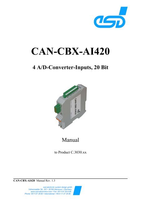
<strong>CAN</strong>-<strong>CBX</strong>-<strong>AI420</strong> Manual Rev. 1.3<br />
Manual<br />
to Product C.3030.xx<br />
<strong>esd</strong> electronic system design gmbh<br />
Vahrenwalder Str. 207 • 30165 Hannover • Germany<br />
www.<strong>esd</strong>-<strong>electronics</strong>.com • Fax: 0511/37 29 8-68<br />
Phone: 0511/37 29 80 • International: +49-5 11-37 29 80
N O T E<br />
The information in this document has been carefully checked and is believed to be entirely reliable. <strong>esd</strong><br />
makes no warranty of any kind with regard to the material in this document, and assumes no<br />
responsibility for any errors that may appear in this document. <strong>esd</strong> reserves the right to make changes<br />
without notice to this, or any of its products, to improve reliability, performance or design.<br />
<strong>esd</strong> assumes no responsibility for the use of any circuitry other than circuitry which is part of a product<br />
of <strong>esd</strong> gmbh.<br />
<strong>esd</strong> does not convey to the purchaser of the product described herein any license under the patent rights<br />
of <strong>esd</strong> gmbh nor the rights of others.<br />
<strong>esd</strong> electronic system design gmbh<br />
Vahrenwalder Str. 207<br />
30165 Hannover<br />
Germany<br />
Phone: +49-511-372 98-0<br />
Fax: +49-511-372 98-68<br />
E-mail: info@<strong>esd</strong>-<strong>electronics</strong>.com<br />
Internet: www.<strong>esd</strong>-<strong>electronics</strong>.com<br />
USA / Canada:<br />
<strong>esd</strong> <strong>electronics</strong> <strong>Inc</strong>.<br />
525 Bernardston Road<br />
Suite 1<br />
Greenfield, MA 01301<br />
USA<br />
Phone: +1-800-732-8006<br />
Fax: +1-800-732-8093<br />
E-mail: us-sales@<strong>esd</strong>-<strong>electronics</strong>.com<br />
Internet: www.<strong>esd</strong>-<strong>electronics</strong>.us<br />
<strong>CAN</strong>-<strong>CBX</strong>-<strong>AI420</strong> Manual Rev. 1.3
Document-File: I:\texte\Doku\MANUALS\<strong>CAN</strong>\<strong>CBX</strong>\<strong>AI420</strong>\Englisch\<strong>CAN</strong>-<strong>CBX</strong>-<strong>AI420</strong>_13.en9<br />
Date of print: 10.07.2006<br />
PCB version: from <strong>CAN</strong>-<strong>CBX</strong>-<strong>AI420</strong> Rev. 1.0<br />
Firmware version: from Rev. 1.8<br />
Changes in the chapters<br />
The changes in the document listed below affect changes in the hardware and firmware as well as<br />
changes in the description of facts only.<br />
Chapter Changes versus previous version<br />
- First English version<br />
Technical details are subject to change without further notice.<br />
<strong>CAN</strong>-<strong>CBX</strong>-<strong>AI420</strong> Manual Rev. 1.3
This page is intentionally left blank.<br />
<strong>CAN</strong>-<strong>CBX</strong>-<strong>AI420</strong> Manual Rev. 1.3
Contents<br />
1. Overview .................................................................3<br />
1.1 Description of the Module ..............................................3<br />
2. Technical Data .............................................................4<br />
2.1 General technical Data .................................................4<br />
2.2 CPU-Unit...........................................................4<br />
2.3 <strong>CAN</strong> Interface .......................................................5<br />
2.4 Analogue Inputs......................................................6<br />
2.5 Software-Support .....................................................6<br />
2.6 Order Information ....................................................7<br />
3. Hardware Installation .......................................................8<br />
3.1 Connecting Diagram...................................................8<br />
3.2 LED Display ........................................................9<br />
3.2.1 Indicator States ...............................................9<br />
3.2.2 Operation of the <strong>CAN</strong>-Error LED ................................ 10<br />
3.2.3 Operation of the <strong>CAN</strong>open-Status LED............................ 10<br />
3.2.4 Operation of the Error-LED .................................... 11<br />
3.2.5 Operation of the Power-LED.................................... 11<br />
3.2.6 Special Indicator States ........................................ 11<br />
3.3 Coding Switch ...................................................... 12<br />
3.3.1 Setting the Node-ID via Coding Switch ............................ 12<br />
3.3.2 Setting the Baud Rate ......................................... 13<br />
3.4 Installation of the Module Using Optional In-Rail Bus Connector................ 14<br />
3.4.1 Connecting Power Supply and <strong>CAN</strong>-Signals to <strong>CBX</strong>-In-Rail-Bus ........ 16<br />
3.5 Remove the <strong>CAN</strong>-<strong>CBX</strong> Module from the Optional In-Rail Bus ................. 17<br />
4. Description of the Units ..................................................... 18<br />
4.1 <strong>CAN</strong> Interface ...................................................... 18<br />
4.2 Analogue Inputs..................................................... 19<br />
5. Connector Assignment ..................................................... 20<br />
5.1 Power Supply Voltage X100 ........................................... 20<br />
5.2 <strong>CAN</strong>-Bus X400 ..................................................... 21<br />
5.3 <strong>CAN</strong> and Power Supply Voltage via In-Rail Bus Connector X101 ............... 22<br />
5.4 Analogue Inputs X500 ................................................ 23<br />
6. Correctly Wiring Electrically Isolated <strong>CAN</strong> Networks ............................ 24<br />
7. <strong>CAN</strong>-Bus Troubleshooting Guide ............................................. 28<br />
7.1 Termination ........................................................ 28<br />
7.2 <strong>CAN</strong>_H/<strong>CAN</strong>_L Voltage ............................................. 29<br />
7.3 Ground ........................................................... 29<br />
7.4 <strong>CAN</strong> Transceiver Resistance Test ....................................... 30<br />
8. Software ................................................................ 31<br />
8.1 Definition of Terms .................................................. 31<br />
8.2 NMT-Boot-up ...................................................... 32<br />
<strong>CAN</strong>-<strong>CBX</strong>-<strong>AI420</strong> Manual Rev. 1.3 1
2<br />
8.3 The <strong>CAN</strong>open-Object Directory......................................... 32<br />
8.3.1 Access on the Object Directory via SDOs .......................... 32<br />
8.4 Overview of used <strong>CAN</strong>open-Identifiers ................................... 36<br />
8.4.1 Setting the COB-ID........................................... 36<br />
8.5 Default PDO-Assignment .............................................. 37<br />
8.6 Reading the Analogue Values........................................... 38<br />
8.6.1 Messages of the Analogue Inputs................................. 38<br />
8.6.2 Supported Transmission Types Based on DS-301 .................... 38<br />
8.7 Implemented <strong>CAN</strong>open-Objects......................................... 39<br />
8.7.1 Device Type (1000 h) .......................................... 41<br />
8.7.2 Error Register (1001 h) ......................................... 42<br />
8.7.3 Pre-defined Error Field (1003 h) .................................. 43<br />
8.7.4 COB-ID of SYNC-Message (1005 h) .............................. 45<br />
8.7.5 Manufacturer’s Device Name (1008 h) ............................. 46<br />
8.7.6 Manufacturer’s Hardware Version (1009 h).......................... 47<br />
8.7.7 Manufacturer’s Software Version 100A h ........................... 47<br />
8.7.8 Guard Time (100C h) and Life Time Factor (100D h) ................... 48<br />
8.7.9 Node Guarding Identifier (100E h) ................................ 49<br />
8.7.10 Store Parameters (1010 h)...................................... 50<br />
8.7.11 Restore Default Parameters (1011 h) .............................. 51<br />
8.7.12 COB_ID Emergency Message (1014 h)............................ 52<br />
8.7.13 Inhibit Time EMCY (1015 h).................................... 53<br />
8.7.14 Consumer Heartbeat Time (1016 h)............................... 54<br />
8.7.15 Producer Heartbeat Time (1017 h) ............................... 56<br />
8.7.16 Identity Object (1018 h) ....................................... 57<br />
8.7.17 Verify Configuration (1020 h) ................................... 59<br />
8.7.18 Error Behaviour Object (1029 h) ................................. 60<br />
8.7.19 Object Transmit PDO Communication Parameter 1801 h, 1802 h ......... 61<br />
8.7.20 Transmit PDO Mapping Parameter 1A01 h, 1A02 h ................... 62<br />
8.8 Device Profile Area .................................................. 63<br />
8.8.1 Overview of the Implemented Objects 6401 h ...6426 h .................. 63<br />
8.8.2 Relationship Between the Implemented Objects for the Analogue Inputs . . . 63<br />
8.8.3 Read Input 16-Bit (6401 h) ...................................... 64<br />
8.8.4 Read Input 32-Bit (6402 h) ...................................... 66<br />
8.8.5 Analogue Input Interrupt Trigger (6421 h) .......................... 67<br />
8.8.6 Global Interrupt Enable (6423 h) .................................. 68<br />
8.8.7 Analogue Input Interrupt Delta (6426 h) ............................ 69<br />
8.9 Manufacturer Specific Profile Area....................................... 70<br />
8.9.1 Overview of the Manufacturer Specifc Objects 2310 h ... 2405 h ........... 70<br />
8.9.2 Sample Rate Set Point (2310 h)................................... 71<br />
8.9.3 Chopping Mode (2311 h) ....................................... 73<br />
8.9.4 Sample Rate Actual Value (2312 h)................................ 74<br />
8.9.5 Channel Enabled (2401 h) ....................................... 75<br />
8.9.6 Accu N (2402 h) .............................................. 76<br />
8.9.7 Average N (2403 h)............................................ 77<br />
8.9.8 Calibration Offset Value (2404 h) ................................. 78<br />
8.9.9 Calibration Gain Value (2405 h) .................................. 79<br />
8.10 Firmware-Update via DS-302-Objects (1F50 h...1F52 h) ....................... 80<br />
8.10.1 Download Control via Object 1F51 h .............................. 81<br />
<strong>CAN</strong>-<strong>CBX</strong>-<strong>AI420</strong> Manual Rev. 1.3
1. Overview<br />
1.1 Description of the Module<br />
C<br />
A<br />
N<br />
B<br />
U<br />
S<br />
<strong>CAN</strong> Connector<br />
MC1,5/5-GF-3,81<br />
ME-MAX<br />
Bus Connector<br />
Power Connector<br />
MSTBO 2,5/4-<br />
G1L-KMGY<br />
Electrical Isolation<br />
Physical<br />
<strong>CAN</strong><br />
Layer<br />
Power Supply<br />
24 V(DC)<br />
Digital<br />
Isolator<br />
+5 V=<br />
DC/DC<br />
Converter<br />
LEDs<br />
+5 V=<br />
<strong>CAN</strong><br />
Microcontroller<br />
MB90497<br />
DC/DC-<br />
Converter<br />
Overview<br />
Coding Switches<br />
<strong>CAN</strong> Baud Rate<br />
<strong>CAN</strong>open Node-ID<br />
<strong>CAN</strong>-<strong>CBX</strong>-<strong>AI420</strong> Manual Rev. 1.3 3<br />
Digital<br />
Isolator<br />
IL716-3<br />
Digital<br />
Isolator<br />
IL716-3<br />
4 Analog Inputs<br />
2-Channel<br />
24-bit -ADC<br />
AD7732BRU<br />
2-Channel<br />
24-bit -ADC<br />
AD7732BRU<br />
Fig. 1: Block circuit diagram of the <strong>CAN</strong>-<strong>CBX</strong>-<strong>AI420</strong> module<br />
Electrical Isolation<br />
I/O-Connector<br />
MC1,5/12-G-3,81-AU<br />
The <strong>CAN</strong>-<strong>CBX</strong>-<strong>AI420</strong> module is equipped with a MB90F497 microcontroller, which buffers the <strong>CAN</strong><br />
data into a local SRAM. The firmware is stored in the flash. Parameters are stored in a serial EEPROM.<br />
The four differential analogue inputs are converted by two sigma-delta-converters. The -converters<br />
offer a resolution of up to 24 bit. The resolution achieved during the operation depends essentially on<br />
the sample rate chosen and on the external circuit.<br />
The input voltage range of the analogue inputs is ±10 V.<br />
The inputs are connected via a 12-pin screw-/plug connector. The analogue inputs are electrically<br />
isolated by digital isolators for the protection of the other components.<br />
The power supply voltage and the <strong>CAN</strong>-bus connection can either be fed via the In-Rail bus connector,<br />
integrated in the top-hat rail or via separate plugs.<br />
The ISO 11898-compliant <strong>CAN</strong> interface allows a maximum data transfer rate of 1 Mbit/s. The <strong>CAN</strong><br />
interface is electrically isolated by a dual digital isolator and a DC/DC-converter.<br />
The <strong>CAN</strong>open node number and the <strong>CAN</strong> bit rate can be configured via three coding switches.
Technical Data<br />
2. Technical Data<br />
2.1 General technical Data<br />
4<br />
Power supply voltage<br />
Connectors<br />
nominal voltage: 24 V/DC<br />
input voltage range: 24 V ±20%<br />
current consumption (24 V, 20 C): approx. 56 mA<br />
X100 (4-pin COMBICON connector with spring-cage connection) -<br />
24 V-power supply voltage<br />
X101 (5-pin ME-MAX-TBUS-connector, Phoenix Contact) -<br />
<strong>CAN</strong> interface and power supply voltage via In-Rail bus<br />
X500 (12-pin Mini-COMBICON connector) - analogue inputs<br />
X400 (5-pin Mini-COMBICON connector) - <strong>CAN</strong> interface<br />
Only for test and programming purposes:<br />
X200 (6-pin COMBICON connector) -<br />
the connector is placed inside the case<br />
Temperature range -20 C ... +70 C ambient temperature<br />
Humidity max. 90%, non-condensing<br />
Dimensions<br />
Weight approx. 125 g<br />
2.2 CPU-Unit<br />
CPU 16 bit C MB90F497<br />
RAM 2 Kbyte integrated<br />
Flash 64 Kbyte integrated<br />
EEPROM min. 256 byte<br />
width: 2.2 cm, height: 11.2 cm, depth: 11.3 cm<br />
(including mounting rail fitting and connector projection)<br />
Table 1: General technical data of the module<br />
Table 2: Microcontroller<br />
<strong>CAN</strong>-<strong>CBX</strong>-<strong>AI420</strong> Manual Rev. 1.3
2.3 <strong>CAN</strong> Interface<br />
Number 1<br />
Connection<br />
<strong>CAN</strong> Controller<br />
Electrical isolation of <strong>CAN</strong><br />
interfaces against other units<br />
Physical layer <strong>CAN</strong><br />
Bustermination has to be set externally<br />
Technical Data<br />
5-pin COMBICON with spring-cage connection<br />
or via Phoenix Contact TBUS-connector (In-Rail-Bus)<br />
MB90F497, <strong>CAN</strong> 2.0A/B,<br />
(<strong>CAN</strong>open software supports only 11-bit <strong>CAN</strong> identifier)<br />
via dual digital isolator (ADUM120BR) and DC/DCconverters<br />
physical layer according to ISO 11898, transfer rate<br />
programmable from 10 Kbit/s up to 1 Mbit/s<br />
Table 3: Data of the <strong>CAN</strong> interface<br />
<strong>CAN</strong>-<strong>CBX</strong>-<strong>AI420</strong> Manual Rev. 1.3 5
Technical Data<br />
2.4 Analogue Inputs<br />
6<br />
Number 4 differential -converter inputs<br />
Converter-Type AD7732BRU<br />
Resolution resolution of the converter up to 24 bit<br />
Input voltage rage ±10 V<br />
Conversion time programmable<br />
Electrical isolation against other<br />
units<br />
Protective circuit<br />
2.5 Software-Support<br />
via magnetic data coupler<br />
Resistance against overvoltage of the converter inputs:<br />
- up to ±16,5 V without influence on the adjacent channel<br />
- absolute maximum ±50 V<br />
Table 4: Data of the analogue inputs<br />
The firmware of the module supports the <strong>CAN</strong>open standards DS-301 and DS-401.<br />
<strong>CAN</strong>-<strong>CBX</strong>-<strong>AI420</strong> Manual Rev. 1.3
2.6 Order Information<br />
<strong>CAN</strong>-<strong>CBX</strong>-<strong>AI420</strong><br />
Manuals<br />
Technical Data<br />
Type Features Order-No.<br />
<strong>CAN</strong>-<strong>CBX</strong>-<strong>AI420</strong>-ME Manual in English 1*)<br />
<strong>CAN</strong>-<strong>CBX</strong>-<strong>AI420</strong>-ENG<br />
Accessories<br />
<strong>CAN</strong>-<strong>CBX</strong>-TBUS<br />
<strong>CAN</strong>-<strong>CBX</strong>-TBUS-<br />
Connector<br />
<strong>CAN</strong>-<strong>CBX</strong>-<strong>AI420</strong><br />
4 analogue inputs, 20 bit,<br />
including 1x <strong>CAN</strong>-<strong>CBX</strong>-TBUS (C.3000.01)<br />
Engineering Manual in English 2*)<br />
Content: Circuit diagrams, PCB top overlay<br />
drawing, data sheets of significant components<br />
Mounting-rail bus connector of the <strong>CBX</strong>-In-<br />
Rail bus for <strong>CAN</strong>-<strong>CBX</strong>-modules,<br />
(a bus connector is included in delivery of the<br />
<strong>CAN</strong>-<strong>CBX</strong> module)<br />
Terminal plug of the <strong>CBX</strong>-In-Rail bus for the<br />
connection of the +24 V power supply voltage<br />
and the <strong>CAN</strong> interface<br />
1*) If module and manual are ordered together, the manual is free of charge.<br />
2*) This manual is liable for costs, please contact our support.<br />
Table 5: Order information<br />
C.3030.02<br />
C.3030.20<br />
C.3030.25<br />
C.3000.01<br />
C.3000.02<br />
<strong>CAN</strong>-<strong>CBX</strong>-<strong>AI420</strong> Manual Rev. 1.3 7
Hardware-Installation<br />
3. Hardware Installation<br />
3.1 Connecting Diagram<br />
8<br />
Fig. 2: Connections of the <strong>CAN</strong>-<strong>CBX</strong>-<strong>AI420</strong> module<br />
The connector pin assignment can be found on page 20 and the following.<br />
<strong>CAN</strong>-<strong>CBX</strong>-<strong>AI420</strong> Manual Rev. 1.3
3.2 LED Display<br />
Fig. 3: Position of the LEDs in the front panel<br />
Hardware-Installation<br />
The <strong>CAN</strong>-<strong>CBX</strong>-<strong>AI420</strong> module is equipped with four status LEDs. The terms of the indicator states of<br />
the LEDs are chosen in accordance with the <strong>CAN</strong>open Standard DS303-3, V 1.2 (chapter 3.1). The<br />
indicator states of the LEDs are described in the following chapters.<br />
3.2.1 Indicator States<br />
In principle there are 8 indicator states distinguished:<br />
Indicator state Display<br />
on LED constantly on<br />
off LED constantly off<br />
blinking LED blinking with a frequency of approx. 2.5 Hz<br />
flickering LED flickering with a frequency of approx. 10 Hz<br />
1 flash LED 200 ms on, 1400 ms off<br />
2 flashes LED 200 ms on, 200 ms off, 200 ms on 1000 ms off<br />
3 flashes LED 2x (200 ms on, 200 ms off) + 1x (200 ms on, 1000 ms off)<br />
4 flashes LED 3x (200 ms on, 200 ms off) + 1x (200 ms on, 1000 ms off)<br />
Table 6: Indicator states<br />
The red LED flashes opposite in phase with the green LED!<br />
<strong>CAN</strong>-<strong>CBX</strong>-<strong>AI420</strong> Manual Rev. 1.3 9
Hardware-Installation<br />
3.2.2 Operation of the <strong>CAN</strong>-Error LED<br />
10<br />
Label Name Colour<br />
LED indication Display function<br />
Component<br />
No.<br />
E <strong>CAN</strong> Error red 200A<br />
Indicator<br />
state<br />
off no error<br />
Description<br />
1 flash <strong>CAN</strong> controller is in Error Active state<br />
on <strong>CAN</strong> controller state is Bus Off<br />
2 flashes<br />
Table 7: Indicator states of the red <strong>CAN</strong> Error-LED<br />
3.2.3 Operation of the <strong>CAN</strong>open-Status LED<br />
Label Name Colour<br />
S<br />
<strong>CAN</strong>open<br />
Status<br />
Heartbeat or Nodeguard error occurred.<br />
The LED automatically turns off, if<br />
Nodeguard/Heartbeat-messages are received again.<br />
LED indication Display function<br />
Component<br />
No.<br />
green 200B<br />
Indicator<br />
state<br />
blinking Pre-operational<br />
on Operational<br />
1 flash Stopped<br />
Description<br />
3 flashes Module is in bootloader mode<br />
Table 8: Indicator states of the <strong>CAN</strong>open Status-LED<br />
<strong>CAN</strong>-<strong>CBX</strong>-<strong>AI420</strong> Manual Rev. 1.3
3.2.4 Operation of the Error-LED<br />
Hardware-Installation<br />
LED indication Display function<br />
Label Name Colour Component<br />
No.<br />
Indicator state Description<br />
M Error red 200C<br />
3.2.5 Operation of the Power-LED<br />
off no error<br />
on<br />
2 flashes<br />
blinking<br />
<strong>CAN</strong> Overrun Error<br />
The sample rate is set so high, that the firmware is not<br />
able to transmit all data on the <strong>CAN</strong> bus.<br />
Internal software error<br />
e.g.:<br />
- stored data have an invalid checksum therefore default<br />
values are loaded<br />
- internal watchdog has triggered<br />
- indicator state is continued until the module resets or<br />
an error occurs at the outputs.<br />
error of the A/D-input voltage<br />
input voltage of at least one channel 10V<br />
Table 9: Indicator state of the Error-LED<br />
LED indication Display function<br />
Label Name Colour Component<br />
No.<br />
Indicator state Description<br />
P Power green 200D<br />
3.2.6 Special Indicator States<br />
off no power supply voltage<br />
on power supply voltage is on<br />
Table 10: Indicator state of the Power-LED<br />
The indicator states described in the following table are indicated by the four status LEDs together:<br />
- red <strong>CAN</strong>-error LED is on<br />
- all other LEDs are off<br />
LED indication Description<br />
Table 11: Special indicator states<br />
Invalid Node-ID:<br />
The coding switches for the Node-ID are set to an<br />
invalid ID-value, the module is stopped<br />
<strong>CAN</strong>-<strong>CBX</strong>-<strong>AI420</strong> Manual Rev. 1.3 11
Hardware-Installation<br />
3.3 Coding Switch<br />
12<br />
<br />
Abb. 4: Position of the coding switches<br />
Attention!<br />
At the moment the module is switched ‘on’, the state of the coding switches is<br />
determined. Changes of the settings therefore have to be made before switching on the<br />
module, because changes of the settings are not determined during operation.<br />
After a reset (e.g. NMT reset) the settings are read again.<br />
3.3.1 Setting the Node-ID via Coding Switch<br />
The address range of the <strong>CAN</strong>-<strong>CBX</strong>-module can be set decimal from 1 to 127 or hexadecimal from 01 h<br />
to 7F h.<br />
The four higher-order bits (higher-order nibble) can be set with coding switch HIGH, the four lowerorder<br />
bits can be set with coding switch LOW.<br />
<strong>CAN</strong>-<strong>CBX</strong>-<strong>AI420</strong> Manual Rev. 1.3
3.3.2 Setting the Baud Rate<br />
The baud rate can be set with the coding switch Baud.<br />
Hardware-Installation<br />
Values from 0 h to F h can be set via the coding switch. The values of the baud rate can be taken from the<br />
following table:<br />
Setting<br />
[Hex]<br />
Bit rate<br />
[Kbit/s]<br />
0 1000<br />
1 666.6<br />
2 500<br />
3 333.3<br />
4 250<br />
5 166<br />
6 125<br />
7 100<br />
8 66.6<br />
9 50<br />
A 33.3<br />
B 20<br />
C 12.5<br />
D 10<br />
E reserved<br />
F reserved<br />
Table 12: Index of the baud rate<br />
<strong>CAN</strong>-<strong>CBX</strong>-<strong>AI420</strong> Manual Rev. 1.3 13
Hardware-Installation<br />
3.4 Installation of the Module Using Optional In-Rail Bus Connector<br />
If the <strong>CAN</strong> bus signals and the power supply voltage shall be fed via the In-Rail bus, please proceed<br />
as follows:<br />
14<br />
Figure 5: Mounting rail with bus connector<br />
1. Position the In-Rail bus connector on the mounting rail and snap it onto the mounting rail using<br />
slight pressure. Plug the bus connectors together to contact the communication and power<br />
signals (in parallel with one). The bus connectors can be plugged together before or after<br />
mounting the <strong>CAN</strong>-<strong>CBX</strong> modules.<br />
2. Place the <strong>CAN</strong>-<strong>CBX</strong> module with the DIN rail guideway on the top edge of the mounting rail.<br />
Figure 6 : Mounting <strong>CAN</strong>-<strong>CBX</strong> modules<br />
<strong>CAN</strong>-<strong>CBX</strong>-<strong>AI420</strong> Manual Rev. 1.3
Hardware-Installation<br />
3. Swivel the <strong>CAN</strong>-<strong>CBX</strong> module onto the mounting rail in pressing the module downwards<br />
according to the arrow as shown in figure 6. The housing is mechanically guided by the DIN rail<br />
bus connector.<br />
4. When mounting the <strong>CAN</strong>-<strong>CBX</strong> module the metal foot catch snaps on the bottom edge of the<br />
mounting rail. Now the module is mounted on the mounting rail and connected to the In-Rail<br />
bus via the bus connector. Connect the bus connectors and the In-Rail bus if not already done.<br />
Figure 7: Mounted <strong>CAN</strong>-<strong>CBX</strong> module<br />
<strong>CAN</strong>-<strong>CBX</strong>-<strong>AI420</strong> Manual Rev. 1.3 15
Hardware-Installation<br />
3.4.1 Connecting Power Supply and <strong>CAN</strong>-Signals to <strong>CBX</strong>-In-Rail-Bus<br />
To connect the power supply and the <strong>CAN</strong>-signals via the In-Rail bus, a terminal plug (order<br />
no.:C.3000.02) is needed. The terminal plug is not included in delivery and must be ordered separately<br />
(see order information).<br />
16<br />
Fig. 8: Mounting rail with In-Rail bus and terminal plug<br />
Plug the terminal plug into the socket on the right of the mounting-rail bus connector of the In-Rail bus,<br />
as described in Fig. 8. Then connect the <strong>CAN</strong> interface and the power supply voltage via the terminal<br />
plug.<br />
Fig. 9: <strong>CAN</strong>-<strong>CBX</strong> station with terminal plug<br />
A bus termination must be connected to the <strong>CAN</strong> connector of the <strong>CAN</strong>-<strong>CBX</strong> module at the end of the<br />
<strong>CBX</strong> station (see Fig. 9), if the <strong>CAN</strong> bus ends there.<br />
<strong>CAN</strong>-<strong>CBX</strong>-<strong>AI420</strong> Manual Rev. 1.3
Hardware-Installation<br />
Generally the <strong>CAN</strong> signals can be fed via the <strong>CAN</strong> connector of the first <strong>CAN</strong>-<strong>CBX</strong> module of the<br />
<strong>CBX</strong> station. The signals are then connected through the <strong>CAN</strong>-<strong>CBX</strong> station via the In-Rail bus. To lead<br />
through the <strong>CAN</strong>-signals the <strong>CAN</strong> bus connector of the last <strong>CAN</strong>-<strong>CBX</strong> module of the <strong>CAN</strong>-<strong>CBX</strong><br />
station (see Fig. 10) has to be used. The <strong>CAN</strong> connectors of the <strong>CAN</strong>-<strong>CBX</strong> modules which are not at<br />
the ends of the <strong>CAN</strong>-<strong>CBX</strong> station must not be connected to the <strong>CAN</strong> bus, because this would lead to<br />
incorrect branching.<br />
<br />
i<br />
Fig. 10: Connecting the <strong>CAN</strong> signals through the <strong>CAN</strong>-<strong>CBX</strong> station<br />
Attention!<br />
A feed through of the power supply voltage is not permissible! A feed through of<br />
the +24 V power supply voltage can cause damage on the <strong>CBX</strong> modules.<br />
3.5 Remove the <strong>CAN</strong>-<strong>CBX</strong> Module from the Optional In-Rail Bus<br />
If the <strong>CAN</strong>-<strong>CBX</strong> module is connected to the In-Rail bus please proceed as follows:<br />
Release the module from the mounting rail in moving the foot catch (see figure 7) downwards (e.g. with<br />
a screwdriver). Now the module is detached from the bottom edge of the mounting rail and can be<br />
removed.<br />
Note:<br />
It is possible to remove entire individual devices from the whole without interrupting<br />
the In-Rail bus connection, because the contact chain will not be interrupted.<br />
<strong>CAN</strong>-<strong>CBX</strong>-<strong>AI420</strong> Manual Rev. 1.3 17
18<br />
Descriptions of the Units<br />
4. Description of the Units<br />
4.1 <strong>CAN</strong> Interface<br />
An 82C251 is used as driver unit. The differential <strong>CAN</strong> bus signals are electrically isolated from the<br />
other signals via a dual digital converter (ADUM120BR) and a DC/DC-converter.<br />
<strong>CAN</strong>_Tx<br />
<strong>CAN</strong>_Rx<br />
VCC<br />
Dual Digital<br />
Isolator<br />
ADUM1201BR<br />
DC/DC<br />
RSS-0505<br />
VCC<br />
+ +<br />
VC05D150<br />
5V<br />
10µF<br />
GND<br />
-<br />
5V<br />
-<br />
<strong>CAN</strong>_GND<br />
2.2M<br />
2.2nF/250V~<br />
I1<br />
O1<br />
TX<br />
O2<br />
I2<br />
RX<br />
VCC1 VCC2<br />
VDD<br />
GND1 GND2<br />
R/GND<br />
2x 100nF<br />
<strong>CAN</strong> Transceiver<br />
PCA82C251<br />
BUSL<br />
BUSH<br />
GND<br />
+5V<br />
Fig. 11: <strong>CAN</strong> Interface<br />
X101<br />
Bus Connector MEMAX<br />
Shield<br />
(FE)<br />
VBB<br />
VBB_GND<br />
<strong>CAN</strong>_GND<br />
<strong>CAN</strong>_H<br />
<strong>CAN</strong>_L<br />
FE<br />
<strong>CAN</strong>_L<br />
<strong>CAN</strong>_H<br />
<strong>CAN</strong>_GND<br />
Shield<br />
<strong>CAN</strong>-<strong>CBX</strong>-<strong>AI420</strong> Manual Rev. 1.3<br />
4<br />
5<br />
3<br />
1<br />
2<br />
X400<br />
COMBICON<br />
MC 1,5/5-GF-3,81<br />
S (Connection<br />
to top hat rail)<br />
2<br />
4<br />
1<br />
3
4.2 Analogue Inputs<br />
to/from<br />
microcontroller<br />
<br />
Digital Isolator<br />
IL716<br />
Sigma-Delta A/D-Converter<br />
AD7732BRU<br />
DOUT<br />
DIN<br />
SCLK<br />
RDY#<br />
Electrical Isolation<br />
AIN0+<br />
AIN0-<br />
Description of the Units<br />
<strong>CAN</strong>-<strong>CBX</strong>-<strong>AI420</strong> Manual Rev. 1.3 19<br />
100p<br />
FE (Functional<br />
earth ground)<br />
100p<br />
FE (Functional<br />
earth ground)<br />
WE 74279207<br />
WE 74279207<br />
1P<br />
Pin 2<br />
1M<br />
Pin 3<br />
G<br />
Analog_GND<br />
Fig. 12: Analogue input circuit (example: channel 1)<br />
Principle of internal circuit of the<br />
Sigma-Delta A/D-converter<br />
AD7732BRU<br />
Converter<br />
Ref<br />
ca. 100k<br />
AIN+<br />
R SOURCE<br />
Pin 1<br />
X500<br />
Socket<br />
MC1,5/12-G-3,81-AU<br />
Attention: The internal circuit of the -converter (see figure below) and the wiring of<br />
the sensor signal cause a gain-error at the measuring. This fault is the smaller,<br />
the lower the resistance of the sensor is chosen.<br />
Furthermore the resistors of both measuring lines of the differential analogue<br />
inputs should be identical.<br />
Fig. 13: Principle of the internal circuit of the -converter<br />
The gain-error increases with increasing resistance R SOURCE (see figure above).
Steckerbelegung<br />
5. Connector Assignment<br />
5.1 Power Supply Voltage X100<br />
Device connector: COMBICON MSTBO 2,5/4-G1L-KMGY<br />
Line connector: COMBICON FKCT 2,5/4-ST, 5.0 mm pitch, spring-cage connection,<br />
PHOENIX-CONTACT order No.: 19 21 90 0 (included in the scope of<br />
delivery)<br />
20<br />
i<br />
Pin Position:<br />
Pin Assignment:<br />
Pin 4 3 2 1<br />
Signal<br />
P24<br />
(+ 24 V)<br />
M24<br />
(GND)<br />
Please refer also to the connecting diagram on page 8.<br />
Signal Description:<br />
M24<br />
(GND)<br />
P24<br />
(+ 24 V)<br />
Note: The pins 1 and 4 are connected to each other at the PCB.<br />
The pins 2 and 3 are connected to each other at the PCB.<br />
P24... power supply voltage +24 V<br />
M24... reference potential<br />
<strong>CAN</strong>-<strong>CBX</strong>-<strong>AI420</strong> Manual Rev. 1.3
5.2 <strong>CAN</strong>-Bus X400<br />
1<br />
2<br />
3<br />
4<br />
5<br />
Connector Assignment<br />
Device Connector: COMBICON MC 1,5/5-GF-3,81<br />
Line Connector: COMBICON FK-MCP 1,5/5-STF-3,81, spring-cage connection (included in the<br />
scope of delivery)<br />
Signal description:<br />
Pin Position: Pin-Assignment:<br />
(Illustration of device<br />
connector)<br />
Pin Signal<br />
1 <strong>CAN</strong>_GND<br />
2 <strong>CAN</strong>_L<br />
3 Shield<br />
4 <strong>CAN</strong>_H<br />
5 -<br />
<strong>CAN</strong>_L, <strong>CAN</strong>_H ... <strong>CAN</strong> signals<br />
<strong>CAN</strong>_GND ... reference potential of the local <strong>CAN</strong> physical layer<br />
Shield ... pin for line shield connection (using hat rail mounting direct contact to the<br />
mounting rail potential)<br />
- ... not connected<br />
Recommendation of an adapter cable from 5-pin Combicon (here line connector FK-MCP1,5/5-<br />
STF-3,81 with spring-cage-connection) to 9-pin DSUB:<br />
Figure 14: Assignment of the 9-pin DSUB-connector according to CiA DS 102.<br />
<strong>CAN</strong>-<strong>CBX</strong>-<strong>AI420</strong> Manual Rev. 1.3 21
Steckerbelegung<br />
5.3 <strong>CAN</strong> and Power Supply Voltage via In-Rail Bus Connector X101<br />
Connector type: Bus connector MEMAX<br />
ME 22,5 TBUS 1,5/5-ST-3,81 KMGY<br />
Signal Description:<br />
22<br />
Pin Position:<br />
Pin Assignment:<br />
Pin Signal<br />
5 M24 (GND)<br />
4 P24 (+24 V)<br />
3 <strong>CAN</strong>_GND<br />
2 <strong>CAN</strong>_L<br />
1 <strong>CAN</strong>_H<br />
S FE (PE_GND)<br />
<strong>CAN</strong>_L,<br />
<strong>CAN</strong>_H ... <strong>CAN</strong> signals<br />
<strong>CAN</strong>_GND ... reference potential of the local <strong>CAN</strong>-Physical layers<br />
P24... power supply voltage +24 V<br />
M24... reference potential<br />
FE... functional earth contact (EMC)(connected to mounting rail potential)<br />
<strong>CAN</strong>-<strong>CBX</strong>-<strong>AI420</strong> Manual Rev. 1.3
5.4 Analogue Inputs X500<br />
Device connector: COMBICON MC 1,5/12-GF-3,81<br />
Line connector: COMBICON MC 1,5/12-STF-3,81 (screw connection)<br />
(included in the scope of delivery)<br />
Signal description:<br />
Pin Assignment:<br />
Connector Assignment<br />
xP... positive input pin of the differential analogue input (x = 1, 2, 3, 4)<br />
xM... negative input pin of the differential analogue input(x = 1, 2, 3, 4)<br />
G ... reference potential analogue ground (connected to functional earth ground contact of<br />
the module)<br />
<strong>CAN</strong>-<strong>CBX</strong>-<strong>AI420</strong> Manual Rev. 1.3 23
24<br />
<strong>CAN</strong>_H<br />
<strong>CAN</strong>_L<br />
<strong>CAN</strong>_GND<br />
Wiring<br />
6. Correctly Wiring Electrically Isolated <strong>CAN</strong> Networks<br />
Generally all instructions applying for wiring regarding an electromagnetic compatible installation,<br />
wiring, cross sections of wires, material to be used, minimum distances, lightning protection, etc. have<br />
to be followed.<br />
The following general rules for the <strong>CAN</strong> wiring must be followed:<br />
1.<br />
2.<br />
3.<br />
A <strong>CAN</strong> net must not branch (exception: short dead-end feeders) and has to be terminated<br />
by the wave impedance of the wire (generally 120 W ±10%) at both ends (between the<br />
signals <strong>CAN</strong>_L and <strong>CAN</strong>_H and not at GND)!<br />
A <strong>CAN</strong> data wire requires two twisted wires and a wire to conduct the reference potential<br />
(<strong>CAN</strong>_GND)!<br />
For this the shield of the wire should be used!<br />
The reference potential <strong>CAN</strong>_GND has to be connected to the earth potential (PE) at one<br />
point. Exactly one connection to earth has to be established!<br />
4. The bit rate has to be adapted to the wire length.<br />
5. Dead-end feeders have to kept as short as possible (l < 0.3 m)!<br />
6.<br />
7.<br />
8.<br />
When using double shielded wires the external shield has to be connected to the earth<br />
potential (PE) at one point. There must be not more than one connection to earth.<br />
A suitable type of wire (wave impedance ca. 120 ±10%) has to be used and the voltage<br />
loss in the wire has to be considered!<br />
<strong>CAN</strong> wires should not be laid directly next to disturbing sources. If this cannot be avoided,<br />
double shielded wires are preferable.<br />
Wire structure Signal assignment of wire and connection of earthing and terminator<br />
Shielded wire with<br />
transposed wires<br />
120 Ohm<br />
<strong>CAN</strong> wire with connectors<br />
DSUB9 connector<br />
(female or male)<br />
<strong>CAN</strong>_GND<br />
DSUB9 connector<br />
(female or male)<br />
pin designation<br />
(at wire shield)<br />
pin designation<br />
1<br />
2<br />
n.c.<br />
<strong>CAN</strong>_L<br />
n.c. 1<br />
2<br />
3<br />
3<br />
4 n.c.<br />
n.c. 4<br />
5 n.c.<br />
n.c. 5<br />
6<br />
7<br />
n.c.<br />
<strong>CAN</strong>_H<br />
n.c. 6<br />
7<br />
8 n.c.<br />
n.c. 8<br />
9 n.c.<br />
n.c. 9<br />
connector case n.c.<br />
n.c. connector case<br />
n.c. = not connected<br />
Figure: Structure and connection of wire<br />
<strong>CAN</strong>-<strong>CBX</strong>-<strong>AI420</strong> Manual Rev. 1.3<br />
120 Ohm<br />
earth (PE)
Cabling<br />
l < 0,3 m<br />
<strong>CAN</strong>-CBM-<br />
DIO8<br />
<strong>CAN</strong>-CBM-<br />
AI4<br />
Wiring<br />
for devices which have only one <strong>CAN</strong> connector per net use T-connector and dead-end feeder<br />
(shorter than 0.3 m) (available as accessory)<br />
<strong>CAN</strong>-Board<br />
Net 1<br />
e.g. PCI/405,<br />
<strong>CAN</strong>-USB,<br />
VME-<strong>CAN</strong>2, etc.<br />
Net 2<br />
Connecting<br />
<strong>CAN</strong>_GND to<br />
Protective Conductor PE<br />
Terminator<br />
PE<br />
with PE Connector<br />
T-Connector<br />
Order-no.: C.1311.03<br />
Terminal Resistance<br />
T-Connector<br />
C.1311.03<br />
<strong>CAN</strong>-Cable<br />
Order-no.: C.1323.03<br />
l < 0,3 m<br />
T-Connector<br />
C.1311.03<br />
<strong>CAN</strong>-Cable<br />
Order-no.: C.1323.03<br />
<strong>CAN</strong>-<strong>CBX</strong>-<strong>AI420</strong> Manual Rev. 1.3 25<br />
<strong>CAN</strong>_H<br />
<strong>CAN</strong>_L<br />
<strong>CAN</strong>_GND<br />
l < 0,3 m<br />
<strong>CAN</strong>-CBM-<br />
COM1<br />
T-Connector<br />
C.1311.03<br />
Female Connector<br />
Male Connector<br />
Male Terminator<br />
(Order-no.: C.1302.01)<br />
Female Terminator<br />
(Order-no.: C.1301.01)<br />
l < 0,3 m<br />
<strong>CAN</strong>-Cable<br />
Order-no.: C.1323.03<br />
Figure: Example for correct wiring (when using single shielded wires)<br />
use external terminator, because this can later be found again more easily!<br />
T-Connector<br />
C.1311.03<br />
Terminator<br />
l < 0,3 m<br />
e.g.<br />
<strong>CAN</strong>-SPS Interface<br />
CSC595/2<br />
or<br />
<strong>CAN</strong>-PC Board<br />
9-pin DSUB-terminator with male and female contacts and earth terminal are available as<br />
accessories<br />
Earthing<br />
<strong>CAN</strong>_GND has to be conducted in the <strong>CAN</strong> wire, because the individual <strong>esd</strong> modules are<br />
electrically isolated from each other!<br />
<strong>CAN</strong>_GND has to be connected to the earth potential (PE) at exactly one point in the net!<br />
each <strong>CAN</strong> user without electrically isolated interface works as an earthing, therefore: do not<br />
connect more than one user without potential separation!<br />
Earthing <strong>CAN</strong> e.g. be made at a connector
Wiring<br />
Wire Length<br />
Optical couplers are delaying the <strong>CAN</strong> signals. By using fast optical couplers and testing each<br />
board at 1 Mbit/s, however, <strong>esd</strong> <strong>CAN</strong> guarantee a reachable length of 37 m at 1 Mbit/s for most<br />
<strong>esd</strong> <strong>CAN</strong> modules within a closed net without impedance disturbances like e.g. longer dead-end<br />
feeders. (Exception: <strong>CAN</strong>-CBM-DIO8, -AI4 and AO4 (these modules work only up to 10 m with<br />
1 Mbit/s))<br />
26<br />
Bit rate<br />
[Kbit/s]<br />
1000<br />
800<br />
666.6<br />
500<br />
333.3<br />
250<br />
166<br />
125<br />
100<br />
66.6<br />
50<br />
33.3<br />
20<br />
12.5<br />
10<br />
Typical values of reachable<br />
wire length with <strong>esd</strong><br />
interface l max [m]<br />
37<br />
59<br />
80<br />
130<br />
180<br />
270<br />
420<br />
570<br />
710<br />
1000<br />
1400<br />
2000<br />
3600<br />
5400<br />
7300<br />
CiA recommendations<br />
(07/95) for reachable wire<br />
lengths l min [m]<br />
25<br />
50<br />
-<br />
100<br />
-<br />
250<br />
-<br />
500<br />
650<br />
-<br />
1000<br />
-<br />
2500<br />
-<br />
5000<br />
Table: Reachable wire lengths depending on the bit rate when using <strong>esd</strong>-<strong>CAN</strong> interfaces<br />
<strong>CAN</strong>-<strong>CBX</strong>-<strong>AI420</strong> Manual Rev. 1.3
Examples for <strong>CAN</strong> Wires<br />
Manufacturer Type of wire<br />
U.I. LAPP GmbH<br />
Schulze-Delitzsch-Straße 25<br />
70565 Stuttgart<br />
Germany<br />
www.lappkabel.de<br />
ConCab GmbH<br />
Äußerer Eichwald<br />
74535 Mainhardt<br />
Germany<br />
www.concab.de<br />
SAB Bröckskes GmbH&Co. KG<br />
Grefrather Straße 204-212b<br />
41749 Viersen<br />
Germany<br />
www.sab-brockskes.de<br />
Wiring<br />
e.g.<br />
UNITRONIC ®-BUS <strong>CAN</strong> UL/CSA (UL/CSA approved)<br />
UNITRONIC ®-BUS-FD P <strong>CAN</strong> UL/CSA (UL/CSA approved)<br />
e.g.<br />
BUS-PVC-C (1 x 2 x 0.22 mm²) Order No.: 93 022 016 (UL appr.)<br />
BUS-Schleppflex-PUR-C (1 x 2 x 0.25 mm²) Order No.: 94 025 016 (UL appr.)<br />
e.g.<br />
SABIX ® CB 620 (1 x 2 x 0.25 mm²) Order No.: 56202251<br />
CB 627 (1 x 2 x 0.25 mm²) Order No.: 06272251 (UL appr.)<br />
Note: Completely configured <strong>CAN</strong> wires can be ordered from <strong>esd</strong>.<br />
<strong>CAN</strong>-<strong>CBX</strong>-<strong>AI420</strong> Manual Rev. 1.3 27
28<br />
<strong>CAN</strong>-Bus Troubleshooting Guide<br />
7. <strong>CAN</strong>-Bus Troubleshooting Guide<br />
The <strong>CAN</strong>-Bus Troubleshooting Guide is a guide to find and eliminate the most frequent hardware-error<br />
causes in the wiring of <strong>CAN</strong>-networks.<br />
120 <br />
<strong>CAN</strong>_H<br />
<strong>CAN</strong>_L<br />
<strong>CAN</strong>_GND<br />
Figure: Simplified diagram of a <strong>CAN</strong> network<br />
7.1 Termination<br />
<strong>CAN</strong>_H<br />
<strong>CAN</strong>_L<br />
<strong>CAN</strong>_GND<br />
2 3<br />
The termination is used to match impedance of a node to the impedance of the transmission line being<br />
used. When impedance is mismatched, the transmitted signal is not completely absorbed by the load<br />
and a portion is reflected back into the transmission line. If the source, transmission line and load<br />
impedance are equal these reflections are eliminated. This test measures the series resistance of the<br />
<strong>CAN</strong> data pair conductors and the attached terminating resistors.<br />
To test it, please<br />
1. Turn off all power supplies of the attached <strong>CAN</strong> nodes.<br />
2. Measure the DC resistance between <strong>CAN</strong>_H and <strong>CAN</strong>_L at the middle and ends of<br />
the network 1 (see figure above).<br />
The measured value should be between 50 and 70 . The measured value should be nearly the same<br />
at each point of the network.<br />
If the value is below 50 , please make sure that:<br />
- there is no short circuit between <strong>CAN</strong>_H and <strong>CAN</strong>_L wiring<br />
- there are not more than two terminating resistors<br />
- the nodes do not have faulty transceivers.<br />
If the value is higher than 70 , please make sure that:<br />
- there are no open circuits in <strong>CAN</strong>_H or <strong>CAN</strong>_L wiring<br />
- your bus system has two terminating resistors (one at each end) and that they are 120 each.<br />
V<br />
120 <br />
<strong>CAN</strong>-<strong>CBX</strong>-<strong>AI420</strong> Manual Rev. 1.3<br />
V<br />
<br />
1
7.2 <strong>CAN</strong>_H/<strong>CAN</strong>_L Voltage<br />
<strong>CAN</strong>-Bus Troubleshooting Guide<br />
Each node contains a <strong>CAN</strong> transceiver that outputs differential signals. When the network<br />
communication is idle the <strong>CAN</strong>_H and <strong>CAN</strong>_L voltages are approximately 2.5 volts. Faulty<br />
transceivers can cause the idle voltages to vary and disrupt network communication.<br />
To test for faulty transceivers, please<br />
1. Turn on all supplies.<br />
2. Stop all network communication.<br />
3. Measure the DC voltage between <strong>CAN</strong>_H and GND 2 (see figure above).<br />
4. Measure the DC voltage between <strong>CAN</strong>_L and GND 3 (see figure above).<br />
Normally the voltage should be between 2.0 V and 4.0 V.<br />
If it is lower than 2.0 V or higher than 4.0 V, it is possible that one or more nodes have faulty<br />
transceivers. For a voltage lower than 2.0 V please check <strong>CAN</strong>_H and <strong>CAN</strong>_L conductors for<br />
continuity. For a voltage higher than 4.0 V, please check for excessive voltage.<br />
To find the node with a faulty transceiver please test the <strong>CAN</strong> transceiver resistance (see next page).<br />
7.3 Ground<br />
The shield of the <strong>CAN</strong> network has to be grounded at only one location. This test will indicate if the<br />
shielding is grounded in several places.<br />
To test it, please<br />
1. Disconnect the shield wire from the ground.<br />
2. Measure the DC resistance between Shield and ground.<br />
3. Connect Shield wire to ground.<br />
The resistance should be higher than 1 M . If it is lower, please search for additional grounding of the<br />
shield wires.<br />
<strong>CAN</strong>-<strong>CBX</strong>-<strong>AI420</strong> Manual Rev. 1.3 29
30<br />
<strong>CAN</strong>-Bus Troubleshooting Guide<br />
7.4 <strong>CAN</strong> Transceiver Resistance Test<br />
<strong>CAN</strong> transceivers have one circuit that controls <strong>CAN</strong>_H and another circuit that controls <strong>CAN</strong>_L.<br />
Experience has shown that electrical damage to one or both of the circuits may increase the leakage<br />
current in these circuits.<br />
To measure the current leakage through the <strong>CAN</strong> circuits, please use an resistance measuring device<br />
and:<br />
1. Disconnect the node from the network. Leave the node unpowered 4 (see figure below).<br />
2. Measure the DC resistance between <strong>CAN</strong>_H and <strong>CAN</strong>_GND 5 (see figure below).<br />
3. Measure the DC resistance between <strong>CAN</strong>_L and <strong>CAN</strong>_GND 6 (see figure below).<br />
Normally the resistance should be between 1 M and 4 M or higher. If it is lower than this range,<br />
the <strong>CAN</strong> transceiver is probably faulty.<br />
<strong>CAN</strong>-node<br />
<strong>CAN</strong>-<br />
Transceiver<br />
<strong>CAN</strong>_H<br />
<strong>CAN</strong>_L<br />
<strong>CAN</strong>_GND<br />
Power<br />
4<br />
Disconnect<br />
Power !<br />
5 6<br />
<br />
<br />
Figure: Simplified diagram of a <strong>CAN</strong> node<br />
4<br />
Disconnect<br />
<strong>CAN</strong> !<br />
<strong>CAN</strong>-<strong>CBX</strong>-<strong>AI420</strong> Manual Rev. 1.3
8. Software<br />
<strong>CAN</strong>open-Software<br />
Apart from basic descriptions of the <strong>CAN</strong>open, this chapter contains the most significant information<br />
about the implemented functions.<br />
A complete <strong>CAN</strong>open description is too extensive for the purpose of this manual.<br />
Further information can therefore be taken from the CAL/<strong>CAN</strong>open documentation ‘CiA Draft<br />
Standard 301, V 4.02’ and ‘CiA Draft Standard Proposal 401, V 2.1’.<br />
8.1 Definition of Terms<br />
COB ... Communication Object<br />
Emergency-Id... Emergency Data Object<br />
NMT... Network Management (Master)<br />
Rx... receive<br />
SDO... Service Data Object<br />
Sync... Sync(frame) Telegram<br />
Tx... transmit<br />
PDOs (Process Data Objects)<br />
PDOs are used to transmit process data.<br />
In the ‘Transmit’-PDO (TxPDO) the <strong>CAN</strong>-<strong>CBX</strong>-<strong>AI420</strong> module transmits data to the <strong>CAN</strong>open<br />
network.<br />
SDOs (Service Data Objects)<br />
SDOs are used to transmit module internal configuration- and parameter data. In opposition to<br />
the PDOs SDO-messages are confirmed. A write or read request on a data object is always<br />
answered by a response telegram with an error index.<br />
<strong>CAN</strong>-<strong>CBX</strong>-<strong>AI420</strong> Manual Rev. 1.3 31
<strong>CAN</strong>open-Software<br />
8.2 NMT-Boot-up<br />
The <strong>CAN</strong>-<strong>CBX</strong>-<strong>AI420</strong> module can be initialized with the ‘Minimum Capability Device’ boot-up as<br />
described in CiA-Draft Standard 301 in chapter 9.4.<br />
Usually a telegram to switch from Pre-Operational status to Operational status after boot-up is<br />
sufficient. For this the 2-byte telegram ‘01 h’, ‘00 h’, for example, has to be transmitted to <strong>CAN</strong>-identifier<br />
‘0000 h’ (= Start Remote Node all Devices).<br />
8.3 The <strong>CAN</strong>open-Object Directory<br />
The object directory is basically a (sorted) group of objects which can be accessed via the <strong>CAN</strong><br />
network. Each object in this directory is addressed with a 16-bit index. The index in the object<br />
directories is represented in hexadecimal format.<br />
The index can be a 16-bit parameter in accordance with the <strong>CAN</strong>open specification (CiA-Draft DS 301)<br />
or a manufacturer-specific code. By means of the MSBs of the index the object class of the parameter<br />
is defined.<br />
Part of the object directory are among others:<br />
32<br />
Index<br />
[Hex]<br />
Object Example<br />
0001 ... 009F definition of data types -<br />
1000 ... 1FFF Communication Profile Area 1001 h : Error register<br />
2000 ... 5FFF Manufacturer Specific Profile Area 2310 h : Sample rate<br />
6000 ... 9FFF Standardized Device Profile Area according to Device Profile DS 40x<br />
A000 ... FFFF reserved -<br />
8.3.1 Access on the Object Directory via SDOs<br />
The SDOs (Service Data Objects) are used to get access to the object directory of a device.<br />
An SDO therefore represents a ‘channel’ to access the parameter of the device. The access via this<br />
channel can be made in <strong>CAN</strong>-<strong>CBX</strong>-<strong>AI420</strong> module state Operational and Pre-operational.<br />
The SDOs are transmitted on ID ‘600 h + NodeID’ (request). The receiver acknowledges the parameter<br />
on ID ‘580 h + NodeID’ (response).<br />
<strong>CAN</strong>-<strong>CBX</strong>-<strong>AI420</strong> Manual Rev. 1.3
An SDO is structured as follows:<br />
Identifier Command<br />
code<br />
Example:<br />
600 h+<br />
Node-ID<br />
Index<br />
(low) (high)<br />
<strong>CAN</strong>open-Software<br />
Sub-index LSB Data field MSB<br />
23 h 00 14 h 01 7F h 04 h 00 00<br />
(write)<br />
Description of the SDOs:<br />
(Index=1400 h)<br />
(Receive-PDO-Comm-Para)<br />
(COB-def.) COB = 047F h<br />
Identifier ....... The parameters are transmitted on ID ‘600 h + NodeID’ (request).<br />
The receiver acknowledges the parameters on ID ‘580 h + NodeID’ (response).<br />
Command code . . The command code transmitted consists among other things of the command<br />
specifier and the length. Frequently required combinations are, for instance:<br />
40 h = 64 dec : Read Request, i.e. a parameter is to be read<br />
23 h = 35 dec : Write Request with 32-bit data, i.e. a parameter is to be set<br />
The <strong>CAN</strong>-<strong>CBX</strong>-<strong>AI420</strong> module responds to every received telegram with a<br />
response telegram. This can contain the following command codes:<br />
43 h = 67 dec : Read Response with 32 bit data, this telegram contains the<br />
parameter requested<br />
60 h = 96 dec : Write Response, i.e. a parameter has been set successfully<br />
80 h = 128 dec : Error Response, i.e. the <strong>CAN</strong> module reports a communication error<br />
<strong>CAN</strong>-<strong>CBX</strong>-<strong>AI420</strong> Manual Rev. 1.3 33
34<br />
<strong>CAN</strong>open-Software<br />
Frequently Used Command Codes<br />
The following table summarizes frequently used command codes. The command<br />
frames must always contain 8 data bytes. Notes on the syntax and further command<br />
codes can be found in CiA DS 301, chapter “Service Data Object”.<br />
Command<br />
Write Request<br />
(Initiate Domain Download)<br />
Write Response<br />
(Initiate Domain Download)<br />
Read Request<br />
(Initiate Domain Upload)<br />
Read Response<br />
(Initiate Domain Upload)<br />
Error Response<br />
(Abort Domain Transfer)<br />
Number of data<br />
bytes<br />
1<br />
2<br />
3<br />
4<br />
Command code<br />
[Hex]<br />
2F<br />
2B<br />
27<br />
23<br />
- 60<br />
- 40<br />
1<br />
2<br />
3<br />
4<br />
4F<br />
4B<br />
47<br />
43<br />
- 80<br />
Index, Sub-Index . Index and sub-index will be described in the chapters “Device Profile Area” and<br />
“Manufacturer Specific Objects” of this manual.<br />
Data Field ...... The data field has got a size of a maximum of 4 bytes and is always structured<br />
‘LSB first, MSB last’. The least significant byte is always in ‘Data 1’. With 16-bit<br />
values the most significant byte (bits 8...15) is always in ‘Data 2’, and with 32-bit<br />
values the MSB (bits 24...31) is always in ‘Data 4’.<br />
<strong>CAN</strong>-<strong>CBX</strong>-<strong>AI420</strong> Manual Rev. 1.3
Error Codes of the SDO Domain Transfer<br />
<strong>CAN</strong>open-Software<br />
The following error codes might occur (according to CiA DS 301, chapter “Abort SDO Transfer<br />
Protocol”):<br />
Abort code<br />
[Hex]<br />
Description<br />
0x05040001 wrong command specifier<br />
0x06010002 wrong write access<br />
0x06020000 wrong index<br />
0x06040041 object can not be mapped to PDO<br />
0x06060000 access failed due to an hardware error<br />
0x06070010 wrong number of data bytes<br />
0x06070012 service parameter too long<br />
0x06070013 service parameter too small<br />
0x06090011 wrong sub-index<br />
0x06090030 transmitted parameter is outside the accepted value range<br />
0x08000000 undefined cause of error<br />
0x08000020 data cannot be transferred or stored in the application<br />
0x08000022<br />
data cannot be transferred or stored in the application because of the present<br />
device state<br />
0x08000024 access to flash failed<br />
<strong>CAN</strong>-<strong>CBX</strong>-<strong>AI420</strong> Manual Rev. 1.3 35
<strong>CAN</strong>open-Software<br />
8.4 Overview of used <strong>CAN</strong>open-Identifiers<br />
36<br />
Function<br />
Identifier<br />
[Hex]<br />
Network management 0 NMT<br />
Description<br />
SYNC 80 Sync to all, (configurable via object 1005 h)<br />
Emergency Message 80 + NodeID configurable via object 1014 h<br />
Tx-PDO2 280 + NodeID PDO2 from <strong>CAN</strong>-<strong>CBX</strong>-<strong>AI420</strong> (Tx) (object 1801 h)<br />
Tx-PDO3 380 + NodeID PDO3 from <strong>CAN</strong>-<strong>CBX</strong>-<strong>AI420</strong> (Tx) (object 1802 h)<br />
Tx-SDO 580 + Node-ID SDO from <strong>CAN</strong>-<strong>CBX</strong>-<strong>AI420</strong> (Tx)<br />
Rx-SDO 600 + Node-ID SDO from <strong>CAN</strong>-<strong>CBX</strong>-<strong>AI420</strong> (Rx)<br />
Node Guarding 700 + NodeID configurable via object 100E h<br />
NodeID: <strong>CAN</strong>open address [1 h...7F h]<br />
8.4.1 Setting the COB-ID<br />
The COB-IDs which can be set (except the one of SYNC), are deduced initially from the setting of the<br />
Node-ID via the coding switches (see page 12). If the COB-IDs are set via SDO, this setting is valid<br />
even if the coding switches are set to another Node-ID after that.<br />
To accept the Node-ID from the coding switches again, the Comm defaults or all defaults have to be<br />
restored (object 1011 h)<br />
<strong>CAN</strong>-<strong>CBX</strong>-<strong>AI420</strong> Manual Rev. 1.3
8.5 Default PDO-Assignment<br />
<strong>CAN</strong>open-Software<br />
PDOs (Process Data Objects) are used to transmit process data. The PDO mapping can be changed. The<br />
following tables show the default mapping at delivery of the module:<br />
PDO <strong>CAN</strong> identifier Length Transmission direction Default assignment<br />
TxPDO1 n.a. n.a. n.a. TxPDO1 is not used<br />
TxPDO2 280 h + Node-ID 8 byte<br />
TxPDO3 380 h + Node-ID 8 byte<br />
Tx-PDO2 (<strong>CAN</strong>-<strong>CBX</strong>-<strong>AI420</strong> ->)<br />
from <strong>CAN</strong>-<strong>CBX</strong>-<strong>AI420</strong><br />
(Tx/Transmit-PDO)<br />
from <strong>CAN</strong>-<strong>CBX</strong>-<strong>AI420</strong><br />
(Tx/Transmit-PDO)<br />
A/D-values channel 1 to 2<br />
as 32-bit values<br />
A/D-values channel 3 to 4<br />
as 32 bit values<br />
<strong>CAN</strong>-Identifier: 280h + Node-ID<br />
Byte 0 1 2 3 4 5 6 7<br />
Parameter Read_Analogue_Input_32-Bit_1 Read_Analogue_Input_32-Bit_2<br />
Tx-PDO3 (<strong>CAN</strong>-<strong>CBX</strong>-<strong>AI420</strong> ->)<br />
<strong>CAN</strong>-Identifier: 380h + Node-ID<br />
Byte 0 1 2 3 4 5 6 7<br />
Parameter Read_Analogue_Input_32-Bit_3 Read_Analogue_Input_32-Bit_4<br />
<strong>CAN</strong>-<strong>CBX</strong>-<strong>AI420</strong> Manual Rev. 1.3 37
38<br />
<strong>CAN</strong>open-Software<br />
8.6 Reading the Analogue Values<br />
8.6.1 Messages of the Analogue Inputs<br />
The transmission types for the analogue inputs are described in the following:<br />
acyclic, synchronous: The transmission is initiated if a SYNC-message has been received (PDOtransmission<br />
type 0) and data has changed.<br />
cyclic, synchronous: The transmission is initiated if a defined number of SYNC-messages has been<br />
received (PDO-transmission type 1...240).<br />
synchronous, remote request: The state of the inputs is latched with each SYNC-message and is<br />
transmitted after the reception of an RTR-frame (PDO-transmission type 252).<br />
asynchronous, remote request: After the reception of an RTR-frame the last determined state of the<br />
inputs is transmitted (PDO-transmission type 253).<br />
event controlled, asynchronous: The transmission is initiated if the state of selected inputs has<br />
changed (PDO-transmission type 254, 255).<br />
8.6.2 Supported Transmission Types Based on DS-301<br />
Transmission<br />
Type<br />
cyclic acyclic<br />
PDO-Transmission<br />
synchronous<br />
asynchronous<br />
RTR<br />
supported by<br />
<strong>CAN</strong>-<strong>CBX</strong>-<strong>AI420</strong><br />
0 X X x<br />
1...240 X X x<br />
241...251 reserved -<br />
252 X X x<br />
253 X X x<br />
254 X X x<br />
255 X X x<br />
<strong>CAN</strong>-<strong>CBX</strong>-<strong>AI420</strong> Manual Rev. 1.3
8.7 Implemented <strong>CAN</strong>open-Objects<br />
A detailed description of the objects can be taken from CiA DS-301.<br />
Index<br />
[Hex]<br />
Sub-index<br />
(max.) [Dec]<br />
Implemented <strong>CAN</strong>open Objects<br />
Description Data type R/W Default value<br />
1000 - Device Type unsigned 32 ro 00040191 h<br />
1001 - Error Register unsigned 8 ro 00 h<br />
1003 10 Pre-Defined-Error-Field unsigned32 rw 00 h<br />
1005 - COB-ID-Sync unsigned32 rw 80 h<br />
1008 - Manufacturer’s Device Name visible string ro “<strong>CAN</strong>-<strong>CBX</strong>-<strong>AI420</strong>”<br />
1009 - Manufacturer’s Hardware Version visible string ro<br />
100A - Manufacturer’s Software Version visible string ro<br />
100C - Guard Time unsigned 16 rw 0000 h<br />
100D - Life Time Factor unsigned 8 rw 00 h<br />
x.yy (depending on<br />
version)<br />
x.yy (depending on<br />
version)<br />
100E - Node Guarding Identifier unsigned 32 rw Node-ID + 700 h<br />
1010 3 Store Parameter unsigned 32 rw<br />
1011 3 Restore Parameter unsigned 32 rw<br />
1014 - COB-ID Emergency Object unsigned 32 rw 80 h + Node-ID<br />
1015 - Inhibit Time EMCY unsigned 16 rw 00 h<br />
1016 1 Consumer Heartbeat Time unsigned 32 rw 00 h<br />
1017 - Producer Heartbeat Time unsigned 16 rw 00 h<br />
1018 4 Identity Object unsigned 32 ro<br />
1029 3 Error Behaviour unsigned 8 ro 00 h<br />
Vendor Id: 00000017 h<br />
Prod. Code: 23030002 h<br />
<strong>CAN</strong>-<strong>CBX</strong>-<strong>AI420</strong> Manual Rev. 1.3 39
40<br />
Index<br />
[Hex]<br />
Implemented <strong>CAN</strong>open Objects<br />
Subindex<br />
(max.)<br />
[Dec]<br />
Description Data type R/W<br />
1801 5 2. Transmit PDO-Parameter PDO CommPar (20 h) rw<br />
1802 5 3. Transmit PDO-Parameter PDO CommPar (20 h) rw<br />
1A01 2 2. Transmit PDO-Mapping PDO Mappping (21 h) rw<br />
1A02 2 3. Transmit PDO-Mapping PDO Mappping (21 h) rw<br />
<strong>CAN</strong>-<strong>CBX</strong>-<strong>AI420</strong> Manual Rev. 1.3
8.7.1 Device Type (1000 h)<br />
INDEX 1000h Name device type<br />
Data Type unsigned 32<br />
Access Type ro<br />
Default Value 0004 0191<br />
The value of the device type is: 0004.0191 h<br />
Example: Reading des Device Type<br />
Implemented <strong>CAN</strong>open Objects<br />
(Analogue input: 0004 h<br />
digital profile number: 0191 h )<br />
The <strong>CAN</strong>open master transmits the read request on identifier ‘603 h’ (600 h + Node-ID) to the <strong>CAN</strong>-<br />
<strong>CBX</strong>-<strong>AI420</strong> module with the module no. 3 (Node-ID=3 h):<br />
ID RTR LEN DATA<br />
1 2 3 4 5 6 7 8<br />
603 h 0 h 8 h 40 h 00 h 10 h 00 h 00 h 00 h 00 h 00 h<br />
Read<br />
Request<br />
Index=1000 h<br />
The <strong>CAN</strong>-<strong>CBX</strong>-<strong>AI420</strong> module no. 3 responds to the master by means of read response on identifier<br />
‘583 h’ (580 h + Node-ID) with the value of the device type:<br />
<strong>CAN</strong>-<strong>CBX</strong>-<strong>AI420</strong> Manual Rev. 1.3 41<br />
Sub<br />
Index<br />
ID RTR LEN DATA<br />
1 2 3 4 5 6 7 8<br />
583 h 0 h 8 h 43 h 00 h 10 h 00 h 91 h 01 h 04 h 00 h<br />
Read<br />
Response<br />
value of device type: 0004.0191 h<br />
Index=1000 h Sub Index dig. Profile Nr.191 Analogue Input<br />
The data field is always structured following the rule ‘LSB first, MSB last‘ (see page 34, data field).
42<br />
Implemented <strong>CAN</strong>open Objects<br />
8.7.2 Error Register (1001 h)<br />
The <strong>CAN</strong>-<strong>CBX</strong>-<strong>AI420</strong> module uses the error register, to indicate error messages.<br />
INDEX 1001h Name error register<br />
Data type unsigned 8<br />
Access type ro<br />
Default value 0<br />
The following bits of the error register are being supported at present:<br />
Bit Meaning<br />
0 generic<br />
1 -<br />
2 voltage<br />
3 -<br />
4 communication error (overrun, error state)<br />
5 -<br />
6 -<br />
7 -<br />
Bits which are not supported (-) are always returned as ‘0’. If an error is active, the according bit is set<br />
to ‘1’.<br />
The following messages are possible:<br />
00h 01h 04h 10h no errors<br />
generic error<br />
voltage error<br />
communication error<br />
<strong>CAN</strong>-<strong>CBX</strong>-<strong>AI420</strong> Manual Rev. 1.3
8.7.3 Pre-defined Error Field (1003 h)<br />
INDEX 1003h Name pre-defined error field<br />
Data Type unsigned 32<br />
Access Type ro<br />
Default Value No<br />
Implemented <strong>CAN</strong>open Objects<br />
The pre-defined error field provides an error history of the errors that have occurred on the device and<br />
have been signalled via the Emergency Object.<br />
Sub-index 0 contains the current number of errors stored in the list.<br />
Under sub-index 1 the last error which occurred is stored. If a new error occurs, the previous error is<br />
stored under sub-index 2 and the new error under sub-index 1, etc. In this way a list of the error history<br />
is created.<br />
The error buffer is structured like a ring buffer. If it is full, the oldest entry is deleted for the latest entry.<br />
This module supports a maximum of 10 error entries. When the 11th error occurs the oldest error entry<br />
is deleted. In order to delete the entire error list, sub-index ‘0’ has to be set to ‘0’. This is the only<br />
permissible write access to the object.<br />
With every new entry to the list the module transmits an Emergency Frame to report the error.<br />
Index<br />
[Hex]<br />
1003<br />
Subindex<br />
[Dec]<br />
Meaning of the variables:<br />
Description<br />
Value range<br />
[Hex]<br />
Default Data type R/W<br />
0 number_of_errors_in_list 0, 1...10 - unsigned 8 rw<br />
1 error-code n 0...FFFFFFFF - unsigned 32 ro<br />
2 error-code (n-1) 0...FFFFFFFF - unsigned 32 ro<br />
: : : : : ro<br />
10 error-code (n-9) 0...FFFFFFFF - unsigned 32 ro<br />
number_of_errors_in_list<br />
- contains the number of error codes currently on the list<br />
n = number of error which occurred last<br />
- in order to delete the error list this variable has to be set to ‘0’<br />
- if number_of_errors_in_list 0, the error register (Object 1001 h) is set<br />
<strong>CAN</strong>-<strong>CBX</strong>-<strong>AI420</strong> Manual Rev. 1.3 43
Implemented <strong>CAN</strong>open Objects<br />
error-code x The 32-bit long error code consists of the <strong>CAN</strong>open-emergency error code described in<br />
DS 301, Table 21 and the error code defined by <strong>esd</strong> (manufacturer-specific error field).<br />
Emergency Message<br />
44<br />
Bit: 31 ... ... 16 15 ... ... 0<br />
Contents:<br />
manufacturer-specific<br />
error field<br />
emergency-error-code<br />
manufacturer-specific error field: for <strong>CAN</strong>-<strong>CBX</strong>-<strong>AI420</strong> always ‘00’, unless<br />
emergency-error-code = 2300 h (see below)<br />
emergency-error-code: The following error-codes are supported:<br />
3110 h - Input voltage to high<br />
- Input voltage of at least one channel 10V<br />
8110 h - <strong>CAN</strong> overrun error<br />
- Sample rate is set to high, thus the firmware is not able<br />
to transmit all data to the <strong>CAN</strong> bus.<br />
8120 h - <strong>CAN</strong> in error passive mode<br />
8130 h - Lifeguard error / heartbeat error<br />
8140 h - Recovered from “Bus Off”<br />
6000 h - Software error:<br />
-EEPROM checksum error (no transmission of this error<br />
message as emergency message)<br />
6110 h - Internal software error<br />
e.g.:<br />
- checksum of saved data is invalid and default values are<br />
loaded<br />
- internal watchdog has triggered<br />
FF10 h - Data lost (A/D-data overflow)<br />
5000 h - Hardware error (e.g. A/D-converter defective)<br />
manufacturer-specific error field: always ‘00’, unless<br />
emergency-error-code = 2300 h (see below)<br />
The data off the emergency frame transmitted by the <strong>CAN</strong>-<strong>CBX</strong>-<strong>AI420</strong> have the following structure:<br />
Byte: 0 1 2 3 4 5 6 7<br />
Content:<br />
emergency-error-code<br />
(see above)<br />
errorregister<br />
1001 h<br />
number_of_<br />
errors_ in_list<br />
1003,00 h<br />
An emergency message is transmitted, if an error occurs. If this error occurs again, no further<br />
emergency message is generated. If the last error message disappears, again an emergency message is<br />
transmitted to indicate the error disappearance.<br />
-<br />
<strong>CAN</strong>-<strong>CBX</strong>-<strong>AI420</strong> Manual Rev. 1.3
8.7.4 COB-ID of SYNC-Message (1005 h)<br />
Structure of the parameter:<br />
INDEX 1005h Name COB-ID SYNC message<br />
Data Type unsigned 32<br />
Access Type rw<br />
Default Value 80 h<br />
Bit-No. Value Meaning<br />
31 (MSB) - do not care<br />
30 0/1<br />
29 0 always 0 (11-bit ID)<br />
Implemented <strong>CAN</strong>open Objects<br />
0: Device does not generate SYNC message<br />
1: Device generates SYNC message<br />
28...11 0 always 0 (29-bit IDs are not supported)<br />
10...0 (LSB) x Bit 0...10 of the SYNC-COB-ID<br />
The identifier can take values between 0...7FF h.<br />
<strong>CAN</strong>-<strong>CBX</strong>-<strong>AI420</strong> Manual Rev. 1.3 45
46<br />
Implemented <strong>CAN</strong>open Objects<br />
8.7.5 Manufacturer’s Device Name (1008 h)<br />
INDEX 1008h Name manufacturer’s device name<br />
Data Type visible string<br />
Default Value string: ‘<strong>CAN</strong>-<strong>CBX</strong>-<strong>AI420</strong>’<br />
For detailed description of the domain uploads, please refer to CiA DS 202-2 (CMS-Protocol<br />
Specification).<br />
<strong>CAN</strong>-<strong>CBX</strong>-<strong>AI420</strong> Manual Rev. 1.3
8.7.6 Manufacturer’s Hardware Version (1009 h)<br />
INDEX 1009 h<br />
Name manufacturer’s hardware<br />
version<br />
Data Type visible string<br />
Default Value string: e.g. ‘1.0’<br />
Implemented <strong>CAN</strong>open Objects<br />
The hardware version is read similarly to reading the manufacturer’s device name via the domain<br />
upload protocol. Please refer to CiA DS 202-2 (CMS-Protocol Specification) for a detailed description<br />
of the upload.<br />
8.7.7 Manufacturer’s Software Version 100A h<br />
INDEX 100A h<br />
Name manufacturer’s software version<br />
Data Type visible string<br />
Default Value string: e.g.: ‘1.2’<br />
Reading the software version is similar to reading the manufacturer’s device name via the domain<br />
upload protocol. Please refer to CiA DS 202-2 (CMS-Protocol Specification) for a detailed description<br />
of the upload.<br />
<strong>CAN</strong>-<strong>CBX</strong>-<strong>AI420</strong> Manual Rev. 1.3 47
Implemented <strong>CAN</strong>open Objects<br />
8.7.8 Guard Time (100C h) and Life Time Factor (100D h)<br />
The <strong>CAN</strong>-<strong>CBX</strong>-<strong>AI420</strong> module supports the node guarding or alternatively the heartbeat function (see<br />
page 56).<br />
48<br />
i<br />
Note:<br />
On the recommendation of the CiA, the heartbeat-function shall be used<br />
preferentially. Use the node-guarding only for existing systems and not for new<br />
developments!<br />
Guard time and life time factors are evaluated together. The life time is the result of multiplying both<br />
values. The guard time is represented in milliseconds.<br />
INDEX 100C h<br />
Name guard time<br />
Data Type unsigned 16<br />
Access Type rw<br />
Default Value 0 [ms]<br />
Minimum Value 0<br />
Maximum Value FFFF h (65,535 s)<br />
INDEX 100D h<br />
Name life time factor<br />
Data Type unsigned 8<br />
Access Type rw<br />
Default Value 0<br />
Minimum Value 0<br />
Maximum Value FF h<br />
<strong>CAN</strong>-<strong>CBX</strong>-<strong>AI420</strong> Manual Rev. 1.3
8.7.9 Node Guarding Identifier (100E h)<br />
The module only supports 11-bit identifiers.<br />
INDEX 100E h<br />
Name node guarding identifier<br />
Data Type unsigned 32<br />
Access Type rw<br />
Default Value 700 h + Node-ID<br />
Structure of the parameter node guarding identifier :<br />
Bit-No. Meaning<br />
31 (MSB)<br />
30<br />
reserved<br />
29...11 always 0, because 29-bit-IDs are not supported<br />
10...0 (LSB) bit 0...10 of the node guarding identifier<br />
The identifier can take values between 1...7FF h.<br />
Implemented <strong>CAN</strong>open Objects<br />
<strong>CAN</strong>-<strong>CBX</strong>-<strong>AI420</strong> Manual Rev. 1.3 49
50<br />
Implemented <strong>CAN</strong>open Objects<br />
8.7.10 Store Parameters (1010 h)<br />
This object supports saving of parameters to the EEPROM.<br />
In order to avoid storage of parameters by mistake, storage is only executed when the specific signature<br />
as shown below is transmitted.<br />
Reading the index returns information about the implemented storage functionalities (refer to CiA<br />
DS 301 for more information).<br />
Index<br />
[Hex]<br />
1010<br />
Subindex<br />
INDEX 1010h Name store parameters<br />
Data Type unsigned 32<br />
Description Value range Data type R/W<br />
0 number_of_entries 4 h unsigned 8 ro<br />
1<br />
2<br />
3<br />
4<br />
save_all_parameters<br />
(objects 1000 h ... 9FFF h)<br />
save_communication_parameter<br />
(objects 1000 h ... 1FFF h)<br />
save_application_parameter<br />
(objects 6000 h ... 9FFF h)<br />
save_manufacturer_parameter<br />
(objects 2000 h ... 5FFF h)<br />
Parameters which can be saved or loaded:<br />
Communication parameter of the objects 1005 h ... 1029 h<br />
Application parameter of the objects 6421 h ... 6426 h<br />
no default, write:<br />
65 76 61 73 h<br />
(= ASCII: ‘e’ ‘v’ ‘a’ ‘s’)<br />
Manufacturer specific parameter of the objects 2310 h, 2311 h, 2401 h ... 2405 h<br />
unsigned 32 rw<br />
unsigned 32 rw<br />
unsigned 32 rw<br />
unsigned 32 rw<br />
<strong>CAN</strong>-<strong>CBX</strong>-<strong>AI420</strong> Manual Rev. 1.3
8.7.11 Restore Default Parameters (1011 h)<br />
Implemented <strong>CAN</strong>open Objects<br />
Via this command the default parameters, valid when leaving the manufacturer, are activated again.<br />
Every individual setting stored in the EEPROM will be lost. Only command ‘Restore all Parameters’<br />
is being supported.<br />
In order to avoid restoring of default parameters by mistake, restoring is only executed when a specific<br />
signature as shown below is transmitted.<br />
Reading the index provides information about its parameter restoring capability (refer to CiA DS 301<br />
for more information).<br />
Index<br />
[Hex]<br />
1011<br />
INDEX 1011h Name restore default parameters<br />
Data Type unsigned 32<br />
Subindex Description Value range Data type R/W<br />
0 number_of_entries 4 unsigned 8 ro<br />
1<br />
2<br />
3<br />
4<br />
load_all_default_parameters<br />
(objects 1000 h ... 9FFF h)<br />
load_communication_parameter<br />
(objects 1000 h ... 1FFF h)<br />
load_application_parameter<br />
(objects 6000 h ... 9FFF h)<br />
load_manufacturer_parameter<br />
(objects 2000 h ... 5FFF h)<br />
Parameters which can be saved or loaded:<br />
Communication parameter of the objects 1005 h ... 1029 h<br />
Application parameter of the objects 6421 h ... 6426 h<br />
no default, write:<br />
64 61 6F 6C h<br />
(= ASCII: ‘d’ ‘a’ ‘o’ ‘l’)<br />
Manufacturer specific parameter of the objects 2310 h, 2311 h, 2401 h ... 2405 h<br />
unsigned 32 rw<br />
unsigned 32 rw<br />
unsigned 32 rw<br />
unsigned 32 rw<br />
<strong>CAN</strong>-<strong>CBX</strong>-<strong>AI420</strong> Manual Rev. 1.3 51
52<br />
Implemented <strong>CAN</strong>open Objects<br />
8.7.12 COB_ID Emergency Message (1014 h)<br />
INDEX 1014h Name COB-ID emergency object<br />
Data Type unsigned 32<br />
Default Value 80 h + Node-ID<br />
This object defines the COB-ID of the emergency object (EMCY).<br />
The structure of this object is shown in the following table:<br />
Bit-No. Value Meaning<br />
31 (MSB) 0/1<br />
30 0 reserved (always 0)<br />
29 0 always 0 (11-bit ID)<br />
0: EMCY exists / is valid<br />
1: EMCY does not exist / EMCY is not valid<br />
28...11 0 always 0 (29-bit IDs are not supported)<br />
10...0 (LSB) x bits 0...10 of COB-ID<br />
The identifier can take values between 0...7FF h.<br />
<strong>CAN</strong>-<strong>CBX</strong>-<strong>AI420</strong> Manual Rev. 1.3
8.7.13 Inhibit Time EMCY (1015 h)<br />
INDEX 1015h Name inhibit_time_emergency<br />
Data Type unsigned 16<br />
Access Type rw<br />
Value Range 0-FFFF h<br />
Default Value 0<br />
Implemented <strong>CAN</strong>open Objects<br />
The Inhibit Time for the EMCY message can be specified via this entry. The time is determined as a<br />
multiple of 100 s.<br />
<strong>CAN</strong>-<strong>CBX</strong>-<strong>AI420</strong> Manual Rev. 1.3 53
54<br />
Implemented <strong>CAN</strong>open Objects<br />
8.7.14 Consumer Heartbeat Time (1016 h)<br />
INDEX 1016h Name consumer heartbeat time<br />
Data Type unsigned 32<br />
Default Value No<br />
The heartbeat function can be used for mutual monitoring of the <strong>CAN</strong>open modules (especially to<br />
detect connection failures). Unlike node guarding/life guarding the heartbeat function does not require<br />
RTR-Frames.<br />
Function:<br />
A module, the so-called heartbeat producer, cyclically transmits a heartbeat message on the <strong>CAN</strong>-bus<br />
on the node-guarding identifier (see object 100E h). One or more heartbeat consumer receive the<br />
message. It has to be received within the heartbeat time stored on the heartbeat consumer, otherwise<br />
a heartbeat event is triggered on the heartbeat-consumer module. A heartbeat event generates a heartbeat<br />
error on the <strong>CAN</strong>-<strong>CBX</strong>-<strong>AI420</strong> module.<br />
Each module can act as a heartbeat producer and a heartbeat consumer. The <strong>CAN</strong>-<strong>CBX</strong>-<strong>AI420</strong> module<br />
supports maximum one heartbeat producer per <strong>CAN</strong> net.<br />
Index<br />
[Hex]<br />
1016<br />
Subindex Description<br />
Value range<br />
[Hex]<br />
Default Data type<br />
Index<br />
[Hex]<br />
0 number_of_entries 1 1 unsigned 8 ro<br />
1 consumer-heartbeat_time 0...007FFFFF 0 unsigned 32 rw<br />
Meaning of the variable consumer-heartbeat_time_x:<br />
consumer-heartbeat_time_x<br />
Bit 31 ... ...24 23 ... ...16 15 ... ...0<br />
Assignment<br />
reserved<br />
(always ‘0’)<br />
Node-ID<br />
(unsigned 8)<br />
Node-ID Node-Id of the heartbeat producer to be monitored.<br />
heartbeat_time<br />
(unsigned 16)<br />
<strong>CAN</strong>-<strong>CBX</strong>-<strong>AI420</strong> Manual Rev. 1.3
Implemented <strong>CAN</strong>open Objects<br />
heartbeat_time Cycle time of heartbeat producer to transmit the heartbeat on the node-guarding ID<br />
(see object 100E h).<br />
The consumer-heartbeat time of the monitoring module must always be higher than<br />
the producer-heartbeat time of the heartbeat-transmitting module.<br />
Example:<br />
consumer-heartbeat_time = 0031 03E8 h<br />
=> Node-ID = 31 h = 49 d<br />
=> heartbeat time = 3E8 h = 1000 d => 1 s<br />
<strong>CAN</strong>-<strong>CBX</strong>-<strong>AI420</strong> Manual Rev. 1.3 55
56<br />
Implemented <strong>CAN</strong>open Objects<br />
8.7.15 Producer Heartbeat Time (1017 h)<br />
INDEX 1017h Name producer heartbeat time<br />
Data Type unsigned 16<br />
Default Value 0 ms<br />
The producer heartbeat time defines the cycle time with which the <strong>CAN</strong>-<strong>CBX</strong>-<strong>AI420</strong> module transmits<br />
a heartbeat-frame to the node-guarding ID.<br />
If the value of the producer heartbeat time is higher than ‘0’, it is active and stops the node-/ lifeguarding<br />
(see page 48).<br />
If the value of the producer-heartbeat-time is set to ‘0’, transmitting heartbeats by this module is<br />
stopped.<br />
Index<br />
[Hex]<br />
Subindex<br />
Description<br />
Value range<br />
[Hex]<br />
Default Data type R/W<br />
1017 0 producer-heartbeat_time 0...FFFF 0 ms unsigned 16 rw<br />
producer-heartbeat_time Cycle time of heartbeat producer to transmit the heartbeat on the nodeguarding<br />
ID (see object 100E h).<br />
The consumer-heartbeat time of the monitoring module must always be<br />
higher than the producer-heartbeat time of the heartbeat-transmitting<br />
module.<br />
<strong>CAN</strong>-<strong>CBX</strong>-<strong>AI420</strong> Manual Rev. 1.3
8.7.16 Identity Object (1018 h)<br />
INDEX 1018h Name identity object<br />
Data Type unsigned 32<br />
Default Value No<br />
This object contains general information to the <strong>CAN</strong> module.<br />
Index<br />
[Hex]<br />
1018<br />
Subindex Description<br />
Value range<br />
[Hex]<br />
Implemented <strong>CAN</strong>open Objects<br />
Default Data type R/W<br />
0 number_of_entries 4 4 unsigned 8 ro<br />
1 vendor_id 0...FFFFFFFF 0000 0017 h unsigned 32 ro<br />
2 product_code 0...FFFFFFFF 2303 0002 h unsigned 32 ro<br />
3 revision_number 0...FFFFFFFF 0 unsigned 32 ro<br />
4 serial_number 0...FFFFFFFF - unsigned 32 ro<br />
Description of the variables:<br />
vendor_id This variable contains the <strong>esd</strong>-vendor-ID. This is always 00000017 h.<br />
product_code Here the <strong>esd</strong>-article number of the product is stored.<br />
Example:<br />
Value ‘2303 0002 h’ corresponds to article number ‘C.3030.02’.<br />
revision_number Here the software version is stored. In accordance with DS 301 the two MSB<br />
represent the revision numbers of the major changes and the two LSB show the<br />
revision number of minor corrections or changes.<br />
major_revision_no<br />
31 16<br />
revision_no<br />
minor_revision_no<br />
15 0<br />
MSB LSB<br />
<strong>CAN</strong>-<strong>CBX</strong>-<strong>AI420</strong> Manual Rev. 1.3 57
Implemented <strong>CAN</strong>open Objects<br />
serial_number Here the serial number of the hardware is read. The first two characters of the serial<br />
number are letters which designate the manufacturing lot. The following characters<br />
represent the actual serial number.<br />
58<br />
In the two MSB of serial_no the letters of the manufacturing lot are coded. They<br />
each contain the ASCII-code of the letter with the MSB set ‘1’ in order to be able to<br />
differentiate between letters and numbers:<br />
(ASCII-Code) + 80 h = read_byte<br />
The two last significant bytes contain the number of the module as BCD-value.<br />
Example:<br />
If the value ‘C1C2 0105 h’ is being read, this corresponds to the hardware-serial<br />
number code ‘AB 0105’. This value has to correspond to the serial number of the<br />
module.<br />
<strong>CAN</strong>-<strong>CBX</strong>-<strong>AI420</strong> Manual Rev. 1.3
8.7.17 Verify Configuration (1020 h)<br />
INDEX 1020h Name verify configuration<br />
Data Type unsigned 32<br />
Default Value No<br />
Implemented <strong>CAN</strong>open Objects<br />
In this object the date and the time of the last configuration can be stored to check whether the<br />
configuration complies with the expected configuration or not in the future.<br />
Index<br />
[Hex]<br />
1020<br />
Subindex<br />
Parameter Description:<br />
Description<br />
Value range<br />
[Hex]<br />
Default Data type R/W<br />
0 number_of_entries 2 2 unsigned 8 ro<br />
1 configuration_date 0...FFFFFFFF 0 unsigned 32 rw<br />
2 configuration_time 0...FFFFFFFF 0 unsigned 32 rw<br />
configuration_date Date of the last configuration of the module. The value is defined in<br />
number of days since the 01.01.1984.<br />
configuration_time Time in ms since midnight at the day of the last configuration.<br />
<strong>CAN</strong>-<strong>CBX</strong>-<strong>AI420</strong> Manual Rev. 1.3 59
60<br />
Implemented <strong>CAN</strong>open Objects<br />
8.7.18 Error Behaviour Object (1029 h)<br />
If an error event occurs (such as heartbeat error), the module changes into the status which has been<br />
defined in variable communication_error or output_error.<br />
Index<br />
[Hex]<br />
1029<br />
Subindex Description<br />
Value range<br />
[Hex]<br />
Default Data type R/W<br />
0 number_of_error_classes 2 2 unsigned 8 ro<br />
1 communication_error 0...2 0 unsigned 8 rw<br />
Meaning of the variables:<br />
Variable Meaning<br />
number_of_error_classes number of error-classes (here always ‘2’)<br />
communication_error heartbeat/lifeguard error and Bus off<br />
The module can enter the following states if an error occurs.<br />
Variable Module state<br />
0 Pre-operational (only if the current state is Operational)<br />
1 no state change<br />
2 stopped<br />
<strong>CAN</strong>-<strong>CBX</strong>-<strong>AI420</strong> Manual Rev. 1.3
Implemented <strong>CAN</strong>open Objects<br />
8.7.19 Object Transmit PDO Communication Parameter 1801 h, 1802 h<br />
This objects define the parameters of the transmit-PDOs.<br />
Index<br />
[Hex]<br />
1801<br />
1802<br />
Subindex<br />
INDEX 1801 h 1802 h<br />
Name transmit PDO parameter<br />
Data Type PDOCommPar<br />
Description<br />
Value range<br />
[Hex]<br />
Default Data type R/W<br />
0 number_of_entries 0...FF 5 unsigned8 ro<br />
1 COB-ID used by PDO 1...800007FF 280 h +Node-ID unsigned32 rw<br />
2 transmission type 0...FF 255 unsigned8 rw<br />
3 inhibit time 0...FFFF 0 unsigned16 rw<br />
4 reserved 0..FF 0 unsigned8 const<br />
5 event timer 0...FFFF 0 unsigned16 rw<br />
0 number_of_entries 0...FF 5 unsigned8 ro<br />
1 COB-ID used by PDO 1...800007FF 380 h +Node-ID unsigned32 rw<br />
2 transmission type 0...FF 255 unsigned8 rw<br />
3 inhibit time 0...FFFF 0 unsigned16 rw<br />
4 reserved 0..FF 0 unsigned8 const<br />
5 event timer 0...FFFF 0 unsigned16 rw<br />
The transmission types 0, 1...240 and 252...255 are supported.<br />
<strong>CAN</strong>-<strong>CBX</strong>-<strong>AI420</strong> Manual Rev. 1.3 61
62<br />
Implemented <strong>CAN</strong>open Objects<br />
8.7.20 Transmit PDO Mapping Parameter 1A01 h, 1A02 h<br />
This objects define the assignment of the transmit data to the Tx-PDOs.<br />
INDEX 1A01h, 1A02h Name transmit PDO mapping<br />
Data Type PDO Mapping<br />
The following table shows the assignment of the transmit PDO mapping parameters:<br />
Index<br />
[Hex]<br />
1A01<br />
1A02<br />
Subindex Description<br />
Value range<br />
[Hex]<br />
Default Data type R/W<br />
0 number of entries 0...FF 2 h unsigned 8 rw<br />
1 Read_Analogue_Input_32_1 0...FFFFFFFF 6402 0120 h unsigned 32 rw<br />
2 Read_Analogue_Input_32_2 0...FFFFFFFF 6402 0220 h unsigned 32 rw<br />
0 number of entries 0...FF 2 h unsigned 8 rw<br />
1 Read_Analogue_Input_32_3 0...FFFFFFFF 6402 0320 h unsigned 32 rw<br />
2 Read_Analogue_Input_32_4 0...FFFFFFFF 6402 0420 h unsigned 32 rw<br />
Note: The local firmware allows every TxPDO-mapping, i.e. combinations of 16-bitand<br />
32-bit-A/D-values in one frame are also possible.<br />
<strong>CAN</strong>-<strong>CBX</strong>-<strong>AI420</strong> Manual Rev. 1.3
8.8 Device Profile Area<br />
8.8.1 Overview of the Implemented Objects 6401 h ...6426 h<br />
Analog<br />
Input<br />
Channel Enabled<br />
2401h<br />
2310h<br />
Sampling Rate<br />
Set Point<br />
Index<br />
[HEX]<br />
Chopping Mode<br />
2311h<br />
A/D-Converter<br />
2312h<br />
Sampling Rate<br />
Actual Value<br />
Calibration<br />
Gain Value<br />
2405h<br />
Calibration<br />
Offset Value<br />
2404h<br />
Accu_N<br />
2402h<br />
Addition of N<br />
A/D-Values<br />
Average N<br />
2403h<br />
Average of N<br />
Summarised<br />
A/D-Values<br />
Analog Input<br />
Interrupt Delta<br />
Unsigned<br />
6426h<br />
Device Profile Area<br />
Name Data Type<br />
6401 Read Analogue Inputs 16-Bit signed16<br />
6402 Read Analogue Inputs 32-Bit signed32<br />
6421 Analogue Interrupt Trigger Selection unsigned 8<br />
6423 Analogue Input Global Interrupt Enable boolean<br />
6426 Analogue Input Interrupt Delta Unsigned unsigned32<br />
8.8.2 Relationship Between the Implemented Objects for the Analogue Inputs<br />
Example here: Module is in Operational state.<br />
Analog Interrupt<br />
Trigger Selection<br />
6421h<br />
Read Analog<br />
Data 32-Bit<br />
Read Analog<br />
Data 16-Bit<br />
Default<br />
Mapping<br />
Parameter<br />
1A01h<br />
1A02h<br />
Default<br />
Communication<br />
Parameter<br />
<strong>CAN</strong><br />
Transmission<br />
<strong>CAN</strong>-<strong>CBX</strong>-<strong>AI420</strong> Manual Rev. 1.3 63<br />
ENTRY<br />
into<br />
6402h<br />
ENTRY<br />
into<br />
6401h<br />
MAP<br />
into<br />
TPDO2 /<br />
TPDO3<br />
1801h<br />
1802h<br />
TRANSMIT<br />
TPDO2 /<br />
TPDO3<br />
CLOSE<br />
if<br />
TRUE<br />
6423h<br />
Analog Input<br />
Global Interrupt Enable
64<br />
Device Profile Area<br />
8.8.3 Read Input 16-Bit (6401 h)<br />
Index<br />
[Hex]<br />
6401<br />
Subindex<br />
[Dec]<br />
Description<br />
Value range<br />
[Hex]<br />
Default<br />
[Dec]<br />
Data type R/W<br />
0 number_of_entries 4 4 unsigned 8 ro<br />
1 Read_Analogue_Input_16_1 8000...7FFF - signed 16 ro<br />
2 Read_Analogue_Input_16_2 8000...7FFF - signed 16 ro<br />
3 Read_Analogue_Input_16_3 8000...7FFF - signed 16 ro<br />
4 Read_Analogue_Input_16_4 8000...7FFF - signed 16 ro<br />
Assignment of the variable Read_Analogue_Input_16_x (x = 1...4):<br />
The last digit of the name of the variable is the number of the respective analogue input channel. The<br />
16 higher-order bits of the A/D-converters are used in two’s complement representation. The values<br />
of the variables result from the measured values corrected by averaging, offset and gain and if necessary<br />
addition.<br />
Calculation of the measured voltage at default setting of the objects:<br />
In the default-setting of the objects a calculation of the moving average of the last 32 measurement<br />
values (see object 2403 h, page 77) is made, before object 6401 h is updated. The value range is:<br />
Value of the variable Read_Analogue_Input_16_x<br />
Binary (bit 15...0)<br />
15 14 13 12 11 10 9 8 7 6 5 4 3 2 1 0<br />
Hexadecimal<br />
measured voltage<br />
1 0 0 0 0 0 0 0 0 0 0 0 0 0 0 0 8000 -10.00 V<br />
: : : : : : : : : : : : : : : : : :<br />
1 1 1 1 1 1 1 1 1 1 1 1 1 1 1 1 FFFF -0.3052 mV<br />
0 0 0 0 0 0 0 0 0 0 0 0 0 0 0 0 0000 0<br />
0 0 0 0 0 0 0 0 0 0 0 0 0 0 0 1 0001 +0.3052 mV<br />
: : : : : : : : : : : : : : : : : :<br />
0 1 1 1 1 1 1 1 1 1 1 1 1 1 1 1 7FFF<br />
Resolution of the measured values:<br />
1 LSB based on the variable Read_Analogue_Input_16_x (x = 1...4):<br />
1 LSB VARIABLE => 10 V / 8000 h => 0.3052 mV<br />
+10.0 V - (1 LSB VARIABLE)<br />
= 9.99969 V<br />
<strong>CAN</strong>-<strong>CBX</strong>-<strong>AI420</strong> Manual Rev. 1.3
Device Profile Area<br />
Calculation of the measured values:<br />
The relationship of the objects is described in the figure on page 63. The single steps for the calculation<br />
of the A/D-value, returned in the objects 6401 h, and 6402 h are described in the following.<br />
Firmware-internal variables (can not be read by the user):<br />
AD-value ............measured values of the A/D-converter without correction<br />
Ana_In_16_og_x ......A/D-value corrected with Offset and Gain<br />
Ana_In_16_accu_x ....A/D-value resulting from addition of n A/D-values<br />
x ...................number of the A/D-channel (1, 2, 3, 4)<br />
Variables accessible via <strong>CAN</strong>open-objects:<br />
Gain_x ....................Gain-factor (object 2405 h, see page 79), default: Gain = 1<br />
Offset_x ...................Offset-value (object 2404 h, see page 78), default: Offset = 0<br />
n .........................Number of additions (object 2402 h, see page 76), default n = 1 (no additions)<br />
m .........................Number of the averaged values (object 2403 h, see page 77),<br />
default: m = 32 (moving average from 32 A/D-values)<br />
Read_Analogue_Input_16_x . . A/D-converter value, which has been calculated of m A/D-values (which has already<br />
been corrected by gain, offset and addition) by the moving average method<br />
(object 6401 h, 6402 h).<br />
Steps of calculation:<br />
1. Correction with gain-factor and offset-value:<br />
2. Addition of the measured values:<br />
Ana_In_16_og_x = Offset_x + (AD-value Gain_x)<br />
Ana_In_16_accu_x = Ana_In_16_og_x (1) + Ana_In_16_og_x (2) + ... + Ana_In_16_og_x (n)<br />
3. Calculation of the moving average:<br />
Ana_In_16_accu_x (1) + Ana_In_16_accu_x (2) + ... + Ana_In_16_accu_x (m)<br />
Read_Analogue_Input_16_x = ------------------------------------------------------------------------------------------------n<br />
m<br />
<strong>CAN</strong>-<strong>CBX</strong>-<strong>AI420</strong> Manual Rev. 1.3 65
66<br />
Device Profile Area<br />
8.8.4 Read Input 32-Bit (6402 h)<br />
Index<br />
[Hex]<br />
6402<br />
Subindex<br />
[Dec.]<br />
Description<br />
Value range<br />
[Hex]<br />
Default<br />
[Dec.]<br />
Data type R/W<br />
0 number_of_entries 4 4 unsigned 8 ro<br />
1 Read_Analogue_Input_32_1<br />
2 Read_Analogue_Input_32_2<br />
3 Read_Analogue_Input_32_3<br />
4 Read_Analogue_Input_32_4<br />
80000000 ...<br />
7FFFFFFF<br />
80000000 ...<br />
7FFFFFFF<br />
80000000 ...<br />
7FFFFFFF<br />
80000000 ...<br />
7FFFFFFF<br />
- signed 32 ro<br />
- signed 32 ro<br />
- signed 32 ro<br />
- signed 32 ro<br />
Assignment of the variable Read_Analogue_Input_32_x (x = 1...8):<br />
The last digit of the name of the variable is the number of the respective analogue input channel.<br />
The 24 data bits of the A/D-converter are corrected by averaging, offset, gain and if necessary addition,<br />
and then shifted left-aligned in two’s complement representation in the 32-bit variable.<br />
Calculation of the voltage value:<br />
Value of the variable Read_Analogue_Input_32_x<br />
Binary (Bit 31...0) Hexa- Voltage<br />
31 30 29 28 27 26 25 24 23 22 21 20 19 18 17 16 15 14 13 12 11 10 9 8 7 6 5 4 3 2 1 0 decimal<br />
1 0 0 0 0 0 0 0 0 0 0 0 0 0 0 0 0 0 0 0 0 0 0 0 0 0 0 0 0 0 0 0 80000000 -10.0 V<br />
: : : : : : : : : : : : : : : : : : : : : : : : : : : : : : : : : :<br />
1 1 1 1 1 1 1 1 1 1 1 1 1 1 1 1 1 1 1 1 1 1 1 1 1 1 1 1 1 1 1 1 FFFFFFFF -4.6566 nV<br />
0 0 0 0 0 0 0 0 0 0 0 0 0 0 0 0 0 0 0 0 0 0 0 0 0 0 0 0 0 0 0 0 00000000 0<br />
0 0 0 0 0 0 0 0 0 0 0 0 0 0 0 0 0 0 0 0 0 0 0 0 0 0 0 0 0 0 0 1 00000001 +4.6566 nV<br />
: : : : : : : : : : : : : : : : : : : : : : : : : : : : : : : : : :<br />
0 1 1 1 1 1 1 1 1 1 1 1 1 1 1 1 1 1 1 1 1 1 1 1 1 1 1 1 1 1 1 1 7FFFFFFF<br />
Resolution of the measured values:<br />
1 LSB based on the variable Read_Analogue_Input_32_x (x = 1...4):<br />
1 LSB VARIABLE => 10,0 V / 8000 0000 h => 4.6566 nV<br />
Note: 24-bit resolution of the A/D-converter:<br />
1 LSB AD-CONVERTER => 10 V / 80 0000 h => 1.19209 V<br />
+10.0 V<br />
-(1 LSB VARIABLE)<br />
The calculation of the measured value corrected by offset, gain, averaging and if necessary addition is<br />
already described on page 65.<br />
<strong>CAN</strong>-<strong>CBX</strong>-<strong>AI420</strong> Manual Rev. 1.3
8.8.5 Analogue Input Interrupt Trigger (6421 h)<br />
Index<br />
[Hex]<br />
6421<br />
Subindex<br />
[Dec.]<br />
Description<br />
Value range<br />
[Hex]<br />
Device Profile Area<br />
Default<br />
[Dec.]<br />
Data type R/W<br />
0 Number_of analogue_inputs 4 4 unsigned 8 ro<br />
1 Analogue_Input_IRQ_Trigger_1 00, 04 0 unsigned 8 rw<br />
2 Analogue_Input_IRQ_Trigger_2 00, 04 0 unsigned 8 rw<br />
3 Analogue_Input_IRQ_Trigger_3 00, 04 0 unsigned 8 rw<br />
4 Analogue_Input_IRQ_Trigger_4 00, 04 0 unsigned 8 rw<br />
This object defines, when an interrupt is triggered.<br />
Assignment of the variable Analogue_Input_IRQ_Trigger_x (x = 1...4):<br />
Bit: 7 6 5 4 3 2 1 0<br />
Meaning:<br />
Value range:<br />
reserved for future<br />
applications<br />
not supported<br />
Value changed more than<br />
Delta (6426 h)<br />
not supported<br />
Analogue_Input_IRQ_Trigger_x = 00 => no interrupt trigger<br />
Analogue_Input_IRQ_Trigger_x = 04 => interrupt trigger, if the change of the A/D-value is higher<br />
than the value (Delta) defined in object 6426 h.<br />
Note: Changes of the voltage are evaluated in positive and negative direction, although<br />
the value in object 6426 h is always entered as a positive value.<br />
<strong>CAN</strong>-<strong>CBX</strong>-<strong>AI420</strong> Manual Rev. 1.3 67
Device Profile Area<br />
8.8.6 Global Interrupt Enable (6423 h)<br />
Index<br />
[Hex]<br />
68<br />
Subindex<br />
[Dec.]<br />
Description<br />
Value range<br />
[Hex]<br />
Default<br />
[Dec.]<br />
Data<br />
type<br />
6423 0 Analogue_Input_Global_Interrupt_Enable true, false false boolean rw<br />
With the object Analogue Input Global Interrupt Enable the interrupt function of the module is enabled<br />
or disabled. The values in object 6421 h and 6426 h remain unaffected of this.<br />
In the default-setting the interrupts are disabled.<br />
Value range:<br />
Analogue_Input_Global_Interrupt_Enable = true => Global Interrupt enabled<br />
Analogue_Input_Global_Interrupt_Enable = false => Global Interrupt disabled (default setting)<br />
R/W<br />
<strong>CAN</strong>-<strong>CBX</strong>-<strong>AI420</strong> Manual Rev. 1.3
8.8.7 Analogue Input Interrupt Delta (6426 h)<br />
Index<br />
[Hex]<br />
6426<br />
Subindex<br />
[Dec.]<br />
Description<br />
Value range<br />
[Hex]<br />
Device Profile Area<br />
Default<br />
[Dec.]<br />
Data type R/W<br />
0 Number_of_Analogue_Inputs 4 4 unsigned8 ro<br />
1 Analogue_Input_IRQ_Delta_1 0...FFFFFFFF 0 unsigned32 rw<br />
2 Analogue_Input_IRQ_Delta_2 0...FFFFFFFF 0 unsigned32 rw<br />
3 Analogue_Input_IRQ_Delta_3 0...FFFFFFFF 0 unsigned32 rw<br />
4 Analogue_Input_IRQ_Delta_4 0...FFFFFFFF 0 unsigned32 rw<br />
In this object the difference value of the analogue input voltage (Delta), which can be evaluated for<br />
triggering the interrupt, is defined. Via object 6421 h the type of evaluation is selected. The interrupt<br />
function is enabled via object 6423 h.<br />
Positive and negative changes of the voltage are evaluated, although the value contained in object 6426 h<br />
is always a positive value.<br />
Value range:<br />
Value of the variable<br />
Analogue_Input_IRQ_Delta_x Change of voltage<br />
[Hex]<br />
0 0<br />
: :<br />
FFFF FFFF +20.00 V<br />
Note: For the voltage difference calculation the objects 6401 h, or 6402 h are evaluated,<br />
which are calculated from gain, offset, Accu_N (object 2402 h) and Average_N<br />
(object 2403 h).<br />
It can be expedient, to use the lower-order bits of the 32-bit variable<br />
Analogue_Input_IRQ_Delta_x, because resolutions higher than 14 bit can be<br />
achieved by the addition of the measured values. However, the technical limits of<br />
the hardware have to be taken into account at this.<br />
Note : If only the 16 higher-order bits of the A/D-converter values are used (object 6401 h<br />
mapped), then only the 16 higher-order bits of the 32-bit value of the object 6426 h<br />
are evaluated!<br />
<strong>CAN</strong>-<strong>CBX</strong>-<strong>AI420</strong> Manual Rev. 1.3 69
Manufacturer Specific Profile Area<br />
8.9 Manufacturer Specific Profile Area<br />
8.9.1 Overview of the Manufacturer Specifc Objects 2310 h ... 2405 h<br />
70<br />
Index<br />
[HEX]<br />
Name Data Type<br />
2310 Sampling Rate Set Point unsigned16<br />
2311 Chopping Mode unsigned8<br />
2312 Sampling Rate Actual Value unsigned16<br />
2401 Channel Enabled unsigned8<br />
2402 Accu_N unsigned8<br />
2403 Average_N unsigned8<br />
2404 Calibration Offset Value signed32<br />
2405 Calibration Gain Value signed 6<br />
<strong>CAN</strong>-<strong>CBX</strong>-<strong>AI420</strong> Manual Rev. 1.3
8.9.2 Sample Rate Set Point (2310 h)<br />
Index<br />
[Hex]<br />
2310<br />
Subindex<br />
[Dec.]<br />
Description<br />
Manufacturer Specific Profile Area<br />
Value range<br />
[Hex]<br />
Default<br />
[Dec.]<br />
Data type R/W<br />
0 Number of entries 1 1 unsigned 8 ro<br />
1 Sample_Rate_Set_Point 82...14FC<br />
*) 4994 5 ms; divided by 2, because of two channels (Default-PDO-Mapping) = 2.5 ms<br />
4994 =><br />
2.5 ms *)<br />
unsigned 16 rw<br />
This object transfers the setpoint of the sample rate. The setpoint is evaluated for the setting of the<br />
sample rate of all four A/D-channels. The smaller the sampling rate is chosen, the higher is the<br />
resolution of the measured values reached.<br />
The sample rate a channel reaches depends among the setpoint specification essentially on further<br />
parameters:<br />
Sample_Rate_per_Channel = f (PDO-Mapping, Chop Mode)<br />
If e.g. the A/D-data of two A/D-channels are transferred (default setting) on one TxPDO, so the sample<br />
rate is halved for each of these channels. If a different chopping-mode is chosen for two channels, the<br />
resulting sample rates will be different. The connections between sample rate and chopping-mode can<br />
be taken from the data sheet of the A/D-converter AD7732 (e.g. under www.analog.com).<br />
To check the resulting actual value, it can be read via object 2311 h.<br />
Assignment of the variable Sample_Rate_Set_Point:<br />
The setpoint of the sample rate can be set in 0.5 s steps:<br />
Value of the variable<br />
Sample_Rate_Set_Point _x<br />
[Hex]<br />
Setpoint of the sample rate<br />
(at 2 A/D-channels per TxPDO)<br />
82 65 s<br />
83 65.5 s<br />
: :<br />
1382 2500 s (Default)<br />
: :<br />
14FC 2686 s<br />
Note: The table above shows the technically reasonable limit values.<br />
<strong>CAN</strong>-<strong>CBX</strong>-<strong>AI420</strong> Manual Rev. 1.3 71
72<br />
Manufacturer Specific Profile Area<br />
Limit values of the sample rate:<br />
Chopping<br />
mode<br />
Sample rate per<br />
channel<br />
Minimum value Maximum value<br />
Entry in object 2310 (at<br />
default-PDO-mapping)<br />
[DEC]<br />
Sample rate per<br />
channel<br />
Entry in object 2310 (at<br />
default-PDO-mapping)<br />
[DEC]<br />
inactive 65 s 130 1357 s 2714<br />
active 82 s 164 2686 s 5372<br />
<strong>CAN</strong>-<strong>CBX</strong>-<strong>AI420</strong> Manual Rev. 1.3
8.9.3 Chopping Mode (2311 h)<br />
Index<br />
[Hex]<br />
2311<br />
Subindex<br />
[Dec.]<br />
Description<br />
Manufacturer Specific Profile Area<br />
Value range<br />
[Hex]<br />
Default<br />
[Dec.]<br />
Data type R/W<br />
0 Number of entries 4 4 unsigned 8 ro<br />
1 Chop_Mode_1 false, true true boolean rw<br />
2 Chop_Mode_2 false, true true boolean rw<br />
3 Chop_Mode_3 false, true true boolean rw<br />
4 Chop_Mode_4 false, true true boolean rw<br />
If the chopping mode is activated for the A/D-converter, the offset of the measured value is reduced.<br />
But the chopping mode reduces also the conversion rate of the A/D-converter.<br />
Details about the chopping mode can be taken from the data sheet of the A/D-converter AD7732 (e.g.<br />
under www.analog.com).<br />
Value range:<br />
Chop_Mode_x = false => no chopping mode<br />
Chop_Mode_x = true => chopping mode enabled<br />
<strong>CAN</strong>-<strong>CBX</strong>-<strong>AI420</strong> Manual Rev. 1.3 73
74<br />
Manufacturer Specific Profile Area<br />
8.9.4 Sample Rate Actual Value (2312 h)<br />
Index<br />
[Hex]<br />
2312<br />
Subindex<br />
[Dec.]<br />
Description<br />
Value range<br />
[Hex]<br />
Default<br />
[Dec.]<br />
Data type R/W<br />
0 Number of entries 2 2 unsigned 8 ro<br />
1 Sample_Rate_Actual _1 0...FFFF - unsigned 16 ro<br />
2 Sample_Rate_Actual _2 0...FFFF - unsigned 16 ro<br />
3 Sample_Rate_Actual _3 0...FFFF - unsigned 16 ro<br />
4 Sample_Rate_Actual _4 0...FFFF - unsigned 16 ro<br />
Via this object the actual value of the sample rate preset can be read.<br />
(refer to notes on sample rate setting on page 71)<br />
Assignment of the variable Sample_Rate_Actual_x (x = 1...4):<br />
The value of the variable read multiplied by 0.5 equals the sample rate [s] in the default setting of the<br />
objects:<br />
Value of the variable<br />
Sample_Rate_Actual _x<br />
[Hex]<br />
Actual value of the<br />
sample rate<br />
0 0 s<br />
1 0.5 s<br />
: :<br />
FFFF 32767.5 s<br />
<strong>CAN</strong>-<strong>CBX</strong>-<strong>AI420</strong> Manual Rev. 1.3
8.9.5 Channel Enabled (2401 h)<br />
Index<br />
[Hex]<br />
2401<br />
Subindex<br />
[Dec.]<br />
Description<br />
Manufacturer Specific Profile Area<br />
Value range<br />
[Hex]<br />
Default<br />
[Dec.]<br />
Data type R/W<br />
0 Number of entries 4 4 unsigned 8 ro<br />
1 Channel_Enabled_1 false, true - boolean ro<br />
2 Channel_Enabled_2 false, true - boolean ro<br />
3 Channel_Enabled_3 false, true - boolean ro<br />
4 Channel_Enabled_4 false, true - boolean ro<br />
Module in Operational state:<br />
Depending on whether the channel has been assigned to a TxPDO in the PDO mapping, the firmware<br />
decides if an A/D-channel is converted or not. Channels which are not mapped, are not converted<br />
consequently. The data of the objects 6401 h and 6402 h are not updated if no new A/D-conversions are<br />
made.<br />
Module in Pre-operational state:<br />
The objects can be read by means of SDO-transfers.<br />
If not all channels are converted, the sampling rate of the remaining channels increases.<br />
The object Channel Enabled returns, whether an A/D-channel is converted or not.<br />
Value range:<br />
Channel_Enabled_x = false => A/D-converter channel is not “mapped”<br />
Channel_Enabled_x = true => A/D-converter channel is “mapped”<br />
<strong>CAN</strong>-<strong>CBX</strong>-<strong>AI420</strong> Manual Rev. 1.3 75
8.9.6 Accu N (2402 h)<br />
Index<br />
[Hex]<br />
76<br />
2402<br />
Manufacturer Specific Profile Area<br />
Subindex<br />
[Dec]<br />
Description<br />
Value range<br />
[Hex]<br />
Default<br />
[Dec]<br />
Data type R/W<br />
0 Number of entries 4 4 unsigned 8 ro<br />
1 Accu_Count_1 0...8 0 unsigned 8 rw<br />
2 Accu_Count_2 0...8 0 unsigned 8 rw<br />
3 Accu_Count_3 0...8 0 unsigned 8 rw<br />
4 Accu_Count_4 0...8 0 unsigned 8 rw<br />
This object defines, how many analogue values are to be added up.<br />
By the appropriate pre-processing of the output value of the A/D-converter the result of this addition<br />
is always a 16-bit value in the two’s complement representation.<br />
The number of additions is calculated as:<br />
number of additions = n n = 2 (Accu_Count_x)<br />
Up to 256 values can be added up.<br />
Advantage: Filter with decimation, improvement of the resolution, limitation of the data rate.<br />
Disadvantage: The measured value is not updated until the addition is finished.<br />
<strong>CAN</strong>-<strong>CBX</strong>-<strong>AI420</strong> Manual Rev. 1.3
8.9.7 Average N (2403 h)<br />
Index<br />
[Hex]<br />
2403<br />
Subindex<br />
[Dec.]<br />
Description<br />
Manufacturer Specific Profile Area<br />
Value range<br />
[Hex]<br />
Default<br />
[Dec.]<br />
Data type R/W<br />
0 Number of entries 4 4 unsigned 8 ro<br />
1 Average_Count_1 0...5 5 unsigned 8 rw<br />
2 Average_Count_2 0...5 5 unsigned 8 rw<br />
3 Average_Count_3 0...5 5 unsigned 8 rw<br />
4 Average_Count_4 0...5 5 unsigned 8 rw<br />
This object defines, how many buffered analogue values are used to calculate the moving average. With<br />
a read access on the analogue values the average of the last 2 (Average_Count_x) samples is read.<br />
After every conversion a new average is available, because the A/D-values are buffered in a ring buffer.<br />
The number of the averaged values is calculated as:<br />
number of averaged values = m m = 2 (Average_Count_x)<br />
It can be averaged from the last 1, 2, 4, 8, 16 or 32 (default) values.<br />
Note: For input signals with a frequency
78<br />
Manufacturer Specific Profile Area<br />
8.9.8 Calibration Offset Value (2404 h)<br />
Index<br />
[Hex]<br />
2404<br />
Subindex<br />
[Dec.]<br />
Description<br />
Value range<br />
[Hex]<br />
Default<br />
[Hex]<br />
Data type R/W<br />
0 Number of entries 4 4 unsigned8 ro<br />
1 Calibration_Offset_1<br />
2 Calibration_Offset_2<br />
3 Calibration_Offset_3<br />
4 Calibration_Offset_4<br />
80000000 ...<br />
7FFFFF00<br />
80000000 ...<br />
7FFFFF00<br />
80000000 ...<br />
7FFFFF00<br />
80000000 ...<br />
7FFFFF00<br />
0 signed 32 rw<br />
0 signed 32 rw<br />
0 signed 32 rw<br />
0 signed 32 rw<br />
In this object an offset value for the correction of the A/D-value can be specified. The offset affects the<br />
objects 6401 h and 6402 h. Because the calculation with the offset is done before the addition or averaging<br />
of the measured values, it does only make sense to evaluate the 24 higher-order bits.<br />
Value range:<br />
Value of the variable<br />
Calibration_Offset_x<br />
Voltage offset<br />
[Hex]<br />
8000 0000 -10.0 V<br />
: :<br />
0 0<br />
: :<br />
7FFF FF00 +10,0 V - (1 LSBAD-CONVERTER) => 9.99999 V<br />
Note: If only the 16 higher-order bits of the A/D-converter values are used (object<br />
6401 h), then only the 16 higher-order bits of the 32-bit value of the object 2404 h<br />
are evaluated!<br />
1 LSB based on the maximum A/D-converter resolution:<br />
1 LSB AD-CONVERTER => 10 V / 80 0000 h => 1.19209 V<br />
<strong>CAN</strong>-<strong>CBX</strong>-<strong>AI420</strong> Manual Rev. 1.3
8.9.9 Calibration Gain Value (2405 h)<br />
Index<br />
[Hex]<br />
2405<br />
Subindex<br />
[Dec.]<br />
Description<br />
Manufacturer Specific Profile Area<br />
Value range<br />
[Hex]<br />
Default<br />
[Hex]<br />
Data type R/W<br />
0 Number of entries 4 4 unsigned8 ro<br />
1 Calibration_Gain_1 8000...7FFF 0 signed 16 rw<br />
2 Calibration_Gain_2 8000...7FFF 0 signed 16 rw<br />
3 Calibration_Gain_3 8000...7FFF 0 signed 16 rw<br />
4 Calibration_Gain_4 8000...7FFF 0 signed 16 rw<br />
With this object the gain of the A/D-converter channels can be corrected. The gain value, with which<br />
the measured A/D-converter value is multiplied, is calculated as:<br />
with x= 1, 2, 3, 4<br />
Calibration_Gain_x<br />
Gain_x = 1+ ---------------------------<br />
2 18<br />
The resulting value range for the gain factor is: 0.875 ... 1.125<br />
<strong>CAN</strong>-<strong>CBX</strong>-<strong>AI420</strong> Manual Rev. 1.3 79
Firmware-Update via DS-302-Objects<br />
8.10 Firmware-Update via DS-302-Objects (1F50 h...1F52 h)<br />
The objects described below are used for program updates via the object dictionary.<br />
80<br />
<br />
Attention:<br />
The firmware update must be carried out only by qualified personnel!<br />
Faulty program update can result in deleting of the memory and loss of the firmware.<br />
The module then can not be operated further!<br />
In normal DS 301 mode the objects 1F50 h and 1F52 h can not be accessed.<br />
The object 1F51 h is available in normal DS 301-mode, too.<br />
For further information about the objects and the firmware-update please refer to the manual ‘Firmware-<br />
Update via DS 302 Objects’.<br />
Index<br />
[Hex]<br />
Subindex<br />
Description Data type R/W<br />
1F50 0 Boot-Loader: Firmware download domain rw<br />
1F51 1 Boot-Loader: FLASH command unsigned 8 rw<br />
1F52 0,1,2 Boot-Loader: Firmware date unsigned 32 ro<br />
<strong>CAN</strong>-<strong>CBX</strong>-<strong>AI420</strong> Manual Rev. 1.3
8.10.1 Download Control via Object 1F51 h<br />
i<br />
INDEX 1F51 h<br />
Name Program Control<br />
Data type unsigned 8<br />
Access type rw<br />
Value range 0...FE h<br />
Default value 0<br />
Firmware-Update via DS-302-Objects<br />
Note:<br />
The value range of this objects in the implementing of the <strong>CAN</strong>-<strong>CBX</strong>-<strong>AI420</strong> differs<br />
from the value range specified in the DS 302.<br />
For further information about object 1F51 h and the firmware-update please refer to the<br />
manual ‘Firmware Update via DS 302 Objects’<br />
<strong>CAN</strong>-<strong>CBX</strong>-<strong>AI420</strong> Manual Rev. 1.3 81