Download complete product manual (PDF-File) - esd electronics, Inc.
Download complete product manual (PDF-File) - esd electronics, Inc.
Download complete product manual (PDF-File) - esd electronics, Inc.

You also want an ePaper? Increase the reach of your titles
YUMPU automatically turns print PDFs into web optimized ePapers that Google loves.
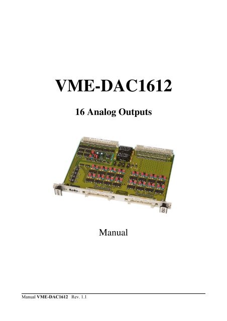
Manual VME-DAC1612 Rev. 1.1<br />
VME-DAC1612<br />
16 Analog Outputs<br />
Manual
Document file: I:\texte\Doku\MANUALS\VME\DAC1612\dac16_11.en9<br />
Date of print: 26.06.2002<br />
PCB version: VME-DAC1612 Rev. 1.0<br />
Changes in the chapters<br />
The changes in the document listed below affect changes in the hardware as well as changes in the<br />
description of facts only.<br />
Chapter Changes versus previous version<br />
4.1.2.1 Default value of base address corrected.<br />
4.1.4 Jumper unipolar/bipolar: Meaning of setting corrected.<br />
Technical details are subject to change without further notice.<br />
Manual VME-DAC1612 Rev. 1.1
Manual VME-DAC1612 Rev. 1.1<br />
N O T E<br />
The information in this document has been carefully checked and is believed to be entirely reliable. <strong>esd</strong><br />
makes no warranty of any kind with regard to the material in this document, and assumes no<br />
responsibility for any errors that may appear in this document. <strong>esd</strong> reserves the right to make changes<br />
without notice to this, or any of its <strong>product</strong>s, to improve reliability, performance or design.<br />
<strong>esd</strong> assumes no responsibility for the use of any circuitry other than circuitry which is part of a <strong>product</strong><br />
of <strong>esd</strong> gmbh.<br />
<strong>esd</strong> does not convey to the purchaser of the <strong>product</strong> described herein any license under the patent rights<br />
of <strong>esd</strong> gmbh nor the rights of others.<br />
<strong>esd</strong> electronic system design gmbh<br />
Vahrenwalder Str. 207<br />
30165 Hannover<br />
Germany<br />
Phone: +49-511-372 98-0<br />
Fax: +49-511-372 98-68<br />
E-mail: info@<strong>esd</strong>-<strong>electronics</strong>.com<br />
Internet: www.<strong>esd</strong>-<strong>electronics</strong>.com<br />
USA / Canada:<br />
<strong>esd</strong> <strong>electronics</strong> <strong>Inc</strong>.<br />
12 Elm Street<br />
Hatfield, MA 01038-0048<br />
USA<br />
Phone: +1-800-732-8006<br />
Fax: +1-800-732-8093<br />
E-mail: us-sales@<strong>esd</strong>-<strong>electronics</strong>.com<br />
Internet: www.<strong>esd</strong>-<strong>electronics</strong>.us
Contents<br />
1. Overview .................................................................... 3<br />
1.1 Module Description ......................................................... 3<br />
2. Summary of Technical Data .................................................... 4<br />
2.1 General Technical Data ...................................................... 4<br />
2.2 Technical Data of Analog Units ............................................... 5<br />
2.3 Order Information .......................................................... 6<br />
3. Address Assignment .......................................................... 7<br />
4. Jumpers and Coding Switches .................................................. 8<br />
4.1 PCB-View ................................................................ 8<br />
4.1.1 Default Setting of Jumpers ............................................. 9<br />
4.1.2 Setting Basis Address and Address Modifier Decoding ...................... 10<br />
4.1.2.1 Basis Address (Coding Switch) .................................. 10<br />
4.1.2.2 Address Modifier (J120) ....................................... 11<br />
4.1.3 Configuration of Analog Units ......................................... 13<br />
4.1.4 Mode Register (J130) ............................................... 14<br />
4.1.5 Negation of Data Bit D11 (J300) ...................................... 16<br />
4.1.6 Selecting the Output Voltage Range (J400-J731) .......................... 17<br />
5. Analog Outputs ............................................................. 19<br />
5.1 Output Circuit ............................................................ 19<br />
5.2 Operating Modes of the D/A-Converters ....................................... 20<br />
5.2.1 Data Transfer ....................................................... 20<br />
5.2.2 Unipolar Operation 0...10 V ........................................... 22<br />
5.2.3 Bipolar Operation ±5 V ............................................... 23<br />
5.2.4 Bipolar Operation ±10 V .............................................. 24<br />
5.3 Adjusting the D/A-Converters ................................................ 25<br />
5.3.1 Offset Setting ...................................................... 26<br />
5.3.2 Gain .............................................................. 27<br />
6. Software ................................................................... 29<br />
6.1 Initialisation .............................................................. 29<br />
6.2 PEARL-Example Program to Generate Lissajous-Figures on an Oscilloscope .......... 30<br />
7. Appendix ................................................................... 31<br />
7.1 Connector Assignment ..................................................... 31<br />
7.1.1 VMEbus Connector P1 ............................................... 31<br />
7.1.2 I/O-Connector P2 and Transition Module ................................ 32<br />
7.1.3 Post Connectors P800 and P801 ........................................ 34<br />
7.2 Front Panel ............................................................... 35<br />
7.3 DAC812-Adapter (DAC812-20mA) .................................. 36<br />
7.3.1 Overview .......................................................... 36<br />
7.3.2 PCB View with Jumpers .............................................. 36<br />
7.3.3 Default Settings of Jumpers ........................................... 37<br />
7.3.4 Description of Jumpers ............................................... 37<br />
7.3.5 Conversion of Voltages to Currents ..................................... 39<br />
Manual VME-DAC1612 Rev. 1.1 1
2<br />
7.3.6 Adjusting the Channels ............................................... 39<br />
7.3.7 Assignment of Connectors of the DAC812-Adapter ........................ 40<br />
7.3.7.1 Transition Connector P2 ....................................... 41<br />
7.3.7.2 Analog Outputs at P3 .......................................... 43<br />
7.3.7.3 Supplying the Analog Units via Screw Terminals (P4, P5) ............ 44<br />
7.3.7.4 Analog Outputs via Screw Terminals (P11-P18) .................... 44<br />
7.4 Circuit Diagrams of the VME-DAC1612 and DAC812-Adapter ..................... 45<br />
Manual VME-DAC1612 Rev. 1.1
1. Overview<br />
1.1 Module Description<br />
P1 VMEbus<br />
VME Address<br />
and AM<br />
Decoder Logic<br />
Mode Register<br />
VME<br />
Data Bus<br />
Driver<br />
Address, Data and Control Bus<br />
Isolator IL715<br />
DC/DC-Converter<br />
+5V<br />
±12V<br />
Electrical Isolation<br />
Digital / Analog<br />
Converter<br />
DAC 813<br />
Digital / Analog<br />
Converter<br />
DAC 813<br />
4, 8 or 16<br />
D/A-Converter Channels<br />
Digital / Analog<br />
Converter<br />
DAC 813<br />
Fig. 1.1.1: Block-circuit diagram of the VME-DAC1612 module<br />
Connector at<br />
Front Panel<br />
Overview<br />
VMEbus P2<br />
The VME-DAC1612 has got up to 16 analog outputs. The output voltages can be selected as ±5 V,<br />
±10 V or 0 ...+10 V, with a resolution of 12 bits.<br />
A D/A-converter of DAC 813 type is used. The control and data signals between VMEbus and analog<br />
process are electrically insulated by means of fast digital couplers.<br />
The power supply of the analog side (±15 V, +5 V) are generated by DC/DC-converters from the<br />
+5 VMEbus power supply.<br />
The VME-DAC1612 is compatible to VMEbus Standard Rev. C. With a height of 4 TE it uses one slot<br />
on the VMEbus.<br />
Manual VME-DAC1612 Rev. 1.1 3<br />
P800 Outputs 1...8<br />
P801 Outputs 9...16<br />
P2 Outputs 1..16
Technical Data<br />
2. Summary of Technical Data<br />
2.1 General Technical Data<br />
4<br />
VMEbus interface IEEE 1014 / C.1<br />
Data transfer mode A16/D16, A24/D16<br />
Interrupts none<br />
Temperature range max. permissible ambient temperature:<br />
0...70 C<br />
Humidity max. 90%, non-condensing<br />
Connectors P1 - DIN 41612-C96 (VMEbus)<br />
P2 - DIN 41612-C64 (analog outputs 1-16)<br />
P800 - 34-pin post connector (analog outputs 1-8)<br />
P801 - 34-pin post connector (analog outputs 9-16)<br />
X140 - 8-pin socket strip (ISP-programming for testing)<br />
Board dimensions 160 mm x 233 mm<br />
VMEbus installation 6 HE high / 4 TE wide<br />
front panel with lever holds<br />
Weight ca. 320 g<br />
Power supply VMEbus P1: 5V ± 5% / 1.6 A<br />
(typical, at T = 20 C, 16 channels)<br />
Table 2.1.1: General module data<br />
Manual VME-DAC1612 Rev. 1.1
2.2 Technical Data of Analog Units<br />
Number of D/A-channels 4, 8 or 16<br />
Resolution 12 bits<br />
D/A-converter DAC813<br />
Output voltage configurable via jumpers: 0-10 V, ±5 V, ±10 V<br />
Output capacity RL 2 k<br />
Resolution ± 1 LSB in adjusted status, i.e. *)<br />
at 0-10 V: ± 2.5 mV<br />
at ±5 V: ± 2.5 mV<br />
at ±10 V: ± 5.0 mV<br />
Settling time of D/Aconverter<br />
max. 6 s / channel<br />
(at voltage swing 20 V, final value achieved to 0.01%)<br />
Table 2.2.1: Technical data of analog units<br />
*) Note:<br />
The board is default set and adjusted to bipolar operation (±10V).<br />
Technical Data<br />
If the board is set to unipolar operation (0...10 V) via jumpers without being coordinated via the<br />
gain potentiometer afterwards, you have to consider an additional deviation of about ½ LSB<br />
(referred to maximum value).<br />
Manual VME-DAC1612 Rev. 1.1 5
Technical Data<br />
2.3 Order Information<br />
6<br />
Type Features Order no.<br />
VME-DAC1612-04 4 analog outputs, 12 bits, adjusted for ±10V V.1706.04<br />
VME-DAC1612-08 8 analog outputs, 12 bits, adjusted for ±10V V.1706.08<br />
VME-DAC1612-16 16 analog outputs, 12 bits, adjusted for ±10V V.1706.16<br />
VME-DAC1612-ADAPT1<br />
VME-DAC1612-ADAPT2<br />
DAC812-20mA-4<br />
DAC812-20mA-8<br />
Adapter module with solderless lug connectors for<br />
connection to P2<br />
Adapter module with spring clip connectors for<br />
connection to P2<br />
Adapter module for VME-DAC1612-04 to convert<br />
voltage outputs into current outputs<br />
0(4)...20 mA for 4 channels<br />
Adapter module for VME-DAC1612-08 to convert<br />
voltage outputs into current outputs<br />
0(4)...20 mA for 8 channels<br />
V.1706.09<br />
V.1706.10<br />
V.1702.24<br />
V.1702.28<br />
VME-DAC1612-OS9 C-driver for OS-9 as source code P.1706.50<br />
VME-DAC1612-VxWorks C-driver for VxWorks as source code P.1706.56<br />
VME-DAC1612-MD German <strong>manual</strong> *) V.1706.20<br />
VME-DAC1612-ME English <strong>manual</strong> *) V.1706.21<br />
*) If <strong>manual</strong> and VMEbus board are ordered together, the <strong>manual</strong> is included in the price of the board.<br />
Table 2.4.1: Order information<br />
Manual VME-DAC1612 Rev. 1.1
3. Address Assignment<br />
Address Assignment<br />
The basis address of the board is configured via the coding switches SW120...SW124. The basis<br />
address can be set in steps of 32 bytes in the 16 Mbyte address range.<br />
In addition to 'STANDARD' accesses (A24) there is the possibility to use the VME-addressing 'SHORT<br />
I/O' (jumper J120). In this addressing the address lines A16 to A23 are ignored and the basis address<br />
of the VME-DAC1612 board is set in the 'SHORT I/O' address range (64 KByte) of the VME-system.<br />
The basis address of the VME-DAC1612 is default set to $xxE20000.<br />
Each of the 16 D/A-converters of the VME-DAC1612 has got its own access address, which has to be<br />
addressed word-by-word. In addition a mode register can be read in which the setting of the operating<br />
mode and the number of equipped channels of the VME-DAC1612 is evaluated.<br />
Unit<br />
D/A-converter:<br />
DAC16<br />
DAC15<br />
DAC14<br />
DAC13<br />
DAC12<br />
DAC11<br />
DAC10<br />
DAC9<br />
D/A-converter:<br />
DAC8<br />
DAC7<br />
DAC6<br />
DAC5<br />
DAC4<br />
DAC3<br />
DAC2<br />
DAC1<br />
Offset<br />
address<br />
+ $1E<br />
+ $1C<br />
+ $1A<br />
+ $18<br />
+ $16<br />
+ $14<br />
+ $12<br />
+ $10<br />
+ $E<br />
+ $C<br />
+ $A<br />
+ $8<br />
+ $6<br />
+ $4<br />
+ $2<br />
+ $0<br />
Mode register + $0<br />
Access mode<br />
word-by-word,<br />
only writing access<br />
word-by-word,<br />
only writing access<br />
word-by-word,<br />
only reading access<br />
Table 3.1.1: Address assignment of VME-DAC1612<br />
If jumper J130/pin 1-2 is not set, the D/A-converters are selected by means of the data bits D15...D12<br />
(see page 21).<br />
Manual VME-DAC1612 Rev. 1.1 7
Jumpers and Coding Switches<br />
4. Jumpers and Coding Switches<br />
4.1 PCB-View<br />
8<br />
Fig 4.1.1: Position of coding switches and jumpers<br />
Manual VME-DAC1612 Rev. 1.1
4.1.1 Default Setting of Jumpers<br />
Jumpers and Coding Switches<br />
The according default setting at board delivery is shown in the table below.<br />
For the position of jumpers please refer to figure 4.1.1. The jumpers will be shown below as seen by<br />
users with the board in front of them and the VMEbus connectors on the right.<br />
Default setting of jumpers:<br />
Jumper Function Default setting at board delivery<br />
SW120...<br />
SW123<br />
basis address of board VME-DAC1612: $E20000<br />
J120 address modifier decoding short/standard supervisory and nonprivileged<br />
accesses permitted<br />
J130 mode register depending on model and the output voltage<br />
range selected<br />
J300 output level after RESET<br />
(negation of data bit D11 for<br />
the D/A-converters)<br />
J400, J410,<br />
J420, J430,<br />
J500, J510,<br />
J520, J530,<br />
J600, J610,<br />
J620, J630,<br />
J700, J710,<br />
J720, J730<br />
J401, J411,<br />
J421, J431,<br />
J501, J511,<br />
J521, J531,<br />
J601, J611,<br />
J621, J631,<br />
J701, J711,<br />
J721, J731<br />
voltage swing of the D/Aconverter<br />
assigned<br />
bipolar/unipolar conversion of<br />
the D/A-converter assigned<br />
D11 is inverted, i.e. a bipolar operation has<br />
been selected<br />
U = 20 V - voltage range = ±10 V<br />
bipolar : ±5V, ±10V<br />
Table 4.1.1: Default setting of jumpers<br />
Manual VME-DAC1612 Rev. 1.1 9
Jumpers and Coding Switches<br />
4.1.2 Setting Basis Address and Address Modifier Decoding<br />
4.1.2.1 Basis Address (Coding Switch)<br />
10<br />
Address<br />
bits<br />
Setting via<br />
coding switches<br />
Default setting<br />
[Hex]<br />
Position<br />
A23...A20 SW120 E on board next to VMEbus connector<br />
P1<br />
A19...A16 SW121 2<br />
A15...A12 SW122 0 in front panel (above)<br />
A11...A8 SW123 0 in front panel (below)<br />
Table 4.1.2: Setting of basis address<br />
Manual VME-DAC1612 Rev. 1.1
4.1.2.2 Address Modifier (J120)<br />
AM2 don't care<br />
Jumpers and Coding Switches<br />
The address modifiers AM0 to AM5 are <strong>complete</strong>ly evaluated on board. The signals AM3 and AM5<br />
are always decoded as '1'. The other signals can be configured via the jumper field J120. A set jumper<br />
sets the according bit to '0'.<br />
Manual VME-DAC1612 Rev. 1.1 11<br />
5<br />
J120<br />
Example shown: standard setting of address modifiers:<br />
standard supervisory data access and<br />
standard nonprivileged data access and<br />
short supervisory I/O access and<br />
short nonprivileged I/O access permitted<br />
1<br />
8<br />
2<br />
9<br />
AM0<br />
AM1<br />
AM2<br />
AM4<br />
The AM-configurations available to the VME-DAC1612 are listed in the table below. In addition to<br />
the AM-combinations listed, the bit AM2 can be ignored at decoding by setting jumper 'AM2 don't<br />
care'. Supervisor as well as nonprivileged accesses are permitted (see also example shown).<br />
CODE AM5 AM4 AM3 AM2 AM1 AM0 Function<br />
$3E 1 1 1 1 1 0<br />
standard supervisory<br />
program access<br />
$3D 1 1 1 1 0 1<br />
standard supervisory<br />
data access<br />
$3A 1 1 1 0 1 0<br />
standard nonprivileged<br />
program access<br />
$39 1 1 1 0 0 1<br />
standard nonprivileged<br />
data access<br />
$2D 1 0 1 1 0 1<br />
short supervisory<br />
I/O access<br />
$29 1 0 1 0 0 1<br />
short nonprivileged<br />
I/O access<br />
Table 4.1.3: Selectable AM-combinations
Jumpers and Coding Switches<br />
12<br />
Jumper field<br />
J120<br />
5<br />
5<br />
5<br />
5<br />
5<br />
5<br />
1<br />
8<br />
1<br />
8<br />
1<br />
8<br />
1<br />
8<br />
1<br />
8<br />
1<br />
8<br />
2<br />
9<br />
2<br />
9<br />
2<br />
9<br />
2<br />
9<br />
2<br />
9<br />
2<br />
9<br />
Jumper open<br />
Jumper closed<br />
permissible AM-codes<br />
AM5 AM4 AM3 AM2 AM1 AM0 HEX<br />
1<br />
1<br />
1<br />
1<br />
1<br />
1<br />
0<br />
1<br />
0<br />
0<br />
1<br />
1<br />
39<br />
3D<br />
addressing<br />
standard nonprivileged<br />
data access<br />
or<br />
standard supervisory<br />
data access<br />
1 1 1 1 0 1 3D standard supervisory<br />
data access<br />
1 1 1 0 0 1 39 standard nonprivileged<br />
data access<br />
1<br />
1<br />
0<br />
0<br />
1<br />
1<br />
0<br />
1<br />
0<br />
0<br />
1<br />
1<br />
29<br />
2D<br />
short nonprivileged<br />
access<br />
or<br />
short supervisory<br />
access<br />
1 0 1 1 0 1 2D short supervisory<br />
access<br />
1 0 1 0 0 1 29 short nonprivileged<br />
access<br />
Table 4.1.4: Recommended useful AM-combinations<br />
Manual VME-DAC1612 Rev. 1.1
4.1.3 Configuration of Analog Units<br />
Jumpers and Coding Switches<br />
34 jumper fields have been designed for the configuration of the board (number of channels, unipolar<br />
or bipolar operation).<br />
Via jumper field J130 the number of equipped channels and a global flag for unipolar or bipolar<br />
operation is set in the mode register.<br />
Via jumper field J300 the data bit D11 can be inverted for all D/A-converters together. This can be<br />
used, for example, to reset the D/A-converters to 0 V in bipolar operation after a RESET.<br />
Jumpers J400 to J731 switch the respective D/A-converter outputs to unipolar or bipolar operation and<br />
the desired voltage swing.<br />
Manual VME-DAC1612 Rev. 1.1 13
Jumpers and Coding Switches<br />
4.1.4 Mode Register (J130)<br />
The mode register is a 'read-only' register to configure the board via software. It is read as WORD<br />
under the local address '$00'. The LSB (D0-D7) is always read as $01. It is used to identify the board<br />
as VME-DAC1612 in the VMEbus system.<br />
The MSB contains information about the number of D/A-converter channels equipped and the polarity<br />
of the output voltage. Depending on whether the output voltage is unipolar or bipolar, the D/A-data has<br />
to be specified in the format 'Unipolar Straight Binary' or 'Binary Two's Complement'.<br />
14<br />
Register bit Assignment<br />
D15<br />
D14<br />
D13<br />
D12<br />
Number of D/A-converter channels (set via the equipment of resistors)<br />
D11 Jumper J130, pin 7-8, available for user<br />
D10 Jumper J130, pin 5-6, switching between unipolar/bipolar<br />
D9 Jumper J130, pin 3-4, reserved<br />
D8 Jumper J130, pin 1-2, DAC-addresses D12-D15/A1-A4<br />
D7 0<br />
D6 0<br />
D5 0<br />
D4 0<br />
D3 0<br />
D2 0<br />
D1 0<br />
D0 1<br />
A set jumper sets the according data bit to '0'.<br />
These bits identify the board in the VMEbus system and cannot be<br />
changed.<br />
Table 4.1.5: Jumper field J130 in mode register<br />
D8: DAC-addresses<br />
D12-D15/A1-A4... The D/A-converters of the VME-DAC1612 are usually selected via the<br />
four least significant address bits (A1...A4). If the jumper J130/pin 1-2<br />
has not been set, the D/A-converters are not selected via the addresses,<br />
but the most significant data bits (D11...D15). These bits are transmitted<br />
along with the 12-bit analog value.<br />
On the standard version of the board this jumper is default-set.<br />
Manual VME-DAC1612 Rev. 1.1
Jumpers and Coding Switches<br />
D10: unipolar/bipolar... D 10 specifies whether the D/A-converters on board have been<br />
configured for unipolar or bipolar operation. The format of the<br />
transmitted D/A-data depends on the polarity selected.<br />
Jumper J130,<br />
pin 5-6<br />
Bit D10 Polarity Data format<br />
open 0 unipolar USB (Unipolar Straight Binary)<br />
set 1 bipolar<br />
BTC (Binary Two's Complement)<br />
Default setting at delivery<br />
It is principly possible to select unipolar operation fo some channels and<br />
bipolar operation for others. However, this is not recommendable,<br />
because it does not only cause irregularities for this jumper, but also for<br />
jumper field J300. Especially the resetting of channels to 0 V after a<br />
RESET is not possible simultaneously for unipolar and bipolar<br />
operation.<br />
D11: free for users... This jumper can be freely set and evaluated by the user.<br />
D12-D15: DAC-number... By means of these four bits the number of equipped D/A-converter<br />
channels can be read. The bits encode the channel number as follows:<br />
Bit 3<br />
(D15)<br />
0<br />
0<br />
0<br />
0<br />
0<br />
0<br />
0<br />
0<br />
1<br />
1<br />
1<br />
1<br />
1<br />
1<br />
1<br />
0<br />
Bit 2<br />
(D14)<br />
0<br />
0<br />
0<br />
0<br />
1<br />
1<br />
1<br />
1<br />
0<br />
0<br />
0<br />
0<br />
1<br />
1<br />
1<br />
0<br />
Manual VME-DAC1612 Rev. 1.1 15<br />
Bit 1<br />
(D13)<br />
0<br />
0<br />
1<br />
1<br />
0<br />
0<br />
1<br />
1<br />
0<br />
0<br />
1<br />
1<br />
0<br />
0<br />
1<br />
0<br />
Bit 0<br />
(D12)<br />
1<br />
0<br />
1<br />
0<br />
1<br />
0<br />
1<br />
0<br />
1<br />
0<br />
1<br />
0<br />
1<br />
0<br />
1<br />
0<br />
Number of equipped D/A-converter<br />
channels<br />
Table 4.1.6: Encoding the number of equipped D/A-converter<br />
channels<br />
1<br />
2<br />
3<br />
4<br />
5<br />
6<br />
7<br />
8<br />
9<br />
10<br />
11<br />
12<br />
13<br />
14<br />
15<br />
16
Jumpers and Coding Switches<br />
4.1.5 Negation of Data Bit D11 (J300)<br />
Via jumper field J300 the data bit D11 can be inverted for all D/A-converters simultaneously. This is<br />
necessary, because depending on the mode of the output voltage, the D/A-converters expect the data<br />
in various formats:<br />
16<br />
In unipolar operation the data has to be transmitted in USB (Unipolar Straight Binary)<br />
format.<br />
In bipolar operation the converter expects the data in BTC (Binary Two's Complement)<br />
format.<br />
Attention:<br />
The negation is especially important, because the analog outputs will only be set to 0 V after a<br />
RESET, if bit D11 has got the level required for the operating mode!<br />
jumper open jumper closed<br />
1 unipolar operation (D11 not inverted)<br />
2<br />
3<br />
J300<br />
bipolar operation (D11 inverted)<br />
Example: D11 inverted for bipolar operation of D/A-converter outputs<br />
Manual VME-DAC1612 Rev. 1.1
4.1.6 Selecting the Output Voltage Range (J400-J731)<br />
Jx1<br />
3<br />
2<br />
1<br />
Jx0<br />
2<br />
1<br />
Jx1<br />
3<br />
2<br />
1<br />
Jx0<br />
2<br />
1<br />
unipolar output voltage<br />
bipolar output voltage<br />
open:<br />
closed:<br />
voltage swing = 20 V<br />
voltage swing = 10 V<br />
Jumpers and Coding Switches<br />
For each analog channel there are two jumper fields to configure the voltage range. As the jumpers are<br />
closely connected, they will be explained together.<br />
The voltage swing of the A/D-converters is set via jumpers J400...J730. Unipolar and bipolar operations<br />
are selected by means of the three-pin jumper fields J401...J731. For the assignment of jumpers to the<br />
sixteen channels, please refer to the PCB view on page 8. There the channel units are designated by<br />
numbers.<br />
Alternatively, the voltage swing can also be determined by equipping resistors. In that case the jumpers<br />
are not equipped.<br />
Example: Unipolar output voltage 0...+10V<br />
Jumper settings for output voltage ranges<br />
Output voltage range<br />
0...+10V<br />
Default setting at<br />
delivery ->><br />
It is also important to make sure that the correct output<br />
Output voltage range<br />
±5V<br />
Manual VME-DAC1612 Rev. 1.1 17<br />
Jx1<br />
3<br />
2<br />
1<br />
Jx0<br />
2<br />
1<br />
output voltage range<br />
±10V<br />
Jx1<br />
3<br />
2<br />
1<br />
Jx0<br />
2<br />
1<br />
jumper open jumper closed
Jumpers and Coding Switches<br />
configuration has been set in mode register via BR1 and that the correct polarity has been assigned to<br />
data bit D11 via BR7!<br />
Note:<br />
Principally, unipolar and bipolar output configurations can be selected on a VME-DAC1612. However,<br />
this is not recommendable, because other settings (at J130) are made simultaneously for all channels<br />
of the board.<br />
The jumpers are assigned to output channels as follows:<br />
18<br />
Jumper for voltage swing Jumper for polarity Output channel<br />
J400<br />
J410<br />
J420<br />
J430<br />
J500<br />
J510<br />
J520<br />
J530<br />
J600<br />
J610<br />
J620<br />
J630<br />
J700<br />
J710<br />
J720<br />
J730<br />
J401<br />
J411<br />
J421<br />
J431<br />
J501<br />
J511<br />
J521<br />
J531<br />
J601<br />
J611<br />
J621<br />
J631<br />
J701<br />
J711<br />
J721<br />
J731<br />
Table 4.1.7: Assignment of jumpers BR8 to BR23 to output channels<br />
Note:<br />
For the assignment of jumpers to the sixteen channels, please refer to the PCB view on page 8. There<br />
the channel circuits are designated by numbers.<br />
1<br />
2<br />
3<br />
4<br />
5<br />
6<br />
7<br />
8<br />
9<br />
10<br />
11<br />
12<br />
13<br />
14<br />
15<br />
16<br />
Manual VME-DAC1612 Rev. 1.1
5. Analog Outputs<br />
5.1 Output Circuit<br />
Fig. 5.1.1: Output circuit of the VME-DAC1612 (example: channel 1)<br />
Analog Outputs<br />
Manual VME-DAC1612 Rev. 1.1 19
Analog Outputs<br />
5.2 Operating Modes of the D/A-Converters<br />
5.2.1 Data Transfer<br />
Each of the 16 D/A-converters of the VME-DAC1612 has got its own access address. Writing the data<br />
at this address sets the D/A-converters und starts the conversion. The data has to be transferred word<br />
by word, because the conversion is started immediately when the WRITE signal is cancelled!<br />
Additionally, a mode register can be read in which the setting of the output polarity and the number of<br />
equipped channels can be evaluated. The mode register has already been described in the chapter<br />
‘Mode Register (J130)’ on page 14.<br />
The D/A-converters evaluate the received data word as follows:<br />
D15 D14 D13 D12 D11 D10 D9 D8 D7 D6 D5 D4 D3 D2 D1 D0<br />
20<br />
x x x x f<br />
MSB<br />
Meaning of bits:<br />
f f f f f f f f f f f<br />
LSB<br />
D/A-converter data (f f f f .f f f f .f f f f)<br />
Data bit D11 can be inverted for all D/A-converters simultaneously by means of jumper J300.<br />
This is necessary if the outputs are run in bipolar mode, because the D/A-converters expect the<br />
data in various formats, depending on the operating mode:<br />
In unipolar operation the data have to be specified in<br />
USB (Unipolar Straight Binary) format.<br />
In bipolar operation the converter expects the data in<br />
BTC (Binary Two's Complement) format.<br />
Attention!<br />
The negation is especially important, because the analog outputs will only be set to 0 V<br />
following a RESET, if bit D11 has got the level required for this operating mode!<br />
In mixed operation of bipolar and unipolar channels on the VME-DAC1612 it is up to the user<br />
to decide which channels are to be set to 0 V after a RESET*.<br />
In the following chapters the voltage values corresponding to the binary data words of the<br />
respective operating mode will be shown.<br />
Manual VME-DAC1612 Rev. 1.1
Analog Outputs<br />
Alternative channel selection (xxxx)<br />
These bits (D15...D12) are not evaluated, unless jumper J130/pin 1-2 is not set (‘1’). In this case<br />
the desired D/A-converter is selected via these bits:<br />
Value of bits D/A-converter<br />
(output channel)<br />
D15 D14 D13 D12<br />
0<br />
0<br />
0<br />
0<br />
0<br />
0<br />
0<br />
0<br />
0<br />
1<br />
1<br />
1<br />
1<br />
1<br />
1<br />
1<br />
0<br />
0<br />
0<br />
0<br />
0<br />
1<br />
1<br />
1<br />
1<br />
0<br />
0<br />
0<br />
0<br />
1<br />
1<br />
1<br />
0<br />
0<br />
0<br />
1<br />
1<br />
0<br />
0<br />
1<br />
1<br />
0<br />
0<br />
1<br />
1<br />
0<br />
0<br />
1<br />
0<br />
1<br />
0<br />
1<br />
0<br />
1<br />
0<br />
1<br />
0<br />
1<br />
0<br />
1<br />
0<br />
1<br />
0<br />
1<br />
Table 5.2.1: Selection of D/A-converter<br />
If jumper J130/pin 1-2 is set (‘0’), the D/A-converters are selected via addresses A1...A4, as<br />
described on page 7.<br />
Manual VME-DAC1612 Rev. 1.1 21<br />
1<br />
2<br />
3<br />
4<br />
5<br />
6<br />
7<br />
8<br />
9<br />
10<br />
11<br />
12<br />
13<br />
14<br />
15<br />
16
Analog Outputs<br />
5.2.2 Unipolar Operation 0...10 V<br />
Prerequisite for a unipolar operation with 0...10 V is the correct configuration of the board via the<br />
jumpers (J300 for all channels together and two of jumpers J400...J731 for the according channel)!<br />
For the output voltage range 0...10V the converter components DAC813 require the data in format<br />
'USB' (Unipolar Straight Binary). The following table shows the assignment of data to output voltages<br />
for this format by means of some basic data.<br />
22<br />
Input<br />
D11 D0<br />
MSB LSB<br />
<br />
Output<br />
111111111111 + maximum value (+ 9.9976 V)<br />
100000000000 + ½ maximum value (+ 5.0000 V)<br />
011111111111 + ½ maximum value-1 LSB (+ 4.9976 V)<br />
000000000000 null ( 0.0000 V)<br />
Table 5.2.2: Data format for output voltages of 0...10 V<br />
Manual VME-DAC1612 Rev. 1.1
5.2.3 Bipolar Operation ±5 V<br />
Analog Outputs<br />
Prerequisite for a bipolar operation with ±5 V is the correct configuration of the board via the jumpers<br />
(J300 for all channels together and two of jumpers J400...J731 for the according channel)!<br />
For the output voltage range ±5 V the converter components DAC813 require the data in 'BTC' (Binary<br />
Two's Complement) format. The following table shows the assignment of data to output voltages for<br />
this format by means of some basic data.<br />
Input<br />
D11 D0<br />
MSB LSB<br />
<br />
Output<br />
111111111111 - 1 LSB (- 0.0024 V)<br />
100000000000 - maximum value (- 5.000 V)<br />
011111111111 + maximum value (+ 4.9975 V)<br />
000000000000 null (0.0000 V)<br />
Table 5.2.3: Data format for output voltages of ±5 V<br />
Manual VME-DAC1612 Rev. 1.1 23
Analog Outputs<br />
5.2.4 Bipolar Operation ±10 V<br />
Prerequisite for a bipolar operation with ±10 V is the correct configuration of the board via the jumpers<br />
(J300 for all channels together and two of jumpers J300...J731 for the according channel)!<br />
For the output voltage range ±10 V the converter components DAC813 require the data in 'BTC'<br />
(Binary Two's Complement) format. The following table shows the assignment of data to output<br />
voltages for this format by means of some basic data.<br />
24<br />
Input<br />
D11 D0<br />
MSB LSB<br />
<br />
Output<br />
111111111111 - 1 LSB (- 0.0049 V)<br />
100000000000 - maximum value (- 10.0000 V)<br />
011111111111 + maximum value (+ 9.9951 V)<br />
000000000000 null (0.0000 V)<br />
Table 5.2.4: Data format for output voltages of ±10 V<br />
Manual VME-DAC1612 Rev. 1.1
5.3 Adjusting the D/A-Converters<br />
Px2<br />
Px1<br />
Px0<br />
Offset bipolar output voltage<br />
Analog Outputs<br />
Offset and Gain have already been adjusted by the manufacturer. However, if another adjustment, for<br />
instance following a change in operating mode of a channel, was required, just follow the instructions<br />
given in the following chapters.<br />
Note:<br />
For the assignment of potentiometers to the sixteen channels please refer to the PCB view on page 8.<br />
There the channel circuits are designated by numbers.<br />
For each channel three potentiometers are available for adjustment:<br />
Offset unipolar output voltage<br />
The following table shows the potentiometers for Offset (unipolar and bipolar) and Gain for each D/Achannel.<br />
D/A-converter<br />
channel<br />
1<br />
2<br />
3<br />
4<br />
5<br />
6<br />
7<br />
8<br />
9<br />
10<br />
11<br />
12<br />
13<br />
14<br />
15<br />
16<br />
Gain<br />
P400<br />
P410<br />
P420<br />
P430<br />
P500<br />
P510<br />
P520<br />
P530<br />
P600<br />
P610<br />
P620<br />
P630<br />
P700<br />
P710<br />
P720<br />
P730<br />
Manual VME-DAC1612 Rev. 1.1 25<br />
Gain<br />
Potentiometer<br />
Offset<br />
bipolar<br />
P401<br />
P411<br />
P421<br />
P431<br />
P501<br />
P511<br />
P521<br />
P531<br />
P601<br />
P611<br />
P621<br />
P631<br />
P701<br />
P711<br />
P721<br />
P731<br />
Offset<br />
unipolar<br />
P402<br />
P412<br />
P422<br />
P432<br />
P502<br />
P512<br />
P522<br />
P532<br />
P602<br />
P612<br />
P622<br />
P632<br />
P702<br />
P712<br />
P722<br />
P732<br />
Table 5.3.1: Assignment of adjusting potentiometers to channels
Analog Outputs<br />
5.3.1 Offset Setting<br />
The offset voltage is adjusted by means of a potentiometer (see above). Via this adjustment the offset<br />
voltage of the D/A-converter and the following operation amplifier is set.<br />
In unipolar operation the value $0000 is applied to the D/A-converter which is to generate an output<br />
voltage of 0.0 V at the output of the according channel of the VME-DAC1612.<br />
26<br />
$0000 - 0.0 V<br />
Via offset potentiometer ‘Px2’ the output of the respective channel is set to 0.0 V.<br />
In bipolar operation (BTC) the value $0800 is applied to the D/A-converter which is to generate the<br />
maximum possible negative output voltage.<br />
$0800 - -5.0 V or -10.0 V<br />
Via offset potentiometer ‘Px1’ the output of the respective channel is set to the maximum possible<br />
negative output voltage (-5.0 V or -10.0 V).<br />
Manual VME-DAC1612 Rev. 1.1
5.3.2 Gain<br />
Analog Outputs<br />
For unipolar as well as for bipolar operation a digital value is applied to the D/A-converter which<br />
generates the maximum possible positive output voltage:<br />
$0FFF = +9.9976 V in unipolar operation<br />
or $07FF = +4.9976 V or +9.9951 V in bipolar operation<br />
Via gain potentiometer ‘Px0’ the output of the respective channel is set to the maximum possible<br />
positive output voltage.<br />
Note:<br />
The board is first configured and adjusted to the unipolar operation by the manufacturer. Then it is<br />
configured and adjusted to bipolar operation. The board is delivered with the bipolar setting (±10<br />
V).<br />
If the board is then changed to unipolar operation (0...10 V) via jumpers again and is then not<br />
adjusted via the gain potentiometer, you have to expect a further deviation of about ½ LSB<br />
(regarding to the maximum value) in unipolar operation.<br />
Manual VME-DAC1612 Rev. 1.1 27
Analog Outputs<br />
28<br />
This side is intentionally left blank.<br />
Manual VME-DAC1612 Rev. 1.1
6. Software<br />
6.1 Initialisation<br />
Software<br />
The D/A-converter outputs generally do not have to be especially initialized after a RESET signal by<br />
the VMEbus, if the same operating mode was selected for all output channels. In this case a sequence<br />
control on board resets the output voltages to 0.0 V.<br />
In mixed operation (unipolar and bipolar) the reset status for only one operating mode is met, however,<br />
so that the other channels should be reset by the user.<br />
An output voltage at the D/A-converter channel can be generated by writing the data word word-byword<br />
(depending on operating mode) at the corresponding address of the DAC channel.<br />
The following page shows an example program for accesses to the VME-DAC1612 board in realtimemultitasking-standard<br />
language PEARL.<br />
The MODE register can only be read (see chapter ‘Mode Register (J130)’, page 14 ), from which the<br />
user can take information about the configuration of the VME-DAC1612-board in the system.<br />
Manual VME-DAC1612 Rev. 1.1 29
Software<br />
6.2 PEARL-Example Program to Generate Lissajous-Figures on an Oscilloscope<br />
MODULE DAC812;<br />
SYSTEM;<br />
/* für 'xx' jeweils VMEbus Adresse einsetzen */<br />
dac0 : BU(xxE20000,02) ->; /* DA-Wandler Nr. 1 */<br />
dac1 : BU(xxE20002,02) ->; /* DA-Wandler Nr. 2 */<br />
dac2 : BU(xxE20004,02) ->; /* DA-Wandler Nr. 3 */<br />
dac3 : BU(xxE20006,02) ->; /* DA-Wandler Nr. 4 */<br />
dac4 : BU(xxE20008,02) ->; /* DA-Wandler Nr. 5 */<br />
dac5 : BU(xxE2000A,02) ->; /* DA-Wandler Nr. 6 */<br />
dac6 : BU(xxE2000C,02) ->; /* DA-Wandler Nr. 7 */<br />
dac7 : BU(xxE2000E,02) ->; /* DA-Wandler Nr. 8 */<br />
dacmode: BU(xxE20000,02)
7. Appendix<br />
7.1 Connector Assignment<br />
7.1.1 VMEbus Connector P1<br />
Pin Row a Row b Row c<br />
1<br />
2<br />
3<br />
4<br />
5<br />
6<br />
7<br />
8<br />
9<br />
10<br />
11<br />
12<br />
13<br />
14<br />
15<br />
16<br />
17<br />
18<br />
19<br />
20<br />
21<br />
22<br />
23<br />
24<br />
25<br />
26<br />
27<br />
28<br />
29<br />
30<br />
31<br />
32<br />
D00<br />
D01<br />
D02<br />
D02<br />
D04<br />
D05<br />
D06<br />
D07<br />
GND<br />
-<br />
GND<br />
DS1*<br />
DS0*<br />
WRITE*<br />
GND<br />
DTACK*<br />
GND<br />
AS*<br />
GND<br />
IACK*<br />
IACKIN* ,<br />
IACKOUT* -<br />
AM4<br />
-<br />
-<br />
-<br />
A04<br />
A03<br />
A02<br />
A01<br />
-<br />
+5V<br />
-<br />
-<br />
-<br />
BG0IN* ,<br />
BG0OUT* -<br />
BG1IN* ,<br />
BG1OUT* -<br />
BG2IN* ,<br />
BG2OUT* -<br />
BG3IN* ,<br />
BG3OUT* -<br />
-<br />
-<br />
-<br />
-<br />
AM0<br />
AM1<br />
AM2<br />
AM3<br />
GND<br />
-<br />
-<br />
GND<br />
-<br />
-<br />
-<br />
-<br />
-<br />
-<br />
-<br />
-<br />
+5V<br />
D08<br />
D09<br />
D10<br />
D11<br />
D12<br />
D13<br />
D14<br />
D15<br />
GND<br />
-<br />
-<br />
SYSRESET*<br />
LWORD*<br />
AM5<br />
A23<br />
A22<br />
A21<br />
A20<br />
A19<br />
A18<br />
A17<br />
A16<br />
A15<br />
A14<br />
A13<br />
A12<br />
A11<br />
A10<br />
A09<br />
A08<br />
-<br />
+5V<br />
Spring contact strip according to DIN41612 design C96/a+b+c<br />
Imax per pin : 1.0 A<br />
,<br />
-... signals on board bridged<br />
- ... signal not connected<br />
Appendix<br />
Manual VME-DAC1612 Rev. 1.1 31
Appendix<br />
7.1.2 I/O-Connector P2 and Transition Module<br />
32<br />
Pin<br />
2<br />
4<br />
6<br />
8<br />
10<br />
12<br />
14<br />
16<br />
18<br />
20<br />
22<br />
24<br />
26<br />
28<br />
30<br />
32<br />
34<br />
36<br />
38<br />
40<br />
42<br />
44<br />
46<br />
48<br />
50<br />
52<br />
54<br />
56<br />
58<br />
60<br />
62<br />
64<br />
Assignment of a 64-pin transition module<br />
Assignment of I/O-connector P2<br />
Row a Signal Row c<br />
1<br />
2<br />
3<br />
4<br />
5<br />
6<br />
7<br />
8<br />
9<br />
10<br />
11<br />
12<br />
13<br />
14<br />
15<br />
16<br />
17<br />
18<br />
19<br />
20<br />
21<br />
22<br />
23<br />
24<br />
25<br />
26<br />
27<br />
28<br />
29<br />
30<br />
31<br />
32<br />
-<br />
-<br />
DAC4-GND<br />
-<br />
DAC8-GND<br />
-<br />
DAC3-GND<br />
-<br />
DAC7-GND<br />
-<br />
DAC2-GND<br />
-<br />
DAC6-GND<br />
-<br />
DAC1-GND<br />
-<br />
DAC5-GND<br />
-<br />
DAC12-GND<br />
DAC16-GND<br />
DAC11-GND<br />
DAC15-GND<br />
DAC10-GND<br />
DAC14-GND<br />
DAC09-GND<br />
DAC13-GND<br />
-<br />
(+5 V analog)<br />
(-15 V analog)<br />
(+15 V analog)<br />
GND analog<br />
-<br />
-<br />
-<br />
DAC4-OUT<br />
-<br />
DAC8-OUT<br />
-<br />
DAC3-OUT<br />
-<br />
DAC7-OUT<br />
-<br />
DAC2-OUT<br />
-<br />
DAC6-OUT<br />
-<br />
DAC1-OUT<br />
-<br />
DAC5-OUT<br />
-<br />
DAC12-OUT<br />
DAC16-OUT<br />
DAC11-OUT<br />
DAC15-OUT<br />
DAC10-OUT<br />
DAC14-OUT<br />
DAC9-OUT<br />
DAC13-OUT<br />
-<br />
(+5 V analog)<br />
(-15 V analog)<br />
(+15 V analog)<br />
GND analog<br />
-<br />
I/O-connector: spring contact strip according to DIN41612 design C64/a+c<br />
Imax per pin : 1.0 A<br />
See the following page for the description of signals.<br />
1<br />
2<br />
3<br />
4<br />
5<br />
6<br />
7<br />
8<br />
9<br />
10<br />
11<br />
12<br />
13<br />
14<br />
15<br />
16<br />
17<br />
18<br />
19<br />
20<br />
21<br />
22<br />
23<br />
24<br />
25<br />
26<br />
27<br />
28<br />
29<br />
30<br />
31<br />
32<br />
Pin<br />
1<br />
3<br />
5<br />
7<br />
9<br />
11<br />
13<br />
15<br />
17<br />
19<br />
21<br />
23<br />
25<br />
27<br />
29<br />
31<br />
33<br />
35<br />
37<br />
39<br />
41<br />
43<br />
45<br />
47<br />
49<br />
51<br />
53<br />
55<br />
57<br />
59<br />
61<br />
63<br />
Manual VME-DAC1612 Rev. 1.1
Signal descriptions for `I/O-connector P2 and transition module’:<br />
- ... These connector pins are not connected on board.<br />
DACx-OUT ... Output of A/D-converter channel 'x' (x = 1, 2, ...16)<br />
DACx-GND ... reference potential of A/D-converter output 'x'<br />
(+5V analog), (+15V analog),<br />
(-15V analog)<br />
Appendix<br />
Attention!<br />
In the standard version of the board the analog supply voltages are<br />
generated via DC/DC-converters from the +5V-power supply of the<br />
VMEbus.<br />
The supply voltages (+5V analog), (+15V analog) and (-15V analog) are not<br />
connected, therefore!<br />
GND analog ... The reference potential of the analog supply voltages is only required at<br />
P2, if the DAC812 adapter is used for the conversion of voltage outputs<br />
to current outputs.<br />
The reference potential of the analog supply voltages is connected to the<br />
reference potentials of the analog outputs only on the VME-DAC1612<br />
board and not on the adapter. Therefore the reference potential of the<br />
supply voltages of the VME-DAC1612 and the reference potential of the<br />
supply voltages of the adapter board (GND analog ) are connected via P2.<br />
Manual VME-DAC1612 Rev. 1.1 33
Appendix<br />
7.1.3 Post Connectors P800 and P801<br />
34<br />
Signal<br />
Pin<br />
P801<br />
Signal<br />
DAC9-GND 1 2 DAC9-OUT<br />
DAC9-GND 3 4 -<br />
DAC10-GND 5 6 DAC10-OUT<br />
DAC10-GND 7 8 -<br />
DAC11-GND 9 10 DAC11-OUT<br />
DAC11-GND 11 12 -<br />
DAC12-GND 13 14 DAC12-OUT<br />
DAC12-GND 15 16 -<br />
DAC13-GND 17 18 DAC13-OUT<br />
DAC13-GND 19 20 -<br />
DAC14-GND 21 22 DAC14-OUT<br />
DAC14-GND 23 24 -<br />
DAC15-GND 25 26 DAC15-OUT<br />
DAC15-GND 27 28 -<br />
DAC16-GND 29 30 DAC16-OUT<br />
DAC16-GND 31 32 -<br />
Shield 33 34 Shield<br />
Signal<br />
Pin<br />
P800<br />
Signal<br />
DAC1-GND 1 2 DAC1-OUT<br />
DAC1-GND 3 4 -<br />
DAC2-GND 5 6 DAC2-OUT<br />
DAC2-GND 7 8 -<br />
DAC3-GND 9 10 DAC3-OUT<br />
DAC3-GND 11 12 -<br />
DAC4-GND 13 14 DAC4-OUT<br />
DAC4-GND 15 16 -<br />
DAC5-GND 17 18 DAC5-OUT<br />
DAC5-GND 19 20 -<br />
DAC6-GND 21 22 DAC6-OUT<br />
DAC6-GND 23 24 -<br />
DAC7-GND 25 26 DAC7-OUT<br />
DAC7-GND 27 28 -<br />
DAC8-GND 29 30 DAC8-OUT<br />
DAC8-GND 31 32 -<br />
Shield 33 34 Shield<br />
34-pin post connector in front panel with locking.<br />
Please refer to previous page for a description of signals.<br />
Manual VME-DAC1612 Rev. 1.1
7.2 Front Panel<br />
LED 'Busy' (yellow):<br />
- On, if VMEbus has access to<br />
the board<br />
Coding switch SW122:<br />
- Adress bits A12...A15<br />
Coding switch SW123:<br />
- Adress bits A8...A11<br />
Post connector P801:<br />
- Analog outputs 9...16<br />
Post connector P800:<br />
- Analog outputs 1...8<br />
DAC1612<br />
Appendix<br />
Manual VME-DAC1612 Rev. 1.1 35<br />
BUSY<br />
ADR<br />
A<br />
15<br />
:<br />
12<br />
11<br />
:<br />
8<br />
16<br />
D<br />
A<br />
C<br />
O<br />
U<br />
T<br />
9<br />
8<br />
D<br />
A<br />
C<br />
O<br />
U<br />
T<br />
1
Appendix<br />
7.3 DAC812-Adapter (DAC812-20mA)<br />
7.3.1 Overview<br />
The optional adapter DAC812-20mA is connected to I/O-connector P2. The adapter converts the output<br />
voltage of 0...10 V to a current of 0(4)...20 mA. You can select between 0...20 mA and 4...20 mA via<br />
a jumper. When using a precision load resistor at the current output, the voltage drop caused by the<br />
connected line can be compensated: if, for instance, a resistor of 500 is connected to the output<br />
configured for 0...20 mA, the voltage drop over the resistor is always 0...10 V.<br />
The conversion from voltage/current is made via converter component XTR110 by means of a<br />
transistor (BSS110), connected in series. Potentiometers for adjusting offset and gain are available for<br />
each of the at most 8 channels. The channels have already been adjusted by the manufacturer.<br />
Each of the voltage/current converters has got three jumpers, by which the three different operating<br />
modes can be selected:<br />
1. Voltage output (the output voltage of the VME-DAC1612 is directly fed to the terminals<br />
of the adapter. All voltage ranges of the VME-DAC1612 are permissible)<br />
2. Current output 0...20 mA<br />
3. Current output 4...20 mA (line break recognition)<br />
7.3.2 PCB View with Jumpers<br />
36<br />
Fig. 7.3.1: Position of jumpers on the DAC812-adapter<br />
Manual VME-DAC1612 Rev. 1.1
7.3.3 Default Settings of Jumpers<br />
Appendix<br />
The respective default setting at the time of delivery of the board can be found in the table below.<br />
The position of jumpers can be found in figure 7.3.1. The jumpers are shown below as seen by users<br />
with the board in front of them, transition connector P2 pointing to the left.<br />
Jumper Function Default setting at the<br />
time of delivery<br />
BR11, BR21,...<br />
...BR81<br />
BR12, BR22,...<br />
...BR82<br />
BR13, BR23,...<br />
...BR83<br />
7.3.4 Description of Jumpers<br />
Selection between 0...20 mA and 4...20 mA all channels set to<br />
0...20 mA<br />
Selection between current and voltage output all channels set to<br />
current output<br />
Determining the reference input of the<br />
voltage/current converters for 0...20 mA or<br />
4...20 mA<br />
Table 7.3.1: Default setting of jumpers<br />
set to 0...20 mA for all<br />
channels<br />
Each channel of the DAC812-adapter has got three jumper fields. By means of bridges Brx1 and Brx3<br />
(x= 1, 2,..., 8 for the channel number) 0...20 mA and 4...20 mA current outputs are distinguished.<br />
Jumper Brx2 distinguishes between voltage and current output.<br />
Channel No. Current or voltage<br />
output<br />
1<br />
2<br />
3<br />
4<br />
5<br />
6<br />
7<br />
8<br />
BR12<br />
BR22<br />
BR32<br />
BR42<br />
BR52<br />
BR62<br />
BR72<br />
BR82<br />
0...20 mA or 4...20 mA<br />
output<br />
BR11 and BR13<br />
BR21 and BR23<br />
BR31 and BR33<br />
BR41 and BR43<br />
BR51 and BR53<br />
BR61 and BR63<br />
BR71 and BR73<br />
BR81 and BR83<br />
Table 7.3.2: Assignment of jumpers to channels<br />
Manual VME-DAC1612 Rev. 1.1 37
Appendix<br />
There are three combinations of jumper positions. They are shown in the following figures. The<br />
example in the diagrams always shows the first channel in the possible configurations. The position<br />
of the jumpers of the individual channels can be taken from the figure 'Position of jumpers of the<br />
DAC812-adapter' above.<br />
BR11<br />
OFS<br />
GAIN<br />
BR11<br />
OFS<br />
GAIN<br />
38<br />
BR11<br />
OFS<br />
GAIN<br />
0 4<br />
1 2 3<br />
100k<br />
100k<br />
47K<br />
22R<br />
0 4<br />
1 2 3<br />
100k<br />
100k<br />
47K<br />
22R<br />
U1<br />
XTR 110<br />
U1<br />
XTR 110<br />
1<br />
2<br />
BR12<br />
3<br />
4<br />
1<br />
BR13<br />
2<br />
Fig. 7.3.2: Jumper position for voltage outputs<br />
0 4<br />
1 2 3<br />
1<br />
2<br />
BR12<br />
3<br />
4<br />
1<br />
BR13<br />
2<br />
Fig. 7.3.3: Jumper position for 0...20 mA current outputs.<br />
100k<br />
100k<br />
47K<br />
22R<br />
U1<br />
XTR 110<br />
1<br />
2<br />
BR12<br />
3<br />
4<br />
1<br />
BR13<br />
2<br />
Fig. 7.3.4: Jumper position for 4...20 mA current outputs<br />
Description of jumper symbol:<br />
Voltage outputs<br />
If the output voltage of the VME-DAC1612 is to fed through for<br />
a channel, a jumper has to bridge pins 2-3 in jumper field Brx2.<br />
Jumper fields Brx1 and Brx2 are insignificant in this case.<br />
(x = 1, 2,...,8 for the channel number).<br />
0...20 mA current outputs<br />
For current outputs pins 1-2 and 3-4 of jumper field BRx2 have to<br />
be bridged. For operation with 0...20 mA a jumper has to be set on<br />
pins 1-2 of jumper field Brx1 and jumper Brx3 has to be set<br />
additionally.<br />
(x = 1, 2,...,8 for the channel number).<br />
4...20 mA current outputs<br />
For current outputs pins 1-2 and 3-4 of jumper field BRx2<br />
have to be bridged. For operation with 4...20 mA you also<br />
have to bridge pins 2-3 of jumper field Brx1. Jumper Brx3<br />
remains open.<br />
(x = 1, 2,...,8 for the channel number).<br />
Jumper open<br />
Jumper closed<br />
Manual VME-DAC1612 Rev. 1.1
7.3.5 Conversion of Voltages to Currents<br />
The conversion of output voltage to current outputs is shown in the table below:<br />
VME-DA1612-output<br />
voltage [V]<br />
+ 0.0<br />
+ 0.0 (4 mA option)<br />
+ 9.9975<br />
7.3.6 Adjusting the Channels<br />
Output current of the DAC812-20mA adapter<br />
[mA]<br />
+ 0.0<br />
+ 4.0<br />
+ 20.0<br />
Table 7.3.3: Voltage/current assignment<br />
Appendix<br />
Offset and Gain have already been adjusted by the manufacturer. If you require another adjustment,<br />
for instance following a change in the operating mode of a channel, please refer to the previous chapter<br />
'Adjusting the D/A-Converters'. Instead of the voltage values cited there, you set the equivalent current<br />
values.<br />
If you only feed through the output voltage of the VME-DAC1612, you do not have to adjust offset and<br />
gain.<br />
Manual VME-DAC1612 Rev. 1.1 39
Appendix<br />
7.3.7 Assignment of Connectors of the DAC812-Adapter<br />
In addition to the 64-pin socket strip P2 the adapter has got a 10-pin post connector (P3) to connect the<br />
analog outputs via flat ribbon cable and it has got screw terminals to connect the analog supply voltages<br />
(P4, P5).<br />
The analog outputs can also be connected via screw-type terminals (such as PHOENIX SMKDS1.2-3)<br />
(P11-P18). These connectors are not available in the standard version of the adapter. If required, they<br />
can be equipped afterwards by the user or the manufacturer, if desired.<br />
If connectors P11 to P18 are not required, the adapter board can be sawn-off at the line especially<br />
marked. This is useful, if the space in the VMEbus system is limited. The length of the board is reduced<br />
from 132 mm to 81.5 mm. Please refer to figure 'Position of jumpers of the DAC812-adapter' above<br />
for the position of the line.<br />
40<br />
Manual VME-DAC1612 Rev. 1.1
7.3.7.1 Transition Connector P2<br />
Assignment of I/O-connector P2<br />
Row a Signal Row c<br />
1<br />
2<br />
3<br />
4<br />
5<br />
6<br />
7<br />
8<br />
9<br />
10<br />
11<br />
12<br />
13<br />
14<br />
15<br />
16<br />
17<br />
18<br />
19<br />
20<br />
21<br />
22<br />
23<br />
24<br />
25<br />
26<br />
27<br />
28<br />
29<br />
30<br />
31<br />
32<br />
Signal-GND<br />
.<br />
.<br />
.<br />
.<br />
.<br />
.<br />
.<br />
.<br />
.<br />
.<br />
.<br />
.<br />
.<br />
.<br />
.<br />
Signal-GND<br />
-<br />
-<br />
-<br />
-<br />
-<br />
-<br />
-<br />
-<br />
-<br />
-<br />
+5 V analog<br />
-15 V analog<br />
+15 V analog<br />
GND analog<br />
-<br />
-<br />
-<br />
DAC4-IN<br />
-<br />
DAC8-IN<br />
-<br />
DAC3-IN<br />
-<br />
DAC7-IN<br />
-<br />
DAC2-IN<br />
-<br />
DAC6-IN<br />
-<br />
DAC1-IN<br />
-<br />
DAC5-IN<br />
-<br />
-<br />
-<br />
-<br />
-<br />
-<br />
-<br />
-<br />
-<br />
-<br />
+5 V analog<br />
-15 V analog<br />
+15 V analog<br />
GND analog<br />
-<br />
I/O-connector: Spring contact strip in accordance with DIN41612 design C64/a+c<br />
Imax per pin : 1.0 A<br />
For signal description turn to the following page.<br />
Appendix<br />
Manual VME-DAC1612 Rev. 1.1 41<br />
1<br />
2<br />
3<br />
4<br />
5<br />
6<br />
7<br />
8<br />
9<br />
10<br />
11<br />
12<br />
13<br />
14<br />
15<br />
16<br />
17<br />
18<br />
19<br />
20<br />
21<br />
22<br />
23<br />
24<br />
25<br />
26<br />
27<br />
28<br />
29<br />
30<br />
31<br />
32
Appendix<br />
Signal descriptions to `Transition Connector P2`:<br />
- ... these connector pins are not connected on board<br />
DACx-IN ... analog input signal of the DAC812-adapter board<br />
(= output of VME-DAC1612 with x = 1...8)<br />
Signal-GND ... reference potential of analog inputs of the adapter board<br />
+5 V analog, +15 V analog,<br />
-15 V analog, GND analog ... power supply of analog units<br />
42<br />
Note:<br />
The analog supply voltages of the VME-DAC1612 are generated via<br />
DC/DC-converters from the +5 V supply voltage of the VMEbus.<br />
The DAC812-adapter requires its own analog power supply of 5 V<br />
and ±15 V, however!<br />
Note:<br />
The potentials 'Signal-GND' and 'GND analog' are connected to each<br />
other on the VME-DAC1612-board. On the adapter board these<br />
signals are not connected.<br />
Manual VME-DAC1612 Rev. 1.1
7.3.7.2 Analog Outputs at P3<br />
Signal Pin Signal<br />
OUT 1<br />
OUT 3<br />
OUT 5<br />
OUT 7<br />
GND analog<br />
1<br />
3<br />
5<br />
7<br />
9<br />
10-pin post connector<br />
Appendix<br />
Manual VME-DAC1612 Rev. 1.1 43<br />
2<br />
4<br />
6<br />
8<br />
10<br />
OUT 2<br />
OUT 4<br />
OUT 6<br />
OUT 8<br />
Signal-GND<br />
OUT x ... analog output signal of the DAC812-adapter:<br />
voltage output of the VME-DAC1612 or<br />
current output 0...20 mA or<br />
current output 4...20 mA<br />
Signal-GND ... reference potential of analog outputs<br />
GND analog ... reference potential of the power supply of analog units<br />
(used as shield)<br />
Note:<br />
The potentials 'Signal-GND' and 'GND analog' are connected to each other on<br />
the VME-DAC1612-board. On the adapter board these signals are not<br />
connected.
Appendix<br />
7.3.7.3 Supplying the Analog Units via Screw Terminals (P4, P5)<br />
If the DAC812-adapter is not only to be used to feed through the output voltages of the VME-<br />
DAC1612, the power supply of the analog units of the adapter has to be supplied via P4 and P5.<br />
44<br />
P11<br />
1 2 3<br />
P12<br />
1 2 3<br />
P4<br />
P5<br />
S S S<br />
Channel 1 Channel 2 Channel 3<br />
P14<br />
1 2 3<br />
S<br />
P15<br />
1 2 3<br />
S<br />
P13<br />
1 2 3<br />
P16<br />
1 2 3<br />
Channel 4 Channel 5 Channel 6<br />
R Load<br />
P17<br />
1 2 3<br />
S<br />
S<br />
P18<br />
1 2 3<br />
S<br />
Channel 7 Channel 8<br />
+ -<br />
2<br />
1<br />
2<br />
1<br />
GND<br />
+15V<br />
P4 and P5 are 'SMKDS1.2' screw terminals and can be connected to lines with a cross-section of up<br />
to 1.5 mm 2 .<br />
+5V<br />
-15V<br />
7.3.7.4 Analog Outputs via Screw Terminals (P11-P18)<br />
Screw terminals P11 to P18 can be equipped later, if required. They are not available on the standard<br />
board of the DAC812-adapter.<br />
Shielding (connected to GND analog<br />
of the voltage supply)<br />
GND of the output signal<br />
Output signal:<br />
Voltage output of the VME-DAC1612 or<br />
Current output 0...20 mA or<br />
Current output 4...20 mA<br />
Manual VME-DAC1612 Rev. 1.1
7.4 Circuit Diagrams of the VME-DAC1612 and DAC812-Adapter<br />
The circuit diagrams are not available in <strong>PDF</strong>-format. They will be sent to you on request.<br />
Appendix<br />
Manual VME-DAC1612 Rev. 1.1 45