

AN-9044 - Fairchild Semiconductor
AN-9044 - Fairchild Semiconductor
AN-9044 - Fairchild Semiconductor

Create successful ePaper yourself
Turn your PDF publications into a flip-book with our unique Google optimized e-Paper software.
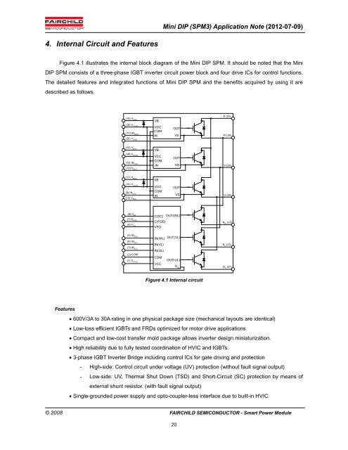
4. Internal Circuit and Features<br />
Mini DIP (SPM3) Application Note (2012-07-09)<br />
Figure 4.1 illustrates the internal block diagram of the Mini DIP SPM. It should be noted that the Mini<br />
DIP SPM consists of a three-phase IGBT inverter circuit power block and four drive ICs for control functions.<br />
The detailed features and integrated functions of Mini DIP SPM and the benefits acquired by using it are<br />
described as follows.<br />
Features<br />
(19) V B(W)<br />
(18) V CC(H)<br />
(17) IN (WH)<br />
(20) V S(W)<br />
(15) V B(V)<br />
(14) V CC(H)<br />
(13) IN (VH)<br />
(16) V S(V)<br />
(11) V B(U)<br />
(10) V CC(H)<br />
(9) IN (UH)<br />
(12) V S(U)<br />
(8) C SC<br />
(7) C FOD<br />
(6) V FO<br />
(5) IN (WL)<br />
(4) IN (VL)<br />
(3) IN (UL)<br />
(2) COM<br />
(1) VCC(L) VB<br />
VCC<br />
COM<br />
IN<br />
VB<br />
VCC<br />
COM<br />
IN<br />
VB<br />
VCC<br />
COM<br />
IN<br />
C(SC)<br />
C(FOD)<br />
VFO<br />
IN(WL) OUT(VL)<br />
IN(VL)<br />
IN(UL)<br />
COM<br />
VCC<br />
OUT(WL)<br />
OUT(UL)<br />
© 2008 FAIRCHILD SEMICONDUCTOR - Smart Power Module<br />
OUT<br />
20<br />
VS<br />
OUT<br />
VS<br />
OUT<br />
VS<br />
V SL<br />
Figure 4.1 Internal circuit<br />
600V/3A to 30A rating in one physical package size (mechanical layouts are identical)<br />
Low-loss efficient IGBTs and FRDs optimized for motor drive applications<br />
Compact and low-cost transfer mold package allows inverter design miniaturization.<br />
High reliability due to fully tested coordination of HVIC and IGBTs.<br />
3-phase IGBT Inverter Bridge including control ICs for gate driving and protection<br />
- High-side: Control circuit under voltage (UV) protection (without fault signal output)<br />
- Low-side: UV, Thermal Shut Down (TSD) and Short-Circuit (SC) protection by means of<br />
external shunt resistor. (with fault signal output)<br />
Single-grounded power supply and opto-coupler-less interface due to built-in HVIC<br />
P (27)<br />
W (26)<br />
V (25)<br />
U (24)<br />
N W (23)<br />
N V (22)<br />
N U (21)


