Topologically Defined Neuronal Networks Controlled by Silicon Chips
Topologically Defined Neuronal Networks Controlled by Silicon Chips
Topologically Defined Neuronal Networks Controlled by Silicon Chips

You also want an ePaper? Increase the reach of your titles
YUMPU automatically turns print PDFs into web optimized ePapers that Google loves.
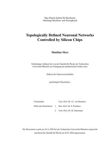
Max-Planck-Institut für Biochemie<br />
Abteilung Membran- und Neurophysik<br />
<strong>Topologically</strong> <strong>Defined</strong> <strong>Neuronal</strong> <strong>Networks</strong><br />
<strong>Controlled</strong> <strong>by</strong> <strong>Silicon</strong> <strong>Chips</strong><br />
Matthias Merz<br />
Vollständiger Abdruck der von der Fakultät für Physik der Technischen<br />
Universität München zur Erlangung des akademischen Grades eines<br />
Doktors der Naturwissenschaften<br />
genehmigten Dissertation.<br />
Vorsitzender: Univ.-Prof. Dr. J.L. van Hemmen<br />
Prüfer der Dissertation: 1. Hon.-Prof. Dr. P. Fromherz<br />
2. Univ.-Prof. Dr. M. Stutzmann<br />
Die Dissertation wurde am 24.11.2003 bei der Technischen Universität München eingereicht<br />
und durch die Fakultät für Physik am 26.01.2004 angenommen.
Summary<br />
Small neuronal networks with defined synaptic connection patterns could provide a unique tool for<br />
studying fundamental concepts in neuroscience, because they are much simpler than in vivo systems<br />
and give easy access to individual neurons. Field-effect transistors and capacitive stimulators implemented<br />
on a semiconductor chip establish a non-invasive neuron-silicon interface, that enables the long<br />
term supervision even of large neuronal assemblies.<br />
The present thesis addresses the experimental and technological aspects of network design. Based on<br />
existing transistor chips a new device was processed for the specific requirements here. Small chipcontrolled<br />
networks were grown from neurons of the snail Lymnaea stagnalis and characterized.<br />
First, a new method for directing neurite outgrowth was developed. It is based on topographic guidance<br />
cues consisting of pits and narrow connecting grooves, which were processed from SU-8 polyester photoresist.<br />
Neurons placed into the pits grew neurites that followed the grooves and established electrical<br />
synapses upon contact with other neurites or somata. These networks were studied with standard electrophysiology<br />
and the conductance of the synapses was determined. On average, it was larger than the<br />
conductance of synapses between cell pairs grown on protein tracks.<br />
Besides guiding their outgrowth, the topographic structures also keep neurites in the final geometry<br />
and confine cell bodies to the pits. This is a major advantage compared to techniques using chemical<br />
patterns; there, neurites and somata are frequently pulled away <strong>by</strong> forces exerted <strong>by</strong> the growth-cones.<br />
Moreover, the structures are reusable many times, which makes them very efficient.<br />
Building on established technologies for extracellular recording and stimulation of neural activity, a<br />
transistor chip was processed next. Its layout, 16 bidirectional contacts arranged in a 4x4 array, was<br />
especially designed for monitoring small, defined networks of snail neurons. Each contact comprised<br />
a buried channel field-effect transistor for recording action potentials, surrounded <strong>by</strong> capacitive stimulation<br />
spots. <strong>Chips</strong> were characterized electronically and tested with single neurons. The transistors<br />
recorded a variety of signal types, similar to the results of previous works. Most of the extracellular<br />
signals could be qualitatively explained with the point-contact model for the neuron-silicon interface<br />
and the Hodgkin-Huxley model describing the voltage dynamics of the neuron. Extracellular stimulation<br />
was very reliable, 5-10 square wave pulses with 1V-5V amplitude applied to the capacitive spots<br />
evoked action potentials in the cell above.<br />
The third step combined both technologies, SU-8 topographic structures and silicon chips. For the<br />
first time, hybrid networks with defined geometry were realized. The most fundamental system, the<br />
silicon-neuron-neuron-silicon loop, was studied in detail. Upon extracellular stimulation the respective<br />
presynaptic neuron fired an action potential, which was detected <strong>by</strong> the transistor. The signal propagated<br />
along the neurites, passed the synapse and depolarized the postsynaptic cell where it triggered<br />
an action potential, if the input was strong enough. Again, neuronal activity was recorded from the<br />
transistor underneath. Larger networks with three and four neurons were also grown and characterized.<br />
The examples presented here constitute proof-of-principle experiments. They demonstrate that topologically<br />
defined hybrid networks, combining biology and semiconductor technology, can be implemented<br />
in functional systems, and pave the way for future applications such as a ‘living’ neurocomputer.
Contents<br />
1 Introduction 1<br />
1.1 Why build topologically defined hybrid networks? . . . . . . . . . . . . . . . . . . . . 1<br />
1.2 <strong>Defined</strong> networks and extracellular recording, state-of-the-art . . . . . . . . . . . . . . 2<br />
1.3 Outline of this thesis . . . . . . . . . . . . . . . . . . . . . . . . . . . . . . . . . . . 3<br />
2 <strong>Networks</strong> of defined topography 5<br />
2.1 How to control neuronal outgrowth - an overview . . . . . . . . . . . . . . . . . . . . 5<br />
2.1.1 Axon guidance in vivo . . . . . . . . . . . . . . . . . . . . . . . . . . . . . . 5<br />
2.1.2 Chemical patterns . . . . . . . . . . . . . . . . . . . . . . . . . . . . . . . . . 6<br />
2.1.3 Substrate topography . . . . . . . . . . . . . . . . . . . . . . . . . . . . . . . 8<br />
2.1.4 Alternative techniques . . . . . . . . . . . . . . . . . . . . . . . . . . . . . . 9<br />
2.1.5 Which technique is best? . . . . . . . . . . . . . . . . . . . . . . . . . . . . . 9<br />
2.2 Cell Culture . . . . . . . . . . . . . . . . . . . . . . . . . . . . . . . . . . . . . . . . 10<br />
2.2.1 What neurons should be used? . . . . . . . . . . . . . . . . . . . . . . . . . . 10<br />
2.2.2 Culturing neurons from Lymnaea stagnalis . . . . . . . . . . . . . . . . . . . 12<br />
2.2.3 Cleaning of substrates . . . . . . . . . . . . . . . . . . . . . . . . . . . . . . 14<br />
2.3 Building defined networks - technological aspects . . . . . . . . . . . . . . . . . . . . 15<br />
2.3.1 Patterns of growth-promoting proteins . . . . . . . . . . . . . . . . . . . . . . 16<br />
2.3.2 Topographic structures . . . . . . . . . . . . . . . . . . . . . . . . . . . . . . 16<br />
2.4 Theory part I: Neurons, synapses and cables . . . . . . . . . . . . . . . . . . . . . . . 18<br />
2.4.1 Passive model and cable theory . . . . . . . . . . . . . . . . . . . . . . . . . 18<br />
2.4.2 Neural networks . . . . . . . . . . . . . . . . . . . . . . . . . . . . . . . . . 21<br />
2.4.3 Active model: Hodgkin-Huxley dynamics . . . . . . . . . . . . . . . . . . . . 26<br />
2.5 Results . . . . . . . . . . . . . . . . . . . . . . . . . . . . . . . . . . . . . . . . . . . 28<br />
2.5.1 Standard cell culture . . . . . . . . . . . . . . . . . . . . . . . . . . . . . . . 29<br />
2.5.2 Controlling neurite outgrowth . . . . . . . . . . . . . . . . . . . . . . . . . . 30<br />
2.5.3 Simple, defined networks . . . . . . . . . . . . . . . . . . . . . . . . . . . . . 33<br />
2.5.4 Characterization of synapses . . . . . . . . . . . . . . . . . . . . . . . . . . . 36<br />
2.5.5 Discussion . . . . . . . . . . . . . . . . . . . . . . . . . . . . . . . . . . . . 39<br />
3 Single neurons on chips 43<br />
3.1 Why extracellular recording with silicon chips? . . . . . . . . . . . . . . . . . . . . . 43<br />
3.2 Theory part II: Field-effect transistors . . . . . . . . . . . . . . . . . . . . . . . . . . 45<br />
3.2.1 The pn junction . . . . . . . . . . . . . . . . . . . . . . . . . . . . . . . . . . 45<br />
3.2.2 The inversion channel FET . . . . . . . . . . . . . . . . . . . . . . . . . . . . 46<br />
3.2.3 The buried channel FET . . . . . . . . . . . . . . . . . . . . . . . . . . . . . 47<br />
3.2.4 Noise mechanisms . . . . . . . . . . . . . . . . . . . . . . . . . . . . . . . . 49<br />
3.3 The transistor-stimulator chip . . . . . . . . . . . . . . . . . . . . . . . . . . . . . . . 50<br />
3.3.1 Design considerations and layout . . . . . . . . . . . . . . . . . . . . . . . . 51<br />
i
CONTENTS<br />
3.3.2 Processing . . . . . . . . . . . . . . . . . . . . . . . . . . . . . . . . . . . . 53<br />
3.3.3 Performance . . . . . . . . . . . . . . . . . . . . . . . . . . . . . . . . . . . 56<br />
3.3.4 Discussion . . . . . . . . . . . . . . . . . . . . . . . . . . . . . . . . . . . . 61<br />
3.4 Measurement setup . . . . . . . . . . . . . . . . . . . . . . . . . . . . . . . . . . . . 63<br />
3.4.1 Chip amplifier . . . . . . . . . . . . . . . . . . . . . . . . . . . . . . . . . . 63<br />
3.4.2 Hard and software . . . . . . . . . . . . . . . . . . . . . . . . . . . . . . . . 64<br />
3.4.3 Microscope and electrophysiology . . . . . . . . . . . . . . . . . . . . . . . . 65<br />
3.4.4 A typical experiment . . . . . . . . . . . . . . . . . . . . . . . . . . . . . . . 65<br />
3.5 Theory part III: Neuron-silicon interface . . . . . . . . . . . . . . . . . . . . . . . . . 67<br />
3.5.1 Models . . . . . . . . . . . . . . . . . . . . . . . . . . . . . . . . . . . . . . 67<br />
3.5.2 Capacitive stimulation . . . . . . . . . . . . . . . . . . . . . . . . . . . . . . 68<br />
3.5.3 Extracellular recording . . . . . . . . . . . . . . . . . . . . . . . . . . . . . . 70<br />
3.5.4 What do transistors measure? . . . . . . . . . . . . . . . . . . . . . . . . . . 72<br />
3.6 Neuron-silicon interface: Experimental results . . . . . . . . . . . . . . . . . . . . . . 73<br />
3.6.1 Capacitive Stimulation . . . . . . . . . . . . . . . . . . . . . . . . . . . . . . 73<br />
3.6.2 Extracellular recording: A gallery of signals . . . . . . . . . . . . . . . . . . . 74<br />
3.6.3 Bidirectional junction . . . . . . . . . . . . . . . . . . . . . . . . . . . . . . 76<br />
3.6.4 Dynamics of action potentials and transistor signals . . . . . . . . . . . . . . . 77<br />
3.6.5 Discussion . . . . . . . . . . . . . . . . . . . . . . . . . . . . . . . . . . . . 79<br />
4 <strong>Defined</strong> networks on chips 83<br />
4.1 Theory part IV: Chip-controlled networks . . . . . . . . . . . . . . . . . . . . . . . . 83<br />
4.2 Results . . . . . . . . . . . . . . . . . . . . . . . . . . . . . . . . . . . . . . . . . . . 84<br />
4.2.1 Basic silicon-neuron-neuron-silicon loop . . . . . . . . . . . . . . . . . . . . 84<br />
4.2.2 Partially controlled three-neuron network . . . . . . . . . . . . . . . . . . . . 87<br />
4.2.3 <strong>Defined</strong> network of four neurons . . . . . . . . . . . . . . . . . . . . . . . . . 89<br />
4.3 Final discussion . . . . . . . . . . . . . . . . . . . . . . . . . . . . . . . . . . . . . . 93<br />
4.3.1 Controlling neuronal activity from the chip . . . . . . . . . . . . . . . . . . . 93<br />
4.3.2 <strong>Defined</strong> networks in topographic structures . . . . . . . . . . . . . . . . . . . 94<br />
4.3.3 Stability of the chips . . . . . . . . . . . . . . . . . . . . . . . . . . . . . . . 94<br />
4.3.4 Yield, the decisive factor . . . . . . . . . . . . . . . . . . . . . . . . . . . . . 95<br />
4.3.5 Next steps . . . . . . . . . . . . . . . . . . . . . . . . . . . . . . . . . . . . . 96<br />
5 Conclusion and outlook 97<br />
A Cell culture protocols and recipes 99<br />
B Chip processing and characterization 102<br />
C Simulation of extracellular signals 106<br />
D Abbreviations 107<br />
Bibliography 109<br />
ii
Chapter 1<br />
Introduction<br />
This first chapter outlines the ideas and questions that led to the present thesis and briefly reviews<br />
relevant technologies. An overview of the contents of the other chapters concludes the introduction.<br />
1.1 Why build topologically defined hybrid networks?<br />
In vivo neural networks are highly complicated systems comprising up to 10 11 neurons with a complex<br />
pattern of synaptic connections. While recent advances in functional magnetic resonance imaging and<br />
positron emission tomography provide tools for monitoring the activity of whole brains, their temporal<br />
and spatial resolution is still far too low for studies at the single cell level.<br />
Despite these technological deficits, results from rather simple experiments, with impaled microelectrodes,<br />
inspired fundamental theoretical concepts like Hebbian learning or associative memory. Artificial<br />
systems have been developed, e.g. Hopfield networks, that resemble the natural ones to a smaller or<br />
larger extent. Such artificial systems can perform difficult tasks of information processing and are even<br />
used for commercial applications. However, most of them are implemented in special software running<br />
on ordinary computers and can therefore not profit from the massive parallel computing capabilities of<br />
the living neural networks they were adapted from. There are only a few examples where these ideas<br />
have been realized in hardware, namely custom made silicon chips. The high number of synaptic connections<br />
restricts network size on these chips to about 1000 neurons or less, even in the VLSI (very<br />
large scale integration; silicon processing technology) era [96].<br />
In consequence there is a large technological gap between theory on the one hand and the real world on<br />
the other. Eventually this gap could be bridged with a bottom up approach, the controlled assembly<br />
of well organized networks from living neurons in vitro. These networks would provide a unique tool<br />
for studying signal processing in biological nervous systems and their parallel computing capabilities<br />
could lay the foundations for novel computer systems.<br />
Nerve cell cultures are a common technique in neuroscience. They considerably reduce the number of<br />
neurons, compared to living brains and restrict the network to the 2D surface of the culture dish, there<strong>by</strong><br />
giving easy access to all neurons. Yet, synapses are still numerous and their connections remain unknown,<br />
obstructing any attempt to establish a theoretical model of the system.<br />
The problem could be overcome if it were possible to grow networks with defined synaptic connection<br />
pattern, e.g. the two layer perceptron in fig. 1.1.<br />
1
CHAPTER 1. INTRODUCTION<br />
Figure 1.1: Left: Piece of the human visual cortex with highly branched neurites and complex synaptic<br />
connection pattern, from [20]. Right: Schematic drawing of a simple, designed feed-forward network.<br />
Studying these systems, once they are established, requires long term control of network activity<br />
at the single cell level; action potentials must be evoked in and recorded from individual neurons.<br />
Standard electrophysiology, using impaled microelectrodes or patch clamp, is inappropriate because it<br />
harms the nerve cells, there<strong>by</strong> limiting the recording time to a few hours before cells die. Furthermore,<br />
spatial constraints with micromanipulators used for positioning the pipettes considerably restrict the<br />
number of cells that can be monitored. Alternative techniques are needed that are non-invasive, as<br />
sketched in fig. 1.2, and also can be scaled up to large neuronal assemblies .<br />
Figure 1.2: Invasive (left) and non-invasive (right) recording and stimulation of individual neurons.<br />
The aim of this thesis is to implement and study small networks of living neurons with a defined<br />
synaptic connection pattern. This requires advances in network design and extracellular recording,<br />
and lays the foundations for systematic tests of fundamental concepts in neuroscience.<br />
1.2 <strong>Defined</strong> networks and extracellular recording, state-of-the-art<br />
Since the ideas outlined above are not new, much work has already been done on network design and<br />
non-invasive recording. This paragraph gives a short overview of relevant technologies reported in the<br />
literature.<br />
A variety of methods exists for building topologically defined networks. Most of them use patterns<br />
of substrate-bound molecules that either promote or inhibit neurite outgrowth, e.g. silanes [56],<br />
poly-L-lysine [8] or proteins [81]. Neurons cultured on these substrates grow neurites that follow the<br />
permissive tracks while avoiding inhibitory areas. The patterns are made with techniques adapted from<br />
semiconductor processing, like photolithography [56], laser ablation [15] or microcontact printing [97].<br />
Although they guide advancing neurites rather well, somata and already grown neurites are frequently<br />
2
1.3. OUTLINE OF THIS THESIS<br />
displaced <strong>by</strong> pulling forces exerted <strong>by</strong> the growth-cones.<br />
In a preceding study [129], pillars processed from photoresist were used to mechanically immobilize<br />
the cell bodies on predefined sites.<br />
Much smaller topographic structures consisting of grooves or edges in the micrometer and nanometer<br />
range have been shown to affect neurite outgrowth, too [84]. Even though they have been proposed as<br />
a tool for designing networks, there are no reports about successful applications so far.<br />
Long term control of neuronal activity is only possible with techniques that contact neurons extracellularly.<br />
The simplest systems consist of metal spots processed onto planar substrates and connected<br />
to external amplifiers via insulated leads. Arrays of these electrodes, so-called MEAs (multi electrode<br />
arrays) are a common tool for monitoring network activity, for example in studies about the effects of<br />
chemicals on neuronal viability [76].<br />
In 1972, Bergveld [2] used field-effect transistors with non-metal gates to make recordings from muscle<br />
fibers of guinea pigs and in 1990 Fromherz et al. were able to detect action potentials from neurons<br />
of the leech Hirudo medicinalis with similar devices [33]. Since then, the neuron-silicon interface<br />
has been studied in detail and recordings were made from rat hippocampal neurons (only with signal<br />
averaging to reduce noise) and nerve cells from the snail Lymnaea stagnalis [50, 114, 129].<br />
1.3 Outline of this thesis<br />
Building chip-controlled networks raises several questions and problems that can be divided into three<br />
parts: choosing the appropriate neuronal cell culture, growing topologically defined networks of synaptically<br />
connected neurons, and bidirectional interfacing of neurons to silicon chips. In the course of the<br />
experimental work, these parts were first addressed separately, though sometimes in parallel, and then<br />
joined at the end. The thesis roughly follows this order.<br />
The next chapter covers all aspects of network design, from cell culture to theoretical concepts of signal<br />
propagation in neurites. After introducing the mechanisms governing axon guidance in vivo, methods<br />
for controlling neurite outgrowth in vitro are reviewed. The cell culture is then described, and the<br />
technological details of protein patterns and topographic structures are given, followed <strong>by</strong> a theoretical<br />
section on neurons and synapses. Finally, examples of defined neural networks are shown, characterized<br />
and discussed.<br />
Once these networks can be reliably grown, their activity should be controlled non-invasively, and this<br />
is the subject of chapter 3. It illustrates the theoretical and technological aspects of buried channel fieldeffect<br />
transistors and describes relevant processing steps. Fundamental principles of the neuron-silicon<br />
interface are given in a further theoretical section. At the end, experimental results on stimulation and<br />
recording via the chip are presented and discussed.<br />
Chapter 4 combines these techniques to establish chip-controlled, defined neural networks. After a<br />
brief recapitulation of theoretical concepts, three examples of increasing complexity are shown. The<br />
final discussion focuses on the efficiency of the single steps involved in growing the networks and the<br />
overall yield, and on how it may be increased.<br />
The final chapter 5 summarizes the results and provides an outlook towards future experiments and<br />
applications.<br />
Technological details of the cell culture and semiconductor processing, as well as parameters for simulations<br />
are outsourced to appendices.<br />
3
CHAPTER 1. INTRODUCTION<br />
4
Chapter 2<br />
<strong>Networks</strong> of defined topography<br />
The first section of this chapter summarizes the techniques for growth-cone guidance reported in the<br />
literature and discusses which best meet our experimental needs. Then the cell culture is introduced,<br />
followed <strong>by</strong> a detailed description of the methods used for guiding neurite outgrowth here, including<br />
relevant technological aspects. Basic theoretical concepts of neural networks like cable theory, synapses<br />
and the Hodgkin-Huxley model are introduced next. The chapter ends with a presentation of the results<br />
and their discussion.<br />
2.1 How to control neuronal outgrowth - an overview<br />
In the developing nervous system, axons must find the way to their target tissue over long distances.<br />
Many cues are involved in the process of pathfinding, which often act synergistically, thus increasing<br />
overall directional information. To elucidate the influence of individual cues on growing neuronal processes,<br />
many in vitro studies have been done. Their results are the basis for the engineering approach<br />
of growing defined neural networks.<br />
The cellular mechanisms, signaling pathways and molecules governing pathfinding are briefly introduced<br />
in the next subsection. Various techniques used for controlling neuronal outgrowth in vitro are<br />
presented thereafter, followed <strong>by</strong> a discussion of which are most appropriate for the applications here.<br />
2.1.1 Axon guidance in vivo<br />
The mature human nervous system consists of about 10 11 neurons with highly specific synaptic connections<br />
[53]. For example, axons emerging from the retina form an exact topographic representation<br />
of their origin at their target in the optic tectum.<br />
Guiding axonal outgrowth is the most important process in establishing these precise connection<br />
schemes. Axons grow and respond to environmental cues with specialized terminal protuberances<br />
called growth-cones. These are both sensory and motor structures that bear numerous receptors for directional<br />
cues as well as cytoskeletal proteins and actin based motors that propel them froward. Growthcones<br />
have three main domains: a central core which is rich in microtubules, mitochondria and many<br />
other organelles; the filopodia, thin extensions that project from the body; and lamellipodia, flat structures<br />
in between. Filopodia are highly mobile, rod-like actin-rich structures that scan their environment<br />
for directional cues. They are the major element of growth-cone sensory capability. Ligands binding to<br />
receptors in the filopodia membrane, e.g. extra cellular matrix protein (ECM) binding to integrin, stimulate<br />
the advance, retreat, or turn of growth-cones. The exact signaling pathways from ligand binding<br />
to directional movement are not yet fully understood [37], however, Ca 2+ plays an important role as a<br />
second messenger [39, 46].<br />
5
CHAPTER 2. NETWORKS OF DEFINED TOPOGRAPHY<br />
Figure 2.1: Four types of mechanisms contribute<br />
to guiding growth-cones: contact attraction,<br />
chemoattraction, contact repulsion<br />
and chemorepulsion. Individual growthcones<br />
might be ‘pushed’ from behind <strong>by</strong> a<br />
chemorepellant (red), ’pulled’ from afar <strong>by</strong> a<br />
chemoattractant (green), and ’hemmed’ in <strong>by</strong><br />
attractive (grey) and repulsive (yellow) local<br />
cues; from [110].<br />
Directional cues are either attractive or repulsive, long-range or short-range. The long-range guidance<br />
mechanism, called chemotaxis, is based on gradients of diffusible, soluble molecules, whereas the<br />
short-range contact-mediated mechanism is mediated <strong>by</strong> tissue-bound, non-diffusible molecules. Fig.<br />
2.1 depicts the four forces guiding growth-cones: contact attraction, chemoattraction, contact repulsion<br />
and chemorepulsion, and lists examples of ligands governing these mechanisms. Some guidance<br />
molecules are not exclusively attractive or repulsive but rather bifunctional, depending on their concentration,<br />
type of receptor and presence of other molecules. In vivo, neuronal outgrowth is generally<br />
controlled <strong>by</strong> several cues acting simultaneously and synergistically, e.g. the growth-cone is repelled<br />
from its origin <strong>by</strong> one ligand and attracted to the target tissue <strong>by</strong> another.<br />
Besides these ligand-mediated cues, axonal outgrowth is further influenced <strong>by</strong> trophic factors that are<br />
needed for survival and growth as well as <strong>by</strong> adhesion molecules providing adhesive surfaces for the<br />
growth-cone.<br />
Although many directional signals are present in vivo, in vitro studies revealed that a single ligand is<br />
often sufficient for controlling neuronal outgrowth. These studies set the stage for the design of defined<br />
neuronal nets.<br />
2.1.2 Chemical patterns<br />
Tracks of substrate bound molecules that are either attractive or repulsive to growth-cones (haptotaxis)<br />
are the most widely used technique for growth-cone guidance in vitro. In contrast to gradients of soluble<br />
molecules, they are easy to produce and can be kept in culture medium for a week or more without<br />
loosing their potency.<br />
Two major issues are raised with chemical patterns: what molecules are best and how to deposit them<br />
on the substrate? The vast body of literature on this subject is summarized <strong>by</strong> several comprehensive<br />
reviews [5, 22, 30, 52, 54].<br />
In an early experiment, P.C. Letourneau deposited areas of palladium onto different substrates <strong>by</strong> evaporation<br />
through EM-grids as masks [61]. Growth-cones from chick sensory ganglia neurons preferentially<br />
elongated on the more adhesive areas; for Pd on glass petri dishes they stayed on the Pd, while if<br />
polyornithine-coated dishes were used they preferred the Pd-free areas.<br />
Since then, many chemicals have been tested for patterns controlling cell adhesion and neuronal outgrowth.<br />
Among them are adhesive proteins like extracellular matrix protein (ECM) [35], laminin [42],<br />
growth factors [81] and nonadhesive proteins like albumin [21]. Artificial growth-promoting molecules<br />
such as poly-L-lysine and poly-D-lysine [8], and inhibitors such as poly ethylene glycol (PEG) are also<br />
common [121]. All these substances are only physisorbed to the substrate. Due to the weak binding<br />
6
2.1. HOW TO CONTROL NEURONAL OUTGROWTH - AN OVERVIEW<br />
Figure 2.2: Techniques for patterning chemicals onto surfaces. A, B: Photolithography with selective<br />
deposition (A) or removal (B) of molecules. C: Resist free lithography. D: Microcontact printing. E:<br />
Microfluidic networks.<br />
forces involved, this may result in gradual desorption and release to the cell culture medium with a subsequent<br />
loss of directional information. Conversely, self-assembled monolayers of silanes and thiols are<br />
tightly bound to silicon or gold surfaces <strong>by</strong> covalent bonds, making them very resistant to desorption.<br />
Silane patterns on Si-wafers have been cleaned and reused in hippocampal cell culture several times<br />
without loosing their directional information [23]. Above all, their adhesive properties can be tailored<br />
<strong>by</strong> appropriate terminal groups. Fluorinated, chlorinated and alkyl chains [56, 87, 100] inhibit protein<br />
binding and neuronal outgrowth, while amino groups promote it [87]. Complex molecules that are not<br />
compatible with silane or thiol chemistry, like proteins and peptides, can be covalently bound to substrates<br />
<strong>by</strong> heterobifunctional crosslinkers [8, 95, 121].<br />
Molecules are patterned onto the substrate with techniques adapted from microelectronic device fabrication.<br />
These are summarized in fig. 2.2.<br />
D. Kleinfeld et al. were the first to use photolithography for producing pathways of adhesive and nonadhesive<br />
silanes [56]. Their technique has been adapted <strong>by</strong> many researchers since then [16, 126].<br />
Photoresist is spin-coated on a substrate, usually a silicon wafer, silica or glass, exposed through a<br />
lithographic mask, and developed. The substrate is then incubated with a solution containing growth<br />
mediating molecules; the molecules bind to the resist as well as to uncovered areas. Stripping the resist<br />
leaves patterns of guidance molecules surrounded <strong>by</strong> areas of blank substrate, see fig. 2.2A.<br />
In fig. 2.2B, a similar technique is illustrated, with the main difference being that surface-bound<br />
molecules are selectively removed rather than deposited [16]. Before spinning photoresist, the substrate<br />
is uniformly coated with the desired molecules. Again, substrates are exposed and the resist is<br />
developed. A plasma etch removes guidance molecules in regions not protected <strong>by</strong> the resist, leaving a<br />
pattern complementary to the one in fig.2.2A after resist stripping.<br />
Photolithography is an excellent tool for functionalizing surfaces with down to sub-micrometer resolution<br />
in any desired geometry. However, the harsh solvents (e.g. acetone) involved in the lithographic<br />
process are not compatible with many guidance molecules such as proteins. This problem is overcome<br />
<strong>by</strong> recently developed techniques illustrated in fig.2.2C-E.<br />
Photoresist and solvents are completely omitted if UV light is used directly to selectively destroy, ablate<br />
or photocleave a homogeneous layer of growth mediating molecules. Washing away the residues in the<br />
exposed areas leaves intact chemicals in the areas shielded from the UV light <strong>by</strong> the mask. The only<br />
requirement here is UV light with a wavelength short enough to destroy or photocleave molecules, or<br />
with sufficient power for ablation (e.g. ArF laser λ=193nm). Several chemicals have been patterned<br />
7
CHAPTER 2. NETWORKS OF DEFINED TOPOGRAPHY<br />
with this technique, ranging from the denaturation of laminin [42], growth factors [81], ECM [35] and<br />
ablation of poly-L-lysine [15, 87] to the photocleavage of covalently bound organosilane monolayers<br />
[24].<br />
Conversely, UV light can also be used to selectively bind molecules in exposed areas to the substrate<br />
<strong>by</strong> special photoreactive cross-linkers [5].<br />
Softlithography is the general term for a number of methods that use soft devices (usually consisting<br />
of PDMS, polydimethylsiloxane, Sylgard 184, Dow-Corning) to stamp or generate chemical tracks <strong>by</strong><br />
capillary flow. They are made <strong>by</strong> curing a prepolymer on a photoresist master or structures etched into<br />
a Si-wafer.<br />
Stamps wetted with ‘ink’ (guidance molecules) are gently pressed onto the substrate. Molecules attach<br />
to the surface and reproduce the raised areas of the stamp. G.M. Whitesides was the first to use microcontact<br />
printing for covalently linking thiol patterns to gold surfaces [97].<br />
Microfluidic networks consist of PDMS membranes with relief structures that seal tightly against planar<br />
surfaces, forming micro-conduits [21]. Solutions are driven into the network of channels <strong>by</strong> capillary<br />
forces or application of pressure. Molecules adhere to the channel walls, one of which being<br />
the substrate. Removing the PDMS device leaves a pattern identical to the conduits on the surface,<br />
see Fig.2.2E. Complex structures with lanes of different molecules can be produced in a single step <strong>by</strong><br />
multiple laminar fluid flow in capillary networks [11, 109].<br />
Softlithography is an easy to use, inexpensive technique for producing complex patterns of surfacebound<br />
molecules. Except for master fabrication, no cleanroom equipment is required. Resolution is<br />
slightly reduced as compared to photolithography, but feature sizes down to 2µm are more than sufficient<br />
for most biological applications. For more information refer to the comprehensive reviews <strong>by</strong><br />
G.M. Whitesides et al. [54, 127]<br />
So far, all protocols resulted in chemical patterns surrounded <strong>by</strong> blank substrate. To increase directional<br />
information these areas are often coated with molecules bearing the complementary signal [56],<br />
e.g growth-promoting tracks surrounded <strong>by</strong> inhibitory regions. This is simply done <strong>by</strong> incubating the<br />
respective molecules on the prepatterned substrates as they only bind to the blank but not to the functionalized<br />
areas. The synergistic action of both cues increases directional information on growth-cones.<br />
This is especially important to prevent non-specific binding of serum (sometimes used with the culture<br />
medium) or proteins released <strong>by</strong> cells to the surface, which otherwise reduce the potency of the initial<br />
cues.<br />
2.1.3 Substrate topography<br />
In vivo, topographic features of the surrounding tissue provide morphogenetic guidance cues to growthcones.<br />
For example, growing axons fasciculate with pioneer axons, follow them for a certain distance,<br />
and defasciculate again. During fasciculated outgrowth, the growth-cone of the elongating axon is in<br />
physical contact with the pioneer axon and follows its topographic information.<br />
In vitro experiments are an elegant way to study the so far poorly understood signal transduction pathways<br />
involved in contact-mediated guidance and the role of the cytoskeleton [84]. Chemical cues<br />
abundant in in vivo systems can be completely excluded, leaving topographic structures as the only<br />
environmental information. A multitude of cells such as neurons, astroglial cells, MDCK, epithelial<br />
cells and many more were explanted onto glass, polymer and silicon substrates with rough surfaces or<br />
regular structures such as steps and grooves, with feature sizes ranging from nanometers to micrometers;<br />
see reviews <strong>by</strong> [4, 18, 19, 22, 29, 52].<br />
For example, astroglial cells preferentially grow on top of a regular array of columns with 0.5µm diameter<br />
etched into silicon, while avoiding irregular nanometer-sized surface roughness [17]. BHK cells and<br />
8
2.1. HOW TO CONTROL NEURONAL OUTGROWTH - AN OVERVIEW<br />
chicken neurons align and extend processes along simple step cues of sufficient height (1µm-10µm)<br />
processed into perspex [12] and orient in parallel to multiple grooved substrates [13]. Hippocampal<br />
neurons grow in parallel to deep, wide grooves but perpendicular to shallow narrow grooves [73, 83].<br />
Some studies examined the synergistic and hierarchic effects of chemical and topographic cues simultaneously<br />
presented to BHK cells [9], while others tested the behavior of cells embedded into an artificial<br />
three-dimensional structure [63].<br />
Most experiments done in this area of research so far were focused on studying the general features<br />
of cell-substrate interaction and how they relate to in vivo systems. Up to now, there were only few<br />
attempts to use topographic information for growing defined neural networks [22, 51].<br />
2.1.4 Alternative techniques<br />
Growth-cones of vertebrate and invertebrate neurons turn towards the cathode of a weak DC electric<br />
field applied to the culture medium [23, 69].<br />
This electric field guided neuronal outgrowth is called galvanotropism. It is based on the rearrangement<br />
of charged membrane proteins and receptors that are subject to an electrophoretic force. However, as<br />
most of these molecules bear negative excess charges outside the cell membrane, they should accumulate<br />
in the direction of the anode and promote growth towards it, away from the cathode. Electroosmotic<br />
effects might account for this contradictory behavior. Positively charged molecules surrounding<br />
the membrane (diffuse double layer) are driven towards the cathode, generating a flux of medium in<br />
this direction. The net force on the membrane proteins results from the superposition of the shear force<br />
created <strong>by</strong> the electroosmotic flux, and the electrophoretic force on the charged proteins themselves.<br />
Theoretical considerations and experiments have shown that, depending on membrane and protein parameters,<br />
this may result in proteins being pulled towards the anode or the cathode [70].<br />
Furthermore, the electric field depolarizes the membrane facing the cathode opening voltage-dependent<br />
Na + and Ca 2+ channels. Although the signalling cascades are not completely understood, Ca 2+<br />
seems to play an important role in controlling neuronal outgrowth, with the growth-cone moving towards<br />
higher internal Ca 2+ concentrations [69]. Thus, the influx of Ca 2+ makes the neurite grow<br />
towards the cathode.<br />
Only recently, light was successfully used to guide growing neurites [27]. Unlike the established technique<br />
of optical tweezers, the laser power was too low to hold or move growth-cones. Instead, the light<br />
may influence biological processes <strong>by</strong> mediating the actin polymerization-driven extension of lamellipodia<br />
through weak gradient forces generated <strong>by</strong> the laser beam.<br />
Pulsed magnetic fields have been shown to influence neuronal outgrowth [64], too. Dorsal root ganglia<br />
exposed to these fields exhibit asymmetric growth and an enhancement of neurite length. Unfortunately,<br />
the effect is not very controllable so far.<br />
2.1.5 Which technique is best?<br />
Out of the various techniques presented above, only a few are optimized sufficiently to reliably guide<br />
growing neurites. Even fewer fulfill the requirements arising from the combination with transistor chips<br />
for extracellular recording, listed in subsection 2.5.5.<br />
In their present developmental stage, DC electric fields, light and pulsed magnetic fields are not suitable.<br />
Either guidance is too weak, as with light and magnetic fields, or it is very difficult, if not impossible,<br />
to control the growth of several neurites simultaneously, as in the case of constant electric fields applied<br />
with pipettes. However, light, electric and magnetic fields can be turned on and off whenever needed.<br />
This inherent flexibility makes them first choice for directing growth-cones to the left or to the right on<br />
9
CHAPTER 2. NETWORKS OF DEFINED TOPOGRAPHY<br />
Figure 2.3: Leech neuron growing on tracks of intact ECM proteins (bright grey) surrounded <strong>by</strong><br />
regions of inactivated ECM. A: After 44h. B: After 68h. Pictures from [35].<br />
an intersection of chemical tracks [23].<br />
Patterns of substrate bound molecules represent the most developed technique for controlling neuronal<br />
outgrowth in vitro. They reliably guide growing neurites and can be aligned to any flat structures, e.g.<br />
micro-electrode arrays. Most molecules conveying directional information are compatible with extracellular<br />
recording. Moreover, pathways made from silane have been reused several times in culture<br />
before losing their directive properties, which makes them very efficient with respect to labor and cost<br />
[23]. The major drawback with this technique is that the molecules frequently do not provide enough<br />
force to keep the network in the grown geometry. Fig. 2.3 shows how neurites initially grown on tracks<br />
of extracellular matrix proteins (ECM) get pulled off <strong>by</strong> forces generated <strong>by</strong> the advancing growthcones.<br />
This problem is even more severe when somata are pulled away from electrodes or transistors<br />
as this makes extracellular recording impossible [50].<br />
Topographic structures are promising since they confine cells and neurites to the desired areas on the<br />
substrate <strong>by</strong> mechanical forces strong enough to prevent any dislocation. For example, pillars arranged<br />
in a circle around FETs reliably retained somata on the gates [130]. Moreover, substratum topography<br />
can also control neurite outgrowth, as shown <strong>by</strong> many studies culturing neurons on groove ridge structures,<br />
see 2.1.3. Although not confirmed experimentally, there is no obvious reason why this technique<br />
might interfere with extracellular recording.<br />
With the two latter approaches having their pros and cons, we decided to follow them both in the initial<br />
phase of the thesis: chemical patterns made from adsorbed growth-promoting factors and substrates<br />
with topographic structures.<br />
2.2 Cell Culture<br />
Choosing the right type of neurons and appropriate cell culture conditions is crucial for establishing<br />
chip-controlled neural networks. After a discussion of these issues, the isolation procedure for neurons<br />
and various cell culture methods are described. The section ends with an overview of the cleaning<br />
procedures applied to different types of substrates.<br />
2.2.1 What neurons should be used?<br />
As shown in section 2.1, many different types of neurons can be used for growing topologically defined<br />
networks. However, the combination with extracellular recording <strong>by</strong> FETs reduces the options considerably.<br />
Furthermore, not every neuron couples to the chip underneath (see 3.6.5 for details), making<br />
additional measurements with conventional microelectrodes necessary. This limits the number of cells<br />
that can be monitored at the same time to just a few. From these considerations the following criteria<br />
are deduced:<br />
10
2.2. CELL CULTURE<br />
Figure 2.4: A: Pond snail Lymnaea stagnalis on a Si-wafer. B: Schematic drawing of the dorsal view<br />
of the snail during preparation. n = needle, t = tentacle, p = penis, bw = body wall, ma = mantle,<br />
vm = visceral mass (deshelled), vo = visceral organs (pinned aside), es = esophagus, cgr = central<br />
ganglionic ring, cc = cerebral commissure, f = foot, bm = buccal mass, e = eye, mo = mouth; from [79].<br />
– large soma diameter to enable identification, isolation and positioning of individual cells<br />
– reliable stimulation and recording of single action potentials with silicon chips<br />
– formation of peripheral synapses<br />
– strong synaptic connections with inputs from some or even just one neuron triggering post-synaptic<br />
action potentials<br />
– small networks of only a few neurons should perform simple tasks of information processing<br />
Although vertebrate neurons, e.g. rat hippocampal neurons, are frequently cultured on multielectrode<br />
arrays [40] and are used to build networks of defined geometry in vitro [95], they are not ideal for our<br />
experiments. Soma diameters in the range of just 10µm make the isolation and positioning of individual<br />
cells very difficult. Also, small neurons give rise to only small electrical signals, resulting in<br />
bad signal-to-noise ratios. So far, recording action potentials from individual rat hippocampal neurons<br />
with field-effect transistors was only possible when signals were averaged to reduce noise [114, 115].<br />
In addition, functional neuronal units in vertebrates are generally rather complex, with single neurons<br />
receiving about 10 3 synaptic inputs. This makes the in vitro reconstruction of the functional units impossible.<br />
These problems put the focus on invertebrates, particularly molluscs. Their large (sometimes more<br />
than 100µm in diameter) and robust cell bodies facilitate the isolation and positioning of neurons and<br />
give rise to acceptable signal-to-noise ratios. The first neuron-silicon coupling has been achieved with<br />
neurons from the leech Hirudo medicinalis [33] and many experiments have been done since [112].<br />
Leech neurons also grow processes along predefined pathways of ECM proteins and seem to form neural<br />
networks. Despite these promising features, leech neurons are not used here because only very weak<br />
peripheral synapses are established in vitro, and at an extremely low yield [38, 93].<br />
Lymnaea stagnalis is a freshwater snail that can be found in ponds all across Europe; fig. 2.4A shows a<br />
picture of the species. Its neurons have soma diameters up to 100µm and are known to form synaptic<br />
11
CHAPTER 2. NETWORKS OF DEFINED TOPOGRAPHY<br />
connections in vitro [65, 66, 106]. Small networks of only a few neurons perform tasks such as generating<br />
the rhythm for feeding and breathing. Due to their simplicity, these networks are ideal for studying<br />
principles of information processing at a single cell level. N.I. Syed et al. were able to reconstruct the<br />
central pattern generator that controls the animal’s breathing rhythm, from dissociated neurons in vitro<br />
[105]. However, these identified neurons, R.Pe.D1, V.D4 and Ip.3.1, are difficult to isolate. Generally,<br />
the number of cells forming chemical synapses in culture is very small.<br />
The A-clusters of the two paired pedal ganglia comprise about 60 cells with similar electrophysiological<br />
properties [98] and electrical synapses between them [58]. Due to the large number and diameters<br />
ranging from 40µm-70µm, A-cluster neurons are ideal for designing artificial neural networks in vitro.<br />
A more pragmatic reason for choosing Lymnaea stagnalis and not Aplysia californica, an even better<br />
analyzed mollusk with equally promising neural properties, as a neuron donor is Lymnaea’s simple<br />
and robust nature and its availability. The snails are kept in four 200L basins that are cleaned twice<br />
a week. They are fed on lettuce and fish food pellets. To prevent inbreeding or population decreases<br />
due to reproduction rates not matching the number of animals needed, new snails are added at irregular<br />
intervals. A quarantine basin prevents the contamination of the laboratory stock with parasites.<br />
2.2.2 Culturing neurons from Lymnaea stagnalis<br />
The isolation and culture of Lymnaea neurons follows protocols from the literature [90, 107], with<br />
minor modifications. For a detailed, well illustrated description see [49].<br />
All steps, except the removal of the shell, are executed under sterile conditions in a flowhood. Dissection<br />
instruments are either autoclaved or soaked in a solution of 70% ethanol and 30% water prior to the<br />
preparation. The entire procedure is divided into two parts, the isolation of individual neurons including<br />
their positioning on the chip, and the subsequent cell culture to enable neuronal outgrowth and synapse<br />
formation. While the general aspects are outlined below, details of single steps and recipes for solutions<br />
and culture media are described in appendix A.<br />
Isolation of individual cells<br />
Animals with a shell length of 1.5cm-2cm are selected from the laboratory stock and deshelled. They<br />
are soaked in antibacterial solution for 5min to remove dirt and bacteria and to anaesthetize them. They<br />
are then pinned to a culture dish with a rubber coating at its bottom which is filled with antibiotic normal<br />
saline (ABS). An incision is made on the dorsal surface from the mouth to the visceral mass. The body<br />
wall and internal organs are pinned aside to expose the brain, consisting of a loop of ganglions located<br />
at the end of the buccal mass, see fig. 2.4B for a sketch of the snail at this stage of the preparation. Next,<br />
the cerebral commissure and the esophagus are cut with fine scissors and the buccal mass is removed.<br />
After cutting the remaining nerves connecting the ganglia to the body, the central ganglionic ring is<br />
transferred to a small dissection dish also filled with saline.<br />
To extract individual neurons, the brains are pinned to the rubber coated dish and the outer sheath,<br />
the connective tissue surrounding the ganglia, is carefully removed with fine tweezers. The saline is<br />
exchanged to remove debris and tissue parts. Central ganglionic rings now look like the one shown in<br />
fig. 2.5A. After 15min, during which the brains recover from the previous step, they are treated with an<br />
enzyme solution for 27min-33min. The enzymes partly digest the extracellular matrix, thus facilitating<br />
the isolation of individual neurons from the ganglia. The brains are then washed three times with defined<br />
medium to remove the enzymes and are incubated in trypsin inhibitor for 15min, which inactivates<br />
any trypsin remaining in spite of the previous washes. Following three more washes, the medium is<br />
replaced with high osmolarity defined medium. The increased osmolarity causes a slight shrinkage of<br />
the neurons that makes the somata less susceptible to mechanical damage and facilitates their isolation.<br />
The inner connective tissue sheath surrounding each ganglion is opened with a microneedle, and indi-<br />
12
2.2. CELL CULTURE<br />
Figure 2.5: A: Dorsal view of a central ganglionic ring pinned to a dissection dish after removal of the<br />
outer sheath. B: Schematic drawing with the A-clusters of the left and right pedal ganglion marked in<br />
red. The neurons forming the central pattern generator for respiration are also highlighted.<br />
vidual neurons are removed with a glass micropipette <strong>by</strong> aspiration. To check the vitality, neurons are<br />
gently flushed out of the pipette and optically inspected after settling to the bottom of the dish. Healthy<br />
cells have a pearly shine and an intact cell membrane. Only these are transferred to the prepared culture<br />
chamber and placed in the pits on the substrate. Culture chambers are incubated at 20 ◦ C in a humid environment<br />
to prevent evaporative loss of medium. <strong>Neuronal</strong> outgrowth begins a few hours after plating<br />
the cells and lasts for several days.<br />
About 10-15 vital neurons can be extracted from the A-cluster regions of the paired pedal ganglia.<br />
Therefore, 6 to 8 brains are usually processed in parallel to provide enough cells for up to six transistor<br />
chips to be prepared at the same time.<br />
Cell culture methods<br />
While Lymnaea neurons can survive for several days in plain defined medium, neurotrophic factors<br />
are needed to promote the outgrowth of neurites [125]. These presumably proteinaceous substances<br />
are released from snail brains directly into the defined medium in which they are incubated. Although<br />
nerve growth factor has a similar effect on some types of brain cells, the composition of the secreted<br />
substances is more complex and not yet known [90].<br />
There are several ways to deliver these factors, which are essential for the growth of neural networks<br />
in vitro, to the neurons in the culture dish. They all depend on brains for growth factor production.<br />
Central ganglionic rings are isolated from animals with a shell length of about 3cm, following the first<br />
part of the procedure outlined above. They are transferred to Falcon 3001 culture dishes and incubated<br />
for roughly two hours in antibiotic saline that is exchanged five times during this period. After this<br />
treatment the tissue is sterile and ready to be used in one of the methods described below:<br />
Conditioned medium (CM): A convenient and common way to deliver growth factors to neurons is the<br />
use of brain conditioned medium [66, 107]. Central ganglionic rings are incubated in defined medium<br />
at a concentration of 2brains/ml in a humid environment. A glass culture dish coated with Sigmacote<br />
SL2 (Sigma) is used to reduce loss of proteins. After 72h the supernatant is filtered through a low<br />
protein binding syringe filter, shock frozen in cryovials and stored at -20 ◦ C in the freezer. The CM is<br />
thawed prior to use and filled into the culture chambers.<br />
However, this elegant method did not produce satisfactory results, neuronal outgrowth was poor. Possible<br />
reasons might be excessive protein loss during numerous media transfers due to proteins adhering<br />
to the surfaces of the syringe, vials etc., or unknown contamination of the CM.<br />
13
CHAPTER 2. NETWORKS OF DEFINED TOPOGRAPHY<br />
Substrate adsorbed material (SAM): This method is based on the adhesive properties of the trophic<br />
factors that adhere very well to poly-L-lysine coated substrates, forming a robust layer of growthpromoting<br />
proteins [79, 124]. Lymnaea brains are incubated directly in the culture chamber at 2brains/ml<br />
medium for 72h. Before plating the neurons, the brains are removed and the supernatant is either diluted<br />
1:1 or completely replaced <strong>by</strong> defined medium. The growth factors attached to the bottom of the<br />
chamber are sufficient to promote vigorous neurite outgrowth.<br />
Layers of SAM are also used to grow topologically defined networks with a technique described in<br />
2.3.1. However, SAM is incompatible with extracellular recording <strong>by</strong> transistors. The adsorbed proteins<br />
form a cushion on the chip surface, there<strong>by</strong> increasing the distance between transistor and neuron,<br />
obstructing a successful neuron-silicon coupling.<br />
Co-culture: The drawbacks of the aforementioned methods can be avoided if neurons and brains are<br />
cultured together, with the ganglionic rings added after the neurons are plated. This allows the neurons<br />
to adhere tightly to the uncovered sticky poly-L-lysine coated surface of the substrate, while the growth<br />
factors are delivered directly to the medium without any loss. As no proteins are present at the time<br />
neurons are placed and secretion starts only after brains are added to the medium, neuronal outgrowth<br />
is delayed for about one day compared to the other methods. The overall success of the co-culture is<br />
not affected <strong>by</strong> this.<br />
2.2.3 Cleaning of substrates<br />
Before neurons were plated, the substrates had to be cleaned, sterilized and coated with poly-L-lysine.<br />
The two latter steps, being rather simple, are described in appendix A, whereas cleaning is discussed<br />
here since it turned out to be problematic. It must be aggressive enough to reliably remove tissue and<br />
debris from previous cell cultures, yet mild enough so as not to affect the substrates. As substrates became<br />
more sophisticated, the demands on the cleaning procedure increased as revealed <strong>by</strong> the following<br />
list:<br />
Glass coverslips: Round cover glasses (diameter 30mm, thickness 1, Assistent) were treated with<br />
acidic and alkaline detergent in an ultrasonic cleaner at 80 ◦ C according to a procedure adapted from<br />
[34] (for details see appendix A). The coverslips were only used once.<br />
Substrates with topographic structures: Topographic structures consist of polyimide or SU-8 polyester<br />
photoresist processed onto glass coverslips and oxidized silicon wafers, see subsection 2.3.2. Due<br />
to internal stress and a different thermal expansion coefficient than the underlying substrate, the resist<br />
layers peel off upon prolonged sonication and temperature shocks. To meet these new requirements,<br />
the previously described procedure was modified. While the time the substrates were immersed in the<br />
detergents was not altered, the temperature was reduced to 50 ◦ C and the overall sonication time was<br />
limited to 5min. Preheated water was used for rinsing to avoid thermal shock. The method allowed<br />
substrates to be recycled five times before the resist began to peel off, but was efficient enough to reliably<br />
remove tissue and dirt in the pits and grooves of the topographic structures.<br />
Transistor chips: Transistor chips are rather complex devices with many different materials (SiO2,<br />
polyester resist, silicone adhesive and PMMA) exposed to the cell culture and thus to subsequent cleaning.<br />
For a detailed description of the chips refer to subsection 3.3.2 and fig. 3.6.<br />
Without the topographic structures, removal of tissue and debris would be easy; mild detergent and<br />
Q-tips for a slight scrubbing are sufficient for conventional chips [49]. However, feature sizes down<br />
to 14µm render the mechanical cleaning of the chips here difficult. There are no brushes with bristles<br />
that fit in the narrow grooves. Methods solely based on chemical treatment are problematic though,<br />
because they either are too aggressive to the device or the results are not satisfactory, with impurities<br />
14
2.3. BUILDING DEFINED NETWORKS - TECHNOLOGICAL ASPECTS<br />
remaining in the structures. The following list shows various procedures tested throughout this study.<br />
All chips were precleaned with Q-tips and a pressurized water jet to mechanically remove as much<br />
tissue as possible.<br />
– The alkaline detergent of the process described above has pH14. It etches the gate oxide at a<br />
considerable rate (0,5 ˚A/min at 80 ◦ C [59]), leading to a quick failure of the transistors if devices are<br />
exposed to the solution for extended times. To minimize negative effects on the gate oxides, the<br />
liquid was applied for only 2 minutes and sonication was omitted completely to prevent damaging<br />
the structures. The cost of these modifications were modest results with tenacious dirt remaining<br />
in the grooves.<br />
– A lukewarm solution of dishwasher detergent proved very efficient. Organic material was dissolved<br />
within minutes, leaving a clean surface even within the structures. The gate oxide does not deteriorate<br />
because the solution has a rather mild pH11. Moreover the detergent was applied for only<br />
5min. Despite these promising features, neuronal outgrowth was poor on chips subjected to this<br />
procedure and many neurons died.<br />
– Treatment with the enzymes collagenase dispase and trypsin or with contact lens cleaner was not<br />
satisfactory; not all cell rests were removed.<br />
– In [129] a hot, very reactive mixture of 2:1v/v H2SO4 and H2O2, called piranha solution was used<br />
on chips with polyimide columns. Due to their larger surface and different material properties,<br />
the topographic structures here are much more susceptible to thermal shock than the columns. To<br />
prevent SU-8 resist from peeling off, only cold solution could be used. The decreased activity was<br />
compensated <strong>by</strong> increasing the residence time to 90s. Unlike the procedure described in [129],<br />
only small drops of piranha solution were applied to the center of the chip with conventional plastic<br />
pipettes. Any contact between drops and culture chamber had to be avoided, since the acid<br />
dissolved the silicone adhesive, leaving a whitish scum on the chip. If executed correctly the chips<br />
were clean after the procedure and could be reused many times.<br />
– Instead of piranha solution, chromosulfuric acid was applied for 3 x 15s following the same protocol.<br />
Results were very good, as no tissue remained on the chip. Except for minor damage to the<br />
PMMA chamber if it came in contact with the liquid, the device was not affected at all. However,<br />
the analysis of I-V curves revealed a strong effect of the Cr ions on the transistor characteristics,<br />
see 3.3.3. Since chromosulfuric acid is very toxic, a thorough rinsing was mandatory afterwards.<br />
– Ordinary dishwashing liquid assisted <strong>by</strong> mechanical scrubbing with a brush is a mild way for<br />
removing dirt. While the chamber walls and even the pits of the topographic structures got perfectly<br />
clean, some tissue remained in the grooves because they were not accessible to the brush.<br />
After cleaning, no matter which protocol was used, the chips were washed several times with the pressurized<br />
water jet to remove detergent and rinsed frequently during at least 3h. Milli-Q water (Millipore)<br />
was used throughout all steps.<br />
Except for the dishwasher detergent, all protocols provided chips that did not harm cells and enabled<br />
neuronal outgrowth. Due to the varying success of cell culture, many different procedures were tested.<br />
At the moment, none of them allows reliable results. Sometimes many neurons were vital and grew processes<br />
that followed the grooves, sometimes survival and growth was poor. Whether this can be solely<br />
ascribed to the cleaning protocol, or if other factors are involved remains unclear; see the discussion in<br />
2.5.5.<br />
2.3 Building defined networks - technological aspects<br />
Initially, two techniques were tested for growing defined networks with snail neurons, one based on<br />
chemical patterns, the other on surface topography. Their technological aspects are presented in the<br />
following paragraphs, detailed parameters for SU-8 processing are listed in appendix B.<br />
15
CHAPTER 2. NETWORKS OF DEFINED TOPOGRAPHY<br />
Figure 2.6: Schematic illustration of the patterning procedure.<br />
2.3.1 Patterns of growth-promoting proteins<br />
Tracks of intact extracellular matrix proteins (ECM) surrounded <strong>by</strong> UV-inactivated areas have shown<br />
to reliably guide growing leech neurites [35]. This technique has been adapted to the requirements of<br />
Lymnaea neuronal cell culture <strong>by</strong> A. Prinz [79]. Instead of ECM, substrate-adsorbed material (SAM)<br />
is patterned with UV light. The procedure involves the following steps, which are also illustrated in fig.<br />
2.6:<br />
– deposit a layer of SAM on glass coverslips as described in section 2.2.2<br />
– remove conditioning brains, supernatant and flexiPERM adhesive culture chambers (in vitro Systems<br />
& Services, Osterode, Germany) and dry the coated coverslips in a sterile flow hood<br />
– 20min exposure to the full spectrum of a 200W mercury lamp (Osram HBO 200, intensity of the<br />
366nm-line approximately 170mW/cm 2 ) through a lithographic mask in direct contact with the<br />
proteinacious layer<br />
– remove the mask and rinse with defined medium to wash away denatured protein from exposed<br />
areas<br />
– attach flexiPERM chamber and refill with DM or a 1:1 mixture of DM and supernatant<br />
– place neurons on the patterned substrate and cultivate for two to three days<br />
Masks consist of 1mm-2mm thick silica plates transparent to UV light. They are coated with a thin but<br />
nontransparent layer of aluminum into which the desired patterns are etched [35].<br />
To avoid any contamination, the entire procedure, including UV exposure, is carried out under a sterile<br />
flowhood and the masks are immersed in a solution of 70% ethanol and 30% water for 30min prior to<br />
use.<br />
2.3.2 Topographic structures<br />
The first topographic structures were made from the n-type polyimide photoresist HTR3-200 (Olin<br />
GmbH, Munich, Germany) processed onto glass coverslips and pieces of Si-wafers. Process parameters<br />
and steps are similar to those described in [129]. Although compatible with cell culture and resistant<br />
to all cleaning procedures, including the short application of piranha solution (see 2.2.3), structures<br />
made from polyimide are not satisfactory. Resolution and feature accuracy is poor, especially for deep,<br />
narrow grooves with aspect ratios of 2 or higher (ratio of structure height to width). Also polyimide<br />
layers of 10µm thickness or more detach frequently at the sides of the grooves, leaving a gap between<br />
substrate and resist into which neurites can grow; as shown in fig. 2.7. Due to these limitations, HTR3-<br />
200 is not used any more for making topographic structures directly in contact with cell culture.<br />
Nevertheless, thin polyimide layers with well resolved features are ideally suited as sacrificial masks<br />
for etching the structure directly into the substrate underneath. However, the RIE80 Plasmalab etcher<br />
(Oxford Instruments) available in the departmental cleanroom facility cannot etch silicon anisotropically.<br />
Walls of grooves are not vertical but inclined, reducing the directional information drastically,<br />
with many neurites leaving the guidance structure. Etching topographic structures directly into the substrate<br />
was not followed any further, even though there are ways to process vertical walls into silicon,<br />
16
2.3. BUILDING DEFINED NETWORKS - TECHNOLOGICAL ASPECTS<br />
Figure 2.7: Electron micrograph of a partly<br />
detached layer of polyimide after several days<br />
in cell culture. The white arrow points to a<br />
poorly developed narrow groove connecting<br />
two pits.<br />
Figure 2.8: A: Electron micrograph of a one-layer SU-8 structure consisting of an array of 16 pits with<br />
70µm diameter and 14µm wide connecting grooves. The overall height is about 25µm. B: Two layer<br />
structure. Both layers are approximately 15µm thick.<br />
e.g. with cryo etching or plasma chopping [86]. The approach is not compatible with the processing<br />
of transistors on the same substrate, since the deep pits and grooves are not accessible with established<br />
semiconductor technologies such as photolithography. The only feasible way is to deposit topographic<br />
structures on top of an already existing transistor chip.<br />
SU-8 is a rather new polyester photoresist with excellent lithographic qualities. Aspect ratios of 10 and<br />
more can be attained with it. Like HTR3-200, it is a n-type photoresist, which means that material in<br />
exposed areas is crosslinked and resist in unexposed areas is dissolved during development. In general,<br />
this photoresist type is compatible with cell culture, as is SU-8, in marked contrast to most p-type resists,<br />
which are toxic.<br />
Processing SU-8 comprises the following steps: cleaning the substrate, dehydration bake, spin-on of<br />
resist, softbake, bead removal, exposure in a mask-aligner, post exposure bake, development and an<br />
optional hardbake; process parameters are listed in appendix B.<br />
The first two steps are detrimental for a good resist-to-substrate adhesion. During softbake, solvent<br />
evaporates from the liquid SU-8 so that it solidifies. To avoid any deterioration of structural resolution<br />
due to proximity effects, the beads forming at the wafer’s rim in previous steps are removed with<br />
acetone. This allows the mask to be in direct contact with the resist. After exposure the SU-8 layer is<br />
heated again; the so-called post exposure bake makes the illuminated areas more resistant to the solvent<br />
applied in the subsequent development. An optional hardbake at the end crosslinks the polyester resist<br />
even further, resulting in an extreme resistance to harsh chemicals; it even withstands concentrated<br />
sulfuric acid for some time and presumably is chemically more inert, which is important for the biocompatibility<br />
required in cell culture. However, this final step drastically increases mechanical stress<br />
within the resist layer, promoting peel-off at the edges. A strong mismatch in thermal expansion coefficients<br />
between SU-8 and silicon substrate accounts for this adverse property. Its negative effects can<br />
be minimized <strong>by</strong> avoiding temperature shocks applied to the finished device and using shallow temperature<br />
ramps throughout all thermal processing steps.<br />
17
CHAPTER 2. NETWORKS OF DEFINED TOPOGRAPHY<br />
The topographic structures in this study consisted of pits with 70µm and 80µm diameter for taking up<br />
the cells and 14µm wide connecting grooves, see fig. 2.8A. Their overall height ranged from 10µm to<br />
40µm. Note the perfectly vertical walls shown in the inset, they are essential for controlling neuronal<br />
outgrowth and confining cells to the pits.<br />
Although a structure height of 10µm is sufficient to reliably guide growing neurites and retain them in<br />
the grown geometry, somata are sometimes pulled out of the pits, as they are too shallow, especially to<br />
confine large cell bodies. By increasing the resist thickness to 30µm-40µm even large somata are kept<br />
in place, but at the cost of a poor visibility of neurites at the bottom of the grooves. Diffraction at the<br />
edges of the groove walls diminishes optical resolution with increasing structure depth.<br />
This dilemma is elegantly solved <strong>by</strong> processing two resist layers on top of each other. A single thin<br />
layer for guiding neurites while not impairing visibility and two layers in areas surrounding the somata<br />
to provide enough force to keep them in place. The process is adapted from the single layer process, but<br />
slightly more complex. Its first steps, including the post exposure bake, are identical to those described<br />
above, but are then followed <strong>by</strong>: spin-on of second resist layer, softbake, bead removal, second exposure,<br />
post exposure bake, development and hardbake. As the first resist layer remains photosensitive in<br />
areas not illuminated in the first exposure, care must be taken that the second mask also protects them<br />
during the second exposure, otherwise the first pattern is overwritten <strong>by</strong> the second. This constraint<br />
limits the three-dimensional features that are accessible with the procedure, e.g. bridges and covered<br />
conduits cannot be made, as they require an exposed layer on top of unexposed areas, see [44] for a<br />
technique to build these structures. Fig. 2.8B depicts such a two layer device, again note the vertical<br />
walls and the perfectly aligned second layer.<br />
2.4 Theory part I: Neurons, synapses and cables<br />
Understanding the behavior of an entire neuronal network at the basic level requires profound knowledge<br />
about its building blocks, namely neuronal somata, neurites and synapses; a theory describing<br />
these building blocks is presented in this section.<br />
All neurons used throughout the study only form electrical synapses, which also transmit negative, hyperpolarizing<br />
signals; in contrast to chemical synapses. Because of this behavior the voltage-independent<br />
synaptic conductances can be determined with a passive model. The model implies that all parameters,<br />
such as synapse and membrane conductance, do not depend on the transmembrane voltage. These<br />
conditions can be experimentally realized best, when neurons are hyperpolarized. Based on these assumptions,<br />
subsection 2.4.1 and 2.4.2 present equivalent circuits and related equations for a single<br />
soma, a soma with neurites and small networks.<br />
More complex neuronal behavior, such as the generation of action potentials, can only be described<br />
with an active model including voltage-dependent conductances, as outlined in 2.4.3.<br />
2.4.1 Passive model and cable theory<br />
The isolated soma is the elementary unit of all neural networks. In a passive model its equivalent circuit<br />
is represented <strong>by</strong> a single, isopotential compartment with a capacitance Cs in parallel to an ohmic<br />
conductance Gs and a battery V0, see fig.2.9A. Cs and Gs are properties of the soma membrane (index<br />
s), the resting potential V0 is generated <strong>by</strong> different ionic concentrations between intra and extracellular<br />
space; for more details refer to subsection 2.4.3. A current Iinj injected into the cell via an electrode<br />
charges its capacitance and leaves through the membrane conductance. The dynamics of the somatic<br />
membrane voltage, Vs, of this circuit is described <strong>by</strong> the following differential equation:<br />
18<br />
dVs<br />
Iinj = Cs<br />
dt + Gs(Vs − V0) (2.1)
2.4. THEORY PART I: NEURONS, SYNAPSES AND CABLES<br />
Figure 2.9: A: Equivalent circuit of a neuronal soma with passive membrane. B: Passive model of a<br />
neuron with neurites. Soma and neurites can have different membrane conductance and capacitance,<br />
but the same cytoplasmic resistance r.<br />
Its solution for a current step from Iinj,0 to Iinj,∞ applied at time zero is given <strong>by</strong>:<br />
Vs(t) = V∞ + Iinj,0 − Iinj,∞ t<br />
−<br />
e τs (2.2)<br />
Gs<br />
This monoexponential voltage transient decays with the time constant τs = Cs/Gs governed <strong>by</strong> the<br />
cell membrane. V∞ = V0 + Iinj,∞/Gs is the steady state voltage after the current step.<br />
The realistic description of an individual neuron as part of a network must include neurites, along which<br />
electrical signals are exchanged. In contrast to somata, long, thin neurites can usually not be considered<br />
isopotential because changes of the somatic membrane potential decrease as they propagate from the<br />
cell body to the tip of the neurite. This is due to electrical currents leaving via the neuritic membrane<br />
and charging the membrane capacitance, as well as to the voltage drop caused <strong>by</strong> the finite conductance<br />
of the cytoplasmic solution inside the neurite.<br />
W. Rall [85] derived a differential equation for the potential distribution in a passive neuron with neurites<br />
under the following set of assumptions: neurites are cylindrical, uniform electrical properties over<br />
the entire surface of the neuron, constant extracellular potential, isopotential soma, intracellular potential<br />
and currents are continuous throughout the entire neuron, axial ohmic resistance inside the neurite<br />
is proportional to its cross-sectional area; the equivalent circuit for a patch of membrane consists of an<br />
ohmic resistance in parallel to a capacitance with a constant electromotive force in series to the resistance.<br />
Problems with fitting voltage and current transients calculated from the Rall model to experimental<br />
data led to a more general version, the ‘somatic shunt cable model’ [25]. The postulate of uniform<br />
electrical properties is abandoned, the soma can have different membrane capacitance and conductance<br />
than the neurites. These generalizations are the basis for the equivalent circuit depicted in fig. 2.9B.<br />
The somatic conductance Gs and capacitance Cs are the product of the soma-specific quantities and the<br />
somatic membrane area, with ds denoting the diameter of the cell body.<br />
Gs = gsπd 2 s and Cs = csπd 2 s (2.3)<br />
For practical reasons the respective neurite parameters are defined as quantities per unit length and are<br />
calculated from the specific values c and g according to:<br />
Gj = gπdj and Cj = cπdj and Rj = 4r<br />
πd 2 j<br />
Rj is the axial ohmic resistance of neurite j and r is the specific resistance of the cytoplasm inside.<br />
Note that while different neurites can have diverse diameters dj, resulting in different values of Rj,<br />
their specific electrical properties g, c and r are identical for all.<br />
(2.4)<br />
19
CHAPTER 2. NETWORKS OF DEFINED TOPOGRAPHY<br />
From fig. 2.9 a differential equation is derived that describes the voltage dynamics in neurites [57], the<br />
‘cable equation’<br />
λ 2 j<br />
∂ 2 V e<br />
j<br />
∂x 2 j<br />
= V e ∂V e<br />
j<br />
j + τ<br />
∂t<br />
with the deviation of the membrane potential from the resting potential in neurite j, the electrotonic<br />
potential<br />
V e<br />
j = Vj − V0 (2.6)<br />
and the neuritic space and time constants λj and τ<br />
<br />
dj<br />
λj = and τ =<br />
4gr<br />
c<br />
. (2.7)<br />
g<br />
Throughout the literature equation 2.5 is frequently used in its normalized version:<br />
∂ 2 V e<br />
j<br />
∂X 2 j<br />
= V e ∂V e<br />
j<br />
j +<br />
∂T<br />
where Xj = xj/λj is the normalized distance from the soma, the so-called electrotonic distance, which<br />
depends on dj and T = t/τ the normalized time.<br />
The linear cable equation given above is a partial differential equation which is quite similar to the heat<br />
and diffusion equation. Its behavior is characterized <strong>by</strong> dissipation without any wavelike solution. To<br />
solve it, appropriate initial and boundary conditions must be specified. For the axial resistance at the<br />
neurites’ distal end any value from zero to infinity is theoretically possible. The killed end boundary<br />
condition assumes zero resistance, i.e. a short circuit between the intra and extracellular potential. It is<br />
of little biological relevance, as the neurite must be physically cut open to meet it. More realistic is the<br />
case of infinite resistance, the sealed end boundary condition, if the actual value is not known.<br />
Setting ∂V e<br />
j /∂T = 0 in equation 2.8 yields the time-independent distribution of the electrotonic potential,<br />
e.g. resulting from a current step applied to the soma after initial transients have decayed.<br />
∂ 2 V e<br />
j<br />
∂X 2 j<br />
= V e<br />
j<br />
Its general steady state solution for the electrotonic potential in neurite j, V e<br />
j (Xj), governed <strong>by</strong> the<br />
electrotonic potential at the soma, V e<br />
s , is:<br />
V e<br />
j (Xj) =<br />
V e<br />
s<br />
cosh Lj<br />
− λjRjIj(Lj) tanh Lj<br />
<br />
(2.5)<br />
(2.8)<br />
(2.9)<br />
cosh(Lj −Xj)+λjRjIj(Lj) sinh(Lj −Xj)(2.10)<br />
where Lj = lj/λj is the electrotonic length, with lj denoting the physical length of the neurite j.<br />
Ij(Xj) is the axial current along neurite j at the distance Xj from the soma given <strong>by</strong> [85]:<br />
Ij(Xj) = − 1<br />
λjRj<br />
∂V e<br />
j<br />
∂Xj<br />
Inserting 2.10 into 2.11 yields:<br />
<br />
V<br />
Ij(Xj) =<br />
e<br />
s<br />
20<br />
λjRj cosh Lj<br />
− Ij(Lj) tanh Lj<br />
<br />
(2.11)<br />
sinh(Lj − Xj) + Ij(Lj) cosh(Lj − Xj) (2.12)
2.4. THEORY PART I: NEURONS, SYNAPSES AND CABLES<br />
Using the sealed end boundary condition, implying Ij(Lj) = 0, simplifies the equations above to:<br />
V e<br />
j (Xj) =<br />
Ij(Xj) =<br />
V e<br />
s<br />
cosh(Lj − Xj) (2.13)<br />
cosh Lj<br />
V e<br />
s<br />
λjRj cosh Lj<br />
sinh(Lj − Xj) (2.14)<br />
Thus, the overall current leaving the soma through the sealed end neurite j is:<br />
tanh Lj<br />
Ij(Xj = 0) =<br />
λjRj<br />
V e<br />
s<br />
(2.15)<br />
The time dependent solution of the cable equation is substantially more complex than the steady state<br />
case above [111]. It was solved for voltage and current steps as well as short current pulses applied<br />
to a cell body with arbitrarily many neurites [79]. An analytical solution could be derived only for the<br />
voltage step, the two latter cases lead to equations that could not be solved completely. Fitting the theoretical<br />
model to experimental data of signal propagation in neurites determined from optical recordings<br />
with voltage sensitive dyes, A. Prinz obtained the following values for the specific conductivity g of<br />
the neurite membrane and the specific resistance of the cytoplasm r inside the neurites of Lymnaea<br />
stagnalis [79]:<br />
g = (0.035±0.007)mS/cm 2<br />
and c = 1.0µF/cm 2<br />
and r = (394±137)Ωcm<br />
c is taken from the literature and kept constant in the fit. The respective values for the soma membrane<br />
are:<br />
gs = (0.020±0.017)mS/cm 2<br />
and cs = (1.1±0.4)µF/cm 2<br />
Because of their rather large diameter in cell culture, which is about 5µm, and the electrical membrane<br />
parameters above, the space constant for snail neurites is λ ≈ 950µm. Neurites considerably shorter<br />
than λ, i.e. with an electrotonic length L < 1, are called electrotonically compact. They are quasi<br />
isopotential to the soma and signal propagation is very fast. For snail neurites this can be clearly seen<br />
in the spatio-temporal maps of signal propagation shown in [79]. There is almost no delay between the<br />
signal in the soma and in the distal parts of the neurites. Additionally, these experiments support the<br />
sealed end boundary condition implied to solve the cable equation.<br />
2.4.2 Neural networks<br />
So far only individual neurons with their neurites have been considered. In networks, these building<br />
blocks are connected <strong>by</strong> synapses, which are purely electrical for A-cluster neurons from Lymnaea<br />
stagnalis.<br />
Electrical synapses are part of a class of cell-cell contacts called gap junctions. They are established<br />
from two hemichannels, one from each neuron. Each hemichannel consists of six monomeric subunits<br />
with four transmembrane helices. Compared to other ion channels the pore size of gap junctions is<br />
relatively large, with 1nm-3nm diameter, allowing the nonspecific passage of ions and molecules with<br />
molecular weights up to 1,000Da. Because of these features, the electrical behavior of such a synapse<br />
is well described <strong>by</strong> an ohmic conductance and a passive model can be used to determine the actual<br />
value of the conductance.<br />
Isopotential model<br />
The equivalent circuit depicted in fig. 2.10 is the simplest model for a synaptically connected neuron<br />
pair. Neglecting the cable properties of the connecting neurites introduces only minor errors if their<br />
21
CHAPTER 2. NETWORKS OF DEFINED TOPOGRAPHY<br />
Figure 2.10: Simple model of two electrically coupled neurons. In this equivalent circuit each cell is<br />
represented <strong>by</strong> a single isopotential compartment. Neuron A is presynaptic, B postsynaptic.<br />
overall length is much smaller than λ, that means if they are electrotonically compact; for details refer<br />
to the previous subsection.<br />
Note that throughout this subsection voltage, capacitance and conductance are somatic quantities; the<br />
index ‘s’ used in the previous subsection to distinguish between somatic and neuritic quantities is omitted<br />
here. Capital letters denote the respective neuron the variable refers to.<br />
Injecting a constant current Iinj into neuron A causes a voltage response VA(t) in the presynaptic cell<br />
that is governed <strong>by</strong> the following differential equation, with Gsyn denoting the conductance of the<br />
synapse and V0A the resting potential of neuron A:<br />
dVA<br />
Iinj = CA<br />
dt + GA(VA − V0A) + Gsyn(VA − VB) (2.16)<br />
The current flowing across the synapse changes the voltage in the presynaptic neuron B, VB(t), according<br />
to the current balance:<br />
dVB<br />
Gsyn(VA − VB) = CB<br />
dt + GB(VB − V0B) (2.17)<br />
After transients have decayed, i.e. in the steady state where dVA/dt = dVB/dt = 0, the somatic<br />
voltages of A and B are:<br />
VA = V0A − GBGsyn(V0A − V0B)<br />
GAGB + Gsyn(GA + GB) +<br />
GB + Gsyn<br />
GAGB + Gsyn(GA + GB) Iinj<br />
VB = V0B + GAGsyn(V0A − V0B)<br />
GAGB + Gsyn(GA + GB) +<br />
Gsyn<br />
GAGB + Gsyn(GA + GB) Iinj<br />
(2.18)<br />
(2.19)<br />
Even if Iinj = 0, VA and VB are not equal to the resting potentials if V0A = V0B. This deviation is<br />
caused <strong>by</strong> a small permanent current which flows across the synapse, pulling the membrane voltages<br />
towards each other and away from the resting values.<br />
All unknown electrical parameters of the simple network in fig. 2.10, except for the membrane capacitances,<br />
can be obtained from steady state current measurements. In that case, current balances for each<br />
neuron before (index: 0) and after (index: ∞) a current step from Iinj,0 = 0 to Iinj,∞ are given <strong>by</strong>:<br />
22<br />
0 = GA(VA,0 − V0A) + Gsyn(VA,0 − VB,0) (2.20)<br />
Iinj,∞ = GA(VA,∞ − V0A) + Gsyn(VA,∞ − VB,∞) (2.21)<br />
Gsyn(VA,0 − VB,0) = GB(VB,0 − V0B) (2.22)<br />
Gsyn(VA,∞ − VB,∞) = GB(VB,∞ − V0B) (2.23)
2.4. THEORY PART I: NEURONS, SYNAPSES AND CABLES<br />
A is presynaptic and B postsynaptic.<br />
Eliminating V0B <strong>by</strong> subtraction of 2.22 and 2.23 yields an expression which is frequently used in the<br />
literature to characterize electrical synapses. The coupling coefficient kA,B is defined as the ratio of the<br />
stationary postsynaptic and presynaptic response of the membrane voltage to a hyperpolarizing current<br />
step<br />
kA,B = △VB<br />
△VA<br />
= VB,∞ − VB,0<br />
VA,∞ − VA,0<br />
=<br />
Gsyn<br />
GB + Gsyn<br />
(2.24)<br />
Although this parameter describes the synapse in its function <strong>by</strong> quantifying the impact of a presynaptic<br />
voltage change on the postsynaptic neuron, it conveys little information about the synapse itself. For a<br />
given pair of neurons, kA,B can attain two values, depending on which neuron is postsynaptic with the<br />
respective membrane conductance GB. The real parameter characterizing the behavior of an electrical<br />
synapse, namely its conductivity Gsyn, is obtained from 2.20 and 2.21 <strong>by</strong> solving for GA and equating<br />
the two terms.<br />
Gsyn =<br />
VA,0 − V0A<br />
VA,∞VB,0 − VA,0VB,∞ − V0A(△VA − △VB) Iinj,∞<br />
(2.25)<br />
Dividing 2.22 <strong>by</strong> 2.23 gives the resting potential of neuron B in terms of the membrane voltages before<br />
and after the current step.<br />
V0B = VA,∞VB,0 − VA,0VB,∞<br />
△VA − △VB<br />
(2.26)<br />
Furthermore, from equations 2.20 to 2.23 the following expressions for the membrane conductivities of<br />
cell A and B are derived:<br />
GA =<br />
VB,0 − VA,0<br />
VA,∞VB,0 − VA,0VB,∞ − V0A(△VA − △VB) Iinj,∞<br />
GB = VA,0 − V0A<br />
VB,0 − V0B<br />
·<br />
VA,0 − VB,0<br />
VA,∞VB,0 − VA,0VB,∞ − V0A(△VA − △VB) Iinj,∞<br />
(2.27)<br />
(2.28)<br />
To calculate Gsyn and the soma conductance, the resting potential of neuron A must be known, too.<br />
Obviously, it cannot be obtained from the equation system 2.20 - 2.23 as there are only 4 equations<br />
but 5 unknown variables. A second set of current step measurements is necessary to determine V0A,<br />
this time with B as the presynaptic and A as the postsynaptic neuron. Exchanging indices A and B in<br />
equation 2.26 and inserting the respective voltages yields the desired quantity.<br />
Until now, only the steady state case has been considered. The two coupled differential equations 2.16<br />
and 2.17 characterize the dynamic behavior of a synaptically connected cell pair. From the system’s<br />
characteristic polynomial two expressions can be deduced, describing the time course of the membrane<br />
voltage in both neurons, each being the sum of two mono-exponential transients and a constant; for the<br />
solutions refer to [79].<br />
Detailed model<br />
The isopotential model above neglects voltage drops in the neurites and therefore gives only approximate<br />
values of Gsyn. To obtain the exact synaptic conductivity, the cable properties of the neurites have<br />
to be taken into account, resulting in the equivalent circuit shown in fig. 2.11. As before, the synapse<br />
is represented <strong>by</strong> a conductance, but this time it is located at the end of neurites, whose electrical behavior<br />
is described with the somatic shunt cable model, discussed in subsection 2.4.1. In analogy to the<br />
isopotential model Gsyn is defined <strong>by</strong> the current flowing across the synapse Isyn and the membrane<br />
23
CHAPTER 2. NETWORKS OF DEFINED TOPOGRAPHY<br />
Figure 2.11: Detailed model of two electrically coupled neurons. In the equivalent circuit the connecting<br />
neurites are described <strong>by</strong> the cable equation. Neuron A is always presynaptic.<br />
voltages at the tips of the pre and postsynaptic neurite, V (LA0) and V (LB0), according to (the index<br />
A0 denotes the 0th neurite of neuron A):<br />
Gsyn =<br />
Isyn<br />
V (LA0) − V (LB0)<br />
(2.29)<br />
These quantities are not directly accessible experimentally, but they can be calculated from the somatic<br />
voltages and the injected current with the cable equation, if the electrical parameters of the neurites are<br />
known. From a current balance similar to equations 2.20 - 2.23, but with the neurite properties included,<br />
an expression for the exact synaptic conductivity G cable<br />
syn was derived, based on the value obtained with<br />
the simplified model Gsyn (remember Lj = lj/λj) [82].<br />
1<br />
G cable<br />
syn<br />
= 1<br />
Gsyn<br />
1<br />
cosh LA0 cosh LB0<br />
− λA0RA0 tanh LA0 − λB0RB0 tanh LB0<br />
(2.30)<br />
Neglecting the neurites completely <strong>by</strong> setting Lj = 0 leads to G cable<br />
syn = Gsyn as expected. For electrotonically<br />
short neurites with LA0 ≪ 1 and LB0 ≪ 1 equation 2.30 is reduced to:<br />
1<br />
G cable<br />
syn<br />
= 1<br />
− RA0lA0 − RB0lB0<br />
Gsyn<br />
Only the series resistance of the synapse and the neurites matter in this approximation.<br />
(2.31)<br />
As mentioned in subsection 2.4.1, neurites from Lymnaea stagnalis growing on patterned substrates<br />
are electrotonically compact, i.e. their influence on propagating signals is small. Therefore, the error<br />
from calculating Gsyn instead of G cable<br />
syn is moderate if the coupled neurons are close to each other, with<br />
short connecting neurites, and if Gsyn is small. With increasing synaptic conductivity, the synaptic<br />
current rises, causing a bigger voltage drop in the neuritic cables that must be taken into account. The<br />
last requirement is also obvious from eq. 2.31. The smaller Gsyn, the smaller the impact of the terms<br />
Rjlj on the fraction. Experimental data show that these conditions are met for networks of Lymnaea<br />
neurons. The average deviation between G cable<br />
syn and Gsyn was just 13% for 11 pairs in [82] and 20%<br />
for the experiments here, see subsection 2.5.4. This is also confirmed <strong>by</strong> model calculations, showing<br />
that cable effects can be omitted if the overall neuritic length doesn’t exceed approximately 500µm and<br />
if Gsyn
2.4. THEORY PART I: NEURONS, SYNAPSES AND CABLES<br />
Figure 2.12: Pairs of neurons arranged in different network configurations. D is the most general case<br />
where sub-networks are attached to each cell and additional indirect connections via sub-network AB<br />
in parallel to the direct synapse between A and B exist.<br />
when designing an appropriate equivalent circuit.<br />
The following discussion is focused on networks of snail neurons. For the reasons outlined above, the<br />
cable properties of the connecting neurites can be safely omitted. Furthermore, the cell capacitances<br />
are neglected because they are irrelevant in the steady state considered here. Each neuron is represented<br />
as an isopotential compartment with a battery in series to a conductance.<br />
Starting from the model introduced previously, the next, more complex system is an isolated cell pair<br />
coupled with arbitrarily many neurites, as depicted in fig. 2.12A. This is the situation of two randomly<br />
growing neurons that make physical contact at several locations. Obviously, all synapses are in parallel<br />
and the system can be reduced to a cell pair coupled with a single ‘equivalent’ synapse whose conductance<br />
is the sum of the conductances of the individual synapses. All other parameters, such as resting<br />
potentials and cell conductances, remain unaffected.<br />
In conclusion, measuring conductivity between two neurons only yields a yes/no answer on whether an<br />
electrical coupling exists or not, and the conductance of the equivalent synapse. It does not reveal how<br />
many synapses are involved, a single strong or several weak, and what their respective conductances<br />
are.<br />
Fig. 2.12B illustrates a cell pair embedded in a larger structure. In this special case two networks, consisting<br />
of neuron A coupled to sub-net A and neuron B coupled to sub-net B, are connected only <strong>by</strong> a<br />
single synapse between A and B that is to be characterized. Each neuron forms a two-terminal network<br />
with its attached sub-net, the soma being one terminal and ground the other. According to Thévien’s<br />
theorem [47] they can be described <strong>by</strong> a single voltage source in series to a conductance. After the<br />
transformation, the equivalent circuit of the entire network is reduced to an isolated cell pair coupled<br />
<strong>by</strong> the synapse of interest. Note that while Gsyn can be determined from eq. 2.25, the other equations<br />
give only the conductance and resting potentials of the ‘equivalent’ cells, but not of neurons A and B.<br />
The system in fig. 2.12C represents the simplest network with an indirect signal pathway between A<br />
and B in addition to the direct snapse. As all three neurons are connected to each other, the voltage<br />
change in neuron B is not only governed <strong>by</strong> the current via the synapse between A and B, but also <strong>by</strong><br />
the current via synapses A, C and C, B. In analogy to equations 2.20 - 2.23 an equation system can be<br />
formulated, describing the steady state membrane voltages of cells A, B and C upon a current injected<br />
25
CHAPTER 2. NETWORKS OF DEFINED TOPOGRAPHY<br />
into A.<br />
Iinj,A = GA(VA,∞ − V0A) + GAB(VA,∞ − VB,∞) + GAC(VA,∞ − VC,∞) (2.32)<br />
GB(VB,∞ − V0B) = GAB(VA,∞ − VB,∞) + GBC(VC,∞ − VB,∞) (2.33)<br />
GC(VC,∞ − V0C) = GAC(VA,∞ − VC,∞) + GBC(VB,∞ − VC,∞) (2.34)<br />
GAB is the conductivity of the synapse between A and B. Index i denotes which neuron the current<br />
Iinj,i is injected into. The equations characterizing the situation before the current step are almost identical,<br />
but this time Iinj,i = 0 and index k in Vj,k is set to 0 instead of ∞.<br />
To determine the synaptic conductivities GAB, GAC and GBC, additional data are necessary from current<br />
step measurements with B and C being presynaptic. Providing another 12 equations, the resulting<br />
equation system yields rather lengthy solutions.<br />
Equations 2.32 - 2.34 can be brought into the same form as 2.21 and 2.23 <strong>by</strong> eliminating VC from 2.32<br />
and 2.33 with 2.34 and some rearrangements. This means that the three-neuron network again behaves<br />
like an isolated cell pair if probed with just two electrodes, one in A the other in B. Of course, the<br />
values for the somatic conductance and resting potentials differ from GA, V0A etc. as these ‘equivalent’<br />
quantities are governed <strong>by</strong> the network properties rather than the individual cells. Calculating the<br />
conductance between neuron A and B in analogy to an isolated pair results in a quantity G approx<br />
AB that is<br />
related to GAB <strong>by</strong>:<br />
G approx<br />
AB<br />
= GAB +<br />
GACGBC<br />
GAC + GBC + GC<br />
(2.35)<br />
For typical values of the somatic and synaptic conductance of snail neurons (Gsyn=0.5nS and<br />
Gsoma=2.0nS), the relative deviation between G approx<br />
AB and GAB can be approximated <strong>by</strong> Gsyn/Gsoma.<br />
It is on the order of some ten percent, similar to the error introduced <strong>by</strong> using the isopotential model<br />
instead of the detailed model, which accounts for the neurites’ cable properties.<br />
In principle, all unknown parameters of an n neuron network with an arbitrary connection pattern can<br />
be determined from current step measurements. Based on the n 2 + n equations describing the system,<br />
the 2n soma parameters and the at most (n − 1)n/2 synapses (the ones in parallel are regarded as a<br />
single synapse) can be calculated. Experimental constraints, e.g. the limited number of neurons that<br />
can be probed simultaneously, impede this approach rapidly, however.<br />
Alternatively, the ‘equivalent’ synaptic conductance between the embedded pair A and B in fig. 2.12D<br />
can be calculated from eq. 2.25 for the same reasons as discussed above. The deviation from the real<br />
value of GAB decreases with increasing length of the path parallel to the synapse directly coupling<br />
A with B. It is about (Gsyn/Gsoma) m where m denotes the number of neurons connected in series<br />
between A and B. For every additional path in parallel, the error increases because their conductances<br />
add up in analogy to the situation depicted in fig. 2.12A. In any case, the value obtained from eq. 2.25<br />
is larger than GAB.<br />
2.4.3 Active model: Hodgkin-Huxley dynamics<br />
Most interesting electrical properties of neurons, including their ability to fire action potentials and<br />
propagate them actively, arise from the nonlinear behavior of their membrane conductances. These<br />
unique features have been omitted so far to simplify the mathematical description, ohmic resistors<br />
being used instead. In reality, membrane current is mediated <strong>by</strong> transmembrane channels that are often<br />
highly selective to one sort of ion and whose conductivity is controlled <strong>by</strong> the membrane potential<br />
or ligands bound to specific receptors. Ligand gated channels are essential in signal transmission via<br />
chemical synapses, but they are hardly involved in action potential generation. This process is governed<br />
26
y voltage-gated channels, as outlined below.<br />
2.4. THEORY PART I: NEURONS, SYNAPSES AND CABLES<br />
A single ion channel can either be open or closed. The transition between the two states is a stochastic<br />
event which is influenced <strong>by</strong> the membrane voltage for voltage-gated channels. Depending on the<br />
conductance type they are called persistent or transient. For a persistent or noninactivating conductance,<br />
the probability P that the gate is open increases if the neuron is depolarized and decreases if it is<br />
hyperpolarized. In general, several independent gating processes are required for a channel to open. In<br />
the case of the potassium channel, the open probability is:<br />
PK = n 4<br />
(2.36)<br />
where the activation variable n denotes the probability that any of the 4 independent events has occurred.<br />
Usually the integer exponent is fit to the experimental data, but for the K channel the value is identical<br />
to the number of structural channel subunits.<br />
The behavior of transient conductances is governed <strong>by</strong> two processes with opposite voltage dependence.<br />
Depolarizing the neuron first increases its conductivity, followed <strong>by</strong> a decrease, resulting in a transient<br />
opening of the channel. Thus, two independent variables, one for activation, the other for inactivation,<br />
are needed to characterize the open probability; for the sodium channel it is:<br />
PNa = m 3 h (2.37)<br />
The temporal dynamics of each gating variable j ∈ {m, n, h} is described <strong>by</strong> a simple rate equation<br />
according to<br />
dj<br />
dt = αj(1 − j) − βjj (2.38)<br />
where αj is the rate for the transition closed → open and βj for the reverse direction. αj and βj both<br />
depend on the transmembrane voltage; the respective mathematical expressions are listed in appendix<br />
C. Equation 2.38 can be transformed into:<br />
dj 1<br />
= (j∞ − j) (2.39)<br />
dt τj<br />
τj =<br />
1<br />
αj + βj<br />
and j∞ = αj<br />
αj + βj<br />
(2.40)<br />
illustrating that if the voltage V is changed suddenly, j approaches its new equilibrium value j∞ exponentially<br />
with the time constant τj.<br />
Moving from single channels to entire neurons with many channels allows an approximation of the<br />
number of channels in the open state <strong>by</strong> the probability that a single one is open, multiplied <strong>by</strong> the<br />
overall channel number. The sodium and potassium conductances in the whole neuron are:<br />
gNa = g Nam 3 h and gK = g Kn 4<br />
(2.41)<br />
g Na denotes the sodium conductance when all channels are open and g K the respective value for the<br />
potassium conductance.<br />
In 1952 Hodgkin and Huxley first described the generation of action potentials in the squid giant axon<br />
mathematically with a set of differential equations [45]. The current density flowing across the cell<br />
membrane is:<br />
im = c dV<br />
dt + gNa(V − V Na<br />
0 ) + gK(V − V K<br />
0 ) + gL(V − V L<br />
0 ) (2.42)<br />
in accordance to the equivalent circuit shown in fig. 2.13. For this system g Na =120mS/cm 2 and<br />
g K =36mS/cm 2 . In fact, the voltage-dependent gating of the Na and K channel was deduced <strong>by</strong><br />
27
CHAPTER 2. NETWORKS OF DEFINED TOPOGRAPHY<br />
Figure 2.13: Left: Equivalent circuit of a membrane patch of area dA according to the Hodgkin-Huxley<br />
model. The thick grey line represents the cell membrane. Right: Temporal evolution of the intracellular<br />
potential and the dynamic variables h (blue), m (red) and n (green) during an action potential.<br />
Hodgkin and Huxley from their experimental observations. The voltage independent leak conductance<br />
gL =0.3mS/cm2 subsumes all other ionic conductances, that are assumed to be passiv, e.g. Cl− and<br />
Ca2+ , and c=1µF/cm2 is the specific membrane capacitance.<br />
Instead of the single battery representing the resting potential in the simplified models discussed before,<br />
separate voltage sources are introduced for each ion type i because of their different concentrations<br />
inside, cin i , and outside, cout i , the cell. The corresponding reversal potential is given <strong>by</strong> the Nernst<br />
equation<br />
V i<br />
0 = kBT<br />
ziq<br />
cout i ln<br />
cin i<br />
(2.43)<br />
kB is the Boltzmann constant, T the temperature, q the elementary electrical charge and zi the valence<br />
of ion type i. For the squid giant axon V Na<br />
0 = V0+115mV, V K<br />
0 = V0−12mV and V L<br />
0 = V0+10.6mV.<br />
The resting potential of the cell is calculated from the steady state form of eq. 2.42 where dV/dt and<br />
im are set to zero, it is about -60mV for Lymnaea neurons.<br />
If an artificial neuron modelled with the Hodgkin-Huxley dynamics is depolarized <strong>by</strong> a brief current<br />
injection, it fires an action potential which is similar to those observed in living neurons, see fig. 2.13.<br />
Upon a hyperpolarizing stimulus the temporal behavior of the membrane voltage is almost identical to<br />
the simplified models in subsections 2.4.1 and 2.4.2. This justifies the assumptions of voltage independent<br />
conductances in the range below the resting potential and validates the expressions obtained for<br />
the synaptic conductivity.<br />
Modelling the signal propagation in neurites with active conductances is frequently done with numerical<br />
simulation programs like NEURON (it can be downloaded from: http://neuron.duke.edu).<br />
Since the rate equations in the Hodgkin-Huxley model have been derived from the squid giant axon,<br />
they describe the behavior of Lymnaea neurons only qualitatively. The action potentials especially are<br />
considerably longer in snail neurons than in the model.<br />
2.5 Results<br />
This section summarizes the experimental data obtained from the two methods tested for growing defined<br />
neural networks, namely chemical patterns of substrate adsorbed conditioning factors made <strong>by</strong><br />
UV-lithography (hereafter referred to as UV-patterning) and topographical structures processed from<br />
SU-8. After a brief presentation of randomly growing neurites on plain SiO2 and SU-8 substrates,<br />
several examples of controlled outgrowth are shown, followed <strong>by</strong> electrophysiological recordings from<br />
28
2.5. RESULTS<br />
Figure 2.14: A: Neuron on SiO2 substrate with adsorbed conditioning factors after 3div (dimensions<br />
are similar to B). The arrow points to a non-neuronal cell. Such cells are abundant in the vicinity of<br />
conditioning brains (not shown) and appear in smaller quantities throughout the culture chamber. B:<br />
Random outgrowth on SU-8 in co-culture after 2div.<br />
simple defined networks. A discussion of the advantages and disadvantages of each technique concludes<br />
the section.<br />
2.5.1 Standard cell culture<br />
Before introducing new materials into a cell culture system, they have to be tested for biocompatibility.<br />
For SU-8 photoresist this was done <strong>by</strong> culturing neurons on SiO2 surfaces with SU-8 stripes processed<br />
on top.<br />
In the first test, the whole substrates were coated with poly-L-lysine and preconditioned for 3 days,<br />
before cells were placed, to form a layer of substrate adsorbed material (SAM, refer to 2.2.2). Normally,<br />
neurites started sprouting a few hours after plating and continued growing for a maximum period of 3-4<br />
days, during which they extended up to 1mm.<br />
On the test substrates outgrowth was very robust, with neurons having almost identical morphology and<br />
neurite length on both surfaces. 96% of plated cells adhered to the SiO2 and also to the SU-8 (n = 48)<br />
surface. Of these, 65% on SiO2 and 70% on SU-8 grew at least one neurite with a minimum length of<br />
one soma diameter (definition of growth according to [90]), indicating that the physiological conditions<br />
on the two materials are very much alike.<br />
Similar results were obtained, if instead of SAM, conditioning factors were delivered <strong>by</strong> co-culturing<br />
Lymnaea brains. Under these conditions 95% and 86% of plated cells adhered to SiO2 and SU-8, with<br />
a growth rate of 80% and 79% respectively (n=120). As shown in fig. 2.14B, the neuron on SU-8 in<br />
co-cultured medium looks very similar to the one in fig. 2.14A on SiO2 coated with SAM.<br />
The major difference between the two cell culture protocols is that in co-culture the growth is delayed<br />
for about one day because the conditioning factors must be released from the brains first, whereas on<br />
SAM they are present immediately when cells are plated. However, this time lag has already vanished<br />
after 2div (days in vitro), see fig. 2.14A and B, where the neuron in A is shown after 3div on SAM<br />
and in B after 2div in co-culture. Also, neurons adhere much better to surfaces of fresh poly-L-lysine<br />
present in co-culture than to the protein layer formed <strong>by</strong> the SAM. This has a marked effect on the<br />
neuron-silicon contact, which is discussed in section 3.5.<br />
From the culturing assays presented here, the following conclusions are drawn:<br />
29
CHAPTER 2. NETWORKS OF DEFINED TOPOGRAPHY<br />
Figure 2.15: Neurite outgrowth controlled <strong>by</strong> UV-patterning of SAM. A: Parallel lanes 12µm wide and<br />
45µm apart, after 1div. B: Brick wall pattern with a feature size of 100µm and a line width of 15µm<br />
after 2div. Invisible patterns are sketched at the bottom left corner.<br />
– SU-8 is fully compatible with the culture of Lymnaea neurons. It neither releases any toxic substances<br />
to the medium, otherwise cells would be unhealthy or even dead including those on the<br />
SiO2, nor does it impair the metabolism of the adhering cells.<br />
– As neurite growth and morphology is almost identical on both substrates SiO2 and SU-8, indicating<br />
that neurons show no preference, guidance mechanisms governed <strong>by</strong> chemical cues can be largely<br />
ruled out when neuronal outgrowth is controlled with SU-8 topographic structures.<br />
Even though the last point seems to be obvious from these results, effects of the different surfaces can<br />
not be excluded totally. Doing so would require further, more detailed experiments that are beyond the<br />
focus of this thesis.<br />
2.5.2 Controlling neurite outgrowth<br />
UV-patterned substrates<br />
Neurons cultured on UV-patterned substrates, see subsection 2.3.1 for the technical details, grew neurites<br />
that followed the lanes of intact protein. The percentage of neurons adhering to the substrate and<br />
sprouting neurites, as well as their length and morphology, was similar to plain pre-conditioned substrates.<br />
Guidance was very good on the line pattern, where only a few processes cross the areas of<br />
inactivated protein after 1div, as illustrated in fig. 2.15A. In contrast, compliance to the brick wall pattern<br />
depicted in fig. 2.15B was clearly reduced, although the protein lanes still provide some directional<br />
information.<br />
Three reasons may account for this poor control of neuronal outgrowth.<br />
Firstly, the proteins in the irradiated areas may not have been fully inactivated. This problem can be<br />
solved easily <strong>by</strong> longer UV exposure.<br />
Secondly, although the growth-cones follow the lanes of intact protein, the neurites span across inactivated<br />
regions, especially where the guidance tracks make sharp turns. The white arrow in fig. 2.15B<br />
marks such a situation. During outgrowth, the growth-cone exerts a pulling force on the trailing neurite<br />
which, if bigger than the adhesive forces of the substrate, rips the neurite from the lanes, minimizing<br />
its overall length. Such effects are inherent to this technique, they have already been reported before<br />
[35, 79] and are also described in 2.1.5.<br />
Thirdly, compliance to protein patterns decreases with increasing culture time. The micrograph shown<br />
in fig. 2.15B was taken after 2div, whereas the one in fig. 2.15A was taken after 1div. This effect is<br />
presumably caused <strong>by</strong> trophic factors present in the supernatant or released <strong>by</strong> the plated neurons themselves.<br />
They adhere to the entire substrate, rendering the formerly irradiated areas equally permissive<br />
to neuronal outgrowth. Excluding the presence of trophic factors in the culture medium <strong>by</strong> using plain<br />
30
2.5. RESULTS<br />
DM (without diluting it with supernatant from the conditioning procedure) and changing it regularly<br />
could improve the fidelity to the patterns even after prolonged culture periods.<br />
Figure 2.16: Topographical guidance of snail neurons on SAM after 3div. A: One layer structure,<br />
17µm thick. Growth was so strong that one neurite left the structure directly at a pit. B: Two layers of<br />
SU-8, each about 18µm thick. Two out of three neurons sprouted neurites that followed the grooves.<br />
Figure 2.17: Large network of 15 vital neurons grown on a chip, after 2 days in co-culture. The height<br />
of the walls was about 33µm.<br />
31
CHAPTER 2. NETWORKS OF DEFINED TOPOGRAPHY<br />
SU-8 topographic structures<br />
About 60% of the vital neurons placed in the pits of SU-8 topographic structures grew at least one<br />
neurite that followed the grooves. Again, neurite length and morphology was similar to plain or UVpatterned<br />
substrates. There was also no difference between SAM or co-culture, except for the delayed<br />
sprouting of processes in co-culture as reported in the previous subsection. Fig. 2.16 shows neurites<br />
that were nicely guided <strong>by</strong> the grooves. The structure depicted in A consisted of a single 17µm thick<br />
resist layer, the one in B of two layers each about 18µm thick.<br />
Figure 2.18: Network of 16 neurons in a one layer test structure (without transistors) of about 20µm<br />
height, after 2 days in co-culture. Somata and neurites were selectively colorized with an image editor<br />
to increase their visibility in the pits and narrow grooves.<br />
Figure 2.19: A: Fluorescence micrograph of the central neuron stained with Lucifer Yellow. B: Additional<br />
staining of the right neuron. The location of the synapse connecting both neurons is marked.<br />
32
2.5. RESULTS<br />
Based on the assumption that neurites do not branch or turn at intersections when they can advance<br />
straight on, the substrates were designed for localizing synapse formation at the intersection of the<br />
grooves. To further reduce the probability of a neurite growing in the wrong direction, the nearly vertical<br />
grooves cross the horizontal ones at an angle of 100 ◦ . Processes sprouting from the pit in the middle,<br />
e.g. from neuron 1 in fig. 2.19A, were supposed to grow straightly to the left and right. The distance<br />
from neuron 1 to the intersection is shorter than from neuron 2, so that the growth-cone from the latter<br />
should encounter the already present neurite from neuron 1 at this location and form a synapse there.<br />
Unfortunately, mother nature did not follow these ideas, at least not always. When a neurite grew onto a<br />
T-shaped intersection vertically, the growth-cone usually bifurcated as expected. However, the situation<br />
was less defined when it tangentially met such a crossing. In only two thirds of the cases it passed on<br />
unperturbed, but sometimes it turned into the branching groove or bifurcated, see fig. 2.19A. These<br />
uncertainties, in combination with the large variability in growth rate and timing when neurites start<br />
sprouting, render the prediction or even the control of the exact location of synapses virtually impossible.<br />
Neurites advancing towards an obstacle, such as the wall of the topographic structures or debris in the<br />
grooves, stopped growing or left the structure if growth was very strong; see the example in 2.16A.<br />
Fig. 2.17 and 2.18 depict two beautiful networks with a well defined connection pattern among individual<br />
neurons. All cell bodies were confined to the predefined location. Guidance <strong>by</strong> the topographic<br />
structures was almost perfect, only a few processes left the pits directly at the somata.<br />
As conventional micrographs neither allow the assignment of neurites to the neuron they originated<br />
from, nor to localize synapses, some networks were sequentially stained with Lucifer Yellow [102]; refer<br />
to appendix A for the staining protocol. The dye quickly spreads throughout the cytoplasm including<br />
the neurites, but does not pass synapses [79]. In fig. 2.19A the central neuron was stained, showing that<br />
it had only one neurite grown to the left with an unexpected bifurcation at the intersection, whereas the<br />
neurite on the right side originated from neuron 2 as shown in 2.19B. The synapse connecting neuron 1<br />
and 2 was therefore located directly at the soma of 1.<br />
2.5.3 Simple, defined networks<br />
The techniques for neurite guidance presented above are a decisive pre-requisite for building defined<br />
neuronal nets in vitro. Equally important, though, is the establishment of functional connections among<br />
the neurons.<br />
Synapses between cell pairs are formed in three different configurations, namely two growth-cones collide<br />
frontally, a growth-cone encounters the existing neurite of another cell, e.g. as with the intersecting<br />
grooves discussed above, or it meets the other neuron directly at its cell body. Electrophysiological<br />
measurements are needed to check whether neurons are vital and if they are really coupled synaptically.<br />
To do so, each neuron was impaled with a sharp glass microelectrode, hyperpolarizing and depolarizing<br />
currents were injected in one cell and the resulting voltage transients were recorded in both cells.<br />
Pairs without synapses<br />
Only 60% (n=84) of the electrophysiologically tested cell pairs grown in SU-8 patterns were synaptically<br />
coupled, although all were in physical contact with each other <strong>by</strong> their neurites, as revealed <strong>by</strong><br />
optical inspection. Several reasons might account for the failure to reestablish a functional synaptic<br />
connection during guided outgrowth in vitro.<br />
It can not be excluded that, apart from the desired A-cluster neurons, cells from the neighboring clusters<br />
were isolated and cultured. However, pairs of mixed composition consisting of A-cluster and non-A-<br />
33
CHAPTER 2. NETWORKS OF DEFINED TOPOGRAPHY<br />
Figure 2.20: Left: Synaptically coupled cell pair on a UV-patterned glass substrate. No scale bar is<br />
available, somata have an estimated diameter of about 30µm. Right: Electrophysiological recordings<br />
with impaled microelectrodes. Top row, cell 1 is presynaptic, bottom row, cell 2 is presynaptic. Top<br />
traces, injection of a depolarizing current of 0,15nA; bottom traces, hyperpolarizing current injection<br />
with -0.15nA. Coupling coefficients are displayed for each direction of signal transfer and the synapse<br />
conductance is shown. The transients were corrected for electrode artifacts.<br />
cluster neurons need not necessarily establish synaptic connections in vitro, especially if they have not<br />
been connected in vivo.<br />
Studies with Helisoma neurons indicate the importance of both neurons being in a state of active growth<br />
to form a synapse [41]. Time lapse photographs of developing networks suggest a similar situation in<br />
the case of Lymnaea stagnalis [79].<br />
A third, yet very speculative reason might be a negative influence of the SU-8 topographic structures<br />
on synapse formation. It is supported <strong>by</strong> studies with UV-patterned substrates, where 73% (n=15) of<br />
the pairs were coupled, as compared to just 60% here. However, due to the small number of networks<br />
tested, the statistical relevance is low. The difference could also arise from a more careful selection of<br />
neurons, for example.<br />
Electrophysiological recordings of coupled cell pairs<br />
The following paragraph discusses signal transfer between coupled neuron pairs on the basis of three<br />
example networks.<br />
Fig. 2.20 shows two nerve cells growing neurites collinearly on a track of intact conditioning factors<br />
on a UV-patterned substrate. As illustrated <strong>by</strong> the electrophysiological recordings on the right, a<br />
functional synaptic connection has been formed. Transients can not be assigned to a specific cell in<br />
the micrograph, because they were not labelled during the experiment. This is of little relevance to the<br />
following discussion, however.<br />
Injecting a hyperpolarizing current of -0.15nA into cell 1 hyperpolarized its membrane potential <strong>by</strong><br />
about 25mV. The signal passed via the synapse and also hyperpolarized the postsynaptic cell 2 <strong>by</strong><br />
10mV. Determination of the coupling coefficient according to eq. 2.24 yields k1,2 = 0.4 (the actual<br />
value given in the diagram is averaged over several measurements with currents of different amplitude<br />
injected). Switching the roles of the two neurons, such that cell 2 was now presynaptic and cell<br />
1 postsynaptic, resulted in similar recordings, but with a somewhat smaller coupling coefficient. The<br />
difference in values k1,2 and k2,1 is attributed to the varying soma conductance of the respective postsynaptic<br />
neuron as described <strong>by</strong> eq. 2.24.<br />
The behavior found with this cell pair, i.e. signal transfer in both directions across the synaptic connection<br />
and transmission of hyperpolarizing currents, is characteristic for electrical synapses. They were<br />
34
2.5. RESULTS<br />
Figure 2.21: Electrical coupling in two example networks. Top row: Pair with weak synapse. On the<br />
right hand side intracellular recordings are shown in the following order: top row, cell 1 is presynaptic,<br />
bottom row, cell 2 is presynaptic; top traces, injection of a depolarizing current of 0,05nA; bottom traces,<br />
hyperpolarizing current injection of -0.05nA. Coupling coefficients are displayed for each direction, and<br />
so is the synapse conductance. Bottom row: Pair with strong coupling. The order is identical to the<br />
example above, injected current was ±0.10nA. Signals were corrected for electrode artifacts.<br />
expected to be established between the A-cluster neurons cultured in this study.<br />
Action potentials are triggered <strong>by</strong> injecting depolarizing, positive currents that raise the membrane potential<br />
above a certain threshold, approximately -40mV. Once this value is exceeded the AP is fired<br />
automatically and the neuron repolarizes thereafter.<br />
In this example, a current of 0.15nA and 1000ms duration elicited a train of 7 spikes in cell 1 with<br />
the postsynaptic neuron firing only one AP after temporal integration of the synaptic input. Steps in its<br />
membrane potential are clearly visible after each presynaptic voltage peak. The situation was somewhat<br />
different when a positive current was injected into cell 2. Although each of the 11 presynaptic spikes<br />
caused a depolarization of neuron 1 which was summed up, its membrane potential failed to reach the<br />
firing threshold. Increasing stimulus length and amplitude might have evoked a postsynaptic AP, if<br />
enough presynaptic peaks were integrated.<br />
The top row in fig. 2.21 shows a two-neuron network in a double layer SU-8 structure. Growth is<br />
almost perfect and the neurites are easily visible at the bottom of the grooves. Only one neurite left the<br />
structure directly at the soma of neuron 1, growing towards the bottom right corner of the micrograph.<br />
Again, both cells were impaled and depolarizing or hyperpolarizing currents with ±0.05nA amplitude<br />
were injected. The electrophysiological behavior was very similar to that of the network on the<br />
UV-patterned substrate in fig. 2.20, with weak coupling coefficients of similar magnitude. Also, postsy-<br />
35
CHAPTER 2. NETWORKS OF DEFINED TOPOGRAPHY<br />
naptic spikes were only fired in neuron 1 upon presynaptic stimulation of 2. Neuron 2 was depolarized<br />
only a little when it was postsynaptic and remained quiescent.<br />
To localize the synapse in the network depicted in the bottom row of fig. 2.21, it was stained with<br />
Lucifer Yellow, first cell 1, see left micrograph, then cell 2, as shown in the right micrograph. Most<br />
neurites nicely followed the grooves, only a small one left the structure at the pit of neuron 1. Compared<br />
to example 2.19, the position of the synapse was much less defined here. The neurite from cell 2 grew<br />
in parallel to that of neuron 1. Note the white ‘dots’ in the left side groove in the left micrograph indicating<br />
the presence of a rather thin neurite originating from 1. The synapse must be somewhere along<br />
the line of fasciculated growth of both neurites marked in the right micrograph, but its exact location is<br />
unknown.<br />
Electrophysiological recordings revealed a very strong connection, the averaged coupling coefficients<br />
were k1,2=0.69 and k2,1=0.51. Most presynaptic APs in neuron 1 also triggered spikes in cell 2. Changing<br />
the direction of signal transfer resulted in even stronger postsynaptic activity, with every spike in 2<br />
triggering a spike in cell 1.<br />
Given the examples above, one might conclude that the strength of synaptic coupling is the only parameter<br />
governing the generation of postsynaptic action potentials, with a larger coupling coefficient<br />
increasing the probability for a spike being triggered. However, the resting membrane potential of the<br />
postsynaptic neuron plays an important role, as well. If it is very high, near the firing threshold, just a<br />
small increase of the membrane potential is sufficient to trigger an AP. In this case, even a weak synaptic<br />
coupling is sufficient. But if the resting potential is rather low, a large postsynaptic depolarization<br />
resulting from a strong synapse may still not be sufficient to raise the cell above its firing threshold.<br />
Therefore, two parameters have to be taken into account when discussing the triggering of postsynaptic<br />
action potentials, the coupling coefficient and the respective resting potential.<br />
2.5.4 Characterization of synapses<br />
Of 84 networks grown on SU-8 structures in this assay, 51 were synaptically connected, but only 26<br />
were evaluated in detail. The others had ambiguous connection patterns that made the assignment<br />
of coupling to an identified synapse impossible, e.g. three neurons with unknown signaling path. Fig.<br />
2.22A shows a histogram of coupling coefficients for the 26 pairs. Two values are included per pair, one<br />
for each direction of signal transfer k1,2 and k2,1. The numbers are averaged from several recordings<br />
with currents of different amplitude injected in the cell pair. Most values range between 0.1 and 0.6,<br />
with extrema of 0.01 and 0.78. In general, they are higher than the coupling coefficients in networks on<br />
UV-patterned substrates [79] and the example net depicted in fig. 2.20. Still, they are well within the<br />
range found with the mollusks Helisoma and Aplysia on plain, unpatterned substrates [7, 41].<br />
Although the coupling coefficient is an ideal quantity for describing the effects of the presynaptic input<br />
on a postsynaptic neuron, it conveys only limited information about the synapse itself. As shown <strong>by</strong><br />
eq. 2.24, kpre,post is not only determined <strong>by</strong> synaptic properties but also <strong>by</strong> the soma conductance<br />
of the postsynaptic neuron. The synaptic conductance Gsyn is the quantity that entirely characterizes<br />
electrical synapses. It is determined from electrophysiological recordings <strong>by</strong> the following procedure:<br />
36<br />
– First, VA,0 and VB,0 are obtained from recording the membrane potentials of both neurons, A and<br />
B, before current injection.<br />
– Then, a constant hyperpolarizing current Iinj,∞ is injected in neuron A and the stationary presynaptic<br />
and postsynaptic response is measured after initial transients have decayed, VA,∞ and VB,∞.<br />
GA, GB and V0B are calculated from 2.26, 2.27 and 2.28.<br />
– The steps above are repeated to determine V0A, but this time with B as the presynaptic neuron where
2.5. RESULTS<br />
Figure 2.22: A: Histogram of the coupling coefficients determined from 26 neuron pairs. Owing to the<br />
asymmetry of kpre,post, two values are included for each pair. B: Histogram of the synaptic conductance<br />
from the same pairs. C: Coupling coefficient plotted versus synaptic conductance, two coefficients per<br />
Gsyn.<br />
the current is injected. Exchanging index A versus B and vice versa in eq. 2.26 and inserting the<br />
respective values yields the resting potential of neuron A.<br />
– Gsyn is calculated from eq. 2.25.<br />
The membrane potential was often not constant during the measurements but varied <strong>by</strong> up to 15mV,<br />
without the application of any current. Leaky cell membranes or ions diffusing from the impaled<br />
pipettes into the neuron, there<strong>by</strong> changing V0A and V0B, might account for this effect. Because determination<br />
of Gsyn crucially depends on the resting potential being constant, these variations cause<br />
errors that sometimes even lead to negative conductance values. To avoid such erroneous results, corrected<br />
values are inserted into eq. 2.25. VA,0 and VB,0 taken from the first step are set as reference.<br />
VA,∞ and VB,∞ in step 3 are calculated <strong>by</strong> adding △VA and △VB from the respective measurements.<br />
The synaptic conductance was independent of the direction of signal transfer, as expected. However,<br />
some temporal variations were observed, possibly due to changes in the resting potential that could<br />
not be corrected entirely. These variations were eliminated <strong>by</strong> averaging several values obtained from<br />
different injection currents and from reversing the order between pre and postsynaptic neurons.<br />
Fig. 2.22B shows a histogram with mean values of the synaptic conductance determined from the 26<br />
pairs. Like the coupling coefficients they are larger than the numbers found in [79] for networks on UVpatterned<br />
substrates, but are still within a reasonable range. Plotting the coupling coefficients against<br />
the respective synaptic conductance reveals a minor correlation between both quantities; illustrated in<br />
fig. 2.22C. This is not surprising since kpre,post not only depends on Gsyn, but also on the soma conductance<br />
of the postsynaptic neuron (see eq. 2.24), which varies considerably with the size of the cell<br />
body.<br />
Determination of Gsyn here is based on the isopotential model, which neglects voltage drops in the<br />
connecting neurites, see subsection 2.4.2. In [79, 82] the impact of cable properties on signal propagation<br />
between coupled nerve cell pairs was studied in detail. For the thick neurites connecting Lymnaea<br />
neurons only minor differences in Gsyn, calculated from a detailed model and from the isopotential<br />
model, were found. The values obtained from the latter were just 13% smaller than the real conductances,<br />
demonstrating that the isopotential model is a good approximation for such networks.<br />
Similar results were obtained for the 26 cell pairs in this study. Synaptic conductances as given <strong>by</strong><br />
the detailed model were calculated with eq. 2.30 using the following parameters: g=0.035mS/cm 2 ,<br />
r=394Ωcm and d=5µm, which were supposed to be identical for all neurites. If the position of the<br />
synapse was unknown, the prevalent case here, it was assumed to be located at the intersection of<br />
37
CHAPTER 2. NETWORKS OF DEFINED TOPOGRAPHY<br />
grooves or right in the middle between both cells.<br />
Figure 2.23: Synaptic conductances obtained from the<br />
detailed model G cable<br />
syn , plotted against the values from the<br />
isopotential model Gsyn. The black line is a guide to the<br />
eye with a slope of 1, the blue line is a linear fit to the<br />
values up to Gsyn =1.3 and the red line results from fitting<br />
all values. Intercept with the y-axis is 0 for all.<br />
In fig. 2.23 the exact conductance G cable<br />
syn is plotted versus the values obtained from the isopotential<br />
model. The latter are slightly too small, since all data points lie above the black line with slope 1.<br />
Fitting only values below Gsyn=1.3 yields the blue line of slope 1.13, denoting an average deviation of<br />
13%, which is identical to the results in [79]. If the entire data set is fitted a slope of 1.20 is obtained,<br />
shown <strong>by</strong> the red line. The error of the simplified model increases as Gsyn increases, as illustrated <strong>by</strong><br />
almost all data points with Gsyn >1.3 located above the blue line.<br />
This behavior is obvious from eq. 2.30. The bigger Gsyn in the denominator, the larger the influence<br />
of the correcting terms λr tanh L. With increasing synaptic conductivity, the voltage drop in the neuritic<br />
cables rises with respect to the voltage drop across the synapse. Neglecting it, as in the isopotential<br />
model, results in a larger deviation. The other source of error is governed <strong>by</strong> the current leaving through<br />
the neurite membrane, which depends on the membrane conductance g.<br />
In conclusion, the results obtained from the isopotential model are acceptable with most of the networks<br />
studied here. Only in strongly coupled pairs with conductances Gsyn=3nS do errors rise to 32%.<br />
Comparing the synaptic conductance of defined networks grown in SU-8 structures with those on UVpatterned<br />
substrates raises an important question. Why is the coupling generally stronger in the topographic<br />
structures? Except for the irradiated regions on the UV-patterned surfaces, cell culture conditions<br />
are quite similar. Both substrates are homogeneously coated with poly-L-lysine and covered <strong>by</strong><br />
a layer of conditioning factors. Effects of different chemical environments on synapse formation can<br />
therefore be largely ruled out.<br />
To assess the influence of the patterns themselves, a control network was grown on a plain, unirradiated<br />
substrate. Fig. 2.24 shows this 3 neuron network, yielding a synaptic conductance between neurons 1<br />
and 2 Gsyn=0.39 and between neurons 2 and 3 Gsyn=1.67. The respective values clearly correlate with<br />
the maximum number of possible signaling paths connecting both cells. 2 synapses for the cell pair<br />
1 and 2 and 6 synapses for pair 2 and 3 as revealed <strong>by</strong> the number of neurites intersecting the dashed<br />
lines in fig. 2.24. Even though the relation between overall conductance and number of connections is<br />
not linear, due to variations among individual synapses, it can be concluded that a large Gsyn usually<br />
implies several synapses connected in parallel. In that case, the resulting conductance is given <strong>by</strong> the<br />
sum of the single ones; for a discussion refer to subsection 2.4.2.<br />
This finding is further supported <strong>by</strong> attempts to localize synapses <strong>by</strong> sequential staining with Lucifer<br />
Yellow. The weakly coupled cell pair depicted in fig. 2.19 with Gsyn=0.25 is only in physical contact<br />
at a single spot where the neurite of cell 2 touches the soma of cell 1. In contrast, the exact position of<br />
the synaptic connection is not known in the network shown in the bottom row of fig. 2.21, which has<br />
a very large conductance of Gsyn=2.33. The neurites from both cells do not just meet at one point but<br />
grow along side each other in the horizontal groove. Due to the large contact area it is very likely that<br />
not only one but several synapses exist, explaining the strong coupling.<br />
Fasciculated outgrowth has not been observed on UV-patterned substrates [79]. (This might also result<br />
from the special culture protocol, where pairs were measured immediately after they had formed a vis-<br />
38
2.5. RESULTS<br />
Figure 2.24: Three neurons randomly grown<br />
on a plain substrate coated with conditioning<br />
factors. The number of neurites intersecting<br />
the dashed lines are an indication for the<br />
maximum number of synapses between the<br />
respective neurons. Cell 3 is approximately<br />
70µm in diameter.<br />
ible contact. There was no time for any further, probably fasciculated, growth. [80]) Therefore only<br />
single point synapses were established resulting in comparably small conductance values.<br />
In conclusion, differences in neuronal outgrowth on both substrates with fasciculation occurring in the<br />
SU-8 grooves but not on the UV-patterns, very likely account for the differences in overall synaptic<br />
conductance.<br />
2.5.5 Discussion<br />
The aim of the first part of this thesis was to find a technique for controlling neurite outgrowth that<br />
is compatible with extracellular recording. Two methods were assessed in detail; tracks of growthpromoting<br />
proteins processed <strong>by</strong> UV-patterning and topographic structures from the photoresist SU-8.<br />
Before discussing their pros and cons the requirements for combining them with transistor chips are<br />
listed:<br />
– reliable guidance of neurites along predefined pathways<br />
– establishment of functional synaptic connections<br />
– retention of somata on recording sites and neurites in the grown geometry<br />
– compatibility with extracellular recording<br />
– high efficiency, easy use and quick preparation<br />
– defined, reproducible substrates<br />
UV-patterning, processing tracks of growth-promoting proteins <strong>by</strong> UV-irradiation of a homogeneous<br />
protein layer through a lithographic mask, is a well established technique. It has been successfully used<br />
with different systems such as the leech, Hirudo medicinalis [35] and the snail Lymnaea stagnalis [79]<br />
in our department. Due to the vast body of experience, its potential for building chip-controlled neural<br />
networks has been tested here, as well. As expected, growth-cone guidance and synapse formation was<br />
reliable and small functional networks of Lymnaea neurons were obtained.<br />
However, somata were often dislocated from their initial positions and neurites were frequently pulled<br />
from the guidance tracks. The displacement of the cell bodies is particularly unacceptable with extracellular<br />
recording, as cells get pulled away from the recording site.<br />
Immobilizing the somata <strong>by</strong> fences made from small polyimide pillars proved very efficient [129], but<br />
due to their three-dimensional nature they can hardly be combined with lithography needed for UVpatterning.<br />
The distance between mask and substrate imposed <strong>by</strong> the pillars causes proximity effects<br />
which deteriorate the pattern resolution drastically or even make lithography impossible. Special masks<br />
correcting these effects or a projection apparatus could be used instead, but the technological challenges<br />
and the overall effort are very high. Because these restrictions were already obvious at the beginning we<br />
did not invest too much time and effort into improving the technique and adapting it to the transistors,<br />
but rather started to look for alternatives. Much later it became clear that the decision was absolutely<br />
39
CHAPTER 2. NETWORKS OF DEFINED TOPOGRAPHY<br />
Figure 2.25: Uncontrolled growth on topographic<br />
structures after 4 div (co-culture).<br />
Neurites left the pits directly at the soma or<br />
grew out of the grooves.<br />
right. The layer of growth-promoting proteins forming the basis of the UV-patterns increases the distance<br />
between chip surface and cell membrane considerably. This obstructs transistor recordings on<br />
SAM coated substrates.<br />
Topographic structures consisting of pits for taking up the cell bodies and connecting grooves that<br />
guide the growing neurites provide an alternative tool for building small, defined networks in vitro.<br />
They are made from the n-type photoresist SU-8, which is very well compatible with cell culture as<br />
revealed <strong>by</strong> growth assays on various substrates. Neurite length and morphology is very similar on<br />
both SU-8 and SiO2 surfaces, see 2.5.1, indicating that outgrowth on the SU-8 structures is solely controlled<br />
<strong>by</strong> directional cues conveyed <strong>by</strong> the topographic features. Chemical guidance effects caused<br />
<strong>by</strong> variations in the surface chemistry in different areas, like SiO2 at the bottom of the grooves and<br />
polyester resist on top of the SU-8 structures, can be largely ruled out. This is also due to the culture<br />
protocol, which provides almost identical conditions across the whole surface. The substrate is entirely<br />
coated with poly-L-lysine, followed <strong>by</strong> a homogeneous deposition of conditioning factors as described<br />
in 2.2.2.<br />
The restrictions imposed <strong>by</strong> topographical guidance have no significant effect on neurite diameter and<br />
length, which is similar to those on unpatterned, plain glass substrates. Therefore, their physiological<br />
behavior should not be considerably altered either.<br />
Apart from controlling outgrowth, the SU-8 structures exert enough mechanical force to confine the<br />
grown neurites in the desired geometry provided <strong>by</strong> the grooves and to keep the cell bodies in the pits.<br />
The latter is an essential requirement for extracellular recording, as somata must sit directly on top of<br />
the recording sites to obtain acceptable signals. Alignment of the structures to the transistors and stimulators<br />
is done during chip processing and thus is not an issue in cell culture. Moreover, the technique<br />
works also with co-culture instead of SAM layers for promoting neurite outgrowth. This is important<br />
for the combination with extracellular recording.<br />
Unlike most chemical patterns that are removed <strong>by</strong> cleaning the substrate after cell culture, polyester<br />
pits and grooves are permanent and can be reused several times, which makes them very efficient and<br />
convenient.<br />
Despite all these qualities, topographic control of neuronal outgrowth suffers from a major drawback;<br />
reproducibility and reliability is not satisfactory. Fig. 2.25 shows an example where all neurites left<br />
the structure directly at the somata or grew out of the grooves after a short distance. The reason is unknown<br />
so far, as the culture protocol and conditions were, theoretically, identical to those of the perfect<br />
networks depicted in fig. 2.17 and fig. 2.18.<br />
Statistical analysis of the results further revealed an extremely low yield of neurites in the grooves. Of<br />
5240 neurons (more than 95% on pre-conditioned SAM substrates, the others in co-culture) adhering<br />
to the substrate 83% were located in the pits. The rest was either displaced <strong>by</strong> vibrations from moving<br />
the culture chamber directly after placing neurons in the pits, or they were pulled out <strong>by</strong> the growing<br />
neurites during the subsequent culture period. (Initially, about 10% to 15% more neurons were plated<br />
40
2.5. RESULTS<br />
Figure 2.26: Statistics of neurite growth on substrates<br />
with SU-8 topographic structures.<br />
into the pits one <strong>by</strong> one, but they failed to adhere to the substrate, presumably because they were not<br />
vital, e.g. their membrane was ruptured during the isolation procedure.)<br />
Only 23% of the 4368 neurons in the pits grew neurites, of which 62% were nicely guided <strong>by</strong> topographic<br />
cues as expected, but 38% left the structures directly at the pits or during growth along the<br />
grooves, see diagram 2.26. Comparing the last two values shows that guidance itself is not so bad, the<br />
main issue being the large number of neurons that did not sprout any neurites at all. In contrast, 64%<br />
(n=872) of the nerve cells outside the pits had at least one neurite, almost three times more than inside.<br />
Assuming neurons had initially the same vitality no matter where they adhered and further assuming<br />
that the number of cells pulled out of the pits was negligible, the large percentage of cells inside the pits<br />
without processes must be attributed to detrimental influences of the topographic structures themselves.<br />
Perhaps heavy metabolic ‘waste’ products and remainders of dead cells such as enzymes and organelles<br />
accumulate inside pits and grooves, creating a harmful environment which prevents other neurons from<br />
sprouting neurites. Imperfect cleaning with tissue from previous cell cultures or toxic chemicals from<br />
semiconductor processing (especially with new chips) inside the structures may account for the problems,<br />
as well. Various cleaning protocols have been tested, see subsection subsection 2.2.3, but with<br />
only modest result. The adverse environmental conditions within pits and grooves might also be responsible<br />
for neurites leaving them, there<strong>by</strong> reducing the efficiency of growth-cone guidance.<br />
Frankly speaking, chip surface chemistry and cell culture ranging from isolation of neurons to release<br />
of growth factors <strong>by</strong> conditioning brains are not as reliable as needed for an efficient and reproducible<br />
growth of defined neural networks.<br />
On the other hand, the nice examples presented above demonstrate that there are no fundamental deficits<br />
implicit to topographic guidance. Increasing yield seemed merely a question of improving the cleaning<br />
procedure and better cell culture. Therefore, we decided to combine SU-8 topographic structures with<br />
transistors and stimulators.<br />
41
CHAPTER 2. NETWORKS OF DEFINED TOPOGRAPHY<br />
42
Chapter 3<br />
Single neurons on chips<br />
As outlined in the introduction, long-term supervision of living neural networks requires a non-invasive<br />
method for recording from and stimulation of individual neurons.<br />
This chapter briefly discusses various techniques of extracellular recording and introduces the fundamentals<br />
of field-effect transistors, inversion channel type as well as buried channel type. Relevant<br />
technological aspects of their manufacturing, from design and mask layout to processing in the cleanroom<br />
and test measurements, are outlined. The infrastructure needed for operating the devices, such as<br />
the custom built amplifier, software and the mechanical setup with the microscope, are presented and<br />
a typical experimental situation is described. Section 3.5 introduces the theory of the neuron-silicon<br />
interface with capacitive stimulation and extracellular recording, followed <strong>by</strong> a summary of the results,<br />
which demonstrate that individual neurons are fully controllable from the chip.<br />
3.1 Why extracellular recording with silicon chips?<br />
Conventional electrophysiological measurement techniques, like patch clamp or impaled microelectrodes,<br />
harm nerve cells, there<strong>by</strong> limiting the recording time to a few hours before the cells die. Even<br />
though there are methods to control neuronal activity non-invasively with microelectrodes, like the<br />
‘whole cell lose patch’ configuration [91] where the electrode only touches the neuron but does not rupture<br />
its membrane, these are only applicable to small networks. Every electrode needs a micromanipulator<br />
for its positioning, which is quite large and limits the number of cells that can be simultaneously<br />
controlled to just a few.<br />
An elegant way to monitor neuronal activity are voltage sensitive dyes [14]. Amphiphilic dye molecules<br />
incorporate into the cell membrane with their lipophilic part and change their fluorescence depending<br />
on the electric field across the lipid bilayer. They do not puncture the neuron, as conventional electrophysiology<br />
does, but they are even more harmful, since the dyes become toxic under UV exposure,<br />
killing the cells within a few seconds. Except for some special applications where signal propagation<br />
along neurites is observed with high spatial resolution, they are hardly suited for monitoring network<br />
activity. Calcium sensitive dyes are far less toxic, they alter their fluorescence intensity according to the<br />
Ca 2+ concentration in the surrounding medium. Action potentials are nicely recorded, but they cannot<br />
be elicited. This lack of control, common to all dyes, requires additional means to stimulate neuronal<br />
activity, like impaled electrodes, making them less favorable for our application.<br />
Metal electrodes are the most well established technique for non-invasive extracellular measurement<br />
and stimulation. Although there are several reports about rather fancy configurations in the literature,<br />
e.g. electrodes contacting neurons being ‘pressed’ onto them from above [89, 92] or trapping them in<br />
deep vertical cave-like structures with recording sites located at the bottom [67], most electrodes are<br />
processed onto planar substrates and nerve cells are cultured on top [40]. They can be used for stimu-<br />
43
CHAPTER 3. SINGLE NEURONS ON CHIPS<br />
lation and recording simply <strong>by</strong> connecting them either to a current source or an amplifier circuit. Noise<br />
is very small, on the order of a few microvolt, allowing the measurement of individual action potentials<br />
even from small vertebrate nerve cells such as rat hippocampal neurons.<br />
Despite these virtues, their metallic nature raises several problems. Currents entering from different<br />
locations beneath the cell are integrated <strong>by</strong> the metal layer, resulting in the signal being averaged over<br />
the entire junctional area. This is rather severe if the electrode is only partly covered <strong>by</strong> the neuron, as<br />
signals are short-circuited to the bath, reducing their amplitude considerably. Another issue is that the<br />
measurement process itself can influence the recorded transient. Depending on whether the electrode is<br />
connected to a high impedance operational amplifier or to a low impedance circuit, allowing currents<br />
to flow to ground, the signal is either the voltage or its first temporal derivative (if the capacitance dominates).<br />
While both configurations are used [71, 72, 76], their specific features are not considered even<br />
in detailed theoretical models of the neuron-electrode junction [10, 88]. In consequence, the physics<br />
behind the recorded signal is hardly understood.<br />
Most electrodes are very large, with diameters between 10µm and 50µm, and are usually platinized or<br />
coated otherwise, presumably to improve the signal-to-noise ratio. Surfaces treated in such a way are<br />
mechanically unstable, due to the fine fragile structures that build up.<br />
Complex electrochemical reactions at the metal-electrolyte (cell culture medium) interface, such as local<br />
miniature battery currents and release of metal ions into the electrolyte, may also affect extracellular<br />
recording. Yet they are of much greater concern for stimulation, where voltage or current pulses are<br />
applied to the metal layer [26]. If the voltage between metal and bath exceeds a threshold of about 1.2V,<br />
irreversible electrochemical reactions occur, e.g. electrolysis of water, that are toxic to the tissue and<br />
corrode the electrodes. To minimize such adverse effects, biphasic stimulation pulses with a zero total<br />
charge flow are generally used.<br />
Furthermore, stimulation artifacts often saturate the amplifiers, preventing the recording of neuronal<br />
activity for up to a few tens of milliseconds immediately afterwards.<br />
Most issues discussed above are considerably improved <strong>by</strong> a careful choice of pulse protocol, amplifier<br />
circuit and electrode impedance, enabling reliable stimulation of and recording from cultures of<br />
dissociated neurons and slices with multielectrode arrays. However, a major drawback remains, the ill<br />
defined metal-electrolyte interface.<br />
Field-effect transistors surrounded <strong>by</strong> capacitive stimulators are an interesting alternative for the noninvasive<br />
control of neuronal activity. Due to a thin insulating layer, usually SiO2, electrochemical<br />
reactions are excluded, providing a well defined electrolyte-silicon interface. This allows an accurate<br />
modelling of the signal transfer across the neuron-silicon junction, with the transistor represented <strong>by</strong><br />
a simple capacitance. Also, the measurement itself is of no concern, since the gate voltage directly<br />
modulates the source-drain current without any current flowing across the oxide.<br />
At the present developmental stage one important tradeoff exists; the noise generated <strong>by</strong> field-effect<br />
transistors is substantially higher than in metal electrodes, <strong>by</strong> about a factor of 5 to 10. Action potentials<br />
from small neurons are only detectable when several transients are averaged [113]. Because of<br />
these restrictions, most studies are done with large cells that tightly seal with the chip and generate<br />
strong currents, providing an acceptable signal-to-noise ratio.<br />
Unlike metal electrodes, FETs are still a new extracellular recording technique that offers further room<br />
for improvement. The chances are high that the noise level can be reduced to values comparable to established<br />
techniques <strong>by</strong> employing better semiconductor processes and a different transistor technology.<br />
Moreover, CMOS technology allows easy scale-up, such that devices with several thousand transistors<br />
can be made. Because of these advantages, field-effect transistors are used in the present thesis.<br />
44
3.2 Theory part II: Field-effect transistors<br />
3.2. THEORY PART II: FIELD-EFFECT TRANSISTORS<br />
The devices for extracellular recording discussed in this section are adapted from conventional metal<br />
oxide field-effect transistors (MOSFET). Instead of a thin metal layer, the gate is contacted here <strong>by</strong> an<br />
electrolyte; the device is therefore called electrolyte oxide field-effect transistor (EOSFET). In the past,<br />
a transistor type based on an inversion channel beneath the gate oxide has been used in our department.<br />
This device, also a standard in semiconductor industry, is briefly introduced together with fundamental<br />
concepts of semiconductor physics, followed <strong>by</strong> a more comprehensive discussion of the buried channel<br />
transistor. The latter has been used here for its supposedly better noise performance. Various noise<br />
mechanisms are described at the end of this section.<br />
All equations and aspects outlined below are taken from the standard semiconductor literature [78, 108,<br />
128] and textbooks about field-effect transistors [77, 119].<br />
3.2.1 The pn junction<br />
Doping a pure silicon crystal either with elements of the fifth main group like phosphorous (donor) or<br />
the third main group like boron (acceptor) shifts the fermi level with respect to the intrinsic value up or<br />
down <strong>by</strong><br />
φF = kT<br />
q<br />
ln ND<br />
ni<br />
or φF = kT<br />
q<br />
ln NA<br />
ni<br />
and it becomes n or p conducting. k is the Boltzmann constant, T the temperature in K, q the elementary<br />
charge, ni the intrinsic carrier concentration and ND and NA the respective donor and acceptor<br />
concentration.<br />
If the doping profile changes abruptly, e.g. <strong>by</strong> implanting boron into an n-type substrate, a pn junction<br />
is formed, associated with a redistribution of mobile charges at the interface. Holes from the p-region<br />
diffuse into the n-region, where they recombine with electrons and vice versa, leading to a depletion of<br />
mobile charges. Due to the fixed charges that are still present on each side of the interface a voltage<br />
builds up, the ‘built-in’ voltage<br />
Vbi = kT<br />
q<br />
ln NAND<br />
n 2 i<br />
which causes a drift current of equal magnitude but opposite direction to the diffusion current, resulting<br />
in zero net current under static conditions. On both sides of the metallurgic pn junction, defined as<br />
the plane where ND=NA, remain areas depleted of mobile charges. Their width depends on substrate<br />
parameters and the external voltage across the pn junction, Vpn, according to:<br />
xn =<br />
xp =<br />
(3.1)<br />
(3.2)<br />
<br />
2ε0εSi NA<br />
q ND(ND + NA) (Vbi − Vpn) (3.3)<br />
<br />
2ε0εSi ND<br />
q NA(ND + NA) (Vbi − Vpn) (3.4)<br />
and the overall width of the depletion layer is:<br />
<br />
2ε0εSi NA + ND<br />
xdep = xn + xp =<br />
(Vbi − Vpn) (3.5)<br />
q<br />
NAND<br />
ε0 is the vacuum permittivity and εSi the dielectric constant of silicon. Note that these equations are<br />
only valid for a reverse bias that increases xdep. Forward bias conditions are not static and a current<br />
flows across the junction.<br />
45
CHAPTER 3. SINGLE NEURONS ON CHIPS<br />
3.2.2 The inversion channel FET<br />
Figure 3.1: Inversion channel transistor.<br />
The width of the gate is W . All connections<br />
and the respective voltages<br />
are indicated, source is connected to<br />
ground.<br />
Fig. 3.1 shows the schematic drawing of an inversion channel field-effect transistor; two n doped<br />
regions, source and drain, are separated <strong>by</strong> a channel of length L consisting a of p-type semiconductor.<br />
The channel is covered <strong>by</strong> a thin SiO2 layer insulating it from the metal gate electrode on top. Source is<br />
usually the reference connected to ground. No current flows between source and drain terminal as one<br />
pn junction, either between source and bulk or drain and bulk, is always reverse biased. This is why the<br />
transistor is called a ‘normally off’ device. When a positive voltage is applied to the gate terminal the<br />
holes in the p substrate underneath are repelled, forming a region depleted of mobile charge carriers.<br />
The width of the depletion layer, x mos<br />
dep (φS), depends on the surface potential φS of the semiconductor<br />
according to:<br />
x mos<br />
dep (φS)<br />
<br />
2ε0εSi<br />
= φS<br />
qNA<br />
Raising the voltage between gate and source, Vgs, increases φS and there<strong>by</strong> xmos dep . If φS exceeds 2φF ,<br />
the width of the depletion layer does not increase any further, but remains constant at its maximum<br />
value of xmos dep,max (2φF ). For even higher voltages, electrons accumulate at the silicon oxide interface,<br />
forming an n-conducting inversion layer directly connecting the n type regions of source and drain. The<br />
area specific charge qn in this layer is given <strong>by</strong>:<br />
qn = −cox(Vgs − VT ) (3.7)<br />
√<br />
4ε0εSiqNAφF<br />
VT = 2φF +<br />
cox<br />
where VT is the threshold voltage above which inversion sets in, and cox = ε0εox/dox is the area<br />
specific capacitance of the gate oxide, with thickness dox and dielectric constant εox.<br />
The channel allows a current to flow from source to drain as both terminals are now connected <strong>by</strong><br />
a continuous n conducting path. For the determination of qn, the voltage drop in the channel V (y),<br />
caused <strong>by</strong> its finite conductivity, has to be taken into account. Therefore, (Vgs − VT ) is replaced <strong>by</strong><br />
(Vgs − VT − V (y)) in eq. 3.7, yielding a position dependent specific charge qn(y). With the electron<br />
drift velocity given <strong>by</strong> µndV (y)/dy, where µn is the electron mobility, the drain current is:<br />
46<br />
dV (y)<br />
Ids = −W µnqn(y)<br />
dy<br />
(3.6)<br />
(3.8)<br />
(3.9)
3.2. THEORY PART II: FIELD-EFFECT TRANSISTORS<br />
and after substitution of qn(y) and integration over the channel length, L, and width, W:<br />
Ids =<br />
⎧<br />
⎨<br />
⎩<br />
K = µncox<br />
2<br />
0<br />
K(2(Vgs − VT )Vds − V 2<br />
ds )<br />
K(Vgs − VT ) 2<br />
W<br />
L<br />
Vgs − VT ≤ 0<br />
Vgs − VT > 0, Vds < Vgs − VT<br />
Vgs − VT > 0, Vds ≥ Vgs − VT<br />
(3.10)<br />
(3.11)<br />
Obviously, Ids is split into three regions, the first where zero current flows since no channel exists, the<br />
second, called the linear region, where Ids depends on Vds and the third, saturation region with Ids<br />
being independent of Vds. The latter is governed <strong>by</strong> a partly vanishing inversion due to V (y) exceeding<br />
Vgs − VT . Increasing Vds has no effect on the current but merely shifts the position where the inversion<br />
vanishes towards the source. The model presented above is not valid in this regime, since Ids should be<br />
zero without a conducting channel along the full length of the gate.<br />
The threshold voltage of a real device is only poorly approximated <strong>by</strong> eq. 3.8. Charges within the gate<br />
oxide layer and at the semiconductor oxide interface amounting to a total value of qox as well as the<br />
difference in the work functions between metal and semiconductor denoted <strong>by</strong> φMS strongly affect VT .<br />
This can be accounted for <strong>by</strong> adding the flatband voltage<br />
VF B = φMS − qox<br />
cox<br />
(3.12)<br />
to eq. 3.8. It is the voltage that must be applied to the metal-oxide-semiconductor stack in order to<br />
achieve flat, unbent energy bands at the junction oxide-semiconductor in the semiconductor.<br />
However, the introduction of VF B shifts the problem to determining this quantity instead of VT . Usually<br />
both values are obtained empirically from measurements at existing transistors, as qox highly depends<br />
on process parameters and conditions during device fabrication.<br />
3.2.3 The buried channel FET<br />
In contrast to inversion channel FETs, the source and drain terminals of buried channel transistors are<br />
connected <strong>by</strong> a permanent channel of the same conduction type; the following discussion always relates<br />
to n terminals and n channel in a p substrate, as illustrated in fig. 3.2. Since a conducting layer already<br />
exists without any gate voltage applied, the transistor is called a ‘normally on’ device. The sourcedrain<br />
current is controlled <strong>by</strong> applying a negative voltage to the gate, constricting the width of the<br />
channel. This occurs from two sides: electrons are repelled from the the oxide-semiconductor interface<br />
at the chip surface, and the depletion region of the pn junction in the bulk silicon becomes wider. The<br />
narrower the channel, the higher is its resistance and the smaller is Ids. Decreasing Vgs even further<br />
finally causes the conduction path to pinch off and the current ceases.<br />
Approximating the actual gaussian shape doping profile of the implanted channel <strong>by</strong> a step-profile<br />
where the depth of the metallurgic pn junction is denoted <strong>by</strong> xj, yields the following expression for the<br />
total effective implanted charge per unit area:<br />
qi = q(ND − NA)xj<br />
(3.13)<br />
ND is the concentration of implanted donors, NA the acceptor concentration in the p substrate and q<br />
the elementary charge.<br />
qs(y) is the charge repelled <strong>by</strong> depletion at the silicon oxide interface when Vg is negative. It depends<br />
on the position y due to the voltage drop V (y) along the current path.<br />
qs(y) = −cox(Vgs − VF B − V (y)) (3.14)<br />
47
CHAPTER 3. SINGLE NEURONS ON CHIPS<br />
Figure 3.2: Left: Buried channel transistor. The zone above the line denoted ’metallurgic pn junction’<br />
is n conducting. The donor concentration in the channel is much smaller than in the source and gate.<br />
Right: Vertical cut through the channel region (magnified). The actual gaussian shape doping profile<br />
(dashed line) and the approximated step profile are displayed. xj is the depth of the metallurgic pn<br />
junction, xch the width of the channel at the actual position y; xn, xp and xdep are the widths of<br />
the respective depletion layers of the pn junction and at the surface. The colored boxes indicate the<br />
electronic conditions; grey: oxide, white: depleted zone, red: n channel and blue: p substrate.<br />
The charge depleted at the pn junction, qb(y), can be derived from eq. 3.3 with −Vpn substituted <strong>by</strong><br />
Vbs + V (y) according to:<br />
<br />
qb(y) = qNDxn(y) = 2ε0εSiq NDNA<br />
(Vbi + Vbs + V (y)) (3.15)<br />
ND + NA<br />
With the relations above, the net mobile charge contributing to the transistor current is:<br />
qn(y) = qi − qs(y) − qb(y) (3.16)<br />
In analogy to the inversion channel FET, Ids is obtained from integrating eq. 3.9 with qn(y) given <strong>by</strong><br />
eq. 3.16.<br />
Ids = µnW<br />
L (qiVds + cox[(Vgs − VF B)Vds − 1<br />
<br />
2 2<br />
Vds ] − 2ε0εSiq<br />
2 3<br />
NDNA<br />
ND + NA<br />
·[(Vbi + Vbs + Vds) 3<br />
2 − (Vbi + Vbs) 3<br />
2 ]) (3.17)<br />
Again the current can be assigned to three regions, see fig. 3.3 for a simulation of Ids with parameters<br />
typical for the transistors used in this thesis. If Vgs is below pinch-off Ids is zero. In the linear region<br />
the current is described <strong>by</strong> eq. 3.17 and in the saturation region, for Vds ≥ Vds,sat, Ids is independent<br />
of Vds and assumes a constant value identical to the maximum current for a given Vgs.<br />
As the transistor is controlled <strong>by</strong> the depletion of mobile charges in the channel it is operated in depletion<br />
mode. The device can also be driven with a positive gate voltage, there<strong>by</strong> accumulating electrons<br />
from the p-bulk into the conduction channel and increasing it conductivity. However, this mode is<br />
merely of theoretical interest.<br />
Besides the source-drain current itself, its modulation <strong>by</strong> changes in the gate or drain voltage is of<br />
great concern for the application of transistors in electronic circuits. Two parameters are defined to<br />
characterize the respective behavior, the transconductance gm and the channel conductance gd<br />
48<br />
<br />
<br />
<br />
gm := ∂Ids<br />
∂Vgs<br />
<br />
Vds=const<br />
and gd := ∂Ids<br />
<br />
<br />
<br />
∂Vds<br />
<br />
Vgs=const<br />
(3.18)
A<br />
C<br />
3.2. THEORY PART II: FIELD-EFFECT TRANSISTORS<br />
B<br />
Figure 3.3: Characteristic curves of a buried<br />
channel transistor simulated with eq. 3.17; A:<br />
Source drain current, B: Transconductance and<br />
C: Channel conductance. All parameters are<br />
listed in appendix B, they are chosen to fit the<br />
transistor characteristics in fig. 3.7.<br />
Both parameters are calculated for the simulated device and displayed in fig. 3.3.<br />
The rather simple model of a buried channel FET outlined above describes the electrical behavior of<br />
our devices very well. Special cases like short channel effects or saturation of drift velocity are not<br />
important here.<br />
3.2.4 Noise mechanisms<br />
Electronic noise generally originates from three sources with a different amplitude and frequency characteristic.<br />
Scattering processes among the charge carriers and scattering centers in the conduction path cause white<br />
or thermal noise [6]. The voltage-related power spectral density SVR (f) of a resistor is proportional to<br />
the temperature T and the resistance R, but independent of the frequency f according to:<br />
SVR (f) = 4kT R (3.19)<br />
For the definition of SV (f) see appendix B. All dissipative components with non-zero ohmic resistance<br />
are subject to this noise mechanism.<br />
Shot noise results from random passage of individual charge carriers across a potential barrier, e.g.<br />
electrons tunnelling through a reverse biased pn junction. The spectral noise density is constant, it<br />
neither depends on frequency nor on temperature.<br />
The major source of noise in the low frequency regime of FETs exhibits a striking 1/f dependence,<br />
and is therefore termed 1/f noise. Its physical origin are traps in the gate oxide that emit charges into<br />
the conducting channel or capture them from it, there<strong>by</strong> modulating its conductance. Every electron<br />
removed from an n-conducting channel decreases the density of mobile charge carriers and reduces<br />
49
CHAPTER 3. SINGLE NEURONS ON CHIPS<br />
the source-drain current, whereas adding electrons has the opposite effect. As thermally grown oxide<br />
incorporates traps at various distances from the silicon oxide interface and at different energetic levels,<br />
the probability of charges tunnelling from the conducting layer to the traps or being released back<br />
shows a abroad distribution. The wide range in time constants of the capture and emission processes<br />
associated with the tunnelling probability is the reason for the 1/f dependence. A detailed analysis,<br />
first done <strong>by</strong> Mc Worther [68], reveals the following relation for the gate related power spectral density<br />
of 1/f noise in field-effect transistors:<br />
SV gs(f) ∼ kT<br />
c 2 ox<br />
not 1<br />
W L f<br />
where not is the density in oxide traps per unit area [48].<br />
(3.20)<br />
Improving the noise performance of inversion channel FETs is mainly a question of reducing 1/f noise,<br />
as this is the main source (thermal and shot noise are usually negligible in these devices). According<br />
to eq. 3.20 a larger gate area W · L and a smaller oxide capacitance substantially decrease SV gs(f).<br />
However, modifying the geometrical transistor parameters is limited <strong>by</strong> several constraints. In industrial<br />
production, gate width and length are restricted <strong>by</strong> cost and performance requirements such as cutoff<br />
frequency, whereas for our applications the size of the neurons is the limiting factor. The minimal<br />
thickness of the gate oxide and its maximum capacitance is governed <strong>by</strong> the onset of electronic breakthrough,<br />
which depends on the maximum voltage across the oxide. For EOSFETs it is usually thicker<br />
than for standard MOSFETs, about 10nm, as the layer also protects the bulk semiconductor from ions<br />
diffusing into it from the electrolyte.<br />
An important way to improve device performance is reducing the trap density not. It can be achieved<br />
<strong>by</strong> a low temperature (450 ◦ C) hydrogen anneal which efficiently removes interface trap charges. Yet,<br />
the remaining traps still cause considerable noise, not acceptable for many applications.<br />
Because of its different mode of operation, the adverse effects of these traps are considerably lower in<br />
buried channel FETs. When operated in depletion mode, the constricted implanted channel is inside the<br />
bulk substrate. This reduces the probability of tunnelling and generation-recombination processes with<br />
the oxide traps considerably, unlike the inversion layer in inversion channel FETs, which is in direct<br />
contact with the gate oxide. Furthermore, the charge carrier mobility inside the bulk is higher than at<br />
its surface, allowing larger currents and transconductances.<br />
Alternatively, there are devices such as the junction field-effect transistor (JFET) that completely omit<br />
the gate oxide. The source-drain current flows deep in the bulk of the semiconductor, excluding detrimental<br />
effects caused <strong>by</strong> the surface. Due to the lack of traps associated with an oxide layer, these<br />
devices have a very low noise, which is dominated <strong>by</strong> shot noise. Despite these properties, several<br />
aspects of JFET fabrication and operation seem incompatible with our application. For example, the<br />
oxide-free gate is not stable in the electrolyte and electrochemical reactions might occur, if the voltage<br />
applied between transistor and bath is too high.<br />
3.3 The transistor-stimulator chip<br />
Noise is a major issue when neuronal activity is extracellularly recorded with field-effect transistors.<br />
Since the dominant source is the FET itself, a reduction can only be achieved with a better device.<br />
Inversion channel transistors, which have been used in our department for many years, are very noisy;<br />
see the discussion in the previous section. Better and cleaner processing provides only very limited<br />
50
3.3. THE TRANSISTOR-STIMULATOR CHIP<br />
Figure 3.4: Left: Arrangement of bidirectional units (transistor and stimulator) and leads on the chip.<br />
Right: Single unit consisting of a transistor surrounded <strong>by</strong> two semicircular stimulators.<br />
room for improvement. A major step forward is therefore only possible with a completely new device.<br />
M. Völker was the first in the department who designed and processed buried channel transistors because<br />
of their lower noise level compared to the inversion channel devices [116].<br />
Many design features and process recipes given below were adapted from his work.<br />
3.3.1 Design considerations and layout<br />
The following paragraph discusses the design principles of the chip. <strong>Neuronal</strong> network dimensions<br />
as well as the size of individual nerve cells determine the arrangement and geometric features of the<br />
transistors.<br />
Unlike the device described in [116], action potentials should not only be recorded, but also triggered<br />
extracellularly; this requires a bidirectional interface. In principle, the transistor could be employed<br />
for stimulation, too, simply <strong>by</strong> disconnecting it from the amplifier and applying a stimulation pulse<br />
to source and drain. However, this approach results in long settling times after the amplifier is reconnected,<br />
during which recording is impossible. The problem is overcome <strong>by</strong> using two separate sites,<br />
one for recording, the other for stimulation [49, 101, 129]. In the actual design here, the transistor is<br />
surrounded <strong>by</strong> two stimulation pads, as shown on the right part of fig. 3.4.<br />
The size of the gate area is governed <strong>by</strong> two opposing requirements. To minimize transistor noise, the<br />
gate should be as large as possible, according to eq. 3.20. Yet, it is limited <strong>by</strong> the size of the neuron,<br />
which has to cover both the transistor and the stimulator. A gate width of 8µm - 10µm is a good compromise.<br />
It allows even small cells of 30µm - 40µm diameter to cover at least parts of the stimulators,<br />
when placed directly on the gate. The gate length L is either 3µm or 4µm, similar to the chips made in<br />
the department so far [49, 129]. This value is the nominal length as defined <strong>by</strong> the mask. It is reduced<br />
<strong>by</strong> about 0.5µm due to lateral straggling of implanted ions and diffusion during subsequent high temperature<br />
processes.<br />
Capacitive stimulation is done via semicircular stimulation pads on each side of the FET. The overall<br />
diameter is 100µm, enough to safely evoke action potentials. In contrast to recording, there is no decrease<br />
in efficiency if the stimulator is larger than the neuron. Oversized stimulators result in a stronger<br />
coupling to the bath and a higher load for the driving electronics, but are of no concern otherwise.<br />
51
CHAPTER 3. SINGLE NEURONS ON CHIPS<br />
Stimulators and transistors are separated <strong>by</strong> a 7µm wide insulating zone of bulk silicon with opposite<br />
conduction type.<br />
Each chip consists of 16 stimulation and recording sites arranged in a two-dimensional array, where<br />
every other horizontal line is shifted <strong>by</strong> half the internode distance to the right. This configuration enables<br />
a multitude of synaptic connection patterns. Promising results from the growth assays described<br />
in subsection 2.5.2 suggested that an internode distance of either 400µm or 600µm is easily bridged<br />
<strong>by</strong> growing neurites. These distances provide enough space to route the leads to the transistors and<br />
stimulators.<br />
The number of bidirectional units on the chip is sufficient for the studies here. A larger array, e.g.<br />
8x8, which is common for most multielectrode arrays, requires a lot of additional electronics that is too<br />
elaborate at this stage.<br />
All masks were drawn with AutoCAD and produced <strong>by</strong> an external service provider (ML&C GmbH,<br />
Jena, Germany). They consist of 5” quartz substrates with a thin nontransparent chromium layer on<br />
those areas that shall not be exposed.<br />
Since buried channel transistors are operated in depletion mode with the gate defined <strong>by</strong> a separate<br />
doping step, no local insulation oxides and field oxides are necessary. This is in marked contrast to<br />
inversion channel FETs, where both oxides are mandatory. Without, the entire device would be shortcircuited<br />
<strong>by</strong> the inversion layer, which would also build up between the leads in enhancement mode.<br />
Omitting the insulation oxides on buried channel FETs offers the interesting possibility of producing<br />
a completely flat device with potentially better neuron-silicon coupling. Cell adhesion is not disturbed<br />
<strong>by</strong> surface heterogeneities resulting from local oxides protruding up to several tens of nanometers. For<br />
these reasons the first chips were processed without local and field oxides, only the gate oxide was<br />
present, which covered the entire device.<br />
The conduction type of the channel is defined <strong>by</strong> the direct contact of the gate with the culture medium<br />
(electrolyte). To prevent highly mobile ions like Na + from entering the gate oxide, creating traps and<br />
shifting the flatband potential, the semiconductor must always be positively biased with respect to the<br />
bath. In depletion mode this is only possible with an n channel doped into a p substrate. A positive side<br />
effect of this configuration is the higher mobility of electrons compared to holes, leading to an increased<br />
transconductance of the n channel devices.<br />
The optimum doping profile with donor concentration ND and depth of the metallurgic pn junction xj<br />
is determined from the condition that the channel must pinch off before inversion sets in. If the donor<br />
concentration is too small, transistor current and sensitivity are below maximum, whereas the channel<br />
cannot be pinched-off if it is too high. At Vds = 0, implying V (y)=0, the channel width is:<br />
xch = xj − x mos<br />
dep (φS) − xn<br />
(3.21)<br />
For Vbs = 0, as the transistor is generally operated, the condition that the channel vanishes immediately<br />
before the onset of inversion, yields:<br />
xj,opt = x mos<br />
dep (2φF ) + xn(Vbs = 0) (3.22)<br />
and with eq. 3.1, 3.2, 3.3 and 3.6<br />
xj,opt =<br />
<br />
4ε0εSikT<br />
q 2 ND<br />
ln ND<br />
ni<br />
+<br />
<br />
2ε0εSikT<br />
q2 NA NAND<br />
ln<br />
ND(ND + NA) n2 i<br />
(3.23)<br />
Note that NA in eq. 3.6 is replaced <strong>by</strong> ND because of the n doping here. Assuming a step-like doping<br />
profile, the dose required for the implantation of a channel with the effective donor concentration ND<br />
is:<br />
52<br />
D = xj(ND + NA) (3.24)
3.3. THE TRANSISTOR-STIMULATOR CHIP<br />
Figure 3.5: Schematic drawing of<br />
the masks needed for chip manufacturing.<br />
They are aligned to the respective<br />
structures on the chip. Note that the topographic<br />
structures are made with a n<br />
type resist where the unexposed areas<br />
are removed <strong>by</strong> the development.<br />
Eliminating ND in eq. 3.23 <strong>by</strong> eq. 3.24 gives an implicit relation for the optimum implantation dose<br />
for a channel with a predefined depth of the metallurgic pn junction, xj.<br />
The deeper the junction, the smaller the dose and therefore the donor concentration. A nominal depth<br />
of about 100nm seems reasonable. It provides a sufficient distance between the partly constricted<br />
channel and the oxide during operation, while allowing a high channel conductance. If it were too<br />
deep, the implantation dose would have to be very small, according to eq. 3.23, implying a low donor<br />
concentration in the channel, which results in a small transistor current and a poor transconductance<br />
and sensitivity.<br />
When determining the implantation energy, several effects must be taken into account. The thin oxide<br />
layer protecting the wafer from contamination is removed after this step and a new oxide is grown;<br />
both lead to a decrease of xj. In addition, the profile is broadened <strong>by</strong> diffusion during subsequent high<br />
temperature processes.<br />
Various parameter sets for the channel implantation were selected. The energy was either 60keV, 70keV<br />
or 80keV and the dose ranged between 6 · 10 11 cm −2 and 1.3 · 10 12 cm −2 . The dopant was phosphorous.<br />
3.3.2 Processing<br />
This subsection outlines fundamental aspects of chip and cleanroom technology; a comprehensive description<br />
can be found in the literature [75, 123]. After briefly summarizing relevant steps, important<br />
processes are discussed in more detail.<br />
Manufacturing the transistor chip described above comprised six major process steps. Five of them<br />
required a separate mask; all masks are drafted in fig. 3.5. First, alignment marks were etched into<br />
the wafer. They are important for the accurate alignment of masks to existing structures in subsequent<br />
steps. Next, source and drain as well as the stimulation spots and their leads were implanted. A rather<br />
thick photoresist layer (1.5µm) protected all other regions. Ions became trapped in it and were removed<br />
together with the resist afterwards. To provide low-resistance feed lines the dose was very high, close<br />
to the maximum solubility of the implanted element in the substrate. The channel was implanted separately<br />
because the dopant dose was approximately a factor of 10 3 smaller and the profile was much<br />
shallower than that of the leads. Its mask slightly overlapped the source and drain terminals, rendering<br />
the alignment less sensitive to errors in that direction. The entire wafer was covered <strong>by</strong> a 10nm thin<br />
thermally grown oxide that is essential for transistor operation and also protects the whole device from<br />
the electrolyte. Thin layers of aluminum on top of the leads, the bondpads, served as electrical contacts.<br />
Finally, topographic guidance structures were processed onto the chips with SU-8 resist. After<br />
cutting the wafer in single dice, they were glued to ceramic packages and electrically contacted with<br />
wire bonds. A cell culture chamber attached to die and package takes up the medium and protects the<br />
bond wires. The device was now ready for use, see fig. 3.6.<br />
All steps above are listed in table B.2 in appendix B under process line A. Unfortunately, these chips<br />
did not function because leads were short-circuited <strong>by</strong> the SU-8. Additional measures were necessary<br />
to prevent this. They comprised either an insulation implant as in process line B, or the deposition of<br />
53
CHAPTER 3. SINGLE NEURONS ON CHIPS<br />
a thick field oxide between semiconductor and SU-8 as realized in C. Both procedures were combined<br />
in line D, yielding the best results in terms of electrical insulation between adjacent lines. The adverse<br />
influence of SU-8 on device properties and appropriate ways of improvement are discussed in 3.3.4.<br />
In the following paragraphs several technological details of chip processing are presented.<br />
The substrate<br />
Boron doped 100mm CZ-wafers with [100] crystal orientation and a bulk resistance of 2Ωcm - 4Ωcm<br />
were used as substrate. The [100] orientation was preferred over the [111] orientation, which is also<br />
readily available commercially, because the density of interfacial traps is much smaller. Also, the number<br />
of fixed oxide charges influencing the flatband voltage is reduced <strong>by</strong> a factor of 3 [78]. Czochralski<br />
crystals (CZ) are mechanically more stable and less sensitive to thermal stress and the generation of<br />
slips than float zone (FZ) wafers. The higher purity and resistance of the FZ wafers do not outweigh<br />
the increased difficulties associated with their processing.<br />
Exact dopant concentration and substrate resistance were of little concern here, which is why wafers<br />
with standard parameters were used.<br />
Cleaning<br />
Device characteristics and performance significantly depend upon the purity of the wafers during all<br />
steps of processing. Contaminations with metals like sodium and gold especially, can increase noise<br />
considerably and even lead to a complete failure.<br />
To ensure that wafers were clean, a three step procedure was applied before every high temperature<br />
process and after those processes which might cause contamination, such as ion implantation. First,<br />
organic impurities were dissolved in a hot solution of concentrated sulfuric acid and hydrogen peroxide<br />
(31%) in a ratio of 3:1, called CARO. Organic residues and metals were removed <strong>by</strong> SC-1, a mixture of<br />
ammonia (25%), hydrogen peroxide and water at 1:1:5, heated to 80 ◦ C. The thin oxide layer that grew<br />
during the SC-1 process was etched <strong>by</strong> a short dip in HF (2%), before wafers were immersed into SC-2<br />
at 80 ◦ C. It contained hydrochloric acid (37%), hydrogen peroxide and water at 1:1:6. Except for the HF<br />
dip, which only took about 10s, all other steps lasted 10min. In between, the wafers were thoroughly<br />
rinsed in a quick dump rinser.<br />
Photolithography<br />
Processing a resist mask onto a wafer comprises three steps; deposition of the photoresist, UV-exposure<br />
in a mask-aligner and development.<br />
2.5ml resist was spun on the wafer at 4000rpm for 30s, yielding a final thickness of 1.3µm. After a bake<br />
at 100 ◦ C for 30min, which evaporated excessive solvent, the wafer was irradiated with UV light in a<br />
mask-aligner (24mW/cm 2 at 405nm). Best structure resolution, about 1µm, was achieved in vacuum<br />
contact mode where the space between wafer and mask was evacuated. However, this mode sometimes<br />
resulted in wafers sticking to the mask. In that case the resist had to be removed and the whole procedure<br />
repeated. This problem did not occur in hard contact mode, but at the cost of a slightly lower<br />
resolution. All mask steps with large structures were done in hard contact mode. Exposed wafers were<br />
submersed into MF-84 MX developer (Shipley, Coventry, UK) to dissolve irradiated areas, and thoroughly<br />
rinsed afterwards.<br />
The photoresist (ma-P1250, micro resist technology GmbH, Berlin) was p-type; exposed areas were<br />
removed <strong>by</strong> development, leaving a positive image of the mask on the wafer. This type of resist offers<br />
the best resolution but is incompatible with cell culture due to its toxicity. Hence, topographic guidance<br />
structures were made from the n-type resist SU-8. Its processing was basically the same but more steps<br />
were involved, the exact procedure is listed in table B.1.<br />
54
<strong>Silicon</strong> dioxide<br />
3.3. THE TRANSISTOR-STIMULATOR CHIP<br />
Figure 3.6: Left: Chip with ceramic package<br />
and cell culture chamber, ready to use. Gate,<br />
source S, drain D and stimulators are labeled<br />
in the magnification of a single bidirectional unit.<br />
Parts of the stimulators are covered <strong>by</strong> the SU-8<br />
guidance structures. Right: Cross-section of a<br />
chip, adapted from [49].<br />
Throughout chip manufacturing many oxide layers were needed, as protective layer, gate oxide and field<br />
oxide. They were made <strong>by</strong> two processes, thermal growth and deposition from the gas phase assisted<br />
<strong>by</strong> a plasma (PECVD, plasma enhanced chemical vapor deposition).<br />
In the first process a 1000 ◦ C-1100 ◦ C hot wafer is exposed to an oxygen atmosphere. Thin oxide layers<br />
up to 30nm can be grown in a RTP (rapid thermal processing) system, where single wafers are heated <strong>by</strong><br />
light for 30s-60s. Layers of several hundred nanometer thickness are grown in a conventional furnace<br />
in a humid atmosphere over several hours.<br />
Long exposure to high temperatures considerably broadens doping profiles due to diffusion. This effect<br />
has to be kept in mind when the layout was made. Otherwise short circuits are caused <strong>by</strong> neighboring<br />
leads diffusing into one another.<br />
Alternatively, thick oxide layers can be deposited from silanes and NO2 in an argon plasma. PECVD<br />
is a low temperature process running at 300 ◦ C, where diffusion is negligible. Very thick layers, up to<br />
several micrometer, can be deposited, which cannot be obtained <strong>by</strong> thermal growth. The oxide is not<br />
very dense and its quality is poor, with many traps incorporated. The quality can be somewhat improved<br />
<strong>by</strong> a subsequent anneal in the RTP at 1100 ◦ C for 30s but is still much worse than of thermally grown<br />
oxide.<br />
Implantation<br />
Selective doping of wafers can be done either <strong>by</strong> thermal diffusion or <strong>by</strong> ion implantation. The latter<br />
offers better control over the actual concentration and profile and requires only simple resist masks. For<br />
these reasons leads, channels and insulation were doped <strong>by</strong> ion implantation. They were the only steps<br />
that could not be performed in the departmental cleanroom but were carried out <strong>by</strong> an external service<br />
company (IBS, Peynier, France).<br />
Masked wafers were uniformly implanted with the desired ion dose. Ions were absorbed <strong>by</strong> the photoresist<br />
in the masked areas and were incorporated into the wafer in uncovered regions. During the<br />
55
CHAPTER 3. SINGLE NEURONS ON CHIPS<br />
implantation process the wafer surface was tilted several degrees with respect to the incident beam to<br />
prevent high energy ions from travelling along the axis of the crystal too deep into the semiconductor,<br />
an effect known as channelling. Channelling was further reduced <strong>by</strong> a thin scatter oxide. The oxide<br />
also protected the wafer from contamination during shipment and handling. After implantation, the<br />
ions have to be activated, i.e. they are incorporated into the crystal lattice of the semiconductor <strong>by</strong> a<br />
high temperature anneal which also heales irradiation-induced damage. Annealing was automatically<br />
done <strong>by</strong> thermal growth of oxides in the RTP during consecutive steps.<br />
Mask removal after the lead implantation proved to be difficult. The high-dose, high-energy irradiation<br />
crosslinked the photoresist to such an extent that it could not be completely removed even <strong>by</strong> applying<br />
CARO cleaning three times. An additional resist strip in oxygen plasma was necessary.<br />
Bondpads<br />
The metal spots contacting the chip were made <strong>by</strong> a lift-off process, comprising the following steps.<br />
A mask was processed onto the wafer that covered everything, except for the designated areas of the<br />
bondpads. After etching the gate oxide in HF, the wafer was sputter coated with a 200nm-300nm thick<br />
layer of AlSi and then removed <strong>by</strong> sonication in acetone. Metal on the resist was lifted off, such that<br />
only the layer adhering to the wafer surface remained. The subsequent H2 anneal alloyed the AlSi with<br />
the silicon to reduce the contact resistance. It also decreased the number of traps in the gate oxide,<br />
improving the noise performance of the transistor.<br />
Infrastructure<br />
Wafers were cut into dice which were attached to ceramic packages (Spectrum CPGA 208L, San Jose,<br />
CA) and electrically contacted with wire bonds as depicted in the right side of fig. 3.6. Custom-made<br />
perspex cell culture chambers (6mm in diameter at the bottom) were glued to die and package using<br />
a medical silicone adhesive (MK3, Sulzer Osypka, Grenzach Whylen, Germany). The chambers hold<br />
the culture medium and protect the fragile bond wires. Epon, a polyester epoxy, was filled in the space<br />
between chamber and package. It provides additional mechanical support and prevents medium from<br />
coming into contact with the bond wires, if the silicone becomes leaky.<br />
3.3.3 Performance<br />
Process lines B, C and D produced functional chips, with the chips from line D performing best. The<br />
insulation between leads proved to be a major problem, especially with the chips of line A. It was tested<br />
<strong>by</strong> applying a voltage between adjacent leads and measuring the resulting current.<br />
As shown in table 3.1, the current between the leads of chips from line A was much larger than the<br />
source-drain current of a single transistor, which was in the 5µA-100µA range. The device is completely<br />
short-circuited. Only the chips from B and D provided enough insulation for reliable operation.<br />
The issue of short circuiting and related aspects are discussed in the next subsection.<br />
process line : A B C D<br />
current : 20µA-3mA 50pA-1nA 200nA-10µA 10pA-20pA<br />
Table 3.1: Absolute current between two neighboring leads at ±1V for different process lines.<br />
All functional chips exhibited an I-V characteristic similar to that in fig. 3.7A. It shows the measured<br />
source-drain current versus the gate-source and drain-source voltage of a buried channel transistor from<br />
process line D with a nominal gate width W =10µm and length L=3µm. Its maximum value is about<br />
Ids=40µA for Vgs=0V, and Vds=1.0V. The almost horizontal course of the Ids versus Vds curves for<br />
56
A<br />
C<br />
B<br />
D<br />
3.3. THE TRANSISTOR-STIMULATOR CHIP<br />
Id[µA]<br />
40<br />
30<br />
20<br />
0V<br />
-0.2V<br />
Vgs<br />
10<br />
-0.4V<br />
-0.6V<br />
0<br />
-0.8V<br />
0.0 0.2 0.4 0.6 0.8 1.0<br />
Vds [V]<br />
Figure 3.7: Measured characteristic curves of a buried channel transistor; A: Source-drain current, B:<br />
Transconductance and C: Channel conductance. D: Comparison of measured (circles) and simulated<br />
(lines) source-drain currents.<br />
Vds >0.6V indicates that the transistor is in the saturation region for such high source-drain voltages.<br />
Fig. 3.7D displays measured and simulated currents; for easier comparison the diagram is two dimensional.<br />
The curves agree rather well, despite the simplifying assumptions in the model, such as the<br />
step-shape doping profile. They only deviate for low source gate voltages near channel pinch-off. The<br />
theoretical values, which are identical to those in fig. 3.3A, were obtained from fitting eq. 3.17 to the<br />
measurement with the flatband voltage VF B and the charge carrier mobility µn as free variables. Both<br />
quantities are highly affected <strong>by</strong> the processing and are hard to control. Furthermore, their determination<br />
from other tests is elaborate and difficult. All other parameters were fixed, they are well defined <strong>by</strong><br />
the chip layout and process conditions and are listed in appendix B.<br />
For the measurements in fig. 3.7D, the fit yields VF B=-0.73V and µn=112cm 2 /Vs. The value of the<br />
flatband voltage is quite reasonable. According to eq. 3.12, it is governed <strong>by</strong> the difference in the work<br />
functions of metal and semiconductor, φMS, and the density of the oxide charges, qox. φMS varies<br />
between ±1V, depending on the metal, the dopant type and its concentration [108]. Conditions are<br />
different in the system here, because the metal gate is substituted <strong>by</strong> an electrolyte. Nevertheless, the<br />
result indicates that φMS should be in the same range as for the metal gate. Its exact value cannot be<br />
calculated from VF B because the number of oxide charges is also unknown.<br />
The fitted electron mobility is considerably smaller than the literature value of µn=1500cm 2 /Vs [108].<br />
However, when both are compared, one must take into account that the latter refers to the mobility in<br />
the bulk, whereas the transistor current flows in a channel near the silicon oxide interface. In this case,<br />
electrons are scattered <strong>by</strong> surface heterogeneities, reducing their mobility.<br />
57
CHAPTER 3. SINGLE NEURONS ON CHIPS<br />
Noise<br />
Figure 3.8: Gate related spectral<br />
noise density, SVgs of two transistors<br />
on the same chip for different operating<br />
conditions. Black: FET 6 with<br />
Vgs=-1.0V and Vds=0.5V, red: Same<br />
transistor operated at Vgs=-0.7V and<br />
Vds=0.5V, blue: FET1 with Vgs=-1.0V<br />
and Vds=0.5V. The green curve shows<br />
the voltage related spectral noise density,<br />
SVR of an ohmic resistor with<br />
34kΩ. The black line represents the<br />
1/f characteristics.<br />
As mentioned before, transistor noise is of great concern for successful extracellular recording. It is<br />
characterized <strong>by</strong> the gate-related noise power spectrum S(f), which is the squared absolute Fourier<br />
transform of the measured gate voltage; see appendix B. For low frequencies some transistors show the<br />
1/f noise behavior discussed in 3.2.4. The black trace in fig. 3.8 nicely coincides with the straight line<br />
indicating the 1/f law for f
3.3. THE TRANSISTOR-STIMULATOR CHIP<br />
and VLF N=190µV, similar to the transistors above [116]. However, if the gate size is taken into account<br />
the Adhesios perform better, with an area of only 3.6µm 2 compared to the 40µm 2 of the transistors<br />
in this study. According to eq. 3.20 noise inversely depends on the gate length and width, so that the<br />
transistors with the larger gate should have a √ 11-fold lower VLF N value under otherwise identical<br />
conditions.<br />
In conclusion, the new chips are worse than the standard devices, despite their theoretically superior<br />
technology. The buried channel design cannot be held responsible for this, as the first transistors<br />
in [116] have a noise of only VLF N=40µV at a gate size of 5µm x 2µm. Reasons for the poor<br />
performance here, such as contaminations and adverse effects of the SU-8, are discussed in subsection<br />
3.3.4.<br />
Stimulators<br />
The capacitive stimulators surrounding the FETs are passive elements that are not critical in processing<br />
and operation. To evoke action potentials in the neuron above, voltage steps or pulses are applied,<br />
charging the spots. The maximum amplitude is determined <strong>by</strong> the break-down voltage of the oxide on<br />
the stimulator, which is about 10V. It is of no concern here since the amplifier only supplies 5V.<br />
The calculated oxide capacitance of each semicircular spot is approximately 7pF (oxide thickness 10nm,<br />
spot size approximately 2000µm 2 ). This capacitance is connected in series to the capacitance of the<br />
Helmholtz layer at the oxide-electrolyte interface and the capacitance of the space charge region in the<br />
semiconductor at the semiconductor-oxide interface. The latter strongly depends on the voltage applied<br />
between spot and bath; refer to [108] for the capacitance of a metal-insulator-semiconductor system.<br />
Recent studies revealed that the oxide capacitance might be further affected <strong>by</strong> ions diffusing from the<br />
electrolyte into the oxide [118]. For the doping concentrations of the stimulator spots and the electrolyte<br />
used here, the oxide capacitance has the smallest value and therefore dominates the series connection<br />
of all three capacitances; the two others can be neglected.<br />
Repeated use and corrosion<br />
The I-V characteristic of the transistors changes considerably during their lifetime. Unlike commercial<br />
devices, which are completely sealed and protected from environmental influences, their gate oxide is<br />
in direct contact with biological tissue, culture medium and detergent. Ions diffuse into the gate oxide<br />
and affect the device characteristics. Furthermore, the oxide is corroded <strong>by</strong> alkaline cleaning solutions<br />
and the cell culture itself. For example, the culture of hippocampal slices is so aggressive that the oxide<br />
is completely dissolved after a few weeks and holes of several micrometer depth appear in the bulk<br />
silicon [3]. Culturing snail neurons is far less harsh, but still affects the devices.<br />
New chips, no matter from which process line, behaved more like an ohmic resistor than a field-effect<br />
transistor. The expected current characteristic is only observed after an ‘activation’ clean in 50 ◦ C<br />
Tickopur solution (1% in water, see appendix A, glass coverslip cleaning) for 5min. This very unusual<br />
behavior is probably due to charged residues from previous process steps, that bend the energy bands in<br />
the silicon and render the device inoperative. Alternatively, the chip surface must be made hydrophilic<br />
first in order to enable direct contact between the electrolyte and the gate. The special design with deep<br />
topographic structures might increase the need for hydrophilicity. In some cases, little air bubbles were<br />
seen in the pits after filling medium into the culture chamber. These bubbles insulate the gate from the<br />
reference electrode. Once the chip is activated, it is ready for use.<br />
Before cells are plated, the I-V characteristic of each transistor is measured for the calculation of the<br />
59
CHAPTER 3. SINGLE NEURONS ON CHIPS<br />
Figure 3.9: Aging of a transistor. A: Drain current after the first (dotted lines) and tenth (solid lines)<br />
cleaning cycle. B: Flatband voltage (black circles) and charge carrier mobility (red crosses) fitted to the<br />
source-drain current measured after every cleaning cycle.<br />
gate voltage from the drain current, refer to section 3.4.1 for details. The procedure is carried out after<br />
every cell culture with subsequent cleaning cycle, to minimize errors in the calculated extracellular<br />
potential caused <strong>by</strong> a change in device characteristics. Fig. 3.9A shows the source-drain current curves<br />
of a transistor for different gate-source voltages, measured after the first (dashed) and tenth (straight)<br />
cleaning cycle. The increase in transistor current is <strong>by</strong> more than a factor of 10. A similar behavior is<br />
observed with most chips used in cell culture. In the 3D diagrams, the I-V curves are shifted towards<br />
the left side (lower gate-source voltages), with increasing age. This strongly points to a change in<br />
the pinch-off voltage, which is governed <strong>by</strong> the flatband voltage. Indeed, fitting the theoretical model<br />
described in 3.2.3 to the I-V curves measured at different times reveals a drastic decrease in VF B, as<br />
shown in fig. 3.9B (black circles). The diagram plots the flatband voltage versus the number of cleaning<br />
steps. The parameter ‘cleaning cycle’ on the horizontal axis denotes the cleaning cycle after which the<br />
respective I-V curve was acquired. Assuming a constant φMS, equation 3.12 states that a change in<br />
VF B is solely due to the incorporation of ions into the gate oxide, a very realistic phenomenon.<br />
Interestingly, the flatband voltage increases for cycles 6 to 8. This coincides with tests of a new cleaning<br />
protocol. Only for cycles 6 and 7 has the chip been treated with chromosulfuric acid. As sulfuric<br />
acid has been used before in the form of piranha solution, the change is ascribed to the chromium<br />
ions. Theoretically, the flatband voltage should decrease even further because of the positively charged<br />
chromium ions, in complete contradiction to the observed effect.<br />
The other free variable in the fit, the electron mobility at the surface, is extremely low, only 23cm 2 /Vs.<br />
Typical values reported in the literature range from 100cm 2 /Vs to 500cm 2 /Vs, depending on the electric<br />
field transverse to the channel [43]. During chip use µn increased <strong>by</strong> more than a factor of 5, which<br />
is somewhat surprising. Since oxide and interface charges influence current transport <strong>by</strong> coulomb<br />
potential scattering and fluctuations of the surface potential [99], one might expect the mobility to<br />
decrease with an increasing number of oxide charges. However, the case is far more complicated, as<br />
the charges themselves affect the electric field in the gate and screening must be taken into account. A<br />
detailed investigation of the observations here is beyond the scope of this thesis.<br />
As for the flatband voltage, the chromosulfuric acid clean has a strong impact on electron mobility, see<br />
the drastic decrease of µn for cleaning cycle 6 and 7 in fig. 3.9B.<br />
The oxide thickness changes only little. Before the first use it was 10nm, and after the tenth cleaning<br />
procedure 8nm were measured. Because its actual value has not been determined every time, all fits<br />
were done with dox=10nm. Resulting errors are not so big and do not alter the effects of aging. For<br />
example, fitting the current curves measured after cycle 10 with dox=8nm instead of 10nm, yields<br />
VF B=-0.76V and µn=89cm 2 /Vs, the overall rise of the mobility becoming slightly smaller.<br />
60
3.3. THE TRANSISTOR-STIMULATOR CHIP<br />
Clearly, alterations in oxide thickness do not account for the observed aging of the chip. Rather, it is<br />
caused <strong>by</strong> changes in its composition, namely the incorporation or removal of ions.<br />
3.3.4 Discussion<br />
Unfortunately, the manufacturing of the new buried channel transistors with SU-8 guidance structures<br />
on top turned out far more difficult than expected. Also, device performance is rather disappointing,<br />
especially in terms of noise. The following paragraph discusses possible reasons. Some are of a speculative<br />
nature due to the lack of clear information about contaminations and the influence of the SU-8<br />
resist.<br />
The first chips fabricated according to process line A (see appendix B) turned out to be inoperative<br />
because of a short-circuit between the leads. To determine its origin, a second wafer was processed<br />
under identical conditions and with the same parameters. This time, the lead insulation was tested after<br />
every step, the results are listed in the table below.<br />
step No. : 28 29 30<br />
description : lift-off H2-anneal SU-8 structuring<br />
current : 2nA-60nA 0.1nA-2nA 46µA-3mA<br />
Table 3.2: Absolute current between two neighboring leads at ±1V after different process steps. The<br />
step number refers to table B.2 in appendix B.<br />
Since testing device properties requires electrical contacts for the probe tips, such tests can be carried<br />
out the first time after the bondpads are processed. At this point, the insulation is acceptable, with leak<br />
currents of 2nA-60nA. The H2-anneal substantially improves the situation as it reduces the currents <strong>by</strong><br />
more than a factor of 10. Processing of the topographic structures on top of the chips destroys them<br />
completely. The leak currents increase <strong>by</strong> six orders of magnitude and the device is short-circuited.<br />
Obviously, the SU-8 photoresist is the cause of the failure. Positively charged residues in the resin<br />
might account for this. They attract electrons to the surface of the p bulk areas, creating an inversion<br />
layer between the leads which short-circuits them. This would also explain why functional chips from<br />
later process lines must be activated first before they exhibit the typical I-V characteristic. If only a thin<br />
layer of resist, or even a few molecules, remain on the gate, additional electrons are attracted from the<br />
bulk to the n-channel and the device runs in enhancement mode. Large gate-source voltages are needed<br />
to compensate for this and pinch-off the channel.<br />
A proof of the hypothesis above would require a detailed analysis of the composition of SU-8 to find<br />
out whether it contains a heavily charged component or not.<br />
The problem would never have occurred with the conventional inversion channel FETs used thus far,<br />
because of their local insulation oxide (LOCOS). It prevents an inversion layer from building up between<br />
the leads in this operation mode and therefore also prevents the adverse influence of SU-8.<br />
LOCOS is definitely the best protection against device short-circuiting. However, its deposition is<br />
elaborate, requiring an additional mask, and the entire processing would have to be repeated with new<br />
wafers. As more than 10 wafers already had the leads implanted at the time the problem was discovered,<br />
two alternative solutions were tested.<br />
A higher acceptor concentration in the bulk raises the threshold voltage according to eq. 3.8. The idea<br />
is to increase NA to such an extent that the onset of inversion is shifted beyond the field induced <strong>by</strong><br />
the charges in the SU-8. This is realized in process line B <strong>by</strong> the additional steps 14-16 in table B.2.<br />
The whole wafer, only the gates are protected <strong>by</strong> resist, is additionally implanted with boron at a dose<br />
of 9·10 12 cm −2 , yielding a concentration of 2·10 18 cm −3 . Leads are not affected <strong>by</strong> the implant as their<br />
61
CHAPTER 3. SINGLE NEURONS ON CHIPS<br />
Figure 3.10: TXRF spectrum of a<br />
wafer. Red marks indicate small peaks<br />
of iron (6.4keV) and copper (8.1keV).<br />
The large Ag-peak originates from the<br />
silver X-ray tube.<br />
charge carrier concentration is 2·10 20 cm −3 , two orders of magnitude larger. This solution proves to be<br />
very efficient, the insulation is improved considerably see table 3.1, and the chips work well.<br />
Alternatively, the short circuit can be prevented <strong>by</strong> a thick oxide layer between chip and SU-8, shielding<br />
the semiconductor from the resist’s influence. Before the topographic structures are processed, a 700nm<br />
thick PECVD field oxide is deposited onto the wafers in process line C, steps 17-23 in table B.2. It is<br />
etched away at the pits and grooves to enable direct contact between neuron and transistor. Although<br />
the devices are functional, the insulation is much worse than that of the chips from process line B. In<br />
fact, it is very close to a short circuit, as the drain current of about 30µA is only slightly above the leak<br />
current between 200nA-10µA.<br />
Best results are obtained <strong>by</strong> combining the insulation implant and the field oxide in process line D.<br />
These transistors have an excellent insulation and perform fairly well, as demonstrated <strong>by</strong> the example<br />
in the previous section.<br />
The second major issue associated with the new buried channel transistors here is the unsatisfactory<br />
noise level. It is so high that only signals from neurons with a strong coupling to the chip can be<br />
recorded. To obtain a high yield of electrically controlled cells, low noise transistors are required.<br />
The chips in [116] demonstrate that a low noise level is achievable with buried channel transistors manufactured<br />
in our cleanroom. They have VLF N=40µV at a gate size of 5µm x 2µm. The question is,<br />
why are the transistors here so much worse? Since most process steps and parameters are identical or<br />
very similar, only two reasons may account for the poor performance: contaminations or an adverse<br />
influence of SU-8. The latter is not used in [116].<br />
Wafer contamination was tested with total-reflection X-ray fluorescence spectroscopy (TXRF) <strong>by</strong> an<br />
external service provider (GeMeTec, Munich, Germany). Fig. 3.10 shows the TXRF spectrum of a<br />
wafer after the lead implant, the protective oxide still on top. The two marked peaks indicate contaminations<br />
with iron and copper at concentrations of 9.2·10 12 cm −2 and 3.3·10 12 cm −2 respectively (these<br />
are close to the detection limits of the technique). Due to the extremely high diffusion coefficients, especially<br />
that of Cu, both elements are spread all over the wafer, including the very sensitive gate areas.<br />
There they can form traps causing the 1/f noise described in 3.2.4. The source of the contamination<br />
is unknown. Probably one of the basins used for wet-etching was contaminated, or it originated from<br />
abrasion of the metal tweezers used for wafer handling. As there are no copper instruments in the entire<br />
cleanroom, the element might have been introduced during ion implantation.<br />
A closer analysis of individual chips points toward other, additional causes. Transistors at the corners of<br />
the 4x4 array perform generally much worse than the four transistors in the center. This geometric distribution<br />
is in marked contrast to the rather statistical contamination. However, the chip layout gives no<br />
62
3.4. MEASUREMENT SETUP<br />
Figure 3.11: Sketch of the measurement<br />
setup. The computer controls<br />
the bridge amplifiers via voltages obtained<br />
from digital-analog conversion,<br />
DA. Measured analog signals from the<br />
bridge and chip amplifiers are digitized<br />
and stored, AD. 16 TTL (transistortransistor-logic)<br />
lines control the extracellular<br />
stimuli and 7 TTL lines set the<br />
on-board DACs of the chip amplifier.<br />
The chip is represented <strong>by</strong> the stimulators,<br />
st, and the transistor terminals<br />
source, s, and drain, d.<br />
hints for an explanation. Gate dimensions and arrangement are identical for all transistors and only the<br />
‘wiring’ varies somewhat. Running diagonally across the die, the leads of the FETs in the corners are a<br />
little bit longer than those of the transistors in the center. The increase in resistance, at maximum 25%<br />
for a total value of about 500Ω, cannot account for the effect, since thermal noise in ohmic resistors is<br />
irrelevant. This fact is nicely demonstrated <strong>by</strong> the green curve in fig. 3.8. Interestingly, the geometric<br />
distribution is hardly observed on a special die where the SU-8 resist was not exposed and therefore was<br />
dissolved during development; there are no SU-8 topographic structures on this chip. Also, its overall<br />
noise level is much smaller.<br />
In conclusion, SU-8 might also be responsible for the high level of noise, in addition to short-circuiting<br />
the leads.<br />
Presently, these arguments are mere speculation. A fundamental analysis is needed, with transistors<br />
that never got in touch with SU-8 serving as reference.<br />
3.4 Measurement setup<br />
An entirely new setup was designed, built and programmed for this thesis because none of those existing<br />
in the department matched the requirements. It is capable of controlling network activity of up to<br />
16 neurons via the chip, while recording the membrane potential of three nerve cells with conventional<br />
impaled microelectrodes at the same time. Fig. 3.11 depicts a sketch of the setup with the connections<br />
between the individual components. The microelectrodes serve as a reference for checking whether<br />
cells are dead or the neuron-silicon junction is bad, in cases where no signal is detected <strong>by</strong> the transistors.<br />
Furthermore, standard electrophysiology is required to characterize synapses. The following<br />
paragraphs describe some aspects of setup construction and operation in more detail, and all steps of a<br />
typical experiment are shown.<br />
3.4.1 Chip amplifier<br />
The custom-built amplifier comprises two separate units, the actual amplifier and a circuit for generating<br />
the voltage pulses applied to the stimulators. Both are implemented on the same PC-board. <strong>Chips</strong><br />
are connected <strong>by</strong> a ZIF (zero insertion force) socket that minimizes mechanical stress on the neural<br />
networks during insertion and removal, see fig. 3.14. To prevent noise pick-up from the power supply<br />
and avoid ground loops, the whole system runs on batteries.<br />
Fig. 3.12 depicts the layout of a single amplifier unit; altogether 16 are implemented on the PC-board.<br />
63
CHAPTER 3. SINGLE NEURONS ON CHIPS<br />
Figure 3.12: Circuit diagram<br />
of the amplifier. The FET is<br />
marked in red with its four terminals<br />
gate, source, bulk and<br />
drain. OPAs and filter are from<br />
Burr Brown (now Texas Instruments).<br />
All transistor voltages are supplied from DACs with driver units and filters, they are symbolized <strong>by</strong><br />
simple voltage sources in fig. 3.12. In contrast to the theory section 3.2 gate and not source is set<br />
to ground potential. This is more convenient and reduces noise pick-up, since the bath electrode also<br />
serves as a reference for the electrophysiology amplifiers.<br />
Conversion of the source-drain current into a voltage is done <strong>by</strong> the serial connection of the FET and<br />
the ohmic resistor RS. For small signals this circuit has a gain of [116]:<br />
A = dVds<br />
dVgs<br />
= − gm<br />
gS + gd<br />
with gS := 1<br />
RS<br />
(3.25)<br />
The major contribution to VD originates from the constant source-drain current at a defined working<br />
point and bears no information on network activity. It is removed <strong>by</strong> a high pass RC-filter with 1000ms<br />
time constant. Filtered signals are amplified <strong>by</strong> two stages, OPA1 and OPA2, with an overall gain of<br />
578.<br />
Aliasing is suppressed <strong>by</strong> a 4kHz lowpass Bessel filter after OPA2. Signals are digitized with a data<br />
acquisition card at 10kHz/channel in the computer and saved to disk.<br />
The other on-board circuit provides voltage pulses for extracellular stimulation. It comprises two DACs<br />
with driver units and 16 switches. TTL pulses from a DIO-card in the computer open and close the<br />
switches, toggling the stimulators between the two voltages supplied from the DACs. Both voltages<br />
are freely selectable between 0V and +5V, but care must be taken that the pn junctions on the chip are<br />
always reverse biased. Due to the simple design, only square wave pulses with identical amplitude for<br />
all stimulators can be generated. This constraint is somewhat alleviated <strong>by</strong> the large flexibility in the<br />
pulse protocols; arbitrary patterns are programmable for every single stimulator.<br />
Signals at the transistor gate are not directly accessible, but are calculated from the drain voltage.<br />
According to eq. 3.25 the values for gS, gm and gd must be known for this. Whereas gS is given<br />
<strong>by</strong> the amplifier circuit and fixed, the transconductance and channel conductance must be determined<br />
from the transistor’s I-V characteristic and are highly dependent on the working point. Because of the<br />
capacitive coupling between FET and OPAs, the amplifier cannot detect constant currents associated<br />
with constant gate voltages. I-V curves are therefore measured with a separate device, the I-V box. It<br />
consists of a current-to-voltage converting amplifier directly connected to the drain of the transistors<br />
via a 16-channel multiplexer. Vgs and Vds are supplied externally from the data acquisition card.<br />
3.4.2 Hard and software<br />
All electronic components of the setup are operated <strong>by</strong> a Pentium-II computer equipped with two cards<br />
from National Instruments. A NI6071E multifunction DAQ-card supplies the analog signals for the<br />
I-V box and the electrophysiology amplifiers and acquires all data. DACs on the chip amplifier are<br />
programmed and stimulators are controlled <strong>by</strong> a NI6534 digital pattern I/O-card. It has a very large<br />
64
3.4. MEASUREMENT SETUP<br />
onboard memory to which the whole pulse protocol is saved. During a measurement the stimulus pattern<br />
is generated from this memory without the need for computer resources; they are fully available<br />
for data acquisition. Both cards are synchronized and exchange trigger signals via a special bus system<br />
(RTSI).<br />
The software comprises three autonomous programs: one for the I-V box, the genuine measurement<br />
program and a viewer for processing the saved data. All were written in LabView 5.1 (National Instruments).<br />
The measurement program is a multichannel transient recorder, similar to a storage oscilloscope, with<br />
some additional features. After setting the working points for the transistors, pulses can be applied to<br />
the stimulators on the chip as well as to the microelectrodes, and data from the chip and electrophysiology<br />
amplifiers are acquired and displayed. To speed up processing and save disk space, data is stored in<br />
a binary file format. A special viewer reads and displays the contents of the files and provides several<br />
functions, such as export options into other formats, fit routines and filters.<br />
3.4.3 Microscope and electrophysiology<br />
Unlike the electronics, which have been designed to meet the specifications of the transistor chip, the<br />
mechanical aspects of the setup are governed <strong>by</strong> the requirements of intracellular recording. In order<br />
to minimize harm to the cells and maximize their lifetime after impalement, any vibration of microelectrodes<br />
and chip must be prevented. Amplifier and micromanipulators are therefore mounted on the<br />
same table, forming an extremely stable entity. The reflected-light microscope (Olympus, BX50WI)<br />
sits on three precision XY stages, which allows scanning of the chip surface without affecting the chips<br />
position relative to the microelectrodes. One stage can be seen at the bottom center in fig. 3.13. All<br />
components are mounted on a large aluminum plate on top of a vibration damping table. A metal cage<br />
enclosing the assembly (not visible in the picture) shields it from noise pick-up.<br />
Electrophysiological measurements are made using sharp glass microelectrodes impaled into the neurons.<br />
Electrodes of 30MΩ-60MΩ resistance are pulled from glass capillaries (Hilgenberg, Malsfeld,<br />
Germany), filled with saturated K2SO4 solution and contacted with a chlorinated silver wire. They are<br />
mounted to the XYZ unit of hydraulic micromanipulators (Narishige, Japan) and connected to the input<br />
stage of conventional current clamp amplifiers (npi BA-1S, Tamm, Germany). The system is properly<br />
shielded, there are no ground loops, and electrode noise is below 500µV peak-peak, unfiltered.<br />
3.4.4 A typical experiment<br />
Many preparatory steps are necessary before neural networks can be studied with the transistor chip.<br />
They comprise cleaning the chips, measuring I-V curves, disinfection, coating with poly-l-lysine and<br />
placement and culture of the cells. Most of the steps are outlined in great detail in section 2.2.2.<br />
Experiments are usually done after 1-3 days in vitro, when functional networks have formed.<br />
Ideally, I-V curves of the transistors should be measured immediately before the experiment, to achieve<br />
maximum accuracy when calculating the gate voltage with eq. 3.25. This is never done though, since<br />
the risk of destroying the precious network is too high. Instead, gm and gd are determined from the I-V<br />
curves recorded following the cleaning procedure. Since the device characteristics can change during<br />
coating and cell culture, affecting gm and gd, errors might be introduced <strong>by</strong> this approach. In cases<br />
where the gate voltage must be exact, transistor records are checked <strong>by</strong> modulating the bath with a<br />
reference voltage after the experiment and corrected where necessary.<br />
Compared to the preparations, measurements themselves are relatively easy. The chip amplifier is<br />
connected to the batteries and the program is started, initializing the DACs and setting their output<br />
to 0V. It is very important that these steps are executed before the chip is connected to the amplifier,<br />
65
CHAPTER 3. SINGLE NEURONS ON CHIPS<br />
Figure 3.13: Microscope with manipulators and chip amplifier. Two control units for the hydraulic<br />
micromanipulators can be seen on the right hand side.<br />
Figure 3.14: Close-up of a chip connected to<br />
the amplifier. Up to three microelectrodes can<br />
be used simultaneously. The thin silver wire is<br />
the reference electrode grounding the bath.<br />
otherwise uncontrolled voltages up to ±15V may destroy the device. The chip is then inserted into the<br />
ZIF-socket and grounded <strong>by</strong> the bath electrode. Some cells are impaled with glass microelectrodes to<br />
record their intracellular potential.<br />
Usually, experiments start with checking cell vitality and the neuron-silicon junction. Is it possible to<br />
trigger action potentials via the stimulators and are the spikes detectable with the transistors? Next,<br />
66
3.5. THEORY PART III: NEURON-SILICON INTERFACE<br />
Figure 3.15: A: Equivalent circuit of the neuron-silicon junction described <strong>by</strong> the area contact model.<br />
For clarity, the cell membrane has only passive components. B: Point-contact model. The behavior of<br />
the neuron is described using Hodgkin-Huxley dynamics.<br />
synapses are characterized electrophysiologically and network activity is studied with the chip. At the<br />
end, individual neurons are sometimes stained with Lucifer Yellow to increase the visibility of their<br />
neurites and investigate the network’s connection pattern.<br />
3.5 Theory part III: Neuron-silicon interface<br />
This section outlines the theoretical relationship between intra and extracellular potential during capacitive<br />
stimulation and transistor measurements. Fundamental concepts of the neuron-silicon junction are<br />
introduced and applied to the signal transmission from chip to neuron and vice versa. Based on these<br />
models, various types of transistor records are characterized and simulated.<br />
3.5.1 Models<br />
When a neuron is attached to a planar substrate, cell adhesion molecules such as integrins and the<br />
glycocalix keep the cell membrane at a certain distance from the surface. Depending on cell type and<br />
coating of the substrate, the thickness of the cleft ranges between 10nm-100nm as determined from<br />
fluorescence interference contrast (FLIC) microscopy [60, 131]. Even this small junction prevents a<br />
direct neuron-transistor coupling via electrical polarization.<br />
The extracellular signal detected <strong>by</strong> the transistor originates from the voltage drop of the current flowing<br />
along the cleft. Its basic features can be described <strong>by</strong> dividing the nerve cell into two compartments,<br />
the free membrane and the membrane adhering to the chip, see the drawings in fig. 3.15.<br />
The neuron-silicon junction is a stack of layers with different electrical conductivities. Starting from<br />
the chip, there is a thin layer of insulating oxide on top of the bulk silicon, followed <strong>by</strong> the cleft filled<br />
with electrolyte, the cell membrane and the cytoplasm. SiO2, conducting cleft and cell membrane form<br />
a core-coat conductor. Unlike a ‘normal’ cable, it is stimulated through the coats and its ends are kept<br />
at a constant potential defined <strong>by</strong> the reference electrode in the bath. The voltage profile in the junction<br />
VJ(x, y, t) can be calculated from an equivalent circuit consisting of infinitesimal elements of passive<br />
membrane, oxide and electrolyte shown in fig. 3.15A. In this picture, the cell membrane in the junction<br />
is represented <strong>by</strong> a battery in series to an ohmic conductance gJM connected in parallel to a capacitance<br />
cM. The resistance of the cleft is governed <strong>by</strong> the conductivity of the medium and its thickness d<br />
according to rJ = ρJ/d and the oxide layer is described <strong>by</strong> its capacitance cS. All parameters are area<br />
67
CHAPTER 3. SINGLE NEURONS ON CHIPS<br />
specific. Applying Kirchhoff’s law yields a modified two-dimensional cable equation [32, 120]<br />
<br />
1<br />
∂VS<br />
−∇ ∇VJ = cS<br />
rJ<br />
∂t<br />
<br />
∂VJ ∂VM<br />
− + cM<br />
∂t<br />
∂t<br />
<br />
∂VJ<br />
− + gJM(VM − VJ − V0) (3.26)<br />
∂t<br />
VS is the voltage applied to the chip and V0 the resting membrane voltage of the neuron. The equation<br />
describes the balance of all currents in the junction, where the left side describes the ohmic current<br />
along the cleft and the right side the capacitive currents of membrane and chip as well as the ohmic<br />
current of the membrane. Taking spatial variations of cell and device properties into account to determine<br />
the local potential profile, the area-contact model is well suited for studying the properties of the<br />
neuron-silicon junction [31].<br />
However, the model is too complicated when transistors are used as ordinary detectors of neuronal<br />
activity and the detailed characteristics of the cleft are of minor interest. For such applications, FETs<br />
with large gates are generally used to obtain a better signal-to-noise ratio. The extracellular voltage is<br />
integrated over the whole gate area, resulting in a spatially averaged transistor signal.<br />
In this case, the electrical properties are more easily described <strong>by</strong> a simplified system with average<br />
parameters, the point-contact model. Fig. 3.15B depicts the respective equivalent circuit. The sheet<br />
resistance of the cleft is substituted <strong>by</strong> a global conductance GJ and VJ does not depend on the position,<br />
but is constant. The cell membrane is represented <strong>by</strong> the potassium, sodium and leak conductances of<br />
the Hodgkin-Huxley model with their reversal potentials and the capacitance, as described in section<br />
2.4.3. All components are discrete and describe the entire junction. For convenience, specific parameters<br />
are defined with respect to the area of the attached membrane, AJM. They are denoted <strong>by</strong> lower<br />
case letters; cS = CS/AJM, cM = CM/AJM, gJM = GJM/AJM and gJ = GJ/AJM. The potential<br />
in the junction, VJ(t), is obtained from Kirchhoff’s law<br />
gJVJ = cS<br />
dVS<br />
dt<br />
<br />
dVJ dVM<br />
− + cM<br />
dt<br />
dt<br />
<br />
dVJ<br />
−<br />
dt<br />
+ <br />
i<br />
g i JM(VM − VJ − V i<br />
0 ) (3.27)<br />
where gi JM is the conductance of the ion channels (i ∈ Na, K, leak) in the junction membrane and V i<br />
0<br />
the respective reversal potential.<br />
To avoid confusion due to an overcomplicated diagram, a purely passive membrane has been assumed in<br />
fig. 3.15A. Of course, the area contact model also works with a membrane described <strong>by</strong> the Hodgkin-<br />
Huxley dynamics. In fact, integrating the voltage profile VJ(x, y, t) across the whole junction area<br />
yields the same temporal behavior as with the point-contact model; only the amplitude differs <strong>by</strong> a<br />
scaling factor which is governed <strong>by</strong> the seal resistance of the cleft and depends on the integration<br />
[32, 120].<br />
So far, the neuron-silicon junction was discussed in general, without respect to the direction of signal<br />
transfer. This is different in the following subsections, where capacitive stimulation and extracellular<br />
recording are outlined.<br />
3.5.2 Capacitive stimulation<br />
Action potentials can be triggered from the chip <strong>by</strong> applying voltage pulses VS(t) to the stimulators.<br />
The capacitive current through the oxide causes a current in the cleft, associated with a change in VJ.<br />
This opens voltage-gated channels or induces reversible electroporation. Both increase the intracellular<br />
potential VM and evoke action potentials if the depolarization is strong enough.<br />
The equivalent circuit in fig. 3.15B applies to a neuron on top of a stimulator which entirely covers<br />
the contact area. For a complete description, a second equation in addition to eq. 3.27 is required,<br />
68
characterizing the dynamics of the entire cell<br />
dVM<br />
cM<br />
dt + g<br />
i<br />
i F M(VM−V i<br />
<br />
0 ) = −βM<br />
3.5. THEORY PART III: NEURON-SILICON INTERFACE<br />
cM<br />
dVM<br />
dt<br />
<br />
dVJ<br />
−<br />
dt<br />
+ <br />
i<br />
g i JM(VM − VJ − V i<br />
0 )<br />
<br />
(3.28)<br />
The left side denotes the current through the free membrane with the ionic conductance gi F M , the right<br />
side the current through the junction membrane. βM = AJM/AF M is the ratio of the areas of the<br />
junction membrane AJM to the free membrane AF M and gF M is the channel conductance in the free<br />
membrane.<br />
Below, several types of extracellular stimulation are discussed, each defined <strong>by</strong> a different set of cell<br />
and junction parameters.<br />
Neglecting the ion channels in the whole cell, the following equations are derived from eq. 3.27 and eq.<br />
3.28<br />
(cS + cM) dVJ<br />
dt + gJVJ<br />
dVS<br />
= cS<br />
dt<br />
dVM<br />
dt<br />
βM dVJ<br />
=<br />
1 + βM dt<br />
(3.29)<br />
(3.30)<br />
with cM = cM/(1 + βM). These conditions are identical to the A-type coupling outlined in the<br />
following subsection, but with signal transfer from chip to neuron and not vice versa. If a voltage<br />
step VS(t) = V 0 S Θ(t) is applied to the stimulator it causes capacitive voltages across the adherent<br />
membrane, VM − VJ, and free membrane, VM. These voltages decay mono-exponentially with a time<br />
constant τJ = (cS + cM)/gJ according to:<br />
VM − VJ = − 1<br />
1 + βM<br />
VM =<br />
βM<br />
cS<br />
cM + cS<br />
cS<br />
1 + βM cM + cS<br />
V 0 t<br />
−<br />
τ<br />
S e J (3.31)<br />
V 0 t<br />
−<br />
τ<br />
S e J (3.32)<br />
The two voltages have opposite sign. With the neuron parameters listed in appendix C and a voltage step<br />
of VS(t)=5VΘ(t), the junction membrane is hyperpolarized <strong>by</strong> VM − VJ=-1,3V and the free membrane<br />
is depolarized <strong>by</strong> VM=85mV, decaying with τJ=17µs.<br />
In analogy to B-type coupling discussed in subsection 3.5.3, stimulation can be dominated <strong>by</strong> a leaky<br />
membrane in the junction with a conductance gleak JM . Assuming that the intracellular voltage is small<br />
compared to the extracellular voltage (since VJ is modulated <strong>by</strong> the chip), VM − V leak<br />
0 ≪ VJ and<br />
dVM ≪ dVJ, and omitting all other ion conductances, eq. 3.27 results in:<br />
(cS + cM) dVJ<br />
dt<br />
dVS<br />
+ (gleak JM + gJ)VJ = cS<br />
dt<br />
Application of a voltage step VS(t) = V 0 S Θ(t) causes a transient in the junction<br />
VJ =<br />
cS<br />
cS + cM<br />
(3.33)<br />
V 0 t<br />
− τ<br />
S e J (3.34)<br />
which charges the cell. This capacitive charging decays with the same time constant τJ = (cM +<br />
cS)/(gJM + gJ) as VJ(t); but meanwhile the ohmic current through the leak conductance changes the<br />
intracellular voltage <strong>by</strong> [32]<br />
△VM = V 0 S βM<br />
cS<br />
cM<br />
gleak JM<br />
gleak JM<br />
+ gJ<br />
(3.35)<br />
69
CHAPTER 3. SINGLE NEURONS ON CHIPS<br />
Figure 3.16: Equivalent circuit of a neuron<br />
on a field-effect transistor. The neuronsilicon<br />
junction is described <strong>by</strong> the pointcontact<br />
model and the behavior of the nerve<br />
cell <strong>by</strong> the Hodgkin-Huxley model. The whole<br />
transistor, leads and gate, acts like an ordinary<br />
capacitor with capacitance cs. Here, it is<br />
represented <strong>by</strong> its source S, bulk B and drain<br />
D terminals.<br />
Because ion channels are present in a real neuron, △VM decays, too, but on a much slower rate. With<br />
a leak conductance gleak JM =15mS/cm2 and all other parameters from appendix C, the membrane voltage<br />
increases <strong>by</strong> about 20mV for V0 S =5V. Depending on the resting potential, this can be sufficient to trigger<br />
an action potential.<br />
So far, only configurations with special cell and junction characteristics were considered. Generally,<br />
the adherent and free membrane possess active properties governed <strong>by</strong> their voltage-gated ion channels.<br />
The system is again described <strong>by</strong> equation 3.27 and 3.28, but since no simplifying assumptions can be<br />
made, the membrane potential is determined from simulations with a predefined channel distribution.<br />
The transients induced <strong>by</strong> capacitive extracellular stimulation are far too short for opening ion channels.<br />
They decay with time constants in the ten microsecond region more than two orders of magnitude faster<br />
than the channels’ switching characteristics. The question is, <strong>by</strong> which mechanisms are the neurons then<br />
stimulated? It is discussed in subsection 3.6.1 where the results are presented.<br />
3.5.3 Extracellular recording<br />
During an action potential, voltage-gated ion channels open and ionic currents flow from cytoplasm to<br />
extracellular space and vice versa, changing the intracellular potential VM(t). Depending on the channel<br />
distribution between adherent and free membrane, ionic and capacitive currents are driven through the<br />
neuron-silicon junction and modulate its voltage VJ(t), which is detected <strong>by</strong> the transistor, see fig. 3.16.<br />
The system is described <strong>by</strong> the same equivalent circuit and equations as for stimulation, only that this<br />
time signals are transferred from neuron to the chip. Furthermore, the stimulator is replaced <strong>by</strong> a fieldeffect<br />
transistor, but with identical effects on the electrical properties of the junction. The transistor<br />
behaves like a common capacitor. Since its capacitance is smaller than that of the cell membrane and the<br />
signal is generated <strong>by</strong> the neuron, capacitive currents in the chip can be neglected in equations 3.27 and<br />
3.28. With the additional assumption that the extracellular voltage is much smaller then the intracellular<br />
(the signal is generated <strong>by</strong> the neuron and transmitted to the cleft), VJ ≪ VM and dVJ ≪ dVM, these<br />
are simplified to:<br />
70<br />
gJVJ = cM<br />
(1 + βM)cM<br />
dVM<br />
dt<br />
dVM<br />
dt<br />
+ <br />
i<br />
g i JM(VM − V i<br />
0 ) (3.36)<br />
<br />
= − (g i F M + βMg i JM)(VM − V i<br />
i<br />
0 ) + (1 + βM)iINJ<br />
(3.37)
3.5. THEORY PART III: NEURON-SILICON INTERFACE<br />
Figure 3.17: Simulated intracellular voltage VM<br />
(black curve) and junction voltage VJ (red curve)<br />
for a completely passive adherent membrane,<br />
µ i JM =0.<br />
Figure 3.18: Simulated junction voltages VJ resulting from an action potential. Black curves: µK=0,<br />
blue curves: µK=1, red curves: µK=2. The diagram on the left shows transients for µNa=0, the one<br />
in the middle for µNa=1 and that on the right for µNa=2. Membrane potentials are identical to those in<br />
fig. 3.17 (not shown).<br />
where iINJ was added to represent the current density injected during stimulation. For a junction<br />
membrane depleted of any ion channels, eq. 3.36 is further reduced to:<br />
gJVJ = cM<br />
dVM<br />
dt<br />
(3.38)<br />
In this case, which has been termed A-type coupling for historical reasons, the current is completely<br />
capacitive and VJ(t) is proportional to the first derivative of the intracellular voltage. Simulating the<br />
dynamics of the free membrane with the Hodgkin-Huxley model described in subsection 2.4.3 and<br />
the neuron-silicon junction with the equation above yields the junction voltage depicted in fig. 3.17;<br />
parameters are listed in appendix C.<br />
If the attached membrane is leaky, with the conductance gleak JM dominating all other ion conductances as<br />
well as the capacitive current, VJ(t) is solely governed <strong>by</strong> the ionic current through the leak.<br />
gJVJ = g leak<br />
JM (VM − V leak<br />
0 ) (3.39)<br />
The shape of the extracellular signal for the B-type coupling here is identical to the intracellular voltage.<br />
Its amplitude scales with the factor g leak<br />
JM /gJ.<br />
Generally, the adherent membrane is not entirely passive as implied in the cases above, but incorporates<br />
voltage-gated ion channels. The junction voltage of this C-type coupling is described <strong>by</strong>:<br />
1 <br />
gJVJ =<br />
(g<br />
1 + βM<br />
i JM − g i F M)(VM − V i<br />
0 ) + iINJ<br />
i<br />
(3.40)<br />
obtained from inserting eq. 3.37 into eq. 3.36. Interestingly, VJ(t) is zero if the ion channels are<br />
distributed homogeneously between free and adherent membrane; no signal is then recorded in the<br />
71
CHAPTER 3. SINGLE NEURONS ON CHIPS<br />
transistor.<br />
Fig. 3.18 depicts various extracellular signals simulated for different channel distributions using equations<br />
3.28 and 3.27. All conductances of the free membrane and gleak are constant, the standard pa-<br />
JM<br />
rameters listed in appendix C are used. Only gNa JM and gK JM are varied <strong>by</strong> multiplication with µNa and<br />
µ K . µ i < 1 indicates a depletion, µ i > 1 an accumulation of the respective channel type in the junction.<br />
For a depletion of sodium channels the signals are positive, see the left graph in fig. 3.18, while<br />
they are negative for an accumulation, as shown <strong>by</strong> the right graph. If the capacitance and size of the<br />
adhesion region are exactly known, the channel distribution can be determined quantitatively <strong>by</strong> fitting<br />
the simulations to experimental curves [103]; under the assumption that the model describes the actual<br />
channel dynamics sufficiently well.<br />
The amplitude of the extracellular signal scales linearly with the conductance in the cleft, with the left<br />
side of equations 3.38, 3.39 and 3.40 being gJVJ. Typical values are about gJ =75mS/cm 2 for a distance<br />
between adherent membrane and chip of 50nm. The closer the contact between neuron and chip,<br />
the higher the signal.<br />
3.5.4 What do transistors measure?<br />
In the theory section about field-effect transistors, 3.2, the gate is always contacted with a metal layer<br />
defining the gate-source voltage, Vgs. Under the operating conditions here, there is no metal on the gate<br />
oxide but electrolyte and the cell membrane. This affects the threshold voltage VT in eq. 3.10 or the<br />
flatband voltage, VF B, in eq. 3.17, because the work function of silicon is different in electrolyte than<br />
with the metal contact. Moreover, the contact potential at the Ag/AgCl-electrode and its redox potential<br />
of Ag/AgCl must be taken into account, as well as the electrical double layer at the electrolyte-oxide<br />
interface.<br />
In the measurements of neuronal activity the gate voltage is not directly accessible but has to be calculated<br />
from the source-drain current. For this calculation, the transistor’s transconductance and channel<br />
conductance must be known at the respective working point; see eq. 3.25. These quantities are determined<br />
in separate calibration measurements, where defined voltages, Ves, are applied to the bath <strong>by</strong> the<br />
Ag/AgCl electrode, and the resulting source-drain current is measured. Ves is used here, instead of Vgs,<br />
to emphasize that the gate is modulated from the electrolyte and the bath electrode. The conditions are<br />
different when neural activity is recorded. There, the bath electrode is set to ground and the voltage<br />
in the junction between neuron and transistor, VJ, which is generated <strong>by</strong> the neuron, modulates the<br />
source-drain current.<br />
However, since the transconductance and channel conductance are obtained from the calibration measurements<br />
where gm = ∂Ids/∂Ves instead of ∂Ids/∂VJ the calculated VJ is merely an ‘equivalent’<br />
junction voltage. The situation is illustrated <strong>by</strong> the following equation:<br />
<br />
∂Ids<br />
dIds =<br />
dVJ<br />
(3.41)<br />
∂Ves<br />
Vds<br />
Depending on the bath electrode’s contact voltage and the influence of the neuron on the transistor, this<br />
calculated VJ more or less represents the ‘real’ junction voltage from the neuron. All VJ values of the<br />
measurements presented in the following sections are calculated values.<br />
Most of the transistor recordings have a voltage offset, originating form the chip amplifier. These offsets<br />
have been corrected <strong>by</strong> shifting the baseline to 0V. In some graphs with more than one transient<br />
recorded from the same neuron the baseline may vary somewhat. This is caused <strong>by</strong> drifts in the electronics,<br />
the effect is of no concern.<br />
72
3.6. NEURON-SILICON INTERFACE: EXPERIMENTAL RESULTS<br />
3.6 Neuron-silicon interface: Experimental results<br />
Figure 3.19: Intracellular potential of a<br />
neuron during capacitive stimulation from the<br />
chip (black transient). 10 pulses of 2V amplitude,<br />
1ms length and 2ms interval were applied<br />
to the stimulator, illustrated <strong>by</strong> the red<br />
curve.<br />
Before studying network dynamics, the functionality of the setup and various aspects of the neuronsilicon<br />
junction are demonstrated with measurements from individual neurons cultured on the new<br />
chips for two days. The following paragraphs present data on extracellular stimulation and recording<br />
and on the long-term behavior of the cell-transistor coupling. They are followed <strong>by</strong> a discussion that<br />
compares the results obtained here with results from previous experiments.<br />
3.6.1 Capacitive Stimulation<br />
Voltage steps, single square wave pulses and pulse trains applied to the capacitive stimulators on a<br />
chip have shown to reliably evoke action potentials without harming nerve cells [36]. Here trains of<br />
10 pulses, each pulse 1ms long with 2ms period, were generally used for extracellular stimulation.<br />
In the experiment the pulse height was gradually increased until neuronal activity was triggered. This<br />
approach minimized stress on the cells and prevented damage caused <strong>by</strong> excessive electroporation when<br />
the neuron-silicon coupling was strong. The maximum amplitude was limited to ±5V <strong>by</strong> the amplifier<br />
electronics. It was sufficient to evoke action potentials in most cells, including those which were weakly<br />
coupled. Although some neurons can be stimulated <strong>by</strong> a single voltage step [36, 49, 129], the protocol<br />
here was preferred since it gave the same result with smaller amplitudes.<br />
Fig. 3.19 shows a typical example for capacitive stimulation. The intracellular potential was recorded<br />
with an impaled microelectrode (black trace, the stimulus is red). During the pulse train with 2V<br />
amplitude VM rose almost linearly. The overall increase was about 17mV, sufficient to open enough<br />
channels for a continued, yet shallower depolarization, until an action potential was fired after roughly<br />
50ms. This delay could be reduced <strong>by</strong> more pulses or a higher amplitude. The opposite effect was<br />
observed for fewer pulses or a lower amplitude.<br />
The inset in fig. 3.19 magnifies the intracellular voltage while the cell was stimulated. After each<br />
capacitive peak had decayed, a net change in VM remained. Due to the low sampling frequency of only<br />
10kHz and the filter characteristics of the glass electrode, capacitive peaks were not fully resolved, they<br />
should have been about 35mV according to subsection 3.5.2 (note that V 0 S =2V here, instead of 5V in<br />
3.5.2). The time constant in the range of 100µs was too long compared to the estimated value τJ=17µs.<br />
This can be attributed to the electrode or a poorly compensated electrophysiology amplifier.<br />
To better understand the mechanism underlying extracellular stimulation with trains, the effect of a<br />
single pulse is analyzed in more detail. In principle, a pulse consists of two steps with equal amplitude<br />
but opposite sign; their effect on the membrane potential is described <strong>by</strong> eq. 3.31 and eq. 3.32, for A-<br />
73
CHAPTER 3. SINGLE NEURONS ON CHIPS<br />
type coupling. If the coupling were completely capacitive, the intracellular potential would not change,<br />
because the positive and negative peaks cancel out. Two effects might account for the increase of VM;<br />
the opening of voltage-gated ion channels or a transient electroporation of the cell membrane. The first<br />
is rather improbable, since the depolarization time is too short for opening channels with time constants<br />
in the millisecond region. Very likely, the high transmembrane voltage of up to 1.3V causes a temporal<br />
and reversible electroporation of the junction membrane where the induced voltage is highest. Charges<br />
flow through the temporary pores, similar to the situation in a leaky membrane, and depolarize the cell.<br />
A minimum voltage is required for electroporation to occur. This is confirmed experimentally, where<br />
an increase in VM was only observed above a certain threshold in the stimulus amplitude, depending on<br />
the strength of the neuron-silicon coupling, namely gJ. Once the threshold is exceeded, the intracellular<br />
voltage can be raised either <strong>by</strong> adding more pulses or <strong>by</strong> further increasing the stimulus amplitude. The<br />
latter is not very practical because electroporation can become irreversible, destroying the neuron if the<br />
voltage is too high. No neurons have been harmed <strong>by</strong> many pulses with a low amplitude, however.<br />
Explaining capacitive stimulation <strong>by</strong> transient electroporation in this manner is merely hypothetical.<br />
Attempts to verify the presence of induced pores <strong>by</strong> dye molecules passing through them and being<br />
detected in the cytoplasm failed [129]. It is conceivable that the molecules were too big for the pores or<br />
did not diffuse into the cleft.<br />
3.6.2 Extracellular recording: A gallery of signals<br />
As outlined in the theory section, various extracellular signal types arise from differences in the ion<br />
channel distribution between adherent and free membrane. Many of the signal types have been observed<br />
experimentally in previous works [49, 94, 129]. A representative selection of the extracellular<br />
signals recorded here is displayed in fig. 3.20 together with the respective intracellular voltage.<br />
Fig. 3.20A shows the most abundant signal type, observed in more than three-quarters of all measurements.<br />
All other recordings presented here were very rare, occurring in just a few percent of cases.<br />
The most abundant signal type consists of a sharp positive peak coincident with the rising edge of the<br />
action potential, followed <strong>by</strong> a slightly broader negative peak. This biphasic behavior is typical for the<br />
purely capacitive A-type coupling, where all channels are depleted in the junction membrane, such that<br />
µ i = 0. There is a qualitative agreement with the theoretical curve in 3.17.<br />
For a leaky membrane the transistor record is identical to the intracellular voltage, nicely demonstrated<br />
in fig. 3.20B. The amplitude is almost as large as VM, indicating a very strong neuron-silicon coupling<br />
with a very high seal resistance. In an earlier work [49], this signal type was observed only immediately<br />
after plating neurons onto the chip, but here the measurements were done after two days in vitro.<br />
Furthermore, in some cases recordings were made for as long as seven hours without a notable change<br />
in transient shape, strong evidence that these neurons were healthy. In conclusion, a leaky membrane<br />
does not necessarily imply a bad or dying nerve cell.<br />
Most of the following signals are governed <strong>by</strong> the presence of at least one active ion channel in the<br />
junction membrane. They are characterized qualitatively <strong>by</strong> comparison with the simulations in fig.<br />
3.18.<br />
The sharp positive peak in fig. 3.20C is caused <strong>by</strong> a full Na channel depletion and the successive, broad<br />
peak <strong>by</strong> a partial depletion of K channels or a homogeneous K channel distribution. Due to the influence<br />
of channel activity on the intracellular and junction voltage, small changes in channel distribution<br />
can have marked effect on signal shape.<br />
For example, the transient in fig. 3.20D may be explained <strong>by</strong> a partial rather than full depletion of Na<br />
and K channels. In this special case, the small increase in Na conductivity compared to 3.20C considerably<br />
affects the second peak which is governed <strong>by</strong> K.<br />
74
3.6. NEURON-SILICON INTERFACE: EXPERIMENTAL RESULTS<br />
Figure 3.20: Different extracellular signals VJ recorded with transistors (red curve). For comparison,<br />
the intracellular voltage VM is also shown (black curve).<br />
If both channels are accumulated to the same extent, that is µK = µNa ≈ 2, the monophasic curve in<br />
fig. 3.20E is observed.<br />
With an even further increase of the potassium conductance, such that µK > µNa ≈ 2, the second peak<br />
in 3.20F arises.<br />
Unlike the examples above, the signal type depicted in fig. 3.20G cannot be fully explained with existing<br />
models. The first peak was certainly caused <strong>by</strong> a Na channel depletion, but the source of the second<br />
peak remains obscure. Presumably, the cell membrane contained additional ion channels, e.g. for Ca,<br />
that are not accounted for <strong>by</strong> the Hodgkin-Huxley model. This hypothesis is supported <strong>by</strong> the unusually<br />
broad action potential with a shoulder at its trailing edge.<br />
The last transient shown in 3.20H is the most unusual one, a sharp negative peak followed <strong>by</strong> a steep<br />
increase with a slow, gradual decay thereafter. While the negative peak may arose from accumulated Na<br />
channels in the junction membrane, the slow decay at the end did not originate from the extracellular<br />
signal, since it lasted much longer than the action potential itself. The ion sensitivity, a feature of the<br />
transistor that has not been considered so far, may be responsible for this effect, refer to [2, 74, 103].<br />
Changes in the ion concentration at the electrolyte-dielectric interface affect the surface potential of<br />
the SiO2 and there<strong>by</strong> the flatband voltage of the device. According to eq. 3.17, the flatband voltage<br />
has a direct influence on the source-drain current, from which the junction voltage is calculated. In the<br />
example here, ions adsorbed to the chip during the action potential and changed its surface potential.<br />
Their desorption then governed the slowly decreasing transient. For an exact theoretical description the<br />
75
CHAPTER 3. SINGLE NEURONS ON CHIPS<br />
Figure 3.21: Intracellular (black) and extracellular voltage (red) recorded from a neuron stimulated<br />
with a train of 5 pulses and 2V amplitude (not shown). The same neuron on its chip; stimulators,<br />
source and drain leads are marked.<br />
adsorption and desorption kinetics and the ion concentrations in the cleft must be known; this is beyond<br />
the focus of this thesis.<br />
The list of signal types presented here is rather comprehensive for neurons from Lymnaea stagnalis.<br />
Most of the simulated transients in fig. 3.18 were also observed experimentally, confirming the pointcontact<br />
model for the neuron-silicon interface.<br />
Nevertheless, recordings and theory only agree qualitatively due to limitations in the Hodgkin-Huxley<br />
model, which is not adapted to snail neurons. For example, see the different timescales of measured<br />
and simulated action potentials. The mismatch between model and experiment relativizes the conclusions<br />
on channel distribution drawn for the examples above. It is possible that some of the extracellular<br />
signals result from a different channel distribution than predicted, caused <strong>by</strong> channels with a dynamics<br />
that is not accounted for <strong>by</strong> the model.<br />
3.6.3 Bidirectional junction<br />
So far, extracellular stimulation and recording have been addressed separately. However, studying<br />
neuronal network behavior requires full control of the activity of the network components, i.e. it must<br />
be possible to stimulate as well as record from individual nerve cells via the chip. This was achieved<br />
<strong>by</strong> combining transistor and stimulator in a bidirectional unit [101]. The right hand side of fig. 3.21<br />
displays such a unit used here, with a neuron grown on top.<br />
Application of a train of 5 square wave pulses, each 1ms long with 2V amplitude, to the stimulators<br />
triggered an action potential in the neuron on top, which was recorded <strong>by</strong> the FET. Both intracellular<br />
and extracellular signal are shown on the left hand diagram in fig. 3.21. This so-called ‘autoloop’ is the<br />
basic building block of all chip-controlled networks.<br />
The neuron was almost centered on the gate (area between source and drain) and coverd parts of the two<br />
surrounding stimulators. In contrast to the diagrams 3.15B and 3.16, neither FET nor stimulators fill the<br />
whole area of the neuron-silicon junction, but rather share it. Since the oxide is the same everywhere<br />
on the chip, this configuration has no influence on the recorded signal, the equivalent circuit is not<br />
altered. For extracellular stimulation, the reduced stimulator area in contact with the neuron results in<br />
a smaller capacitive voltage. The effective capacitance is decreased according to cS = cSASt/AJM,<br />
where ASt is the junction area taken up <strong>by</strong> the stimulators. Replacing cS <strong>by</strong> cS in eq. 3.29-3.35 yields<br />
a good approximation for the induced voltage under these conditions. Its smaller amplitude is easily<br />
compensated <strong>by</strong> a larger stimulus, but the decrease of the time constant cannot be adjusted in this way.<br />
The reduced stimulator area is still sufficient to reliably trigger action potentials from the chip, as<br />
76
demonstrated <strong>by</strong> the examples in fig. 3.19 and fig. 3.21.<br />
3.6. NEURON-SILICON INTERFACE: EXPERIMENTAL RESULTS<br />
One side-effect of extracellular stimulation are the strong artifacts in the red curve of fig. 3.21 between<br />
50ms and 60ms. They arise from the coupling of the stimulus to the transistor via two complementary<br />
paths. First, the stimulus charges the pn junction capacitances in the bulk semiconductor, causing a<br />
direct modulation of the source-drain current in the respective FET and also, somewhat weaker, in the<br />
adjacent transistors. Second, the stimulus couples to the electrolyte and from there back to the transistor.<br />
Artifacts are also observed in glass electrodes impaled into other neurons on the chip, due to the finite<br />
conductivity of the electrolyte and the bath electrode. In the experiment, it must be excluded that these<br />
artifacts trigger action potentials, which might mistakenly be interpreted to be of postsynaptic origin.<br />
Except for rare cases where neurons are very close to their firing threshold, neuronal activity is not<br />
affected, as revealed <strong>by</strong> many tests. In these tests, voltage pulses were applied to several stimulators<br />
in the vicinity but not to the one underneath a specific neuron, and the response of the neuron was<br />
recorded. Most cells remained quiescent during this procedure, implying that stimulus artifacts had no<br />
marked effect on them.<br />
Overloading the amplifier during stimulation was a big issue in the early phases of its design. The<br />
problem is solved with the present version, allowing detection of action potentials fired less than 5ms<br />
after the end of the stimulus, see fig. 3.21.<br />
3.6.4 Dynamics of action potentials and transistor signals<br />
Nerve cells, as well as their coupling to the chip, are subject to changes over time. Some of these<br />
changes, such as the growth of neurites, are visible. But most are invisible, especially alterations in the<br />
activity and distribution of ion channels. Transistors are a sensitive tool for studying these variations<br />
without affecting the cell, as microelectrodes do. This subsection presents some observations on the<br />
dynamics of the neuron-silicon system and tries to explain them.<br />
Neurons from Lymnaea stagnalis are classified electrophysiologically according to the shape of their<br />
action potentials. Two major types differ <strong>by</strong> the presence of a ‘plateau’ in the repolarization phase that<br />
broadens the action potentials of type II neurons, but which does not occur in type I. The plateau width<br />
is subject to an activity-dependent change, i.e. it is increased <strong>by</strong> prolonged injection of a depolarizing<br />
current into the cell that evokes a series of action potentials [122]. Ca channels account for this behavior,<br />
if they are blocked <strong>by</strong> cadmium, the plateau disappears [129]. Detailed studies with other molluscs<br />
[1] revealed a second effect which acts synergistically to the Ca influx. The delayed potassium outward<br />
current is inactivated during repetitive AP firing. This slows down repolarization, there<strong>by</strong> broadening<br />
the action potential.<br />
A similar effect is seen for extracellular stimulation via the chip. The three transients in the left hand<br />
diagram of fig. 3.22 were recorded at different times in an experiment during which the neuron was<br />
repeatedly stimulated with a train of 5 pulses and 2.5V (stimulus not shown). The black trace was<br />
measured shortly after the beginning, the red trace 4s later and the blue trace after 19s. Clearly, plateau<br />
width and overall length of the action potential increased considerably. As shown in the right hand<br />
diagram of fig. 3.22, this change was also detected <strong>by</strong> the transistor. The first sodium-governed peak<br />
was not altered, except for the decrease of its height, but the second peak became much broader, in<br />
accordance with the intracellular signal.<br />
Unlike in the case above, where the shape of VJ clearly correlated with changes in VM, the transistor<br />
signal can also vary while the action potential features remain constant, as demonstrated in fig. 3.23.<br />
This pathological, yet interesting spike train was evoked <strong>by</strong> a post-inhibitory rebound after a strong and<br />
prolonged hyperpolarization with a microelectrode. Eventually, the cell membrane was electroporated<br />
<strong>by</strong> the stimulus. This was indicated <strong>by</strong> a sudden rise in the intracellular voltage during the hyperpolar-<br />
77
CHAPTER 3. SINGLE NEURONS ON CHIPS<br />
Figure 3.22: Intracellular voltages (left) and transistor signals (right) recorded from the same neuron<br />
during repeated stimulation <strong>by</strong> the chip. The colors of the transients denote the different times; black:<br />
beginning, red: 4s later, blue: 19s after the first.<br />
Figure 3.23: Train of action potentials recorded with an impaled electrode (black trace) and from the<br />
chip (red trace).<br />
izing current application (not shown).<br />
While the 20 action potentials were fired, the transistor signal changed from a single, sharp, negative<br />
peak, identical to that in fig. 3.20E, to a transient similar to the one in fig. 3.20C, consisting of a sharp<br />
negative and a broad positive peak. Presumably, the inactivation of ion channels during repetitive firing<br />
accounts for this effect. Whereas the signal in the early phase of the train was governed <strong>by</strong> the accumulation<br />
of Na and K channels in the junction membrane, the shape of the last action potential indicates<br />
a full depletion or inactivation of Na channels and a partial depletion or inactivation of K channels.<br />
Whether these changes in channel activity or any other cause, e.g. harm to the cell during the previous<br />
hyperpolarization, affected the cell vitality, remains unknown. In any case, no action potentials could<br />
be triggered any more after the train had ceased.<br />
The two previous examples are very instructive, but represent rare exceptions. Generally, the signal<br />
remained stable over long periods, as shown in fig. 3.24. The black transient was recorded from a<br />
spontaneously firing neuron that was part of a large network, after a two day culture period; the red<br />
and blue traces were recorded about 7h and 11h later. Apart from the small decrease in amplitude, the<br />
curves do not change. <strong>Neuronal</strong> activity was tested once again after 21h, but at that time nothing was<br />
78
3.6. NEURON-SILICON INTERFACE: EXPERIMENTAL RESULTS<br />
Figure 3.24: Transistor recordings of spontaneous<br />
activity from the same neuron over<br />
an extended period. The colors of the transients<br />
denote different times; black: beginning,<br />
red: 7h later, blue: 11h after the first.<br />
detected, even when the cell was stimulated from the chip. Since no electrophysiological measurements<br />
with impaled electrodes were made, it remains unclear whether the neuron was dead <strong>by</strong> this point or<br />
whether the coupling to the chip was too weak.<br />
The ion concentration in the junction changes during an action potential. Sodium flows from the electrolyte<br />
in the cleft to the cytoplasm of the neuron and potassium is released from the neuron. In principle,<br />
these temporal variations might affect the neuron-silicon coupling <strong>by</strong> increasing or decreasing the<br />
conductivity of the cleft, and therefore gJ, with its direct impact on the amplitude of VJ. Furthermore,<br />
the local reversal potential described <strong>by</strong> the Nernst equation, 2.43, is altered, influencing the respective<br />
ionic currents and thus the shape of the extracellular signal. However, these effects are negligible for<br />
most of the systems here with Lymnaea neurons on Si-chips. Because of the high diffusion constants<br />
of Na and K (DNa=1.33·10 −5 cm 2 /s and DK=1.96·10 −5 cm 2 /s [62]) and the small junction dimension<br />
with a diameter in the range of 30µm, the ion concentration in the cleft is balanced with that of the<br />
medium in the culture chamber within approximately 100ms; this is usually before the next action potential<br />
is fired.<br />
Only when action potentials are fired with a high frequency, e.g. as in the example in fig. 3.23, ions<br />
may deplete or accumulate in the cleft affecting the transistor recordings.<br />
3.6.5 Discussion<br />
In the second part of this thesis, a new transistor chip was designed and processed and the infrastructure,<br />
such as the setup, amplifier and software, was built and programmed. Compared to the standard devices<br />
in the department, this chip possessed two novel features. The buried channel design allowed transistors<br />
without local insulation oxide, resulting in a totally flat surface. Also, the topographic structures with<br />
pits for immobilizing neurons have never been used before.<br />
As demonstrated <strong>by</strong> the examples above, extracellular stimulation and recording behaved as expected<br />
and were well explained <strong>by</strong> existing theories. However, there were small, yet noticeable differences<br />
with respect to the measurements obtained from the standard devices like Lymnos [49] or the chips in<br />
[129].<br />
In many cases a relatively low amplitude of about 2V was sufficient for the extracellular stimulation<br />
of neurons. This is in contrast to the reports in [49, 129], where much stronger stimuli were needed,<br />
usually pulse trains with 5V amplitude.<br />
The pits do not account for this effect, because they only add a series resistance to the bath, which is<br />
negligible compared to the junction resistance.<br />
Very likely the new amplifier is responsible for the effect. The theoretical considerations on VJ for the<br />
extracellular stimulation all assume a voltage step with infinite edge steepness. In reality, the voltage<br />
79
CHAPTER 3. SINGLE NEURONS ON CHIPS<br />
Figure 3.25: Statistics of the neuron-silicon coupling for devices with and without topographic structures.<br />
increases with a finite velocity, the slew rate, governed <strong>by</strong> the electronics and the load. Since VJ decays<br />
exponentially according to eq. 3.31 or eq. 3.34, the maximum voltage in the cleft not only depends on<br />
the stimulus amplitude, but to a much greater extent on the speed with which the stimulation spots are<br />
charged. Tests revealed over a ten-fold increase in slew rate and a ten times larger voltage in the bath<br />
with the new amplifier compared to the setup in [129], clearly indicating that the electronics and not the<br />
chip is the cause for the smaller amplitude required to trigger action potentials extracellularly.<br />
Comparing the transistor measurements in [129] and those presented here shows some interesting discrepancies.<br />
Although many similar signals were detected <strong>by</strong> both systems, A-type coupling prevailed<br />
with the chips here. This type of coupling was observed in approximately 50%-75% of all neuronsilicon<br />
couplings, whereas 75% of the recordings in [129] were governed <strong>by</strong> K channel accumulation<br />
in the adherent membrane. This difference in the channel distribution on both devices may either arise<br />
from the lack of the local oxide (LOCOS) or the SU-8 topographic structures.<br />
Effects of the topographic structures were studied with a plain buried channel chip that had no SU-8<br />
on top. Indeed, the probability for a given signal type to occur was different with this device. A-type<br />
coupling was observed in only 4 out of 14 functional neuron-silicon interfaces, approximately 30%.<br />
Other signals such as those shown in diagrams C, E and F of fig. 3.20 were more common than with the<br />
SU-8 chips. The mechanism behind this behavior remains unknown. It is possible that waste products<br />
accumulate in the pits, affecting cell metabolism and ion channel distribution.<br />
The effect of surface heterogeneities on the signal characteristics could not be tested due to a lack of<br />
buried channel chips with local oxide.<br />
One of the major issues when designing chip-controlled neural networks is the percentage of cells establishing<br />
a functional, bidirectional neuron-silicon interface. The actual shape of the transistor signal<br />
is of minor interest in that respect, what matters is that something is detected at all.<br />
The left hand diagram in fig. 3.25 shows the statistics for extracellular stimulation and recording on<br />
chips with SU-8 topographic structures. To check whether neurons that show no activity in the transistor<br />
beneath were alive or not, additional electrophysiological measurements were made with microelectrodes.<br />
Of 1053 impaled neurons, 889 were vital, i.e. they fired action potentials. In 79% of these<br />
(701), action potentials could be evoked from the chip, whereas only 30% (264) showed signals in the<br />
transistors. A successful extracellular recording nearly always correlated with a successful stimulation,<br />
too. Only 1% (5) of the successfully contacted neurons could be recorded, but not stimulated <strong>by</strong><br />
the chip. This is in contrast to observations in [49], reporting success rates of 87% for extracellular<br />
measurements and 52% for stimulation, with 39% of the neurons coupling bidirectionally (n=67). The<br />
relatively low stimulation yield in that study is certainly due to the low slew rate of the electronics, as<br />
discussed above (the setup used in [49] and [129] was the same). More striking, though, is the high<br />
80
3.6. NEURON-SILICON INTERFACE: EXPERIMENTAL RESULTS<br />
percentage of transistor recordings in those studies. This cannot be ascribed to the electronics. Since<br />
the noise level in both chips is in a similar range, only differences in their design can account for the<br />
difference in successful transistor recordings. The impact of the pits was tested on chips without SU-8.<br />
Of 27 vital nerve cells cultured on these devices, 52% could be monitored <strong>by</strong> the transistors and action<br />
potentials were triggered extracellularly in 96%, see the right hand diagram in fig. 3.25. The drastic<br />
increase in coupling efficiency unequivocally indicates that topographic structures have a negative influence<br />
on the neuron-silicon interface.<br />
According to the theory section 3.5, two requirements are essential for a successful transistor recording;<br />
the junction resistance between neuron and chip must be high and the ion channels must be distributed<br />
heterogeneously between adherent and free membrane. Both aspects might be affected <strong>by</strong> the pits.<br />
Neurons can grow up the walls, causing a large gap to the surface with a high conductivity, that results<br />
in a junction voltage VJ too low for detection. The high yield of extracellular stimulation, even with<br />
the SU-8 structures, contradicts this scenario; if the gap was too large, no action potentials could be<br />
triggered from the chip, either. Given our current knowledge, the low percentage of successful transistor<br />
recordings from cells in pits would seem to arise from an increased probability of a homogeneous<br />
channel distribution.<br />
Despite the improved coupling when the SU-8 is omitted, the overall yield here was still considerably<br />
lower than the yield reported in [49]. Theoretically, surface heterogeneities like LOCOS might account<br />
for that. A more realistic explanation, however, are differences in the culture period. The longer snail<br />
neurons are on the chip, the smaller the chance of a successful transistor recording. All cells in this<br />
study were measured after 2div to 3div. Presumably experiments were performed sooner in [49] (no<br />
time is given there).<br />
The relation between culture time and coupling efficiency of Lymnaea neurons is another poorly understood<br />
aspect of the neuron-silicon interface. Either the distance between cell and surface increases, or<br />
ion channels rearrange in the membrane. In this context it must be noted that the cell culture protocol is<br />
not optimized for long culture periods. Regular medium changes would be required, which might also<br />
positively affect neuron-silicon coupling.<br />
In conclusion, the new buried channel transistors with SU-8 topographic structures provide non-invasive<br />
control of the activity of individual neurons. Compared to plain chips, the pits affect the channel distribution<br />
in the cells, altering the characteristics of the measured signals and reducing the overall number<br />
of functional neuron-silicon interfaces. The latter issue is of great concern for designing chip-controlled<br />
networks, because the more neurons couple successfully, the higher the yield for nets.<br />
81
CHAPTER 3. SINGLE NEURONS ON CHIPS<br />
82
Chapter 4<br />
<strong>Defined</strong> networks on chips<br />
The two previous chapters extensively described the techniques for controlling neurite outgrowth and<br />
extracellular recording and stimulation. Here, both SU-8 topographic structures and field-effect transistors<br />
were combined to realize chip-controlled neural networks with defined synaptic connection patterns.<br />
After briefly summarizing the theory of the neuron-silicon interface and signal transfer along neurites<br />
and across synapses, three examples of increasing complexity are presented. A detailed discussion,<br />
with focus on the yield of the individual steps involved, concludes the chapter.<br />
4.1 Theory part IV: Chip-controlled networks<br />
Neurons that are bidirectionally interfaced to transistors and stimulators represent the fundamental unit<br />
of chip-controlled neural networks. On the biological side they are connected <strong>by</strong> synapses, which have<br />
purely electric characteristics in the case of A-cluster neurons from Lymnaea stagnalis. Fig. 4.1 depicts<br />
the equivalent circuit of the simplest system, the silicon-neuron-neuron-silicon loop. It is a combination<br />
of the circuits in fig. 3.15B and fig. 3.16 for stimulation and recording and fig. 2.10 for the synaptic<br />
connection.<br />
Here, the fundamental theoretical aspects are reviewed, following the signal path from the stimulation<br />
of the left neuron, via the synapse, to its recording <strong>by</strong> the transistor underneath the right neuron. The<br />
various aspects of the neuron-silicon interface, signal transfer in networks and the Hodgkin-Huxley<br />
model for action potential generation are outlined in detail in 2.4.2, 2.4.3 and 3.5.<br />
A train of pulses with amplitude VS,A applied to the stimulator beneath the left neuron, A, couples capacitively<br />
to the junction between cell and chip and modulates VJ,A. Due to the low oxide capacitance,<br />
the time constants of the induced transients are too small to open voltage-gated ion channels; yet their<br />
amplitude is high enough for a transient electroporation of the cell membrane in the junction. Inward<br />
sodium currents depolarize the neuron and trigger an action potential, which modulates VJ,A in return<br />
and is detected <strong>by</strong> the transistor.<br />
The field-effect transistors are represented <strong>by</strong> their terminals source S, drain D and bulk B, to which the<br />
operating voltages are applied. The gate voltage at the FET is identical to the junction voltage in this<br />
configuration; any change in VJ therefore affects the source-drain current in the transistor. Amplitude<br />
and shape of the extracellular transient are governed <strong>by</strong> the conductance in the cleft and the ion channel<br />
distribution between the free cell membrane and the membrane in the junction. To check cell vitality<br />
in cases where no extracellular signal is detected, microelectrodes are additionally impaled, they record<br />
the intracellular voltage VM.<br />
In the neuronal network the action potential travels along the neurites, passes the synapse and depolarizes<br />
the right neuron, B. If the synapse is strong enough, a postsynaptic action potential is fired and<br />
83
CHAPTER 4. DEFINED NETWORKS ON CHIPS<br />
Figure 4.1: Equivalent circuit of the simplest chip-controlled network, two neurons, A and B, connected<br />
<strong>by</strong> a single synapse. Each neuron couples to a transistor and a stimulator, which are represented <strong>by</strong> a<br />
capacitor.<br />
recorded <strong>by</strong> the respective transistor.<br />
Because neurites from Lymnaea neurons are electrotonically very compact, they hardly affect the propagating<br />
signal and are therefore neglected in the theoretical description of network dynamics. The<br />
isopotential model relies on this approximation; only the synapse is taken into account <strong>by</strong> a conductivity<br />
Gsyn. Unlike chemical synapses, the electrical synapses between A-cluster neurons from Lymnaea<br />
stagnalis do not have any rectifying characteristics and AP’s can pass in both directions. Thus, the<br />
direction of signal transfer is reversible in the example above, with the right neuron being presynaptic<br />
and the left postsynaptic. There are no restrictions from the chip, since both cells couple bidirectionally<br />
to stimulator and transistor.<br />
More complex systems are easily obtained <strong>by</strong> adding further neurons. The specific design with defined<br />
synaptic connections may in the future allow the control of the network dynamics and eventually to<br />
realize Hopfield and other networks of fundamental theoretical interest.<br />
4.2 Results<br />
Building on the initial work <strong>by</strong> M. Jenkner [49], G. Zeck grew several two-neuron networks that could<br />
be completely controlled from silicon chips [129]. The examples below extend this approach towards<br />
networks with defined geometry and with more than just two nerve cells.<br />
4.2.1 Basic silicon-neuron-neuron-silicon loop<br />
The micrograph in fig. 4.2A, taken after 2 days in vitro, depicts an example of the simplest chipcontrolled<br />
network with defined connection pattern, two neurons coupled <strong>by</strong> a single neurite. It is the<br />
biological implementation of the theoretical model described above. To increase the visibility, the contrast<br />
of somata and processes was selectively enhanced with an image processor.<br />
The groove nicely guided the growth of the connecting neurite, but several other neurites left the topographic<br />
structures right at the cell bodies. Neuron 1 was displaced from the center of the pit, where the<br />
transistor is located. Still, its activity could be controlled extracellularly because the broad, flat neurite<br />
at the bottom covered FET and stimulators quite well.<br />
84
4.2. RESULTS<br />
Figure 4.2: A: Micrograph of a simple two-neuron network with neurites grown in the connecting<br />
groove. In the middle of the groove, the left neurite grew very slim and along the upper sidewall. B:<br />
Synaptic connection pattern, the numbers denote the coupling coefficient for each direction of signal<br />
transfer. Arrows pointing up and down beneath the cells symbolize bidirectional coupling. C to E: Electrophysiological<br />
(black curves) and transistor (red curves) recordings of network activity, the horizontal<br />
arrows indicate the direction of signal transfer from neuron 1 to neuron 2 and vice versa. Traces in the<br />
85
CHAPTER 4. DEFINED NETWORKS ON CHIPS<br />
left column belong to neuron 1 and in the right column to neuron 2. C: Injection of a hyperpolarizing<br />
current with -0.4nA into neuron 1 (top row) and 2 (bottom row). The injection duration is given <strong>by</strong> the<br />
dashed line. D: Injection of a depolarizing current with 0.1nA into 1 (top row) and 2 (bottom row).<br />
Intracellular and transistor measurements are shown. The small vertical arrows indicate when peaks<br />
occur in the diagrams on the left hand side. E: Intracellular and transistor recordings after stimulating<br />
neuron 1 (top row) and 2 (bottom row) from the chip. Scale bars in E also apply to D.<br />
The arrows underneath the circles in the schematic drawing 4.2B symbolize the bidirectional interface<br />
between both cells and the chip, the upward arrow representing stimulation the downward recording.<br />
The numbers denote the synaptic coupling coefficients, the horizontal arrows indicate the direction of<br />
signal transfer. Furthermore, the synaptic conductivity was calculated, Gsyn=2.6nS. This very high<br />
near the upper limit of the distribution shown in fig. 2.22.<br />
Since the neuron-silicon coupling is not always as reliable as in this example, neurons were additionally<br />
impaled with microelectrodes. Fig. 4.2C displays measurements in the voltage range where the<br />
cell membrane is passive, i.e. neurons were hyperpolarized. The coupling coefficients and the synaptic<br />
conductivity above were determined from these data. Injecting -0.4nA into neuron 1 hyperpolarized its<br />
membrane potential <strong>by</strong> -66mV and the membrane potential of neuron 2 <strong>by</strong> -30mV; see the top row in<br />
fig. 4.2C. The dashed line in the diagram indicates the time during which current was injected. Reversing<br />
the direction of signal transfer with the same current applied to neuron 2 yielded a similar result,<br />
displayed in the bottom row in 4.2C.<br />
The observed behavior is unequivocal proof that an electrical synapse was established. Its formation<br />
was expected with A-cluster neurons.<br />
If a depolarizing current with 0.1nA amplitude was injected into neuron 1 via the microelectrode, it fired<br />
two action potentials. They passed along the neurite and across the synapse and depolarized neuron 2,<br />
which fired a postsynaptic action potential after integrating the incoming signal. The small arrows in<br />
the top right diagram 4.2D mark the timing of the presynaptic peaks, which nicely coincided with onset<br />
of the postsynaptic depolarization. This demonstrates that the electrotonically compact neurites of<br />
Lymnaea stagnalis hardly delay signal propagation. Subsection 2.4.2 discusses this issue in detail.<br />
The red curves are the extracellular recordings from the transistors. Action potentials were nicely detected<br />
with a signal-to-noise ratio of about 5:1 for neuron 1 and 3:1 for neuron 2. In both cases the<br />
signal shape was governed <strong>by</strong> the depletion of Na and K channels in the junction membrane of the<br />
cells, the so-called A-type coupling described in 3.5.3.<br />
Stimulating neuron 2 in the same way yielded a similar result, as shown in the bottom row. During current<br />
injection neuron 2 fired 4 action potentials that depolarized cell 1, triggering 2 postsynaptic APs.<br />
The 5th peak in neuron 2 was evoked <strong>by</strong> the second peak in neuron 1, the arrow marks the timing between<br />
presynaptic AP and the beginning of postsynaptic depolarization. In this rather unique example,<br />
both cells were pre- and postsynaptic at the same time, with the signal travelling back and forth between<br />
them. Again, neuronal activity was also recorded <strong>by</strong> the transistors. Signal shape and amplitude did not<br />
change compared to the top row.<br />
Controlling network activity entirely from the chip requires not only transistor recording but also the<br />
excitation of neuronal activity. Fig. 4.2E demonstrates the successful implementation of both requirements<br />
in a functional hybrid system. A series of voltage pulses applied to the stimulators in pit 1 evoked<br />
a train of action potentials in the neuron above that also triggered postsynaptic activity in neuron 2, see<br />
the top row. All peaks were reliably detected <strong>by</strong> the respective transistors. Since the first action potential<br />
was fired with more than 100ms delay, the stimulation artifacts did not interfere with its recording.<br />
This issue is addressed in 3.6.3.<br />
Neuron 2 could also be stimulated from the chip as illustrated in the bottom row. Four presynaptic and<br />
86
4.2. RESULTS<br />
2 postsynaptic action potentials were fired and detected <strong>by</strong> the FETs.<br />
Extracellular stimuli consisted of 5 square wave pulses, each 1ms long, with 1ms interpulse interval.<br />
The amplitude applied to neuron 1 was 2V and to neuron 2 2.5V.<br />
Theoretically, extracellular stimulation could also directly affect postsynaptic neurons <strong>by</strong> coupling to<br />
the bath and causing artifacts in the chip and microelectrodes. To assess their effects on the network<br />
here, 10 pulses with 4V amplitude were applied to 4 stimulators in its vicinity. Except for the artifacts,<br />
the membrane potential did not change in either cell, and, more importantly, no action potentials were<br />
fired (data not shown). In consequence, the observed postsynaptic activity was solely due to the input<br />
from the presynaptic neuron.<br />
The example above demonstrates the successful implementation of a silicon-neuron-neuron-silicon loop<br />
with a defined synaptic connection between the nerve cells. This was achieved <strong>by</strong> combining the technologies<br />
presented in the previous chapters, transistor chips and SU-8 topographic structures.<br />
All requirements were fully met; both neurons were bidirectionally interfaced to the chip with stimulation<br />
and recording, the connecting neurite was nicely guided <strong>by</strong> the groove and the synapse was strong<br />
enough to evoke postsynaptic activity.<br />
4.2.2 Partially controlled three-neuron network<br />
Compared to the previous example, the linear arrangement of 3 neurons shown in fig. 4.3A is the next,<br />
more complex system. Although barely visible, many neurites grew into the grooves emerging from<br />
the pits. Despite their large number, a thorough inspection of the entire micrograph (only a cutout is<br />
depicted here) revealed that the neurons were solely connected <strong>by</strong> the neurites in the horizontal grooves<br />
between pits 1, 2 and 3.<br />
Fig. 4.3B illustrates the synaptic connection pattern of the network. Again, only electrical synapses<br />
have been established. Unfortunately, the control from the chip was rather unsatisfactory. While neuron<br />
1 could only be stimulated extracellularly, as indicated <strong>by</strong> the arrow pointing upward, neuron 2<br />
could only be recorded with the transistor; see the arrow pointing down. Neuron 3 did not couple to the<br />
chip at all. Network activity was therefore controlled with impaled microelectrodes.<br />
Injecting a hyperpolarizing current with -0.2nA amplitude into neuron 2 also decreased the membrane<br />
potential in neurons 1 and 3, demonstrating that electrical synapses existed between both subsystems 1<br />
and 2, and 2 and 3, fig. 4.3C.<br />
Notwithstanding the deficits in the neuron-silicon interface, the network possessed a very interesting<br />
feature, illustrated <strong>by</strong> the graphs in fig. 4.3D. Neuron 1 fired 3 APs upon depolarization with 0.15nA,<br />
see the left diagram in the top row. The dashed line marks the timing of current injection. Signals<br />
propagated to neuron 2 and from there to neuron 3, depolarizing both, yet they remained quiescent.<br />
Stimulating neuron 3 with 0.1nA yielded a similar situation as shown in the bottom row. As before,<br />
the two postsynaptic cells were depolarized, but did not fire action potentials. However, if the same<br />
currents were applied to 1 and 3 simultaneously, neuron 2 also fired an AP which was recorded <strong>by</strong> the<br />
transistor; middle row.<br />
The extracellular signal resembles the one in diagram 3.20C, which is governed <strong>by</strong> a full depletion of<br />
Na channels and a partial depletion of K channels in the junction membrane. But there is one big difference:<br />
the transistor recording here is much broader than the intracellular peak. This is probably due<br />
to the ion sensitivity of the transistors discussed in subsection 3.6.2. The shape of the action potential<br />
itself is rather unusual, with the two peaks being so close to each other. However, the neuron was vital<br />
during the entire experiment, which took approximately 30min, and its coupling to the chip was very<br />
reliable.<br />
87
CHAPTER 4. DEFINED NETWORKS ON CHIPS<br />
Figure 4.3: A: 3 neurons arranged in a line after 2 div. B: Synaptic connection pattern and neuronsilicon<br />
interfacing. 1 could be stimulated from the chip (arrow pointing up), 2 could be recorded (arrow<br />
pointing down) and 3 did not couple at all. C and D: Measurements of network activity; black traces<br />
denote intracellular signals, red traces are the transistor recordings. The left column depicts the transients<br />
from neuron 1, the middle column from neuron 2 and the right column from neuron 3. Dotted<br />
lines indicate when current was injected into the respective cell and the numbers above denote its<br />
amplitude. The black horizontal arrows show the direction of signal transfer.<br />
The experiment above was successfully repeated several times. In its function, the network is the<br />
biological equivalent to an electronic ‘and’ circuit, where the output, in this case neuron 2, is only<br />
‘true’ if both inputs, neuron 1 and 3, are simultaneously ‘true’, i.e. firing action potentials at the same<br />
time. It is a beautiful example of the in vitro implementation of the integrate-and-fire model, one of the<br />
fundamental concepts of neuroscience.<br />
88
4.2. RESULTS<br />
Since neuron 1 could also be triggered from the chip, current injection was replaced <strong>by</strong> an extracellular<br />
stimulus and the previous experiment was repeated. All attempts failed to reproduce the ‘and’ with one<br />
input (neuron 1) controlled from the chip and the other (neuron 3) from the microelectrode.<br />
The successful implementation of such a system, among many other factors, depends on the precise<br />
control of the stimuli applied to the input neurons. If they are too weak the inputs are not sufficient for<br />
evoking activity in the output neuron, if they are too strong, stimulating a single input neuron might<br />
already trigger action potentials at the output.<br />
In consequence, the extracellular stimulation from the chip is not as defined as current injection with<br />
impaled microelectrodes. This conclusion is confirmed <strong>by</strong> an almost identical experiment with another<br />
three-neuron network, where an ‘and’ was realized with the microelectrodes but not with the chip<br />
(data not shown). The reason for this reduced precision lies in the mechanism behind extracellular<br />
stimulation. Length and extent of the transient electroporation of the cell membrane induced <strong>by</strong> the<br />
extracellular stimulus are far less controllable than current injection with microelectrodes.<br />
4.2.3 <strong>Defined</strong> network of four neurons<br />
Complex systems such as perceptrons and feed-forward networks are considerably larger than the examples<br />
presented so far. Comprising at least 7 vital neurons, the network in fig. 4.4 may be a prototype<br />
of such systems. Nearly all nerve cells were connected <strong>by</strong> neurites in the grooves. Topographic guidance<br />
was almost perfect, only two short processes left the structure directly at the somata of neurons 2<br />
and 3. After the experiments, several cells were stained with Lucifer Yellow (the staining protocol is<br />
outlined in appendix A), making them more visible in the pits and grooves. The bottom picture displays<br />
the fluorescence micrograph.<br />
At the time the network was grown, which was at an early stage of the experiments with chips, only a<br />
preliminary version of the amplifier existed. Instead of the 16 channels of the final version, it provided<br />
just 4 channels for transistor recording. For this reason, not the entire network, but only subsystems<br />
could be controlled from the chip.<br />
Fig. 4.5A depicts the extracellular transients in neurons 1-4 recorded after connecting the chip to the<br />
amplifier. Cells were not impaled with microelectrodes at this point. Individual action potentials were<br />
nicely detected in all respective transistors, with a signal-to-noise ratio up to 8:1.<br />
Unlike the previous examples, chip calibration was not checked <strong>by</strong> modulating the bath voltage after the<br />
experiments. In consequence, the signal amplitude might be incorrect, reasons for this are discussed in<br />
3.4.4. The strong variations in the noise of the different transistors might arise from this. However, for<br />
the experiments here, the actual signal amplitude is of minor concern, what matters is that the signals<br />
can be clearly discriminated from transistor noise. This requirement is reliably fulfilled.<br />
Spontaneous network activity was highly correlated, with neuron 4 playing the role of a pacemaker. It<br />
triggered the action potentials in the other neurons, which fired in the following order; 3, 1, and 2. The<br />
activity pattern shown in fig. 4.5A is maintained over an extended period, as illustrated <strong>by</strong> the interspike<br />
interval plot in diagram C. Each bar represents a single action potential. The grey box highlights the<br />
pattern obtained from the transients in diagram A. Due to limitations in the software, activity was not<br />
recorded continuously, but only for predefined intervals. Horizontal lines at the bottom mark periods<br />
where no measurements were made because the computer was busy saving the acquired data.<br />
The high temporal correlation between neuronal spikes is a strong indicator for the existence of synaptic<br />
connections. To study them in more detail, neurons 1, 2 and 3 were impaled with microelectrodes;<br />
spontaneous activity considerably changed thereafter. A hyperpolarizing current applied to one neuron<br />
also decreased the membrane potential of the others, revealing that electrical synapses had formed (data<br />
not shown). These experiments, together with the micrographs in 4.4, enabled the reconstruction of the<br />
89
CHAPTER 4. DEFINED NETWORKS ON CHIPS<br />
Figure 4.4: Top: Brightfield micrograph of a large defined neuronal network. Bottom: Fluorescence<br />
micrograph of the same net, several neurons were stained with Lucifer Yellow.<br />
synaptic connection pattern in diagram 4.5B.<br />
Because of its complexity, with several signaling paths between one cell and another, the numbers<br />
denote only the upper limit of the synaptic coupling coefficients for the direction of signal transfer<br />
indicated <strong>by</strong> the arrows. Subsection 2.4.2 outlines the theoretical aspects of the issue. Without any<br />
intracellular recordings available from neuron 4, its synaptic connection to 2 and 3 is deduced from<br />
their correlated firing. The dashed arrows symbolize this lack of precise information.<br />
Every neuron coupled bidirectionally to the chip, as indicated <strong>by</strong> the arrows pointing up and down beneath<br />
the cells.<br />
Diagrams A-D in fig. 4.6 give examples of the network response to the capacitive stimulation of indi-<br />
90
4.2. RESULTS<br />
Figure 4.5: A: Transistor recordings of spontaneous network activity in neurons 1-4. B: Schematic<br />
diagram illustrating the synaptic connection pattern between individual neurons. The numbers denote<br />
the coupling coefficients for the direction of signal transfer indicated <strong>by</strong> the arrows. Dashed lines mark<br />
synapses that were not tested <strong>by</strong> measurements with impaled microelectrodes. Arrows pointing up<br />
and down beneath the cells symbolize that all neurons coupled bidirectionally to the chip. C: Interspike<br />
interval plot; each bar represents a single action potential. The horizontal lines at the bottom indicate<br />
periods where no signals could be recorded due to restrictions with the setup. The firing pattern in the<br />
grey box was obtained <strong>by</strong> digitizing the recordings in A.<br />
vidual neurons. Black curves are the intracellular voltages, red ones are the transistor signals. Number<br />
and amplitude of the square wave pulses applied as stimuli are given at the respective transients. Each<br />
pulse is 1ms long, with 1ms intervals in between. The scale bars in diagram D are the same for all<br />
traces, exceptions are marked.<br />
Immediately after its extracellular stimulation, neuron 1 fired a single action potential. The time scale<br />
of the inset at the top of diagram A is expanded <strong>by</strong> a factor of 5. It shows that the action potential can be<br />
discriminated from stimulus artifacts very well, in both the microelectrode and the transistor recording.<br />
Neuron 2 was hardly affected <strong>by</strong> the activity in the other neurons and remained quiescent. Expanding<br />
the intracellular transient of neuron 3 <strong>by</strong> a factor of 5 in amplitude (see the inset) depicts a small depolarization<br />
resulting from the presynaptic input of 1. The subsequent increase of the membrane voltage<br />
was very slow, so that the action potential was presumably triggered <strong>by</strong> the peak in transistor 4.<br />
Diagram B displays the transients evoked <strong>by</strong> stimulating cell 2. The neuron fired an action potential<br />
with approximately 180ms delay. More than 50ms before the AP in neuron 2, a spike was recorded<br />
<strong>by</strong> transistor 4. Very likely, neuron 4 was spontaneously active or received additional input from other<br />
cells that were not monitored. The intracellular transients reveal a clear correlation between a rising<br />
membrane potential in 1 and the action potential fired <strong>by</strong> 2 as well as the depolarization of 3 <strong>by</strong> the<br />
spike in 4.<br />
Five square wave pulses applied to the stimulator beneath neuron 3 evoked an AP, which triggered postsynaptic<br />
activity in 4. 1 and 2 were only weakly depolarized and remained quiescent; see diagram C.<br />
A similar situation was observed when neuron 4 was stimulated from the chip; depicted in diagram<br />
4.6D. Again, 4 and 3 were active and 1 and 2 were not. Whether the second AP in 4 was retriggered<br />
91
CHAPTER 4. DEFINED NETWORKS ON CHIPS<br />
Figure 4.6: Intracellular (black curves) and transistor (red curves) measurements of extracellularly<br />
evoked network activity. The numbers in the middle denote the respective neuron. In every diagram<br />
a different neuron is stimulated from the chip. Number and amplitude of the extracellular pulses are<br />
written at the respective transient. The scale bars in D also apply to all other diagrams, exceptions are<br />
marked separately. The time scale of the inset at the top of diagram A is expanded <strong>by</strong> a factor of 5, the<br />
inset in the middle shows the intracellular signal of 3 with the amplitude expanded <strong>by</strong> a factor of 5.<br />
<strong>by</strong> 3 or if it can be ascribed to spontaneous activity remains unclear. The weak depolarizations in 1 and<br />
2 are correlated with the firing patterns of 3 and 4. While the membrane potential of neuron 1 exhibits<br />
a single broad increase in synchrony with the AP in 3, the two depolarizations in neuron 2 result from<br />
the peaks fired <strong>by</strong> 4. The postsynaptic responses were delayed for about 100ms with respect to the<br />
presynaptic input.<br />
92
4.3. FINAL DISCUSSION<br />
Data in diagrams A-D agree very well with the synaptic connection pattern shown in fig. 4.5B. They<br />
even reveal that synapses exist between neurons 4 and 2, and 4 and 3, which could not be deduced from<br />
the electrophysiological recordings due to the lack of sufficient microelectrode channels.<br />
All transistor signals have identical shape, they are biphasic and coincident with the rising edge of the<br />
action potentials (at least for neurons 1-3). A full depletion of Na and K channels in the adherent membrane<br />
accounts for this behavior, termed A-type coupling.<br />
Intracellularly recorded action potentials of neuron 3 were untypically long, with a second or even third<br />
rather broad peak. Ca channels in type II neurons might be the cause for this, as outlined in subsection<br />
3.6.4. Alternatively, the cell was no longer vital. On the other hand, the transistor signal was very strong<br />
and reliable.<br />
After these experiments, transistors 5-8 were connected to the amplifier and neurons 5-7 were additionally<br />
impaled with microelectrodes; see the micrographs in fig. 4.4 for their arrangement. Except<br />
for neuron 8, all coupled bidirectionally to the chip enabling extracellular recording and stimulation<br />
(data not shown). Furthermore, hyperpolarizing current injections revealed the existence of electrical<br />
synapses at least between the impaled cells. Neuron 7 had a high level of activity, it frequently fired<br />
action potentials without stimuli from the chip or microelectrode.<br />
In conclusion, at least two fully functional networks grew on this chip. Their synaptic connection pattern<br />
was defined <strong>by</strong> topographic SU-8 structures. The neuron-silicon interface was very reliable for 7<br />
out of 8 cells. Chances are quite high that both subsystems were synaptically connected, forming a<br />
single large network comprising at least 7 vital neurons. The thick neurite between 2 and 5, which is<br />
well visible in the fluorescence micrograph 4.4, strongly supports this hypothesis.<br />
4.3 Final discussion<br />
The examples above constitute proof-of-principle experiments for the implementation of chip-controlled<br />
neural networks with a defined synaptic connection pattern. This was achieved <strong>by</strong> combining fieldeffect<br />
transistors and capacitive stimulation spots with SU-8 topographic structures. Despite the success,<br />
several issues remain. They are discussed in the following paragraphs.<br />
4.3.1 Controlling neuronal activity from the chip<br />
When assessing the ability of transistor chips to control the activity of individual nerve cells, standard<br />
techniques such as patch clamp or impaled microelectrodes are the reference. The comparison must<br />
comprise the areas of stimulation, recording and effects on the neuron, as well as the capability of scaling<br />
up to large neural networks.<br />
Extracellular stimulation is considerably less precise than current injection with an impaled microelectrode.<br />
The three-neuron network presented in subsection 4.2.2 clearly shows this deficit. Even though<br />
action potentials are triggered from the chip, the ‘and’ circuit could only be realized if the input neurons<br />
were stimulated with the microelectrodes.<br />
To increase precision, the mechanism underlying extracellular stimulation must be changed. Instead of<br />
the hard-to-control transient electroporation of the adherent membrane, ion channels must be opened<br />
and closed via the chip. This is only possible if the time constants of the capacitive transients in the cleft<br />
are longer than those of the ion channels to be opened. However, stimulators covered with SiO2, the<br />
standard dielectric in silicon processing, have a capacitance too small for this. Perhaps new materials<br />
with a higher dielectric constant such as TiO2 will solve the problem in the future. There are already<br />
projects working on this subject [118].<br />
93
CHAPTER 4. DEFINED NETWORKS ON CHIPS<br />
Comparing transients from impaled electrodes with transistor recordings clearly demonstrates that the<br />
latter convey much less information. Action potentials are detected in a yes/no manner, but usually<br />
no subthreshold events, such as weak membrane depolarizations or even hyperpolarizations, are seen.<br />
There are examples where the extracellular signal is completely identical to the intracellular signal,<br />
even for hyperpolarization; see fig. 3.20. Since this B-type coupling is very rare, and because there<br />
are no ways to induce it, alternative approaches are needed to gain more information. For example, the<br />
cross-correlation between the activity of two neurons yields a measure for the strength of the synapse<br />
between them and can be used instead of the coupling coefficient.<br />
Above all, most theoretical models about information processing in living neural networks, e.g. rate<br />
coding, are based on action potentials; subthreshold events are not considered. Transistor recordings<br />
are therefore detailed enough for studying networks at the system level.<br />
Whereas the issues discussed above speak against the chip technology, the following aspects emphasize<br />
its advantages.<br />
Conventional electrophysiological techniques are highly invasive because they puncture the cell membrane,<br />
affecting the entire system under observation. The four-neuron network shown in 4.2.3 is an<br />
instructive example. <strong>Neuronal</strong> activity was substantially altered when neurons 1-3 were impaled. While<br />
neurons 1 and 2 regularly fired action potentials in synchrony with 3 and 4 before, their activity ceased<br />
thereafter. In contrast, the transistor recordings had no adverse effect.<br />
Another important point is the number of neurons that are monitored. Due to the size of the manipulators<br />
needed for positioning the microelectrodes, only a few cells can be impaled at the same time.<br />
In contrast, the number of transistors on a chip can be scaled up <strong>by</strong> several orders of magnitude. Only<br />
recently, a 1mm x 1mm array with 16384 recording sites was developed and used for extracellular<br />
recording from Lymnaea neurons [28].<br />
In conclusion, the application determines which method is appropriate for controlling neuronal activity.<br />
If the focus is on studying single neurons with maximum information about the membrane voltage<br />
microelectrodes are preferred, whereas for applications such as the one here, transistor chips are the<br />
method of choice.<br />
4.3.2 <strong>Defined</strong> networks in topographic structures<br />
SU-8 topographic structures proved very effective for growing defined neural networks. While the<br />
grooves control neurite outgrowth, pits keep the somata at predefined locations, e.g. on the recording<br />
sites. This is a major advantage with respect to most other techniques, which are based on chemical<br />
patterns.<br />
After initial difficulties with short circuiting had been solved, the combination of topographic structures<br />
and transistor chips turned out to be unproblematic. It is possible that the resist causes an increase in<br />
transistor noise, but this is not clear, yet.<br />
Currently, pits and grooves have a detrimental effect on cell vitality. 23% of the neurons placed into the<br />
pits grew at least one single neurite, compared to 64% for neurons on plain substrates. The reason for<br />
this is not clear, possibly metabolic waste accumulates in the grooves, for details see subsection 2.5.5.<br />
4.3.3 Stability of the chips<br />
Manufacturing transistor chips is laborious and expensive, therefore they should ideally last for some<br />
time.<br />
The semiconductor part of the devices is very resistant to cell culture and subsequent cleaning. During<br />
10 culture and cleaning cycles, the thickness of the gate dielectric only decreased from 10nm to 8nm.<br />
The remaining SiO2 is good enough for at least another 10 experiments.<br />
94
4.3. FINAL DISCUSSION<br />
Some very harsh detergents, like chromium sulfuric acid, can change the I-V characteristics of the<br />
transistors <strong>by</strong> influencing the charge carrier mobility and the flatband voltage, as outlined in 3.3.3.<br />
This is interesting from a semiconductor engineer’s point of view, but is not relevant for extracellular<br />
recording.<br />
The topographic structures processed from SU-8 polyester photoresist are much more delicate. Due to<br />
the mismatch in the thermal expansion coefficients between resist and silicon substrate, the SU-8 layer<br />
is under high internal stress. It tends to detach at the edges and peel off if subjected to thermal shock<br />
or ultrasonic cleaning. Once the topographic structures come into contact with water for several hours,<br />
they should always be kept wet and never dry out, since this may also cause detachment.<br />
If these precautions are followed, the resist layer lasts as long as the semiconductor and chips can be<br />
used approximately 20 times.<br />
4.3.4 Yield, the decisive factor<br />
In the experimental part of this thesis, far too much effort went into the preparation and culture of neural<br />
networks, rather than studying them.<br />
From 4224 neurons placed onto 264 chips (16 per chip), only three fully functional two-neuron networks,<br />
such as the one in 4.2.1, and one large network presented in 4.2.3, were obtained. Furthermore,<br />
there were 47 networks of two or three neurons with imperfections, such as synapses not being strong<br />
enough for triggering postsynaptic action potentials, neurons that coupled to the chip in only one direction<br />
or not at all, damaged cells with strange APs, etc.; see the example 4.2.2. This success rate is much<br />
too low.<br />
The reason is quite obvious, all steps must produce perfect results in order to achieve a functional<br />
system. These include:<br />
– isolated cells must be healthy<br />
– they have to grow neurites which stay in the grooves<br />
– functional synapses must be established<br />
– the neuron-silicon interface must enable extracellular stimulation and recording<br />
Since so many steps are involved and each one works with a probability pi < 1, the overall success rate<br />
is very low<br />
n<br />
pi ≪ 1 (4.1)<br />
i=1<br />
The situation is similar to the early days of semiconductor electronics, when the low reliability of<br />
individual components impeded the construction of large circuits. At that time, the problem was termed,<br />
the tyranny of large numbers. The only difference here is that part of the components are biological.<br />
For example, the beautiful network depicted in 2.17 did not even produce a single chip-controlled cell<br />
pair. Either neurons were not vital, no synapse had been established or transistor recording failed.<br />
The last point is currently one of the major limiting factors. Only 30% of the vital neurons (n=889)<br />
were fully controllable from the chip, for details refer to 3.6.5.<br />
The other fundamental restriction is the small percentage of neurons that are vital and grow neurites<br />
in the grooves. In the pilot study on growth-cone guidance <strong>by</strong> topographic structures, only 23% of the<br />
neurons grew processes at all, of which 62% stayed in the grooves; see subsection 2.5.5.<br />
Interestingly, there were a few cases where growth and network formation was almost perfect, e.g. fig.<br />
2.18 and fig. 4.4. These cases put the focus on the culture conditions and the chips themselves. As<br />
outlined in subsection 2.2.3, the cleaning procedures are rather imperfect. Either they are too strong,<br />
deteriorating subsequent cell culture, or dirt remains in the structures. Either way, the surface is in an<br />
95
CHAPTER 4. DEFINED NETWORKS ON CHIPS<br />
undefined state after cleaning, which sometimes promotes neuronal outgrowth, but often does not.<br />
Another critical point are neurons dying soon after being placed into the pits because of injuries inflicted<br />
during their isolation. If there are too many such cells, their residues accumulate in the grooves and<br />
impede the growth of the other cells or even kill them.<br />
The aspects discussed here are the basis for future improvements in cell culture and chip design, which<br />
are outlined below.<br />
4.3.5 Next steps<br />
Before transistor chips with SU-8 topographic structures can become a widespread tool in neuroscience,<br />
the yield of network growth must be increased considerably. The following paragraphs give suggestions<br />
as to how this may be achieved.<br />
Firstly, a more efficient and reliable cleaning procedure must be found. This requires systematic studies<br />
where neurons are cultivated on chips subjected to different detergents and protocols. Disinfection with<br />
ethanol or UV light and coating with poly-L-lysine should also be considered.<br />
Secondly, the isolation of neurons from the ganglia and their placement into the pits needs improvement.<br />
Using a special cell extraction apparatus, the number of vital cells placed onto the chip can be<br />
90% and more [104, 107].<br />
Thirdly, the distance between the recording sites on the chips should be reduced. This would allow<br />
even short neurites to contact neighboring cells, increasing the yield of synapse formation. Besides the<br />
devices where transistors are 400µm apart, there also exist some with 600µm internode distance. The<br />
number of synaptic connections was much lower on these chips. For a new transistor chip, distances<br />
between neighboring transistors in the range of 200µm are advisable.<br />
Fourthly, wider grooves could enhance the growth of neurites in the structures, since growth-cones<br />
would have more space for filopodia movement. In any case, optical diffraction would be reduced and<br />
the neurites would be more visible.<br />
Fifthly, the percentage of neurons coupling to transistors and stimulators must be increased, but this is<br />
a very difficult issue. Although the neuron-silicon interface is well understood, its formation is barely<br />
controllable, especially the distribution of the ion channels between adherent and free membrane. Genetic<br />
modification <strong>by</strong> transfection of additional channels seems promising. Maybe a much simpler<br />
approach with new substrate coatings can also give good results. Still this issue requires quite some<br />
additional work.<br />
96
Chapter 5<br />
Conclusion and outlook<br />
The results presented here demonstrate that small networks of living neurons can be designed in vitro<br />
and monitored non-invasively <strong>by</strong> a semiconductor chip. Novel topographic structures processed from<br />
SU-8 photoresist guide growing neurites and keep somata in place, while capacitive stimulators evoke<br />
action potentials in individual neurons and transistors record their activity. <strong>Networks</strong> of two to four<br />
neurons were obtained and characterized, using the chip as well as with standard electrophysiology.<br />
At their current stage, these examples are mere proof-of-principle experiments, demonstrating the feasibility<br />
of the approach and that no fundamental problems are associated with the techniques involved.<br />
For defined, chip-controlled networks to become a reliable tool in neuroscience, the rate of their successful<br />
growth must be increased. This requires changes in the chip layout and a better cell culture and<br />
cleaning protocol.<br />
Once the yield is high enough, perceptrons, Hopfield networks and other systems of fundamental interest<br />
will be within reach. Their implementation relies on further advances in cell culture and chip<br />
technology as outlined below.<br />
Memory and adaptation processes are generally based on chemical synapses and their ability to modify<br />
the efficiency of signal transmission. All experiments in this thesis were done with A-cluster neurons<br />
from the snail Lymnaea stagnalis, because they are easy to isolate from the ganglia and are present in<br />
large numbers. However, they only establish electrical synapses.<br />
There are a few neurons in the snail brain connected <strong>by</strong> chemical synapses that also reestablish in vitro,<br />
e.g. those forming the respiratory central pattern generator [105]. In first experiments, such a cell pair<br />
could be reconstructed in vitro, with its electrical activity partly controlled from the chip [55]. Interesting<br />
effects were observed, such as post tetanic potentiation; the increase of synaptic coupling efficiency<br />
after a special presynaptic stimulus.<br />
Despite the promising results with snail neurons, vertebrate cell donors are preferred in the long run.<br />
They give access to a much broader field of research, because more complex systems can be realized,<br />
performing higher tasks of information processing. Furthermore, chemical synapses prevail in vertebrate<br />
nervous systems, so there is no need for the time-consuming selection of special cells as with<br />
Lymnaea stagnalis.<br />
The main challenge with vertebrate neurons is their size between 10µm and 15µm, about 5 times<br />
smaller than in the snail. Due to the reduced junction area and lower ionic currents released during an<br />
action potential, the extracellular signal is extremely weak. Very low noise transistors are needed to<br />
discriminate it from the background.<br />
Only recently, action potentials from rat hippocampal neurons were successfully recorded with an optimized<br />
buried channel transistor [117]. Unlike in previous experiments [113], no signal averaging was<br />
necessary.<br />
97
CHAPTER 5. CONCLUSION AND OUTLOOK<br />
To gain maximum control over neuronal activity in both directions, extracellular stimulation should<br />
also be improved. Currently, neurons are stimulated <strong>by</strong> transient electroporation of the cell membrane<br />
in the cleft, a rather undefined method. Opening ion channels via the chip is preferable for its higher<br />
precision and reduced stress on the cells. However, this requires the time constants of the extracellular<br />
transient from the capacitive stimulator to be longer than those of the ion channels, a precondition that<br />
is not met with SiO2. New dielectrics with higher dielectric constants, such as TiO2 and HfO2, could<br />
be used alternatively. Preliminary experiments on this subject are encouraging [118].<br />
A rather futuristic aim is the implementation of a large chip-controlled network with complex information<br />
processing capabilities, i.e. some sort of hybrid biocomputer. While the number of neurons can<br />
be increased almost infinitely simply <strong>by</strong> adding nerve cells, scaling up the transistor chips is limited <strong>by</strong><br />
the technology here; because every single transistor has its own source and drain line, problems with<br />
routing and connection to the amplifier soon become overwhelming.<br />
A new device circumvents these issues <strong>by</strong> sequentially reading transistors in single rows rather than all<br />
of them simultaneously. Such chips are very complicated, requiring on-chip multiplexer and amplifier<br />
units. They are realized in CMOS technology. Infineon Technologies has developed a 128x128 transistor<br />
array that allows the sampling of every recording site at 2kHz. First tests with Lymnaea neurons<br />
have demonstrated that the transistors are operative [28]. Because transistors are densely packed, with<br />
just 7.8µm internode distance, we could even record the voltage profile in the cleft under a large cell.<br />
With the advancements in network design presented in this thesis and the novel technologies introduced<br />
above, the first steps towards new tools in neuroscience and perhaps a ‘living’ neurocomputer have been<br />
made.<br />
98
Appendix A<br />
Cell culture protocols and recipes<br />
Antibacterial solution<br />
To remove bacterial contamination and dirt and to anesthetize deshelled snails, they were soaked in a<br />
solution of 75% autoclaved water and 25% Listerene for 5min [66]. Listerine is a mouthwash commercially<br />
available in drugstores.<br />
Antibiotic saline ABS<br />
Antibiotic saline was used for snail dissection, rinsing of brains and chip incubation after poly-L-lysine<br />
removal. It contains<br />
NaCl 51.3mM<br />
KCl 1.7mM<br />
CaCl2<br />
4.1mM<br />
MgCl2<br />
1.5mM<br />
HEPES buffer 5.0mM<br />
gentamicin 150µg/ml<br />
in Milli-Q water (Millipore) at pH7.9, sterilized <strong>by</strong> filtration [90]. All chemicals from Sigma.<br />
<strong>Defined</strong> medium DM<br />
Lymnaea neurons were cultured in defined medium containing<br />
NaCl 40.0mM<br />
KCl 1.7mM<br />
CaCl2 4.1mM<br />
MgCl2 1.5mM<br />
gentamicin 20µg/ml<br />
glutamine 150µg/ml<br />
and all other ingredients of serum-free Leibovitz L-15 medium at half the standard concentration [90,<br />
107]. The medium was purchased from PAN Systems, Aidenbach with all ingredients included, except<br />
for gentamicin (G-3632, Sigma) and glutamine (N-Acetyl-L-Alanyl-L-Glutamin, K0202, Biochrom,<br />
Berlin), which were added before use.<br />
99
APPENDIX A. CELL CULTURE PROTOCOLS AND RECIPES<br />
High osmolarity defined medium HODM<br />
Cell extraction was facilitated <strong>by</strong> high osmolarity medium which causes a slight shrinkage of the neurons,<br />
making them less vulnerable. The osmolarity of plain defined medium was increased from about<br />
135mOsm/kg to about 165mOsm/kg <strong>by</strong> adding 30mM D-(+)-Glucose.<br />
Enzymes<br />
Prior to isolating cells, brains were treated with a solution of collagenase/dispase (269638, Boehringer<br />
Mannheim) 1.33mg/ml and trypsin (T-4665, Sigma) 0.67mg/ml in defined medium to digest tissue<br />
between the neurons in the ganglia, easing neuron removal. To minimize damage to the membranes<br />
caused <strong>by</strong> prolonged exposure to the enzymes, brains were washed 3 times after the enzyme treatment<br />
and incubated in trypsin inhibitor.<br />
Trypsin inhibitor<br />
Enzymatic activity of trypsin remaining after the washes was inhibited <strong>by</strong> treatment with soybean<br />
trypsin inhibitor (T-9003, Sigma) at a concentration of 0.67mg/ml in defined medium.<br />
Cell extraction pipettes<br />
Neurons were isolated, transferred and positioned with pipettes attached to a flexible silicone tube.<br />
Pressure was applied with a mouth-piece connected to the other end of the tube, allowing liquid to be<br />
drawn in or flushed out. The pipettes were made from glass capillaries (No. 564, Assistent) that were<br />
pulled to an inner tip diameter of approximately 100µm and fire polished (both done with a DMZ Universal<br />
Puller, Zeitz, Augsburg). They were autoclaved and coated with a siloxane solution (Sigmacote<br />
SL-2, Sigma) to prevent cells from sticking to the glass pipette.<br />
Glass coverslip cleaning<br />
In early experiments, glass coverslips were used as substrate. They were cleaned according to a protocol<br />
adapted from [34]:<br />
– sonication at 80 ◦ C for 60min in 5% Ultrax 102 S (KLN, Heppenheim)<br />
– 5-6 rinses with water<br />
– sonication at 80 ◦ C for 60min in 5% Tickopur RP 100 (Bandelin, Berlin)<br />
– 5-6 rinses with water<br />
– sonication at 80 ◦ C for 60min in water, changing the water every 15min<br />
Ultra-pure water from a Milli-Q water system (Millipore) was used throughout all steps.<br />
Note: Powdered Tickopur RP100 is not produced any more, alternatively the liquid detergent Tickopur<br />
R 60 (Dr.H.Stamm, Berlin) is offered.<br />
Substrate sterilization<br />
Coverslips and substrates with topographic structures were dried in an aseptic flow box and sterilized<br />
<strong>by</strong> UV-exposure for 45min. Aseptic adhesive chambers (flexiPERM, Sartorius AG, Göttingen) were<br />
attached to the substrates, to hold the cell culture medium.<br />
The PMMA culture chambers of transistor chips were filled with an antibacterial solution of 70%<br />
100
ethanol and 30% water during UV-sterilization. This prevented the SU-8 resist from drying out, which<br />
can cause topographic structures to blister off.<br />
Poly-L-lysine coating<br />
The success of neuronal outgrowth and neurite morphology highly depends on the substrate properties.<br />
Poly-L-lysine is a common coating for culturing Lymnaea neurons. It provides an adhesive surface<br />
presumably due to the high charge density of the polyanionic molecule [56].<br />
Sterilie substrates were incubated in a solution of 1mg/ml poly-L-Lysine P-6516 (Sigma) in 150mM<br />
Tris buffer (Sigma) at pH8.4. After 2h-10h the liquid was removed, the substrates were rinsed 3 times<br />
with aqua ad (water for medical use, Braun, Melsungen) and incubated in antibiotic saline for 15min.<br />
After 3 more washes, the culture chambers were filled with defined medium and neurons were plated.<br />
Electrophysiology<br />
Neurons were impaled with sharp microelectrodes (glass capillaries from Hilgenberg, Malsfeld) filled<br />
with a saturated K2SO4 solution. The electrode resistance was 30MΩ-60MΩ. They were connected to<br />
current clamp bridge amplifiers (BA-1s, npi Advanced Electronic Systems, Tamm, Germany). Hyperpolarizing<br />
and depolarizing currents were injected in one cell and the resulting voltage transients of the<br />
pre and postsynaptic neuron were recorded. Artifacts due to unbalanced electrodes were subtracted.<br />
Staining with Lucifer Yellow<br />
Neurons were impaled with sharp microelectrodes (the same as used for electrophysiology) filled with<br />
a solution of 100mg/ml Lucifer Yellow (Sigma, L-0259) in milli-Q water. Hyperpolarizing square wave<br />
pulses with 1Hz frequency and 1nA amplitude were applied to drive the solution into the cell. After<br />
15min-30min staining was complete. Micrographs were taken with the fluorescence microscope in fig.<br />
3.13 equipped with appropriate filters.<br />
101
Appendix B<br />
Chip processing and characterization<br />
SU-8 process parameters<br />
Topographic structures were made from the n-type polyester photoresist SU-8 (Micro Chem Corp.,<br />
MA), for development XP SU-8 developer (micro resist technology, Berlin) was used. The process<br />
comprised the following steps:<br />
Nr. process step description<br />
1 cleaning oxidized wafers: hot CARO for 10min; metalized wafers: sonication in<br />
acetone for 5min and ethanol for 5min, rinse in QDR and spin dry<br />
2 drying RTP 400 ◦ C 30s, alternatively normal oven 200 ◦ C 30min<br />
3 spin resist dispense with syringe about 3ml/wafer (ø 100mm), spread: 500rpm for<br />
35s, accelerate, spin 20s at final speed, see fig. B.1 for spin speedthickness<br />
curve<br />
4 softbake bake wafer on hotplate preheated to 50 ◦ C for 120s, ramp temperature to<br />
75 ◦ C (10 ◦ C/min), bake at 75 ◦ C for 90s, ramp up to 90 ◦ C (10 ◦ C/min),<br />
bake for 60s, remove wafer from hotplate and put on cleanroom towel<br />
for slow cool down and to prevent thermal shock<br />
5 bead removal spin wafer at 2000rpm and carefully apply acetone at the rim with a syringe<br />
with a fine cannula, dry wafer for 2h at 40 ◦ C in oven to evaporate<br />
residual acetone<br />
6 exposure mask-aligner, hard contact mode, power: 12mW/cm 2 (at 365nm), exposure<br />
time: 100s (for a resist thickness of 30µm, thicker layers require<br />
longer exposure times)<br />
7 post exposure bake identical to softbake, see step 4<br />
8 development immersion in first bath for 120s, in second bath for 30s (for a 30µm<br />
thick resist layer), both baths are filled with SU-8 developer, spin wafer<br />
dry<br />
9 hardbake with hotplate, slowly ramp temperature from 20 ◦ C to 200 ◦ C (5 ◦ C/min),<br />
bake at 200 ◦ C for 60min, ramp down to room temperature (2 ◦ C/min)<br />
102<br />
Table B.1: Processing of SU-8 topographic structures.
For two-layer structures, steps 3 to 7 are repeated after processing step 7 of the first layer.<br />
Spin speed-thickness curve<br />
Fig. B.1 depicts the spin speed-thickness curve of SU8-10. Thicker layers can be made <strong>by</strong> reducing the<br />
revolution, e.g. 500rpm give a final thickness of 120µm-130µm, or using resist with higher viscosity,<br />
e.g. SU-8 50.<br />
Transistor chip process description<br />
Figure B.1: Measured spin speedthickness<br />
curve of SU-8 10. The resist<br />
is designed to yield a final thickness<br />
of 10µm if deposited with 2500rpm.<br />
The measured values indicate slightly<br />
thicker resist layers.<br />
Nr. process step parameters A B C D<br />
0 substrate p doped (boron), 100mm, CZ wafer, [100] , 2-4Ωcm • • • •<br />
1 cleaning CARO, SC-1, HF-dip, SC-2 • • • •<br />
2 mask, alignment<br />
marks<br />
vacuum contact, 6.0s, MX-84 developer 20s-25s • • • •<br />
3 plasma etch post development, O2-plasma: P=70W, p=0.6Torr, t=120s, O2=30ccm,<br />
Si-etch: P=100W, p=0.1Torr, t=50s, Ar=4.0sccm, O2=4.0sccm,<br />
CHF3=2.0sccm, SF6=13sccm<br />
• • • •<br />
4 cleaning CARO, SC-1, HF-dip, SC-2 • • • •<br />
5 oxide layer 12nm, RTP • • • •<br />
6 mask, implantation<br />
lines<br />
7 implantantion,<br />
lines<br />
thicker resist 1.5µm, spin speed 3000rpm, vacuum contact, 4.8s, MX-<br />
84 developer 20s-25s<br />
phosphorous, 150keV, 5·10 15 cm −2<br />
8 mask removal 5 x CARO, O2-plasma: P=100W, p=0.6Torr, t=15min, O2=30sccm,<br />
Ar=5.0sccm<br />
• • • •<br />
• • • •<br />
• • • •<br />
9 cleaning CARO, SC-1, HF-dip, SC-2 • • • •<br />
10 oxide layer 12nm, RTP, 1100 ◦ C, 29s • • • •<br />
11 mask, implantation<br />
channel<br />
12 implantantion,<br />
channel<br />
vacuum contact, 4.8s, MX-84 developer 20s-25s • • • •<br />
phosphorous, 80keV: 6·10 11 cm −2 , 9·10 11 cm −2 , 1.2·10 12 cm −2 ;<br />
70keV: 9·10 11 cm −2 ; 60keV: 9·10 11 cm −2 , 1.3·10 12 cm −2<br />
• • • •<br />
103
APPENDIX B. CHIP PROCESSING AND CHARACTERIZATION<br />
Nr. process step parameters A B C D<br />
13 cleaning CARO, SC-1, HF-dip, SC-2 • • • •<br />
14 mask, implantation<br />
channel<br />
15 implantation, insulation<br />
resist SU-8 2 n-type about 2µm thick, hard contact, 50s, SU-8 developer,<br />
40s<br />
BF2, 40keV, 9·10 12 cm −2<br />
• •<br />
• •<br />
16 cleaning CARO, SC-1, HF-dip, SC-2 • •<br />
17 oxide layer 8nm, RTP, 1100 ◦ C, 15s • •<br />
18 field oxide deposition<br />
PECVD: 720nm, P=40W, T=300 ◦ C, t=10min, 5% silane in<br />
He=100sccm, NO2=500sccm<br />
• •<br />
19 compaction RTP, 1100 ◦ C, t=15s, oxide thickness afterwards 710nm • •<br />
20 mask, guidance<br />
cues<br />
resist SU-8 2 n-type, hard contact, 50s, SU-8 developer, 40s • •<br />
21 field oxide etch AHF 12.5%, t=7min • •<br />
22 mask removal CARO in a separate container • •<br />
23 cleaning CARO, SC-1, HF-dip, SC-2 • •<br />
24 gate oxide 10nm, RTP, 1100 ◦ C, 29s • • • •<br />
25 mask, bondpads hard contact, 5.5s, MX-84 developer 20s-25s • • • •<br />
26 etch, bondpads HF, 1%, 3min • • • •<br />
27 aluminum deposition<br />
200nm-300nm, sputter, AlSi target, P=150W, pAr=6·10 −3 mbar, t=4min • • • •<br />
28 lift-off bake, 120 ◦ C, 20min, sonication in acetone, 10min-30min • • • •<br />
29 H2-anneal RTP, 460 ◦ C, t=120s, H2=3sLm • • • •<br />
30 SU-8 structures see table B.1 • • • •<br />
31 infrastructure cutting, gluing dice into ceramic packages, bonding and attachment of<br />
culture chambers<br />
• • • •<br />
Table B.2: Overview of all processing steps with relevant parameters. The last four columns indicate<br />
whether a step was part of a specific process line A-D or not.<br />
I-V curve fit<br />
Theoretical curves obtained from the model in subsection 3.2.3, eq. 3.17, are fit to measured data with<br />
a Levenberg-Marquardt algorithm adapted to two-dimensional inputs. The fixed parameters are:<br />
donor concentration : ND =7.5·10 16 cm −3<br />
acceptor concentration : NA =1.0·10 16 cm −3<br />
depth of pn junction : xj =100nm<br />
thickness of gate oxide : dox =10nm<br />
dielectric constant Si : ɛSi=11.9<br />
dielectric constant SiO2 : ɛSiO2 =3.9<br />
gate length : L =3.5µm<br />
gate width : W =9.5µm<br />
Table B.3: Fixed parameters in the I-V fit.<br />
Actual gate width and length are slightly smaller then the nominal dimensions 10µm x 4µm due to<br />
lateral straggling and diffusion of the lead and insulation implants.<br />
104
The flatband voltage VF B and electron mobility µn are free fit parameters. They are ill-defined <strong>by</strong> the<br />
process steps and have not been determined otherwise.<br />
Characterization of noise<br />
The power spectrum of a temporally fluctuating quantity a(t) is defined as:<br />
S(f) := lim<br />
T →∞<br />
1<br />
2T<br />
<br />
<br />
<br />
<br />
<br />
<br />
T<br />
−T<br />
a(t)e 2πift <br />
<br />
<br />
dt<br />
<br />
<br />
2<br />
(B.1)<br />
When describing noise, a(t) is either the device current or the voltage; this should always be indicated<br />
to avoid confusion. For the extracellular recording of neuronal activity, noise related to the gate voltage<br />
is relevant. It determines whether a small voltage change in the cleft between cell and chip can be<br />
detected or not.<br />
Comparing transistor performance is facilitated with the characteristic figure<br />
<br />
<br />
2000Hz <br />
<br />
SVgs(f)df (B.2)<br />
VLF N :=<br />
100Hz<br />
which integrates the gate voltage related noise power spectrum over the low frequency range (index<br />
LFN, low frequency noise) relevant for this application. The lower integration limit in the definition,<br />
100Hz, is too high for the slow and broad action potentials of snail neurons, 10Hz would be more appropriate.<br />
Nevertheless, the definition is retained to allow the direct comparison with the numbers from<br />
[116]. Also, the difference in VLF N is almost negligible when integrating from 100Hz instead of 10Hz.<br />
For example, it decreases from 67µV at 10 Hz to 51µV at 100Hz.<br />
105
Appendix C<br />
Simulation of extracellular signals<br />
Cell and junction parameters<br />
specific membrane capacitance : cM=1µF/cm 2<br />
specific chip capacitance : cS = εSiO2ε0/d=0.35µF/cm2 diameter of the contact area : dJ=30µm<br />
neuron diameter : 60µm<br />
ratio of junction to free membrane : βM = AJM/AF M=1/15<br />
thickness of the cleft : d=50nm<br />
specific conductance of the medium : ρ=6.7mS/cm<br />
junction conductance : gJ=5d/(ρ(dJ/2) 2 )=75mS/cm 2<br />
injected current : IINJ=1nA<br />
channel conductances : g Na =120mS/cm 2 , g K =36mS/cm 2 , gL =0.3mS/cm 2<br />
reversal potentials : V Na<br />
0<br />
Hodgkin-Huxley rate equations<br />
= V0+115mV, V K<br />
0 = V0-12mV, V L<br />
0<br />
= V0+10.6mV<br />
In their original work [45] Hodgkin and Huxley used the voltage variable VHH which denotes the<br />
displacement of the membrane potential V from the resting value V0, with negative values for depolarization.<br />
With the relation VHH = V0 − V the original expressions were translated into the variables<br />
used here. The rate constants in the table below are in units of 1/ms and all voltages are in mV.<br />
106<br />
particle i activation αi deactivation βi<br />
n<br />
m<br />
0.01 V0 − V + 10<br />
e V0−V +10<br />
10 − 1<br />
0.1 V0 − V + 25<br />
e V0−V +25<br />
10 − 1<br />
h 0.07e V 0 −V<br />
20<br />
0.125e V0−V 80<br />
4e V0−V 18<br />
1<br />
e V0−V +30<br />
10 + 1
Appendix D<br />
Abbreviations<br />
ABS : antibiotic saline<br />
AP : action potential<br />
CARO : hot, reactive mixture of H2SO4 and H2O2 at a ratio of 3:1<br />
CM : conditioned medium<br />
DAC : digital analog converter<br />
div : days in vitro<br />
DM : defined medium<br />
ECM : extracellular matrix<br />
FET : field-effect transistor<br />
NS : normal saline<br />
OPA : operational amplifier<br />
RTP : rapid thermal processing<br />
SAM : substrate adsorbed material<br />
107
APPENDIX D. ABBREVIATIONS<br />
108
Bibliography<br />
[1] R. W. Aldrich, P. A. Getting, and S. H. Thompson. Mechanism of frequency-dependent broadening<br />
of molluscan neurone soma spikes. J. Physiol. 291 (1979), 531–544.<br />
[2] P. Bergveld. Development, operation and application of the ion-sensitive filed-effect transistor<br />
as a tool for electrophysiology. IEEE Trans. Biomed. Eng. 19 (1972), 342–351.<br />
[3] B. Besl. Elektrische Kopplung von Hirnschnitten mit Feldeffekttransistoren. Ph.D. thesis, Technische<br />
Universität München (2001).<br />
[4] S. N. Bhatia and C. S. Chen. Tissue engineering at the micro-scale. Biomed. Microdev. 2 (1999),<br />
131–144.<br />
[5] A. S. Blawas and W. M. Reichert. Protein patterning. Biomat. 19 (1998), 595–609.<br />
[6] A. Blum. Elektronisches Rauschen. Teubner, Stuttgart (1996).<br />
[7] R. Bodmer, D. Dagan, and I. B. Levitan. Chemical and electronic connections between Aplysia<br />
neurons in primary culture. J. Neurosci. 4 (1984), 228–233.<br />
[8] D. W. Branch, J. M. Corey, J. A. Weyhenmeyer, G. J. Brewer, and B. C. Wheeler. Microstamp<br />
patterns of biomolecules for high-resolution neuronal networks. Med. Biomed. Eng. Comp. 36<br />
(1998), 135–141.<br />
[9] S. Britland, H. Morgan, B. Wojiak-Stodart, M. Riehle, A. Curtis, and C. Wilkinson. Synergistic<br />
and hierarchical adhesive and topographic guidance of BHK cells. Exp. Cell Res. 228 (1996),<br />
313–325.<br />
[10] J. R. Buitenweg, W. L. R. Rutten, and E. Marani. Geometry-based finite-element modeling of<br />
the electrical contact between a cultured neuron and a microelectrode. IEEE Trans. Biomed. Eng.<br />
50 (2003), 501–509.<br />
[11] D. T. Chiu, N. L. Jeon, S. Huang, R. S. Kane, C. J. Wargo, I. S. Choi, D. E. Ingber, and G. M.<br />
Whitesides. Patterned deposition of cells and proteins onto surfaces <strong>by</strong> using three-dimensional<br />
microfluidic systems. PNAS 97 (2000), 2408–2413.<br />
[12] P. Clark, P. Connolly, A. S. G. Curtis, J. A. T. Dow, and C. D. W. Wilkinson. Topographical<br />
control of cell behaviour: I. Simple step cues. Development 99 (1987), 439–448.<br />
[13] P. Clark, P. Connolly, A. S. G. Curtis, J. A. T. Dow, and C. D. W. Wilkinson. Topographical<br />
control of cell behaviour: II. Multiple grooved substrata. Development 108 (1990), 635–644.<br />
[14] L. B. Cohen, B. M. Salzberg, H. V. Davila, W. N. Ross, D. Landowne, A. S. Waggoner, and C. H.<br />
Wang. Changes in axon fluorescence during activity - molecular probes of membrane-potential.<br />
J. Membr. Biol. 19 (1974), 1–36.<br />
109
BIBLIOGRAPHY<br />
[15] J. M. Corey, B. C. Wheeler, and G. J. Brewer. Compliance of hippocampal neurons to patterned<br />
substrate networks. J. Neurosci. Res. 30 (1991), 300–307.<br />
[16] J. M. Corey, B. C. Wheeler, and G. J. Brewer. Micrometer resolution silane-based patterning of<br />
hippocampal neurons: critical variables in photoresist and laser ablation processes for substrate<br />
fabrication. IEEE Trans. Biomed. Eng. 43 (1996), 944–955.<br />
[17] H. G. Craighead, S. W. Turner, R. C. Davis, C. James, A. M. Perez, P. M. St John, M. S. Isaacson,<br />
L. Kam, W. Shain, J. N. Turner, and G. Banker. Chemical and topographical surface modification<br />
for control of central nervous system cell adhesion. Biomed. Microdev. 1 (1998), 49–64.<br />
[18] A. Curtis and M. Rhiele. Tissue engineering: the biophysical backgroound. Phys. Med. Biol. 46<br />
(2001), R47–R65.<br />
[19] A. S. G. Curtis and C. D. W. Wilkinson. Topographical control of cells. Biomat. 18 (1997),<br />
1573–1583.<br />
[20] J. DeFelipe and E. G. Jones. Cajal on the cerebral cortex - An annotated translation of the<br />
complete writings. Oxford University Press (1988).<br />
[21] E. Delamarche, A. Bernard, H. Schmid, B. Michel, and H. Biebuyck. Patterned delivery of<br />
immunoglobulins to surfaces using microfluidic networks. Science 276 (1997), 779–781.<br />
[22] M. C. Denyer, S. T. Britland, A. S. G. Curtis, and C. D. W. Wilkinson. Patterning living neural<br />
networks on microfabricated microelectronic electrophysiological recording devices. Cellular<br />
Eng. 2 (1997), 122–131.<br />
[23] S. Dertinger. Kontrolle des neuronalen Wachstums durch elektrische Felder auf chemisch<br />
mikrostrukturiertem Silizium. Ph.D. thesis, Technische Universität München (1998).<br />
[24] C. S. Dulcey, J. H. Georger, V. Krauthamer, D. A. Stenger, T. L. Fare, and J. M. Calvert. Deep UV<br />
photochemistry of chemisorbed monolayers: Patterned coplanar molecular assemblies. Science<br />
252 (1991), 551–554.<br />
[25] D. Durand. The somatic shunt cable model for neurons. Biophys. J. 46 (1984), 645–653.<br />
[26] A. M. Dymond. Characteristics of the metal-tissue interface of stimulation electrodes. IEEE<br />
Trans. Biomed. Eng. BME-23 (1976), 274–280.<br />
[27] A. Ehrlicher, T. Betz, B. Stuhrmann, D. Koch, V. Milner, M. G. Raizen, and J. Käs. Guiding<br />
neuronal outgrowth with light. PNAS 99 (2002), 16024–16028.<br />
[28] B. Eversmann, M. Jenkner, F. Hofmann, C. Paulus, R. Brederlow, B. Holzapfl, P. Fromherz,<br />
M. Merz, M. Brenner, M. Schreiter, R. Gabl, K. Plehnert, M. Steinhauser, G. Eckstein,<br />
D. Schmitt-Landsiedel, and R. Thewes. A 128 x 128 CMOS bio-sensor array for extracellular<br />
recording of neural activity. IEEE J. Solid State Circ. .<br />
[29] R. G. Flemming, C. J. Murphy, G. A. Abrams, S. L. Goodman, and P. F. Nealy. Effects of<br />
synthetic micro- and nano-structured surfaces on cell behavior. Biomat. 20 (1999), 573–588.<br />
[30] A. Folch and M. Toner. Microengineering of cellular interactions. Annu. Rev. Biomed. Eng. 2.<br />
[31] P. Fromherz. Extracellular recording with transistors and the distribution of ionic conductances<br />
in a cell membrane. Eur. Biophys. J. Biophys. Lett. 28 (1999), 254–258.<br />
110
BIBLIOGRAPHY<br />
[32] P. Fromherz. Neuroelectronic Interfacing. In R. Waser, ed., Nanoelectronics and Information<br />
Technology. Wiley-VCH, Berlin (2003), 783–810.<br />
[33] P. Fromherz, A. Offenhäuser, T. Vetter, and J. Weis. A neuron-silicon junction: A retzius cell of<br />
the leech on an insulated-gate field-effect transistor. Science 252 (1991), 1290–1293.<br />
[34] P. Fromherz and G. Reinbold. Energy transfer between fluorescent dyes spaced <strong>by</strong> multilayers<br />
of cadmium salts of fatty acids. Thin Solid Films 160 (1988), 347–353.<br />
[35] P. Fromherz and H. Schaden. <strong>Defined</strong> neuronal arborizations <strong>by</strong> guided outgrowth of leech<br />
neurons in culture. Eur. J. Neurosci. 6 (1994), 1500–1504.<br />
[36] P. Fromherz and A. Stett. <strong>Silicon</strong>-neuron junction - capacitive stimulation of an individual neuron<br />
on a silicon chip. Phys. Rev. Lett. 75 (1995), 1670–1673.<br />
[37] P. A. Garrity. Signal transduction in axon guidance. CMLS 55 (1999), 1407–1415.<br />
[38] J. Geiger. Zur spontanen Synaptogenese in regenerierten Neuriten identifizierter Neurone von<br />
hirudo medicinalis in primärer Zellkultur. Diplomarbeit, Freie Universität Berlin (1992).<br />
[39] C. S. Goodman. Mechanisms and molecules that control growth cone guidance. Annu. Rev.<br />
Neurosci. 19 (1996), 341–377.<br />
[40] G. W. Gross, W. Y. Wen, and J. W. Lin. Transparent indium-tin oxide electrode patterns for<br />
extra-cellular, multisite recording in neuronal cultures. J. Neurosci. Meth. 15 (1985), 243–252.<br />
[41] R. D. Hadley, S. B. Kater, and C. S. Cohan. Electrical synapse formation depends on interaction<br />
of mutually growing neurites. Science 221 (1983), 466–468.<br />
[42] J. A. Hammarback, S. L. Palm, L. T. Furcht, and P. C. Letourneau. Guidance of neurite outgrowth<br />
<strong>by</strong> pathways of substratum-adsorbed laminin. J. Neurosci. Res. 13 (1985), 213–220.<br />
[43] J. R. Hauser. Extraction of experimental mobility data for MOS devices. IEEE Trans. Electron<br />
Devices 43 (1996), 1981–1988.<br />
[44] M. O. Heuschkel, L. Guerin, B. Buisson, D. Bertrand, and P. Renaud. Buried microchannels in<br />
polymer for delivering of solutions to neurons in a network. Sens. Act. B 48 (1998), 356–361.<br />
[45] A. L. Hodgkin and A. F. Huxley. A quantitative description of membrane current and its application<br />
to conduction and excitation in nerve. J. Physiol. 117 (1952), 500–544.<br />
[46] K. Hong, M. Nishiyama, J. Henley, M. Tessier-Lavigne, and M.-m. Poo. Calcium signalling in<br />
the guidance of nerve growth <strong>by</strong> netrin-1. Nature 403 (2000), 93–98.<br />
[47] P. Horrowitz and W. Hill. The art of electronics. Cambridge University Press, 2nd edn. (1989).<br />
[48] C. Jakobson, I. Bloom, and Y. Nemirovsky. 1/f noise in CMOS transistors for analog applications<br />
from subthreshold to saturation. Solid-State Electronics 42 (1998), 1807–1817.<br />
[49] M. Jenkner. Hybride Netzwerke aus Neuronen von Lymnaea stagnalis und Silizium-<strong>Chips</strong>. Ph.D.<br />
thesis, Technische Universität München (1999).<br />
[50] M. Jenkner, B. Muller, and P. Fromherz. Interfacing a silicon chip to pairs of snail neurons<br />
connected <strong>by</strong> electrical synapses. Biol. Cybern. 84 (2001), 239–249.<br />
111
BIBLIOGRAPHY<br />
[51] Y. Jimbo, H. P. C. Roninson, and A. Kawana. Simultaneous measurement of intracellular calcium<br />
and electrical activity from patterned neural networks in culture. IEEE Trans. Biomed. Eng. 40<br />
(1993), 804–810.<br />
[52] D. R. Jung, R. Kapur, T. Adams, K. A. Giuliano, M. Mrksich, H. G. Craighead, and D. L.<br />
Taylor. Topographical and physicochemical modification of material surface to enable patterning<br />
of living cells. Crit. Rev. Biotech. 21 (2001), 111–154.<br />
[53] E. R. Kandel, J. H. Schwartz, and T. M. Jessel. Principles of neural science. McGraw-Hill<br />
(2000).<br />
[54] R. S. Kane, S. Takayama, E. Ostuni, D. E. Ingber, and G. M. Whitesides. Patterning proteins and<br />
cells using soft lithography. Biomat. 20 (1999), 2363–2376.<br />
[55] R. A. Kaul, N. I. Syed, and P. Fromherz. Neuron-semiconductor chip with chemical synapse<br />
between identified neurons. Phys. Rev. Lett. , in press.<br />
[56] D. Kleinfeld, K. H. Kahler, and P. E. Hockberger. <strong>Controlled</strong> outgrowth of dissociated neurons<br />
on patterned substrates. J. Neurosci. 8 (1988), 4098–4120.<br />
[57] C. Koch. Biophysics of computation. Oxford University Press (1999).<br />
[58] M. Kyriakides, C. R. McCrohan, C. T. Slade, N. I. Syed, and W. Winlow. The morphology<br />
and electrophysiology of the neurones of the paired pedal ganglia of Lymnaea stagnalis. Comp.<br />
Biochem. Physiol. 93A (1989), 861–876.<br />
[59] A. Lambacher. Fluoreszenz-Interferenzkontrast-Mikroskopie von Membranen auf Silizium.<br />
Ph.D. thesis, Universität Ulm (1994).<br />
[60] A. Lambacher and P. Fromherz. Luminiscence of dye molecules on oxidized silicon and fluorescence<br />
interference contrast microscopy of biomembranes. J. Opt. Soc. Am. B 19 (2002),<br />
1435–1453.<br />
[61] P. C. Letourneau. Cell-to-substratum adhesion and guidance of axonal elongation. Dev. Biol. 44<br />
(1975), 92–101.<br />
[62] D. R. Lide, ed. Handbook of chemistry and physics. CRC Press, 82 edn. (2001).<br />
[63] V. A. Liu and S. N. Bhatia. Three-dimensional photopatterning of hydrogels containing living<br />
cells. Biomed. Microdev. 4 (2002), 257–266.<br />
[64] M. Y. Macias, J. H. Battocletti, C. H. Sutton, F. A. Pintar, and D. J. Maiman. Directed and<br />
enhanced neurite growth with pulsed magnetic field stimulation. Bioelectromag. 21 (2000), 272–<br />
286.<br />
[65] N. S. Magoski and A. G. M. Bulloch. Trophic and contact conditions modulate synapse formation<br />
between identified neurons. J. Neurophysiol. 79 (1998), 3279–3283.<br />
[66] N. S. Magoski, N. I. Syed, and A. G. M. Bulloch. A neuronal network from the mollusc Lymnaea<br />
stagnalis. Brain Res. 645 (1994), 201–214.<br />
[67] M. P. Maher, J. Pine, J. Wright, and Y. C. Tai. The neurochip: a new multielectrode device for<br />
stimulating and recording from cultured neurons. J. Neurosci. Meth. 87 (1999), 45–56.<br />
[68] A. L. MC Worther. 1/f noise and germanium surface properties. In K. R.H., ed., Semiconductor<br />
surface physics. University Pennsylvania Press, Philadelphia (1957).<br />
112
BIBLIOGRAPHY<br />
[69] C. D. McCaig, A. M. Rajnicek, B. Song, and M. Zhao. Has electrical growth cone guidance<br />
found its potential. Trends Neurosci. 25 (2002), 354–359.<br />
[70] S. McLaughlin and M.-m. Poo. The role of electro-osmosis in the electric-field-induced movement<br />
of charged macromolecules on the surface of cells. Biophys. J. 34 (1981), 85–93.<br />
[71] MED systems (www.med64.com). Tech. rep. (2003).<br />
[72] Multichannel systems, sales representative. (www.multichannelsystems.com) (2003).<br />
[73] I. Nagata, A. Kawana, and N. Nakatsuji. Perpendicular contact guidance of CNS neuroblasts on<br />
artificial microstructures. Development 117 (1993), 401–408.<br />
[74] K. K. Ng. Complete guide to semiconductor devices. John Wiley & Sons (2002).<br />
[75] Y. Nishi and R. Doering, eds. Handbook of semiconductor manufacturing technology. Marcel<br />
Dekker, Inc. (2000).<br />
[76] J. J. Pancrazio, P. P. Bey Jr, D. S. Cuttino, J. K. Kusel, D. A. Borkholder, K. M. Shaffer, G. T. A.<br />
Kovacs, and D. A. Stenger. Portable cell-based biosensor system for toxin detection. Sens. Act.<br />
B (1998), 179–185.<br />
[77] R. F. Pierret. Field effect devices. Addison-Wesley (1990).<br />
[78] R. F. Pierret. Semiconductor device fundamentals. Addison-Wesley (1996).<br />
[79] A. A. Prinz. Towards defined networks: Guided growth, cable transmission and electrical<br />
synapses of cultured snail neurons. Ph.D. thesis, Technische Universität München (2000).<br />
[80] A. A. Prinz. personal communication (2003).<br />
[81] A. A. Prinz and P. Fromherz. Electrical synapses <strong>by</strong> guided growth of cultured neurons from the<br />
snail Lymnaea stagnalis. Biol. Cybern. 82 (2000), L1–L5.<br />
[82] A. A. Prinz and P. Fromherz. Effect of neuritic cables on conductance estimates for remote<br />
electrical synapses. J. Neurophysiol. 89 (2003), 2215–2224.<br />
[83] A. M. Rajnicek, S. Britland, and C. D. McCaig. Contact guidance of CNS neurites on grooved<br />
quartz: influence of groove dimensions, neuronal age and cell type. J. Cell. Sci. 110 (1997),<br />
2905–2913.<br />
[84] A. M. Rajnicek and C. D. McCaig. Guidance of CNS growth cones <strong>by</strong> substratum grooves<br />
and ridges: effects of inhibitors of the cytoskeleton, calcium channels and signal transduction<br />
pathways. J. Cell. Sci. 110 (1997), 2915–2924.<br />
[85] W. Rall. Branching dendritic trees and motoneuron membrane resistivity. Exp. Neurol. 1 (1959),<br />
491–527.<br />
[86] I. W. Rangelow and H. Löschner. Reactive ion etching for microelectrical mechanical system<br />
fabrication. J. Vac. Sci. Technol. B 13 (1995), 2394–2399.<br />
[87] M. S. Ravenscroft, K. E. Bateman, K. M. Shaffer, H. M. Schessler, D. R. Jung, T. W. Schneider,<br />
C. B. Montgomery, T. L. Custer, A. E. Schaffner, Q. Y. Liu, Y. X. Li, J. L. Barker, and J. J.<br />
Hickman. Developmental neurobiology implications from fabrication and analysis of hippocampal<br />
neuronal networks on patterned silane-modified surfaces. J. Am. Chem. Soc. 120 (1998),<br />
12169–12177.<br />
113
BIBLIOGRAPHY<br />
[88] W. G. Regehr, J. Pine, C. S. Cohan, M. D. Mischke, and D. W. Tank. Sealing cultured invertebrate<br />
neurons to embedded dish electrodes facilitates long-term stimulation and recording. J. Neurosci.<br />
Meth. 30 (1989), 91–106.<br />
[89] W. G. Regehr, J. Pine, and D. B. Rutledge. A long-term in vitro silicon-based microelectrodeneuron<br />
connection. IEEE Trans. Biomed. Eng. 35 (1988), 1023–1032.<br />
[90] R. L. Ridgway, N. I. Syed, K. Lukowiak, and A. G. M. Bulloch. Nerve growth factor (NGF)<br />
induces sprouting of specific neurons of the snail, Lymnaea stagnalis. J. Neurobiol. 22 (1991),<br />
377–390.<br />
[91] B. Sakmann and E. Neher, eds. Single-channel recording. Plenum Press (1995).<br />
[92] M. Sandison, A. S. G. Curtis, and C. D. W. Wilkinson. Effective extra-cellular recording from<br />
vertebrate neurons in culture using a new type of micro-electrode array. J. Neurosci. Meth. 114<br />
(2002), 63–71.<br />
[93] H. Schaden. Experimente zum Aufbau definierter Netzwerke aus identifizierten Neuronen von<br />
Hirudo medicinalis in Zellkultur. Ph.D. thesis, Universität Ulm (1992).<br />
[94] R. Schaetzthauer and P. Fromherz. Neuron-silicon junction with voltage-gated ionic currents.<br />
Eur. J. Neurosci. 10 (1998), 1956–1962.<br />
[95] M. Scholl, C. Sproessler, M. Denyer, M. Krause, K. Nakajima, A. Maelicke, W. Knoll, and A. Offenhaeusser.<br />
Ordered networks of rat hippocampal neurons attached to silicon oxide surfaces. J.<br />
Neurosci. Meth. 104 (2000), 65–75.<br />
[96] D. B. Schwartz, R. E. Howard, J. S. Denker, R. W. Epworth, H. P. Graf, W. Hubbard, L. D. Jackel,<br />
B. Straughn, and D. M. Tennant. Dynamics of microfabricated electronic neural networks. Appl.<br />
Phys. Lett. 50 (1987), 1110–12.<br />
[97] R. Singhvi, A. Kumar, G. P. Lopez, G. N. Stephanopoulos, D. I. C. Wang, G. M. Whitesides, and<br />
D. E. Ingber. Engineering cell shape and function. Science 264 (1994), 696–698.<br />
[98] C. T. Slade, J. Mills, and W. Winlow. The neuronal organisation of the paired pedal ganglia of<br />
Lymnaea stagnalis (L.). Comp. Biochem. Physiol. 69A (1981), 789–803.<br />
[99] W. M. Soppa and H. G. Wagemann. Investigation and modeling of the surface mobility of<br />
MOSFETs from -25 to 150 ◦ C. IEEE Trans. Electron Devices 35 (1988), 970–977.<br />
[100] D. A. Stenger, J. J. Hickman, K. E. Bateman, M. S. Ravenscroft, W. Ma, J. J. Pancrazio, K. Shaffer,<br />
A. E. Schaffner, D. H. Cribbs, and C. W. Cotman. Microlithographic determination of axonal/dendritc<br />
polarity in cultured hippocampal neurons. J. Neurosci. Meth. 82 (1998), 167–173.<br />
[101] A. Stett, B. Muller, and P. Fromherz. Two-way silicon-neuron interface <strong>by</strong> electrical induction.<br />
Phys. Rev. A 55 (1997), 1779–1782.<br />
[102] W. W. Stewart. Functional connections between cells as revealed <strong>by</strong> dye-coupling with a highly<br />
fluorescent naphtalimide tracer. Cell 14 (1978), 741–759.<br />
[103] B. Straub, E. Meyer, and P. Fromherz. Recombinant maxi-K channels on transistor, a prototype<br />
of iono-electronic interfacing. Nat. Biotechnol. 19 (2001), 121–124.<br />
[104] N. I. Syed. personal communication (2003).<br />
114
BIBLIOGRAPHY<br />
[105] N. I. Syed, A. G. M. Bulloch, and K. Lukowiak. In vitro reconstruction of the central pattern<br />
generator of the mollusc Lymnaea. Science 250 (1990), 282–285.<br />
[106] N. I. Syed, K. Lukowiak, and A. G. M. Bulloch. Specific in vitro synaptogenesis between<br />
identified Lymnaea and Helisoma neurons. NeuroReport 3 (1992), 793–796.<br />
[107] N. I. Syed, H. Zaidi, and P. Lovell. In vitro reconstruction of neuronal circuits: A simple model<br />
system approach. In U. Windhorst and H. Johansson, eds., Modern Techniques in Neuroscience<br />
Research. Springer (1999), 361–377.<br />
[108] S. M. Sze. Physics of semiconductor devices. John Wiley & Sons (1981).<br />
[109] S. Takayama, J. C. McDonald, E. Ostuni, M. N. Liang, P. J. A. Kenis, R. F. Ismagilov, and<br />
G. M. Whitesides. Patterning cells and their environments using multiple laminar fluid flows in<br />
capillary networks. PNAS 96 (1999), 5545–5548.<br />
[110] M. Tessier-Lavigne and C. S. Goodman. The molecular biology of axon guidance. Science 274<br />
(1996), 1123–1133.<br />
[111] H. C. Tuckwell. Introduction to theoretical neurobiology. Vol.1: Linear cable theory and dendritic<br />
structure. Cambridge University Press, Cambridge, UK (1988).<br />
[112] M. Ulbrich and P. Fromherz. Neuron-silicon self-excitation: A prototype of iono-electronics.<br />
Adv. Mater. 13 (2001), 344–347.<br />
[113] S. Vassanelli and P. Fromherz. Neurons from rat brain coupled to transistors. Appl. Phys. A 65<br />
(1997), 85–88.<br />
[114] S. Vassanelli and P. Fromherz. Transistor records of excitable neurons from rat brain. Appl. Phys.<br />
A 66 (1998), 459–463.<br />
[115] S. Vassanelli and P. Fromherz. Transistor probes local potassium conductances in the adhesion<br />
region of cultured rat hippocampal neurons. J. Neurosci. 19 (1999), 6767–6773.<br />
[116] M. Voelker. Optimierung des Signal-Rausch-Verhältnisses bei Neurotransistoren. Diplomarbeit,<br />
Technische Universität München (2000).<br />
[117] M. Voelker. personal communication (2003).<br />
[118] F. Wallrapp. Halbleiter mit Hoch-DK-Beschichtung zur Stimulation von Nervenzellen. Diplomarbeit,<br />
Technische Universität München (2003).<br />
[119] R. M. Warner and B. L. Grung. MOSFET theory and design. Oxford University Press (1999).<br />
[120] R. Weis and P. Fromherz. Frequency dependent signal transfer in neuron transistors. Phys. Rev.<br />
E 55 (1997), 877–889.<br />
[121] B. C. Wheeler, J. M. Corey, G. J. Brewer, and D. W. Branch. Microcontact printing for precise<br />
control of nerve cell growth in culture. J. Biomech. Eng. 121 (1999), 73–78.<br />
[122] W. Winlow, A. V. Holden, and P. G. Haydon. Characterization of Lymnaea neurons <strong>by</strong> determination<br />
of action potential trajectories. J. exp. Biol. 99 (1982), 207–221.<br />
[123] S. Wolf and R. N. Tauber. <strong>Silicon</strong> processing for the VLSI era. Lattice Press (1986).<br />
115
BIBLIOGRAPHY<br />
[124] R. G. Wong, R. D. Hadley, S. B. Kater, and G. C. Hauser. Neurite outgrowth in molluscan organ<br />
and cell cultures: The role of conditioning factor(s). J. Neurosci. 1 (1981), 1008–1021.<br />
[125] R. G. Wong, E. C. Martel, and S. B. Kater. Conditioning factor(s) produced <strong>by</strong> several molluscan<br />
species promote neurite outgrowth in cell culture. J. exp. Biol. 105 (1983), 389–393.<br />
[126] C. Wyart, C. Ybert, L. Bourdieu, C. Herr, C. Prinz, and D. Chatenay. Constrained synaptic connectivity<br />
in functional mammalian neuronal networks grown on patterned surfaces. J. Neurosci.<br />
Meth. 117 (2002), 123–131.<br />
[127] Y. N. Xia and G. M. Whitesides. Soft lithography. Angew. Chem. Int. Edit. 37 (1998), 551–575.<br />
[128] J. S. Yuan and J. J. Liou. Semiconductor device physics and simulation. Plenum Press (1998).<br />
[129] G. Zeck. Halbleiterchip mit einfachem biologischen neuronalen Netz. Ph.D. thesis, Technische<br />
Universität München (2001).<br />
[130] G. Zeck and P. Fromherz. Noninvasive neuroelectronic interfacing with synaptically connected<br />
snail neurons immobilized on a semiconductor chip. PNAS 98 (2001), 10457–10462.<br />
[131] G. Zeck and P. Fromherz. Repulsion and attraction <strong>by</strong> extracellular matrix protein in cell adhesion<br />
studied with nerve cells and lipid vesicles on silicon chips. Langmuir 19 (2003), 1580–1585.<br />
116
Ich danke<br />
PROF. DR. P. FROMHERZ für die Betreuung dieser Arbeit sowie seine<br />
stete Diskussionsbereitschaft,<br />
ASTRID PRINZ für die Einführung in die Zellkultur und das<br />
Gegenlesen der Arbeit,<br />
MORITZ VÖLKER für die Tips bei der Chipprozessierung,<br />
JANOSCH LICHTENBERGER<br />
und BENJAMIN SHORT<br />
CHRISTIAN FIGGER und<br />
MAX ULBRICH<br />
HERRN VOGL, EMMERT,<br />
PABST und WAGNER<br />
für das Gegenlesen der Arbeit,<br />
für die vielen interessanten Diskusssionen,<br />
für ihre Unterstützung im Reinraum, beim<br />
Verstärkerbau und Aufbau der Apparatur,<br />
und allen Mitgliedern der Abteilung Membran- und Neurophysik für die gute Zusammenarbeit und<br />
angenehme Atmosphäre.<br />
Besonderer Dank gilt meinen Eltern für die vielfältige Unterstützung und den Rückhalt während des<br />
Studiums und der Doktorarbeit.