Table of Contents Section 1 – New and Featured Products
Table of Contents Section 1 – New and Featured Products
Table of Contents Section 1 – New and Featured Products

Create successful ePaper yourself
Turn your PDF publications into a flip-book with our unique Google optimized e-Paper software.
®<br />
Signal Conditioning/Calibration <strong>and</strong> Control <strong>Products</strong><br />
X9470 Bias Control Product for RF Power Amplifiers (RFPA)<br />
Product Highlights<br />
• Power Amplifier Bias Control for cellular base station or RF power<br />
amplifiers/module vendors<br />
• DC Bias Control for LDMOS power amplifiers<br />
Key Features<br />
• Complete RFPA biasing solution for 900MHz, 1900MHz, <strong>and</strong><br />
2100MHz power amplifiers<br />
• Integrated Current Sense, Comparator, Voltage Reference setting,<br />
Voltage DACs, Output Buffer<br />
• Closed Loop Mode sets gate bias <strong>of</strong> RF power amps during<br />
manufacturing<br />
• Closed Loop Mode in dynamically corrects for aging effects in<br />
LDMOS amplifier design<br />
• Gate voltage adjusted over temperature using a periodic sampling mode<br />
• I 2 C interface <strong>and</strong> up to eight slave addresses to cover all ampifier<br />
applications that require multiple LDMOS<br />
• Monitors enable overcurrent <strong>and</strong> undercurrent protection <strong>of</strong> RFPA<br />
• Internal buffer can drive 1nF for LDMOS gates or an external<br />
inverting buffer can be used for GaAs<br />
• Non-volatile registers to store bias voltage values No external<br />
memory needed!!!<br />
• Low bill <strong>of</strong> materials, small form-factor, available in 24-pin TSSOP<br />
Pin Configuration<br />
Ordering Information<br />
TSSOP<br />
V sense+ 1<br />
24 V sense-<br />
RH REF 2<br />
23 SHDN<br />
RL REF 3<br />
22 INC/DEC<br />
RW REF<br />
AGND<br />
4<br />
5<br />
21<br />
20<br />
V OUT<br />
V+<br />
VSS 6<br />
19<br />
X9470<br />
V CC<br />
CS 7<br />
18 V CC<br />
SCL 8<br />
17 V BIAS<br />
SDA 9<br />
16 VSS<br />
RH BIAS 10<br />
15<br />
A2<br />
RW BIAS 11 14 A1<br />
RL BIAS 12 13 A0<br />
VCC Range VDD Range Package Operating Temp. Range Part Number<br />
4.75-5.23V 20-28V TSSOP -40ºC to +85ºC X9470 V24I<br />
Description<br />
The Xicor X9470 RFPA Bias Controller contains all <strong>of</strong> the<br />
necessary analog components to sense the PA drain current<br />
through an external sense resistor <strong>and</strong> automatically control<br />
the gate bias voltage <strong>of</strong> an LDMOS PA. The external sense<br />
resistor voltage is amplified by an instrumentation amplifier<br />
<strong>and</strong> the output <strong>of</strong> the amplifier along with an external reference<br />
voltage is fed to the inputs <strong>of</strong> a comparator. The comparator<br />
output indicates which direction the LDMOS gate bias voltage<br />
will move in the next calibration cycle. System calibration is<br />
accomplished by enabling the X9470 <strong>and</strong> providing a clock to<br />
the SCL pin. The LDMOS drain current can be maintained constant<br />
over temperature <strong>and</strong> aging changes by periodic calibration.<br />
The V OUT pin can be used to monitor the average power<br />
by tracking the drain current. Up to eight X9470 or additional<br />
Xicor Digital Potentiometers can be controlled via a two-wire<br />
serial bus.<br />
Benefits<br />
• Closed Loop Biasing to better than 6% accuracy<br />
• High Integration reduces solution size <strong>and</strong> routing complexity<br />
• Reduces time <strong>and</strong> cost to test in manufacturing<br />
• Improves linearity performance by adjusting bias<br />
to overcome aging effects<br />
• Eliminates temperature drift<br />
• Uses only two wires to control bias, minimizing intrusion<br />
into RF circuitry<br />
• Protection for RF Power Amplifier for high-current stress<br />
or low current failure conditions<br />
• Drives LDMOS gates directly at high speed for calibration<br />
<strong>and</strong> shutdown<br />
• No microcontroller required for memory transfers<br />
at power-up<br />
• Small board space<br />
See Product Family Tree<br />
on page 2-12<br />
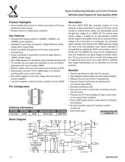
Block Diagram<br />
A2<br />
A1<br />
A0<br />
SDA<br />
SCL<br />
RW REF RL REF V+<br />
V<br />
V SS<br />
INC/DEC<br />
RH REF<br />
AGND V OUT<br />
V DD<br />
V CC CS RH BIAS RW BIAS RL BIAS SHDN<br />
Class A Example<br />
REF<br />
R REF<br />
V SENSE+<br />
C BULK<br />
∆V<br />
V SENSE<strong>–</strong><br />
R SENSE<br />
Comparator<br />
Instrumentation<br />
VP<br />
Amplifier<br />
V REF<br />
choke<br />
I 2 C<br />
control<br />
interface<br />
R BIAS<br />
V bias<br />
control<br />
V BIAS<br />
+<br />
FILTER<br />
Control &<br />
<strong>–</strong><br />
RF<br />
out<br />
Status Registers<br />
RF PA in<br />
EEPROM<br />
Matching<br />
RF Impedance<br />
V BIAS (Unbuffered)<br />
1<strong>–</strong>50<br />
www.xicor.com