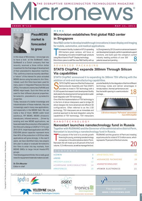
Microvision establishes first global R&D center in ... - I-Micronews
Microvision establishes first global R&D center in ... - I-Micronews
Microvision establishes first global R&D center in ... - I-Micronews
Create successful ePaper yourself
Turn your PDF publications into a flip-book with our unique Google optimized e-Paper software.
THE DISRUPTIVE SEMICONDUCTOR TECHNOLOGIES MAGAZINE<br />
ISSUE N°112 MAY 11, 2011<br />
Copyrights © Yole Développement SA. All rights reserved - Recycled paper<br />
E D I T O R I A L<br />
PiezoMEMS<br />
market is<br />
forecasted<br />
to grow<br />
In this issue of <strong>Micronews</strong>, I encourage you<br />
to have a look at the SolMateS’ news.<br />
SolMateS is a Dutch company that has<br />
recently received a three million dollar<br />
<strong>in</strong>vestment for the f<strong>in</strong>al stage of development<br />
of their piezoelectric deposition mach<strong>in</strong>e.<br />
This confirms a trend we recently identified:<br />
a “reborn” of the <strong>in</strong>terest for piezo actuated<br />
MEMS device us<strong>in</strong>g ferroelectric th<strong>in</strong> films.<br />
Indeed, such th<strong>in</strong> films have been used for<br />
many years <strong>in</strong> Integrated Passives Devices<br />
(IPDs), Ferroelectric memories (FeRAM) and<br />
MEMS <strong>in</strong>kjet heads. Such th<strong>in</strong> films can be<br />
used for their different physical properties:<br />
ferroelectric, piezoelectric or pyroelectric<br />
properties.<br />
Today, because of a better knowledge and<br />
<strong>in</strong>dustrialization of these materials, they are<br />
<strong>in</strong>creas<strong>in</strong>gly used <strong>in</strong> many new applications,<br />
and especially <strong>in</strong> the MEMS field. We can<br />
name a few of them: MEMS wafer level<br />
autofocus, RF MEMS, MEMS ultrasonic<br />
transducers, <strong>in</strong>frared sensors…..Driven by<br />
exist<strong>in</strong>g and new MEMS applications, we<br />
have estimated the production of ferroelectric<br />
th<strong>in</strong> films will undergo a CAGR of +7.5 % over<br />
2010-2015. Inkjet head application and IPDs<br />
ESD/EMI planar capacitor represent more<br />
than 90% of the production <strong>in</strong> 2010 but other<br />
applications will grow strongly. In the next 5<br />
years, we have identified many new players<br />
who plan to adopt or evaluate ferroelectric<br />
th<strong>in</strong> films to enter <strong>in</strong>to key markets, from<br />
MEMS SMEs to large InkJet Heads/IPD<br />
groups.<br />
Yole Développement th<strong>in</strong>ks this is really good<br />
news for equipment/materials makers as well.<br />
Dr. Éric Mounier<br />
Editor-<strong>in</strong>-chief<br />
PLATINUM PARTNERS<br />
MEMS<br />
<strong>Microvision</strong> <strong>establishes</strong> <strong>first</strong> <strong>global</strong> R&D <strong>center</strong><br />
<strong>in</strong> S<strong>in</strong>gapore<br />
New R&D <strong>center</strong> to develop breakthrough <strong>in</strong>novations <strong>in</strong> laser display and imag<strong>in</strong>g<br />
for mobile, automotive, and medical applications.<br />
The research facility, located on NTU's sprawl<strong>in</strong>g<br />
200-hectare green campus, will focus on<br />
develop<strong>in</strong>g <strong>in</strong>novative breakthrough products<br />
us<strong>in</strong>g MicroVision's PicoP ® Display technology.<br />
MicroVision plans to staff the new R&D facility with up<br />
ADVANCED PACKAGING<br />
STATS ChipPAC was one of the fi rst Outsourced<br />
Semiconductor Assembly and Test (OSAT)<br />
providers to <strong>in</strong>vest <strong>in</strong> TSV technology with a<br />
51,000 square foot research and development facility<br />
dedicated to the development of next generation wafer<br />
level <strong>in</strong>tegration with TSV technology.<br />
One of the fi rst implementations of TSV technology is<br />
<strong>in</strong> the form of silicon <strong>in</strong>terposers used to bridge 2D<br />
silicon designs <strong>in</strong>to more advanced and effi cient 3D<br />
configurations. Often referred to as the 2.5D<br />
technology, TSV <strong>in</strong>terposers are an immediate and<br />
practical approach to die level <strong>in</strong>tegration us<strong>in</strong>g the<br />
capabilities of TSV technology. TSV <strong>in</strong>terposers<br />
The purpose of the fund is to provide growth<br />
fi nanc<strong>in</strong>g for young, promis<strong>in</strong>g nanotechnology<br />
companies <strong>in</strong> the adm<strong>in</strong>istrative district Perm.<br />
Nanostart AG will <strong>in</strong>vest up to 25 percent of the fund<br />
volume, 12.5 million euros, as well as manage the fund.<br />
C O N T E N T S<br />
•COWIN 3<br />
•MEMS 8<br />
•MICROFLUIDICS 12<br />
•COMPOUND SEMICONDUCTORS 14<br />
•PHOTONICS 15<br />
to 25 eng<strong>in</strong>eers by 2012 to work on advanced research<br />
and development projects, perform operational support<br />
functions, and build upon the company's current<br />
<strong>in</strong>dustry lead<strong>in</strong>g portfolio of over 500<br />
patents issued and pend<strong>in</strong>g…<br />
STATS ChipPAC expands 300mm Through Silicon<br />
Via capabilities<br />
STATS ChipPAC announced it is expand<strong>in</strong>g its 300mm TSV offer<strong>in</strong>g with the<br />
addition of mid-end manufactur<strong>in</strong>g capabilities.<br />
NANOTECHNOLOGY<br />
provide fl exibility for the <strong>in</strong>tegration of die from different<br />
technology nodes and deliver advantages <strong>in</strong><br />
m<strong>in</strong>iaturisation, thermal performance and<br />
fi ne l<strong>in</strong>e/width spac<strong>in</strong>g <strong>in</strong> a semiconductor<br />
package…<br />
Nanostart launches nanotechnology fund <strong>in</strong> Russia<br />
Together with RUSNANO and the Governor of the adm<strong>in</strong>istrative district Perm,<br />
Nanostart is launch<strong>in</strong>g a nanotechnology fund <strong>in</strong> Russia.<br />
RUSNANO and the governor of Perm are <strong>in</strong>vest<strong>in</strong>g<br />
equal amounts for a total of 37.5 million euros, which<br />
represents 75 percent of the fund volume.<br />
•PHOTOVOLTAIC 16<br />
•ADVANCED PACKAGING 18<br />
•NANOTECHNOLOGY 20<br />
•POWER ELECTRONICS 21<br />
Y O L E D É V E L O P P E M E N T<br />
Free registration on<br />
www.i-micronews.com<br />
8<br />
18<br />
2.5D silicon <strong>in</strong>terposer "PoP module" demonstrator<br />
from STATS ChipPAC<br />
20<br />
1
MAY 2011 issue n°112<br />
THE DISRUPTIVE SEMICONDUCTOR TECHNOLOGIES MAGAZINE<br />
TO MEET US<br />
CS Mantech - Palm Spr<strong>in</strong>gs, CA -<br />
May 17 to 20, 2011<br />
Jo<strong>in</strong> the CS-MANTECH conference at the Hyatt<br />
Grand Champions Resort & Spa and br<strong>in</strong>g<br />
yourself up-to-date on the latest <strong>in</strong> compound<br />
semiconductor (GaAs, GaN, SiC and related<br />
materials) manufactur<strong>in</strong>g processes. Full Details<br />
<strong>in</strong>clud<strong>in</strong>g Advance Program on the website.<br />
PCIM Europe - Nuremberg, Germany -<br />
May 17 to 19, 2011<br />
Visit the lead<strong>in</strong>g show <strong>in</strong> power electronics,<br />
<strong>in</strong>telligent motion and power qualify and have a<br />
look at the comprehensive conference program.<br />
The visit of the exhibtion is free of charge with<br />
pre-registration. From 17 – 19 May 2011,<br />
Nuremberg will be the meet<strong>in</strong>g po<strong>in</strong>t for<br />
<strong>in</strong>ternational experts from science and <strong>in</strong>dustry.<br />
MEPTEC - 9th Annual MEMS Technology<br />
Symposium - San Jose, CA - May 19, 2011<br />
This symposium will br<strong>in</strong>g together experts from<br />
many of these sectors to tell us not only where we<br />
are go<strong>in</strong>g <strong>in</strong> the future, but will also address<br />
specifi c areas that they will need help from<br />
exist<strong>in</strong>g technologies.<br />
ECTC - Lake Buena Vista, FL -<br />
May 31 - June 3, 2011<br />
The premier <strong>in</strong>ternational packag<strong>in</strong>g,<br />
components, and microelectronic systems<br />
technology conference, the Electronic<br />
Components and Technology Conference<br />
(ECTC) strives to offer our attendees an<br />
outstand<strong>in</strong>g array of packag<strong>in</strong>g technology<br />
<strong>in</strong>formation.<br />
GOLD PARTNERS<br />
MICRONEWS FINANCE<br />
Companies compos<strong>in</strong>g the Yole Index, May, 2011<br />
M for Million, MD for Billions<br />
Companies Sector Currency Symbol Price 06/05/11 Price 04/01/11 Price 01/04/10 Price 16/01/09 Price 01/01/07 jan 4 th - may 1 st<br />
ANALOG DEVICES Comp $ ADI.N 40,73 37,52 31,67 19,83 32,87 8,50%<br />
AFFYMETRIX INC Bio Rel Comp $ AFFX.OQ 6,05 4,66 5,9 3,46 23,06 29,80%<br />
AUSTRIAMICROSYSTEMS Comp CHF AMS.S 48,2 45,3 23,45 12,45 84,25 -6,40%<br />
CALIPER LIFE SCI Bio Rel Comp $ CALP.O 6,8 6,11 2,64 1,15 5,72 11,30%<br />
CREE INC Comp $ CREE.O 38,59 66,97 56,84 17,93 17,32 -42,40%<br />
CYPRESS SEMICONDUCTR Comp $ CY.O 21,14 18,24 10,58 4,83 16,87 15,80%<br />
ELMOS SEMICONDUCTOR Comp € ELGG.DE 10,73 9,81 6,85 2,05 7,58 9,30%<br />
HEWLETT PACKARD ( HP ) Comp $ HPQ.N 41,25 43,63 52,45 34,77 41 -5,40%<br />
INFINEON TECH ADS Comp € IFXGn.de 7,91 7,02 4,1 0,94 14,44 12,60%<br />
LAM RESEARCH CP Equipment $ LRCX.O 48,71 49,41 39,88 22,17 50,95 -1,40%<br />
MICRONAS Comp CHF MASN.S 7,96 12,95 4 3,75 26,92 -38,50%<br />
MELEXIS Comp € MLXS.BR 12,5 13,38 6,84 4,90 13,91 -6,50%<br />
MEMSIC Comp $ MEMS.0 3,36 3,21 3,34 1,60 1,7 4,60%<br />
MEMSCAP Comp € MEMS.PA 3,5 4,15 2,26 2,20 21,9 -15,60%<br />
MENTOR GRAPHICS Software $ MENT.O 14,46 11,96 9,25 5,17 18,37 20,90%<br />
NANOGATE Nano tech € N7GG.DE 18,5 15,65 21,9 8,80 34,5 18,20%<br />
NANOPHASE Nano tech $ NANX 1,27 1,26 0,84 0,97 4,9 1,00%<br />
NANOGEN Bio Rel Comp $ NGEN 0,01 0,1 0,2 0,20 1,87 0,00%<br />
OERLIKON Mat/equipt CHF OERL.S 7,1 5,34 4,66 7,40 84,95 33,90%<br />
OKMETIC Material € OKMI.BE 5,46 5,05 3,42 2,46 3,58 8,10%<br />
Copyrights © Yole Développement SA. All rights reserved - Recycled paper<br />
CONSULTING<br />
PLAN OPTIK Material € P40G.DE 3,89 4,06 2,87 1,68 7,35 -4,10%<br />
PSIVIDA LIMITED Bio Rel Comp $ PSDV.OQ 4,12 5,02 3,69 0,99 1,95 -17,90%<br />
Q-CELLS Photovoltaic € QCEG.DE 2,61 2,49 11,39 21,40 34,07 4,80%<br />
RIBER Equipment € RIBE.PA 3,35 2,55 1,3 1,00 2,1 31,30%<br />
SAES GETTERS Materials € SAEI.MI 7,73 6,92 6,1 6,30 27,63 11,70%<br />
SUESS MICROTEC Equipment € SMHG.DE 11,73 9,59 4,4 1,37 6,95 37,80%<br />
SOITEC Material € SOIT.PA 10,44 8,51 10,77 2,92 27,72 22,60%<br />
SUNPOWER CORPORATION Photovoltaic $ SPWRA 21,34 13,63 23,95 33,62 37,17 56,50%<br />
STMICROELECTRONICS Comp € STM.PA 7,91 8,1 6,48 4,29 14,07 -2,30%<br />
PVA TEPLA Equipment € TPEG.DE 4,36 3,91 5,37 2,59 28,45 11,50%<br />
TESSERA Equipment $ TSRA.O 18,83 21,7 23,81 11,32 4,37 -13,20%<br />
TEXAS INSTRUMENTS Comp $ TXN.N 35,36 32,67 26,01 15,02 40,34 8,20%<br />
ULTRATECH INC Equipment $ UTEK.O 30,26 19,27 15,37 10,60 12,48 57,10%<br />
F<strong>in</strong>d more details on www.I-micronews.com<br />
Comp for components, Bio Comp for Bio related component, Nano tech for Nanotechnologies<br />
2
MAY 2011 issue n°112<br />
THE DISRUPTIVE SEMICONDUCTOR TECHNOLOGIES MAGAZINE<br />
COWIN<br />
COWIN Marketplace - 14 th -16 th June 2011, Scandic Mar<strong>in</strong>a Congress <strong>in</strong> Hels<strong>in</strong>ki<br />
Come to COWIN Marketplace to know more about available technologies, on-go<strong>in</strong>g <strong>in</strong>novative projects and fund<strong>in</strong>g<br />
opportunities <strong>in</strong> smart systems. COWIN is a support action to optimize value creation from European collaborative<br />
research results <strong>in</strong> generat<strong>in</strong>g bus<strong>in</strong>ess opportunities.<br />
From Smart phones to smart <strong>in</strong>dustrial processes, the trend is set.<br />
M<strong>in</strong>iaturised smart systems are becom<strong>in</strong>g more and more key components<br />
<strong>in</strong> our private and professional lives. They enable better telecommunications,<br />
energy effi ciency, susta<strong>in</strong>able transport, fast and reliable medical diagnostics,<br />
breakthroughs <strong>in</strong> healthcare, <strong>in</strong>novative enterta<strong>in</strong>ment…<br />
Whatever the doma<strong>in</strong> of activity, the market is already ask<strong>in</strong>g for M<strong>in</strong>iaturised<br />
Smart Systems.<br />
To optimise your <strong>in</strong>novation process, jo<strong>in</strong> the European network and meet with<br />
future key partners. Take the chance to access available resources and most of<br />
all to start <strong>in</strong>teractions with the most suitable operational and fi nancial resources<br />
related to your needs.<br />
COWIN Marketplace will be composed of 3 events which participation is<br />
free of charge:<br />
• An <strong>in</strong>formation session on “F<strong>in</strong>anc<strong>in</strong>g major milestones from R&D to market"<br />
will gather representatives from the European Commission, from the European<br />
Technology Platform EPoSS, from the <strong>in</strong>vestors community and from<br />
EURIPIDES <strong>in</strong> order to provide the audience with key elements on support<br />
<strong>in</strong>itiatives all along the technology value cha<strong>in</strong>.<br />
14 th June 2011 from 15:00 to 17:30, Room FENNIA I<br />
• Personal contacts are essential for successful co-operations. COWIN is<br />
organis<strong>in</strong>g a matchmak<strong>in</strong>g event consist<strong>in</strong>g <strong>in</strong> <strong>in</strong>dividual meet<strong>in</strong>gs between<br />
technology providers, <strong>in</strong>tegrators and bus<strong>in</strong>ess partners <strong>in</strong> order to foster<br />
<strong>in</strong>novation and to discuss on concrete bus<strong>in</strong>ess opportunities. COWIN will give<br />
you the chance to optimise your meet<strong>in</strong>gs schedule accord<strong>in</strong>g to your needs.<br />
14 th -16 th June 2011, Room NORDIA<br />
• A posters exhibition is the actual core of COWIN Marketplace. In this common<br />
Euripides-COWIN area, <strong>in</strong>novative research results from FP6-FP7 projects but<br />
also on-go<strong>in</strong>g projects under the EURIPIDES programme will be given the fl oor<br />
to present themselves and to raise <strong>in</strong>terests among the audience for further<br />
partnerships. The poster presenters will be available for questions and<br />
discussions. Furthermore exhibitors will have the opportunity to br<strong>in</strong>g<br />
demonstrators to emphasise the impact of the posters.<br />
14 th -16 th June 2011, Room NORDIA<br />
to<br />
me<br />
About the Smart System Week<br />
The Smart System Week will take place at the Scandic Mar<strong>in</strong>a Congress <strong>in</strong><br />
Hels<strong>in</strong>ki from 14 th to 17 th June 2011. The EURIPIDES Cluster, <strong>in</strong> close cooperation<br />
with VTT and TEKES, will present its 5 th Annual Forum, highlight new trends <strong>in</strong><br />
Technology and Bus<strong>in</strong>ess and gather the Smart System Community with<br />
dedicated events aim<strong>in</strong>g at generat<strong>in</strong>g ideas for future bus<strong>in</strong>esses.<br />
A series of workshops will take place on the 14 th June:<br />
• The EPoSS Key Technologies Work<strong>in</strong>g Group will organise a practical workshop<br />
to elaborate and prepare expression of <strong>in</strong>terests (EOI) and project ideas.<br />
• The Eemeli Workshop, supported by TEKES and VTT, will focus on help<strong>in</strong>g<br />
SMEs to get access to Smart Systems Technologies as well as to network<br />
<strong>in</strong>ternationally and to learn to use European fund<strong>in</strong>g schemes <strong>in</strong> creat<strong>in</strong>g new<br />
competitive advantages.<br />
• Easy access to Microsystems production through contract manufactur<strong>in</strong>g<br />
services organised by VTT Memsfab. Purpose of the event is to promote<br />
<strong>in</strong>creas<strong>in</strong>g use of Microsystems, to bridge the gap from lab-to-fab and to offer<br />
an opportunity to meet foundries.<br />
Technical visits will be organised on 17 th June 2011:<br />
Two tours (tour 1: Nokia Research Center, Micronova or tour 2: VTI Technologies,<br />
Okmetic) will give an overview of Key F<strong>in</strong>nish research sites as well as <strong>in</strong>dustrial<br />
facilities.<br />
Mrs. Gérald<strong>in</strong>e Andrieux Gust<strong>in</strong><br />
Mr. Nicolas Gouze<br />
COWIN Coord<strong>in</strong>ator<br />
COWIN Communication<br />
c/o Yole Développement<br />
c/o VDI/VDE- Innovation + Technik<br />
andrieux@yole.fr<br />
nicolas.gouze@vdivde-it.de<br />
Tel. : +33 6 75 800 829 Tel.: +49 30 310078-209<br />
www.cow<strong>in</strong>4u.eu<br />
About COWIN<br />
COWIN is a support action launched under the 7 th framework Program for 3 years to strengthen the European competitiveness <strong>in</strong> m<strong>in</strong>iaturized smart systems.<br />
This <strong>in</strong>itiative is dedicated to the commercial exploitation of advanced technologies developed <strong>in</strong> the framework of European collaborative research projects.<br />
COWIN’s mission is to facilitate take-up of the advanced technologies worthy of <strong>in</strong>vestments, <strong>in</strong> order to capture <strong>in</strong>novation, w<strong>in</strong> new markets and make a profi t.<br />
A Smart System Week <strong>in</strong> Hels<strong>in</strong>ki for<br />
Creat<strong>in</strong>g Innovations and Bus<strong>in</strong>ess<br />
Copyrights © Yole Développement SA. All rights reserved - Recycled paper<br />
3
MAY 2011 issue n°112<br />
THE DISRUPTIVE SEMICONDUCTOR TECHNOLOGIES MAGAZINE<br />
CALL FOR PAPERS<br />
MEMS – Enter<strong>in</strong>g a New Growth Cycle!<br />
The SEMICON Europe 2011 is the perfect platform for all players <strong>in</strong> the MEMS/MST <strong>in</strong>dustry. The show will be <strong>in</strong> Dresden/<br />
Germany from 11 – 13 October.<br />
The development of the MEMS Market is hardly<br />
to be overlooked. With a 22 % growth <strong>in</strong> 2010,<br />
the MEMS and Sensor Market is back on track<br />
aga<strong>in</strong>. Accord<strong>in</strong>g to reliable prognoses this trend will<br />
further extend until 2015.<br />
The new growth stands on a solid basis and several<br />
reasons support that this may be a long-term<br />
development:<br />
• MEMS markets for consumer electronics and<br />
mobile phones will grow at an accelerated rate over<br />
the next 4 years, <strong>in</strong> particular revenue for handsets<br />
and slate tablets.<br />
• The soar<strong>in</strong>g demand for MEMS sensors from BRIC<br />
countries (Brasil, Russia, India and Ch<strong>in</strong>a) <strong>in</strong> all<br />
sectors from cars to <strong>in</strong>frastructure e.g. for smart<br />
meters and optical telecom is driv<strong>in</strong>g demand.<br />
• Sales of DLP chips (Digital Light Process<strong>in</strong>g) were<br />
aga<strong>in</strong> up <strong>in</strong> 2010.<br />
• Increas<strong>in</strong>g use of sensors <strong>in</strong> address<strong>in</strong>g critical<br />
areas like energy and ag<strong>in</strong>g population.<br />
Therefore, the relevance of the International<br />
MEMS/MST Industry Forum on the SEMICON<br />
Europa 2011 cannot be underestimated. The Forum<br />
takes focus on the key success factors of the new<br />
growth cycle:<br />
• An area of new <strong>in</strong>terest<strong>in</strong>g applications promotes<br />
new technologies and provides l<strong>in</strong>e utilization;<br />
• Successful management of distributed operations<br />
<strong>in</strong>clud<strong>in</strong>g foundries, with methodologies for steep<br />
learn<strong>in</strong>g curves, best system know-how and ever<br />
shorter time-to-revenue cycles;<br />
• Effi cient high volume test<strong>in</strong>g and quality assurance;<br />
• Innovative <strong>in</strong>tegration concepts for complex sensor<br />
systems.<br />
The MEMS applications will be the centre of<br />
attraction for many visitors: What will be their future<br />
usage <strong>in</strong> the automotive <strong>in</strong>dustry, biomedic<strong>in</strong>e and<br />
life science, consumer electronics, optical<br />
telecommunication and also <strong>in</strong> high-end areas like<br />
aeronautics and <strong>in</strong>dustrial manufactur<strong>in</strong>g?<br />
Additionally, the conference will cover all standard<br />
parts which are important for the day-to-day<br />
<strong>in</strong>dustrial production. The current leverage of the<br />
standardization, test<strong>in</strong>g methods and results as well<br />
as strategies for high added volume and emerg<strong>in</strong>g<br />
products will be <strong>in</strong> the focus dur<strong>in</strong>g the show.<br />
The range of the conference conta<strong>in</strong>s the know-how<br />
of technical processes and new materials for the<br />
MEMS <strong>in</strong> front-end, back-end and test<strong>in</strong>g. This<br />
technical part deals with 3D and TSV (through silicon<br />
via) processes. Different Chip and WLP (wafer level<br />
package) technologies are also part of the program.<br />
Another session deals with the MEMS application<br />
markets, the chances and risks but also with<br />
forecasts and outlook.<br />
For <strong>in</strong>formation on SEMICON Europa 2011,<br />
please visit www.semiconeuropa.org<br />
or contact Carlos Lee, per email clee@semi.org<br />
or per telephone: +32 2 6095334<br />
Copyrights © Yole Développement SA. All rights reserved - Recycled paper<br />
4
MAY 2011 issue n°112<br />
THE DISRUPTIVE SEMICONDUCTOR TECHNOLOGIES MAGAZINE<br />
INDUSTRY OUTLOOK<br />
“ Permanent Wafer Bond<strong>in</strong>g will be a key enabl<strong>in</strong>g technology for<br />
advanced semiconductor manufactur<strong>in</strong>g” says Yole Développement<br />
Yole Développement announces the publication of its technology study and market research report, Permanent Wafer<br />
Bonders Applications & Market Report.<br />
Historically developed for MEMS & SOI substrates, the wafer bond<strong>in</strong>g technology is today becom<strong>in</strong>g a key process<strong>in</strong>g<br />
technology for a wide range of applications: MEMS, CMOS Image Sensors, LEDs, Power Devices, RF and Advanced<br />
Packag<strong>in</strong>g. The wafer bond<strong>in</strong>g market is a very complex one cross<strong>in</strong>g different wafer sizes (from 2’’ to 12’’), different<br />
applications and different bond<strong>in</strong>g technologies.<br />
Market overview<br />
Wafer bond<strong>in</strong>g is usually defi ned as a process that<br />
temporarily or permanently jo<strong>in</strong>s two wafers or<br />
substrates us<strong>in</strong>g a suitable process. Historically<br />
developed for MEMS and then SOI wafers, wafer<br />
bond<strong>in</strong>g technology has shifted to non-ma<strong>in</strong>stream<br />
IC applications over the last years. Our report aims<br />
at analyz<strong>in</strong>g the market perspectives and technical<br />
trends for permanent bond<strong>in</strong>g.<br />
“MEMS have been the fi rst application where wafer<br />
bonders have been massively used (the wafer<br />
bond<strong>in</strong>g step is mostly used to protect the MEMS<br />
sensitive element). And CMOS Image Sensors is<br />
also a very large market for wafer bonders”, expla<strong>in</strong>ed<br />
Dr Eric Mounier, Project Manager at Yole<br />
Développement.<br />
But besides MEMS and CIS, wafer bonder can be<br />
also used for LEDs or Power Devices. Indeed, <strong>in</strong> a<br />
typical LED active region, spontaneous emission<br />
scatters photons <strong>in</strong> all directions. If the substrate<br />
material has a smaller band gap than the active<br />
region, approximately half of the light is absorbed <strong>in</strong><br />
the substrate; significantly reduc<strong>in</strong>g device<br />
performance. So, one of the manufactur<strong>in</strong>g solutions<br />
for photon loss <strong>in</strong>volves bond<strong>in</strong>g a wafer conta<strong>in</strong><strong>in</strong>g<br />
an array of devices to another wafer that provides<br />
both a refl ective surface for maximum light extraction<br />
and a heat s<strong>in</strong>k for thermal management. And of<br />
course, over the 5 past years, much attention has<br />
been given to this technology for 3D <strong>in</strong>tegration of<br />
memories for example.<br />
Technology challenges<br />
For MEMS, there is today a shift from Glass Frit for<br />
eutectic/metal-based bond<strong>in</strong>g ma<strong>in</strong>ly to <strong>in</strong>crease<br />
real estate by smaller bond frames. Metal direct<br />
bond<strong>in</strong>g also gives good hermeticity and mechanical<br />
stability for many MEMS applications. For example,<br />
Nasiri process is us<strong>in</strong>g eutectic bond<strong>in</strong>g of the MEMS<br />
directly on the alum<strong>in</strong>um layer of the CMOS wafer.<br />
This leads to smaller package footpr<strong>in</strong>ts & package<br />
heights. STMicroelectronics’ latest 3-axis<br />
accelerometer also shows a different seal<strong>in</strong>g<br />
technique compared to what is usually done: gold<br />
eutectic seal<strong>in</strong>g allows a dramatic die size reduction.<br />
For CMOS Image sensors, the advent of the BSI<br />
(Back Side Illum<strong>in</strong>ation) technology has raised a<br />
competition between Molecular Bond<strong>in</strong>g and<br />
adhesive bond<strong>in</strong>g. Here, cost and fi nal application<br />
will drive the technology fi nal choice.<br />
Yole Développement has estimated the wafer bonder<br />
to have big market growth for the next year. The<br />
growth will be driven small size wafer for LEDs and<br />
12” wafer for 3D stack<strong>in</strong>g and CIS.<br />
Yole Développement’s report analyzes <strong>in</strong> details the<br />
technical & economical evolution of the permanent<br />
wafer bond<strong>in</strong>g process. It gives, for example, 2010-<br />
2016 market forecasts for permanent bond<strong>in</strong>g,<br />
number of equipment, an overview of the different<br />
bond<strong>in</strong>g approaches and equipment players market<br />
shares.<br />
It describes the applications for wafer bond<strong>in</strong>g with<br />
ma<strong>in</strong> characteristics, challenges and technical<br />
trends.<br />
For more <strong>in</strong>formation about Yole Développement reports,<br />
please contact D. Jourdan (jourdan@yole.fr)<br />
Permanent Wafer Bond<strong>in</strong>g Applications<br />
(Source: Yole Développement, May 2011)<br />
Accelerometers<br />
1st level packag<strong>in</strong>g<br />
Microbolometers<br />
Gyros<br />
SGOI<br />
SOQ<br />
Optical MEMS<br />
Microphones<br />
Pressure sensor<br />
Microfluidics<br />
IGBTs<br />
Resonators<br />
RF MEMS<br />
Stress isolation/<br />
device<br />
manufactur<strong>in</strong>g<br />
Th<strong>in</strong> films LEDs<br />
Power<br />
MEMS<br />
LEDs<br />
Wafer<br />
Bond<strong>in</strong>g<br />
Advanced<br />
substrates<br />
RF<br />
Devices<br />
Advanced<br />
Packag<strong>in</strong>g<br />
CMOS<br />
Image<br />
Sensors<br />
SOI<br />
GOI<br />
Encapsulation<br />
Interposers<br />
FO WLP<br />
Microbumps<br />
MMIC<br />
3D ICs<br />
5Copyrights © Yole Développement SA. All rights reserved - Recycled paper
Copyrights © Yole Développement SA. All rights reserved.<br />
Copyrights © Yole Développement SA. All rights reserved.<br />
Copyrights © Yole Développement SA. All rights reserved - Recycled paper<br />
MAY 2011 issue n°112<br />
ONLINE EVENT<br />
Register for a live webcast today:<br />
Revolution <strong>in</strong> consumer motion sensors<br />
Jo<strong>in</strong> Yole Développement’s expert, Laurent Rob<strong>in</strong>, on<br />
Tuesday, 31 st of May at 5.30 pm CET to learn about motion<br />
sensors.<br />
Visit our website www.i-<strong>Micronews</strong>.com, webcast section,<br />
to register.<br />
The <strong>in</strong>ertial sensor market for consumer electronics is grow<strong>in</strong>g very quickly<br />
due the fast adoption of accelerometers, gyroscopes and magnetometers<br />
<strong>in</strong> mobile phones, tablets, game stations, laptops…. Indeed 20.3% annual<br />
growth is expected: from $847M <strong>in</strong> 2009, the motion sensor market will reach<br />
$2.56B <strong>in</strong> 2015! The MEMS accelerometer market will show very nice bus<strong>in</strong>ess<br />
opportunities <strong>in</strong> the com<strong>in</strong>g years. Moreover this market will be strategic because<br />
many applications are expected to rely on 3-axis accelerometer + 3-axis gyroscope<br />
<strong>in</strong> a s<strong>in</strong>gle package with<strong>in</strong> 2015. There is thus a strong synergy between<br />
accelerometer and gyroscope technologies and players…<br />
•<br />
•<br />
•<br />
•<br />
FREE OF CHARGE WEBCAST<br />
© 2011 • 6<br />
2009-2015 Market Overview<br />
Overview<br />
The market for motion sensors is grow<strong>in</strong>g to<br />
more than $2.5B <strong>in</strong> 2015, correspond<strong>in</strong>g to<br />
4.5B sensor packages<br />
– One sensor package can conta<strong>in</strong> several sensors<br />
(combo sensors) market is actually 5.18B sens<strong>in</strong>g<br />
functions <strong>in</strong> 2015<br />
– 15.7% 2009-2015 CAGR <strong>in</strong> value, 24.4% <strong>in</strong> volume<br />
Mobile phone and gam<strong>in</strong>g are the biggest CE<br />
markets for motion sensors and combo<br />
sensors<br />
Remote control application will emerge<br />
slowly, with gam<strong>in</strong>g functions as a key feature<br />
Very high potential <strong>in</strong> the sports area, but it<br />
will take time to emerge, and it is a collection<br />
of plenty of niche applications<br />
<br />
<br />
<br />
<br />
<br />
<br />
<br />
<br />
<br />
<br />
<br />
<br />
<br />
<br />
<br />
<br />
<br />
<br />
<br />
<br />
<br />
<br />
MEMS Gyroscopes for Mobile Phones<br />
What’s next for gyropscopes after iPhone 4?<br />
• Now that appropriate Android drivers seem available, we start to see that the major<br />
handset makers release few models with gyroscopes<br />
Samsung Galaxy<br />
• Samsung Galaxy S Pro: <strong>first</strong> Android phone with a gyroscope?<br />
S Pro<br />
– Rumors said that this phone <strong>in</strong>tegrates a gyroscope. But it has not been confirmed<br />
– Also features an accelerometer, AGPS, compass<br />
– Named Epic 4G <strong>in</strong> USA, released by Spr<strong>in</strong>t<br />
• Released beg<strong>in</strong>n<strong>in</strong>g 2011, the Google Nexus S <strong>in</strong>tegrates a gyro<br />
– This confirms the adoption of gyroscopes <strong>in</strong> high-end smartphones<br />
• LG Optimus Black: <strong>first</strong> handset design w<strong>in</strong> for InvenSense!<br />
Google Nexus S<br />
– This smartphone will <strong>in</strong>tegrate InvenSense’s ITG-3200 3 axis MEMS gyroscope for (manufactured by<br />
nice user <strong>in</strong>terface functions<br />
Samsung)<br />
– This design-w<strong>in</strong> from InvenSense on an Android phone shows that ST can expect<br />
strong competition<br />
• Other mobile phone makers:<br />
– HTC has revealed that they will release a gyroscope-equipped smartphone <strong>in</strong> mid<br />
2010<br />
LG Optimus<br />
– June 2010: the director of Motorola mobile division has announced that they are<br />
Black<br />
will<strong>in</strong>g to release a smartphone with a gyro by the end of 2010. But such a product<br />
has not been seen on the market yet.<br />
– Sony Ericsson<br />
© 2011 – • 11 <br />
Therefore Yole Developpement is pleased to organize a webcast on this topic. The<br />
webcast entitled “Revolution <strong>in</strong> Consumer Motion Sensors” will be presented by<br />
Laurent Rob<strong>in</strong>, Market & Technology Analyst, on Tuesday, 31 st of May at 5.30 pm CET.<br />
Register NOW on I-<strong>Micronews</strong>.com, webcast section.<br />
For more <strong>in</strong>formation about the webcast, please contact David Jourdan (jourdan@yole.fr)<br />
Organized by<br />
Speaker:<br />
Laurent Rob<strong>in</strong> is <strong>in</strong> charge of the MEMS & Sensors market<br />
research at Yole Developpement. He previously worked<br />
at image sensor company e2v Technologies (Grenoble,<br />
France) and at EM Microelectronics (Switzerland). He<br />
holds a Physics Eng<strong>in</strong>eer<strong>in</strong>g degree from the National<br />
Institute of Applied Sciences <strong>in</strong> Toulouse. He was also<br />
granted a Master Degree <strong>in</strong> Technology & Innovation<br />
Management from EM Lyon Bus<strong>in</strong>ess School, France.<br />
<br />
<br />
<br />
<br />
<br />
<br />
<br />
Hosted by<br />
THE DISRUPTIVE SEMICONDUCTOR TECHNOLOGIES MAGAZINE<br />
MEMS MARKET BRIEFING<br />
AT TRANSDUCERS 2011<br />
FREE ENTRANCE<br />
Mobile phone<br />
& consumer<br />
electronics are driv<strong>in</strong>g<br />
the growth of the<br />
MEMS bus<strong>in</strong>ess...<br />
Evolutions <strong>in</strong> the microphone<br />
and motion sensor market<br />
June 7, at Transducers 2011<br />
At 6.30 PM<br />
6.30 PM - MEMS market forecasts :<br />
where is the MEMS <strong>in</strong>dustry head<strong>in</strong>g?<br />
Jean-Christophe Eloy,<br />
President & CEO, Yole Développement<br />
7.00 PM - MEMS microphone market:<br />
evolution of bus<strong>in</strong>ess models and supply cha<strong>in</strong><br />
Wenb<strong>in</strong> D<strong>in</strong>g,<br />
MEMS Market & Technology Analyst, Yole Développement<br />
7.30 PM - Revolution <strong>in</strong> consumer motion sensors<br />
Jean-Christophe Eloy,<br />
President & CEO, Yole Développement<br />
8.00 PM - Network<strong>in</strong>g cocktail<br />
Y O L E D É V E L O P P E M E N T<br />
For more <strong>in</strong>formation,<br />
please contact<br />
Sandr<strong>in</strong>e Leroy<br />
(leroy@yole.fr)<br />
6
7<br />
MAY 2011 issue n°112<br />
THE DISRUPTIVE SEMICONDUCTOR TECHNOLOGIES MAGAZINE<br />
It’s not who you know today.<br />
It’s who you’re go<strong>in</strong>g to need to know tomorrow.<br />
The world of <strong>in</strong>ertial devices is <strong>in</strong> a rapid state of change. Value is shift<strong>in</strong>g.<br />
Players are chang<strong>in</strong>g. The entire <strong>in</strong>dustry of motion is <strong>in</strong> motion. While we all<br />
know the current players, our growth depends on meet<strong>in</strong>g and engag<strong>in</strong>g the<br />
emerg<strong>in</strong>g <strong>in</strong>novators.<br />
The world leader <strong>in</strong> MEMS technology <strong>in</strong>formation, Yole Développement, is harness<strong>in</strong>g<br />
the power and effi ciency of an excit<strong>in</strong>g new network<strong>in</strong>g and collaboration<br />
event. Not another tradeshow or conference, the MEMS <strong>in</strong> Motion Collaboration<br />
Summit promises the freedom to meet, learn, talk, and ultimately collaborate <strong>in</strong> a<br />
time-effi cient and casual environment.<br />
The Yole team will br<strong>in</strong>g together <strong>in</strong>dustry leaders for this fi rst-of-a-k<strong>in</strong>d, two-day<br />
event <strong>in</strong> Palm Spr<strong>in</strong>gs. Qualifi ed attendees will enjoy exclusive Yole plenary<br />
sessions; small, facilitated roundtable discussions; and hours of small group and<br />
one-on-one discussion activities.<br />
If your bus<strong>in</strong>ess depends on—or will depend on—<strong>in</strong>ertial devices, the MEMS <strong>in</strong><br />
Motion Collaboration Summit is perfect for you.<br />
Shape the future of <strong>in</strong>ertial devices at the<br />
MEMS <strong>in</strong> Motion Collaboration Summit<br />
OCTOBER 12-13, 2011<br />
Palm Spr<strong>in</strong>gs, CA USA<br />
Information@MEMS<strong>in</strong>Motion.com<br />
www.MEMS<strong>in</strong>Motion.com<br />
Copyrights © Yole Développement SA. All rights reserved - Recycled paper
MAY 2011 issue n°112<br />
THE DISRUPTIVE SEMICONDUCTOR TECHNOLOGIES MAGAZINE<br />
MEMS<br />
<strong>Microvision</strong> <strong>establishes</strong> <strong>first</strong> <strong>global</strong> R&D <strong>center</strong> <strong>in</strong> S<strong>in</strong>gapore<br />
From page 1<br />
By collaborat<strong>in</strong>g with NTU, MicroVision aims<br />
to leverage the university's strength and<br />
expertise <strong>in</strong> Eng<strong>in</strong>eer<strong>in</strong>g, Microelectronics<br />
and Materials Science to conduct jo<strong>in</strong>t research and<br />
development with faculty and students.<br />
MicroVision's dedicated R&D <strong>center</strong> <strong>in</strong>cludes a<br />
customized laboratory at NTU's Innovation Centre.<br />
The company will work directly with NTU's School of<br />
Electrical and Electronic Eng<strong>in</strong>eer<strong>in</strong>g and the<br />
Division of Physics and Applied Physics.<br />
NTU has established strong <strong>in</strong>dustry partners<br />
<strong>in</strong>clud<strong>in</strong>g Rolls-Royce, Robert Bosch, Thales, and<br />
Toray. Like MicroVision, these lead<strong>in</strong>g companies<br />
chose to set up research facilities at NTU, where they<br />
collaboratively work with NTU faculty and students<br />
to pursue their respective research <strong>in</strong>terests.<br />
www.microvision.com<br />
DelfMEMS successfully delivered custom RF MEMS samples to NTT DOCOMO<br />
DelfMEMS has provided arrays of custom MEMS ohmic switches to enable tunability <strong>in</strong>to Radio-Frequency front-end<br />
modules -FEM- for mobile applications.<br />
Voltage, size, losses, isolation, ultra-fast<br />
switch<strong>in</strong>g time and power handl<strong>in</strong>g will be<br />
evaluated by the <strong>in</strong>novative telecom operator<br />
accord<strong>in</strong>g to the requested specifications until 6 GHz.<br />
DelfMEMS is sett<strong>in</strong>g-up an open technology platform<br />
to propose a new <strong>in</strong>tegrated micro-mechanical<br />
build<strong>in</strong>g block that is based on a strong, totally new<br />
IP portfolio that solves past issues of RF MEMS ohmic<br />
switches. MEMS switch is considered as the optimum<br />
RF switch<strong>in</strong>g technology that drastically decreases<br />
power consumption and bill of material by m<strong>in</strong>imiz<strong>in</strong>g<br />
losses between the antenna and active devices of a<br />
FEM.<br />
www.delfmems.com<br />
Lemoptix MEMS micromirrors replace galvanometer and rotat<strong>in</strong>g mirrors<br />
Optical MEMS scann<strong>in</strong>g micromirrors much smaller, much faster, much more robust and much less power<br />
consum<strong>in</strong>g than conventional optical scann<strong>in</strong>g systems.<br />
Lemoptix silicon-based, magnetically actuated<br />
MEMS micromirror technologies are best <strong>in</strong><br />
class replacement solutions to traditional<br />
galvanometer and rotat<strong>in</strong>g mirrors, br<strong>in</strong>g<strong>in</strong>g<br />
outstand<strong>in</strong>g performance and space reduction.<br />
Respond<strong>in</strong>g to <strong>in</strong>dustry requests to significantly<br />
reduce size, power consumption and <strong>in</strong>creased<br />
performance of micromirror devices, Lemoptix has<br />
developed a bottom-up approach by us<strong>in</strong>g semiconductor-like<br />
equipment to build micromirrors with<br />
actuation based on magnetic and heat-dissipat<strong>in</strong>g<br />
pr<strong>in</strong>ciples <strong>in</strong>stead of gear<strong>in</strong>gs.<br />
Lemoptix LSCAN laser scann<strong>in</strong>g micromirrors are<br />
<strong>in</strong>tegrated by OEM customers <strong>in</strong>to a number of<br />
immediately available applications like optical<br />
spectrometers, laser range f<strong>in</strong>ders and microscopes,<br />
enhanc<strong>in</strong>g performances and enabl<strong>in</strong>g the<br />
development of smaller, higher resolution and lower<br />
cost products. Lemoptix’ resonant and static<br />
scann<strong>in</strong>g micromirrors are designed to rotate and<br />
deflect light and can be used <strong>in</strong> a myriad of optical<br />
applications due to the unique comb<strong>in</strong>ation of<br />
performance and size.<br />
www.optoiq.com<br />
LSCAN-F series (Resonant) (Courtesy of Lemoptix)<br />
Copyrights © Yole Développement SA. All rights reserved - Recycled paper<br />
Okmetic <strong>in</strong>creases SOI wafer production capacity <strong>in</strong> Vantaa and specifies<br />
long-term f<strong>in</strong>ancial objectives<br />
Okmetic's board of directors has approved plans to <strong>in</strong>crease the group's silicon-on-<strong>in</strong>sulator (SOI) wafer production<br />
capacity by extend<strong>in</strong>g the Vantaa plant.<br />
The around 30 million euro <strong>in</strong>vestment <strong>in</strong>cludes<br />
the plant extension and different k<strong>in</strong>ds of<br />
production equipment. This <strong>in</strong>vestment,<br />
together with the on-go<strong>in</strong>g SOI equipment<br />
<strong>in</strong>vestments, more than triples the Vantaa plant's<br />
current SOI wafer production capacity. Along with the<br />
grow<strong>in</strong>g production amounts, new equipment and<br />
process development, improved productivity is be<strong>in</strong>g<br />
aimed at. At the same time, improvement of SOI<br />
wafers' performance cont<strong>in</strong>ues <strong>in</strong> order to ensure<br />
customers' competitiveness.<br />
The <strong>in</strong>vestment will be carried out ma<strong>in</strong>ly <strong>in</strong> 2011-<br />
2013. The build<strong>in</strong>g of the Vantaa plant extension will<br />
start <strong>in</strong> autumn 2011. The surface area of the<br />
extension is 2,420 m2, approximately a quarter of<br />
which is for clean room facilities. The extension is<br />
due to be complete <strong>in</strong> the end of 2012, after which it<br />
will be taken <strong>in</strong>to production use <strong>in</strong> stages, follow<strong>in</strong>g<br />
the growth of the market demand.<br />
The aim is that the <strong>in</strong>vestment will be covered ma<strong>in</strong>ly<br />
with cash flow from operations, and no need for<br />
significant loan f<strong>in</strong>anc<strong>in</strong>g is foreseeable.<br />
SOI wafers are used for demand<strong>in</strong>g MEMS sensors<br />
and HV applications whose markets have <strong>in</strong>creased<br />
year by year. It is estimated that the markets cont<strong>in</strong>ue<br />
to grow as automotive electronics, consumer<br />
electronics as well as <strong>in</strong>dustrial process control<br />
<strong>in</strong>crease. Sensor applications <strong>in</strong>crease especially <strong>in</strong><br />
consumer products such as smart phones, cameras,<br />
game consoles and <strong>in</strong> other portable devices.<br />
This newly made <strong>in</strong>vestment decision supports<br />
Okmetic's long-term strategy and growth objectives,<br />
strengthens company's market leadership as the<br />
supplier of demand<strong>in</strong>g sensor wafers and enables<br />
<strong>in</strong>crease of market share <strong>in</strong> SOI wafers.<br />
www.reuters.com<br />
8
9<br />
MAY 2011 issue n°112<br />
THE DISRUPTIVE SEMICONDUCTOR TECHNOLOGIES MAGAZINE<br />
MEMS<br />
New MEMS microphones from<br />
STMicroelectronics enhance audio<br />
experience <strong>in</strong> mobile phones and<br />
portable computers<br />
STMicroelectronics <strong>in</strong>troduced two new digital MEMS<br />
microphones.<br />
October 2 to 5, 2011<br />
MP34DB01 and MP45DT02 microphones (Courtesy of STMicroelectronics)<br />
Comb<strong>in</strong><strong>in</strong>g superior sound quality with robustness and reliability at reduced<br />
size and cost, ST’s MP34DB01 and MP45DT02 microphones enable<br />
enhanced audio experience <strong>in</strong> mobile phones and portable computers, as<br />
well as <strong>in</strong> many other exist<strong>in</strong>g and emerg<strong>in</strong>g applications with a voice <strong>in</strong>put.<br />
ST’s MEMS microphones use best-<strong>in</strong>-class acoustic sensor technology jo<strong>in</strong>tly<br />
developed with OMRON that is <strong>in</strong>herently less susceptible to mechanical vibration,<br />
temperature variations and electromagnetic <strong>in</strong>terference, while provid<strong>in</strong>g high-fidelity<br />
reproduction of audio signals. Integrat<strong>in</strong>g ST’s electronic control circuit and OMRON’s<br />
micro-mach<strong>in</strong>ed sensor <strong>in</strong> a s<strong>in</strong>gle package, the microphones deliver superb audio<br />
performance at lower power consumption than traditional condenser (ECM)<br />
microphones. This optimized power consumption ensures longer battery life <strong>in</strong><br />
portable devices for an extended user experience.<br />
In addition to the size, robustness and energy economy advantages over ECM<br />
microphones, MEMS microphones enable dramatic advancements <strong>in</strong> sound quality,<br />
realized by <strong>in</strong>corporat<strong>in</strong>g multiple microphones <strong>in</strong> one device. Such microphone<br />
arrays, facilitated by the small form factor, superior sensitivity match<strong>in</strong>g and frequency<br />
response of ST’s microphones, enable the implementation of active noise and echo<br />
cancell<strong>in</strong>g, as well as beam-form<strong>in</strong>g, a sound-process<strong>in</strong>g technology that helps<br />
isolate a sound and its location. These features are valuable with the <strong>in</strong>creas<strong>in</strong>g use<br />
of cell phones and other devices <strong>in</strong> noisy and uncontrollable environments.<br />
Another important factor <strong>in</strong> multiple-microphone applications is the high temperature<br />
stability of MEMS microphones after reflow that ensures ample flexibility <strong>in</strong> plac<strong>in</strong>g<br />
the auxiliary microphones, <strong>in</strong>clud<strong>in</strong>g <strong>in</strong> locations with higher temperature excursions.<br />
ST’s MP34DB01 microphone is the only device <strong>in</strong> the market with real high-fidelity<br />
audio bandwidth, deliver<strong>in</strong>g flat frequency response <strong>in</strong> the full audio band of 20–<br />
20,000 Hz, coupled with an unparalleled signal-to-noise ratio (62 dB) and powersupply<br />
noise rejection (70 dB).<br />
Housed <strong>in</strong>side an ultra-small 3x4x1 mm package, the microphone has been<br />
specifically designed for mobile phones, with the acoustic port hole placed on the<br />
bottom of the package. This layout enables phone manufacturers to mount the<br />
microphone on the backside of the cell-phone pr<strong>in</strong>ted circuit board for slimmer<br />
designs and still obta<strong>in</strong> a short acoustic path from the environment to the microphone.<br />
The MP34DB01 has already been qualified by top-tier cell-phone makers and is now<br />
<strong>in</strong> mass production.<br />
The other addition to ST’s MEMS microphone family, the MP45DT02, is a top-port<br />
3.76 x 4.72 x 1.25mm device that ideally suits the size and sound-<strong>in</strong>let position<br />
requirements of laptops and tablets. The microphone provides an excellent signalto-noise<br />
ratio (58 dB) and superior frequency response to alternatives for that market.<br />
www.st.com/mems<br />
Fairmont Chateau<br />
Lake Louise<br />
Lake Louise,<br />
Alberta, Canada<br />
wave2011.com<br />
Hosted By<br />
Copyrights © Yole Développement SA. All rights reserved - Recycled paper
MAY 2011 issue n°112<br />
THE DISRUPTIVE SEMICONDUCTOR TECHNOLOGIES MAGAZINE<br />
MEMS<br />
Copyrights © Yole Développement SA. All rights reserved - Recycled paper<br />
Dutch company SolMateS enables next<br />
generations MEMS products<br />
SolMateS receives a three million dollar <strong>in</strong>vestment for the f<strong>in</strong>al<br />
development phase of their piezoelectric deposition mach<strong>in</strong>e.<br />
On the 27 th of April 2011, SolMateS received a substantial <strong>in</strong>vestment from<br />
private equity funds Twente Technology Fund and Participatiemaatschappij<br />
Oost Nederland. SolMateS will use the <strong>in</strong>vestment to accelerate product<br />
development and <strong>in</strong>ternational expansion for its unique production system.<br />
Piezoelectric layers are to be used <strong>in</strong><br />
all k<strong>in</strong>ds of m<strong>in</strong>iature systems were<br />
precise actuation is needed, for<br />
<strong>in</strong>stance <strong>in</strong> small motors, RF MEMS<br />
components or micro pumps. Currently<br />
those layers are deposited by<br />
notoriously unreliable and costly wet<br />
process<strong>in</strong>g. Price and quality are not<br />
meet<strong>in</strong>g the high volume electronic<br />
<strong>in</strong>dustry’s standards. SolMateS<br />
technology is developed at the<br />
University of Twente, and is the most<br />
advanced manufactur<strong>in</strong>g solution<br />
Wafer deposited with Piezo material and<br />
top electrodes (Courtesy of SolMateS)<br />
currently available to deposit piezoelectric th<strong>in</strong> films. It marks a whole new era of<br />
MEMS and will be used to create essential components for the next-generation mobile<br />
electronics, th<strong>in</strong> film actuators and medical devices. SolMateS <strong>in</strong>troduces the<br />
PiezoFlare 1200. The PiezoFlare 1200 is an automated deposition system for PZT<br />
th<strong>in</strong> films on 6" or 8" wafers, based on pulsed laser deposition. It offers high-yield piezo<br />
performance and flexibility for customized PZT compositions. The technology enables<br />
for the <strong>first</strong> time high volume reliable production capability for PZT th<strong>in</strong> film deposition.<br />
www.solmates.nl<br />
ULIS <strong>in</strong>troduces Pico640, a new VGA<br />
17-micron uncooled <strong>in</strong>frared imag<strong>in</strong>g<br />
sensor with enhanced factor of merit<br />
Factor of merit, a relative measure of thermal sensor sensitivity<br />
aga<strong>in</strong>st response rate, will allow camera makers to see<br />
how well Pico640E’s optimum performance compares to<br />
other uncooled IR imag<strong>in</strong>g sensors on the market.<br />
ULIS announced that it will launch Pico640E, a new VGA 640 x 480<br />
17-micron IR imag<strong>in</strong>g sensor that offers new advantages <strong>in</strong> size,<br />
performance and factor of merit. It responds to needs from camera<br />
manufacturers and other imag<strong>in</strong>g-system designers for large format, small-form<br />
factor, uncooled IR sensors that optimize the trade-off between performance and<br />
sensor response speed. Pico640E is a high-resolution (more than 300,000 pixels)<br />
IR imag<strong>in</strong>g sensor that comes <strong>in</strong> a small footpr<strong>in</strong>t (24.13 x 24.13 x 5.57mm). In<br />
tests, it has demonstrated a high response speed with a thermal time constant of<br />
8.8 ms and a thermal resolution less than 45 mK. This translates <strong>in</strong>to a uniform<br />
pixel factor of merit (400 mK.ms), mean<strong>in</strong>g Pico640E compares very favorably<br />
with other IR products <strong>in</strong> its category. The versatility of its high-quality, compact<br />
design means that it can perform long-range detection up to approximately 2km,<br />
depend<strong>in</strong>g on the target, as well as detect fast-mov<strong>in</strong>g objects. These performance<br />
advantages make Pico640E well adapted for military applications, as well as<br />
thermography, predictive ma<strong>in</strong>tenance and 24/7 camera surveillance.<br />
The performance Pico640E achieves is also a plus for image-fusion applications,<br />
which use both visible and IR images. Visible sensors have a much faster response<br />
rate than IR sensors, so there is often a time lag between visible and IR images<br />
when the camera is pann<strong>in</strong>g. Due to Pico640E’s fast response rate, it m<strong>in</strong>imizes<br />
the delay between visible and IR images when they are superimposed, thereby<br />
improv<strong>in</strong>g overall image quality.<br />
www.ulis-ir.com<br />
Key Enabl<strong>in</strong>g<br />
Technology for<br />
Advanced<br />
Semiconductor<br />
Manufactur<strong>in</strong>g?<br />
Permanent<br />
Wafer<br />
Bond<strong>in</strong>g<br />
Discover the NEW<br />
report on<br />
i-<strong>Micronews</strong>.com/reports<br />
10
11<br />
MAY 2011 issue n°112<br />
MEPTEC PRESENTS<br />
THE DISRUPTIVE SEMICONDUCTOR TECHNOLOGIES MAGAZINE<br />
MEMS - DRIVING INNOVATION<br />
Exist<strong>in</strong>g Technologies Enable Future Innovations<br />
May 19, 2011 • Wyndham Hotel • San Jose, California<br />
Topics will <strong>in</strong>clude:<br />
Biotechnology<br />
Communications/New Generation IT/Security<br />
Environmental/Remediation Technology<br />
High-End Manufactur<strong>in</strong>g Equipment and Techniques<br />
Advanced Materials<br />
Energy Sav<strong>in</strong>g and Environmentally Friendly Technologies<br />
Emerg<strong>in</strong>g MEMS Markets<br />
ASSOCIATION SPONSOR<br />
MEDIA SPONSORS<br />
REGISTER ONLINE NOW @ MEPTEC.ORG<br />
Pre-Conference: June 6, 2011<br />
Conference & Expo: June 7-8, 2011<br />
Rosemont, IL Donald E. Stephens Convention Center<br />
25+<br />
YEARS<br />
E XC ELLE N C E<br />
OF<br />
sensorsexpo.com<br />
The Only Industry Event <strong>in</strong> North America Exclusively<br />
Focused on Sensors & Sensor Integrated Systems! F<strong>in</strong>d the<br />
Solutions to Your Sensors & Sens<strong>in</strong>g Technology Challenges!<br />
Ga<strong>in</strong> the knowledge you need from lead<strong>in</strong>g experts and<br />
peers <strong>in</strong> the sensors <strong>in</strong>dustry.<br />
<br />
<br />
<br />
New Bodies, New Identities<br />
Dr. Hugh Herr<br />
Biomechatronics Researcher<br />
The Conference Program <strong>in</strong>cludes more Technical Sessions <strong>in</strong> Tracks cover<strong>in</strong>g<br />
the topics that are most important to you and your bus<strong>in</strong>ess, <strong>in</strong>clud<strong>in</strong>g:<br />
<br />
<br />
<br />
<br />
<br />
<br />
<br />
<br />
Identify specific solutions to your most difficult sens<strong>in</strong>g,<br />
detection and control-related challenges on the expo floor.<br />
<br />
sens<strong>in</strong>g technologies and systems for attendees to evaluate and make<br />
<strong>in</strong>formed decisions.<br />
<br />
Visit sensorsexpo.com<br />
<br />
Use discount code for an EXTRA<br />
<br />
<br />
CO-LOCATED WITH:<br />
PAVILION<br />
INNOVATION AREA<br />
Scan this QR code<br />
to Register Now on<br />
<br />
<br />
<br />
Energy<br />
Harvest<strong>in</strong>g<br />
P A V I L I O N<br />
<br />
<br />
THEATER<br />
( ( ) )<br />
S O L U T I O N S<br />
<br />
<br />
<br />
<br />
MEDIA SPONSOR:<br />
PRODUCED BY:<br />
OFFICIAL PUBLICATION:<br />
Copyrights © Yole Développement SA. All rights reserved - Recycled paper
MAY 2011 issue n°112<br />
THE DISRUPTIVE SEMICONDUCTOR TECHNOLOGIES MAGAZINE<br />
MICROFLUIDICS<br />
Multiple emulsion droplet design by Sichuan University<br />
Scientists <strong>in</strong> Ch<strong>in</strong>a have developed a device that can control the production of multiple emulsion systems.<br />
This system could be used to encapsulate<br />
<strong>in</strong>compatible drug <strong>in</strong>gredients and to design<br />
multi-compartment materials, they say.<br />
As the oil droplets move through the system, they<br />
merge <strong>in</strong> the ma<strong>in</strong> channel to form the multi-component<br />
emulsions.<br />
Liang-Y<strong>in</strong> Chu at Sichuan University and colleagues<br />
have designed a microfluidic device capable of<br />
produc<strong>in</strong>g multi-compartment multiple emulsions.<br />
The team tested their system us<strong>in</strong>g different coloured<br />
oil droplets <strong>in</strong> water. The device - a droplet maker,<br />
connector and liquid extractor - can be arranged <strong>in</strong><br />
different comb<strong>in</strong>ations to generate different emulsions.<br />
The team now <strong>in</strong>tends to explore the full potential of<br />
their device and promote its application <strong>in</strong> different<br />
areas.<br />
esraa-chemist.blogspot.com<br />
Optical micrographs of monodisperse sextuple<br />
(Courtesy of Sichuan University)<br />
A*STAR microfluidic chip for quick on-site diagnosis of <strong>in</strong>fectious diseases<br />
The control of <strong>in</strong>fectious diseases such as the 2009 H1N1 pandemic <strong>in</strong>fluenza h<strong>in</strong>ges on handy analytical tools<br />
that can rapidly and accurately identify <strong>in</strong>fected patients at the doctor's office or at an airport.<br />
L<strong>in</strong>us Tzu-Hsiang Kao and co-workers at the<br />
A*STAR Institute of Microelectronics and the<br />
Genome Institute of S<strong>in</strong>gapore have now<br />
developed a silicon-based microfluidic system that is<br />
able to sense and differentiate the H1N1 virus from<br />
other seasonal <strong>in</strong>fluenza stra<strong>in</strong>s <strong>in</strong> ultrasmall<br />
specimens.<br />
The detection and characterization of viral stra<strong>in</strong>s is<br />
now rout<strong>in</strong>ely performed us<strong>in</strong>g an assay method called<br />
real-time reverse transcription polymerase cha<strong>in</strong><br />
reaction (RT-PCR). Kao's team, however, was able to<br />
<strong>in</strong>tegrate the PCR function <strong>in</strong>to a compact two-module<br />
microfluidic chip us<strong>in</strong>g standard semiconductor<br />
technology.<br />
Because untreated <strong>in</strong>fluenza samples usually conta<strong>in</strong><br />
m<strong>in</strong>ute amounts of viral RNA mixed with other nucleic<br />
acids and prote<strong>in</strong>s, the researchers designed an 'onchip'<br />
PCR module that amplifies target sequences for<br />
both H1N1 and seasonal viruses at the same time.<br />
The key to their compact screen<strong>in</strong>g technology,<br />
however, is the silicon-nanowire sens<strong>in</strong>g module used<br />
for virus identification. The nanowires <strong>in</strong> the module<br />
are modified with nucleic acid-conta<strong>in</strong><strong>in</strong>g polymers<br />
that specifically b<strong>in</strong>d the target DNA, which results <strong>in</strong><br />
a change <strong>in</strong> electrical resistance <strong>in</strong> proportion to the<br />
concentration of target DNA present <strong>in</strong> the sample.<br />
The team fabricated the PCR module, which <strong>in</strong>cludes<br />
a reaction chamber connected to small alum<strong>in</strong>um<br />
heaters and temperature sensors through t<strong>in</strong>y<br />
channels, directly <strong>in</strong>to a silicon chip us<strong>in</strong>g an etch<strong>in</strong>g<br />
technique. They then constructed the silicon<br />
nanowires by optical lithography and f<strong>in</strong>ally<br />
immobilized the nucleic acid-conta<strong>in</strong><strong>in</strong>g polymers.<br />
Experiments revealed that the small size of the PCR<br />
chamber gave it a uniform temperature distribution<br />
(see image), provid<strong>in</strong>g an ideal environment for<br />
efficient RNA amplification. The PCR module also<br />
responded much faster to heat<strong>in</strong>g/cool<strong>in</strong>g cycles than<br />
standard <strong>in</strong>struments because of the small sample<br />
volume—lead<strong>in</strong>g to quicker diagnoses.<br />
The team is currently plann<strong>in</strong>g to improve the sample<br />
extraction module.<br />
Photograph of the PCR microfluidic chip<br />
(Courtesy of A*STAR).<br />
www.a-star.edu.sg<br />
Copyrights © Yole Développement SA. All rights reserved - Recycled paper<br />
University of Ill<strong>in</strong>ois has developed a low-cost sensor for bacterial <strong>in</strong>fections<br />
Bacterial <strong>in</strong>fections really st<strong>in</strong>k. And that could be the key to a fast diagnosis.<br />
Researchers have demonstrated a quick,<br />
simple method to identify <strong>in</strong>fectious bacteria<br />
by smell us<strong>in</strong>g a low-cost array of pr<strong>in</strong>ted<br />
pigments as a chemical sensor. Led by University of<br />
Ill<strong>in</strong>ois chemistry professor Ken Suslick, the team<br />
published its results <strong>in</strong> the Journal of the American<br />
Chemical Society.<br />
While there has been some <strong>in</strong>terest <strong>in</strong> us<strong>in</strong>g<br />
sophisticated spectroscopy or genetic methods for<br />
cl<strong>in</strong>ical diagnosis, Suslick's group focused on another<br />
dist<strong>in</strong>ctive characteristic: smell. Many experienced<br />
microbiologists can identify bacteria based on their<br />
aroma. Bacteria emit a complex mixture of chemicals<br />
as by-products of their metabolism. Each species of<br />
bacteria produces its own unique blend of gases, and<br />
even differ<strong>in</strong>g stra<strong>in</strong>s of the same species will have an<br />
aromatic "f<strong>in</strong>gerpr<strong>in</strong>t."<br />
Suslick previously developed an artificial "nose" that<br />
can detect and identify poisonous gases, tox<strong>in</strong>s and<br />
explosives <strong>in</strong> the air.<br />
The artificial nose is an array of 36 cross-reactive<br />
pigment dots that change color when they sense<br />
chemicals <strong>in</strong> the air. The researchers spread blood<br />
samples on Petri dishes of a standard growth gel,<br />
attached an array to the <strong>in</strong>side of the lid of each dish,<br />
then <strong>in</strong>verted the dishes onto an ord<strong>in</strong>ary flatbed<br />
scanner. Every 30 m<strong>in</strong>utes, they scanned the arrays<br />
and recorded the color changes <strong>in</strong> each dot. The<br />
pattern of color change over time is unique to each<br />
bacterium.<br />
In only a few hours, the array not only confirms the<br />
presence of bacteria, but identifies a specific species<br />
and stra<strong>in</strong>. It even can recognize antibiotic resistance<br />
– a key factor <strong>in</strong> treatment decisions.<br />
In the paper, the researchers showed that they could<br />
identify 10 of the most common disease-caus<strong>in</strong>g<br />
bacteria, <strong>in</strong>clud<strong>in</strong>g the hard-to-kill hospital <strong>in</strong>fection<br />
methicill<strong>in</strong>-resistant Staphylococcus aureus (MRSA),<br />
with 98.8 percent accuracy. However, Suslick believes<br />
the array could be used to diagnose a much wider<br />
variety of <strong>in</strong>fections.<br />
Given their broad sensitivity, the chemical-sens<strong>in</strong>g<br />
arrays also could enable breath diagnosis for a<br />
number of conditions. Medical researchers at other<br />
<strong>in</strong>stitutions have already performed studies us<strong>in</strong>g<br />
Suslick's arrays to diagnose s<strong>in</strong>us <strong>in</strong>fections and to<br />
screen for lung cancer.<br />
Next, the team is work<strong>in</strong>g on <strong>in</strong>tegrat<strong>in</strong>g the arrays<br />
with vials of liquid growth medium, which is a faster<br />
cultur<strong>in</strong>g agent and more common <strong>in</strong> cl<strong>in</strong>ical practice<br />
than Petri dishes. They have also improved the<br />
pigments to be more stable, more sensitive and easier<br />
to pr<strong>in</strong>t.<br />
news.ill<strong>in</strong>ois.edu<br />
12
13<br />
MAY 2011 issue n°112<br />
THE DISRUPTIVE SEMICONDUCTOR TECHNOLOGIES MAGAZINE<br />
<br />
<br />
<br />
<br />
<br />
<br />
<br />
<br />
<br />
<br />
<br />
<br />
<br />
<br />
<br />
<br />
<br />
<br />
<br />
<br />
<br />
<br />
<br />
<br />
<br />
<br />
<br />
<br />
<br />
<br />
<br />
<br />
<br />
<br />
<br />
<br />
Copyrights © Yole Développement SA. All rights reserved - Recycled paper
MAY 2011 issue n°112<br />
THE DISRUPTIVE SEMICONDUCTOR TECHNOLOGIES MAGAZINE<br />
COMPOUND SEMICONDUCTORS<br />
A <strong>global</strong> SiC materials license agreement between Cree and Nippon Steel<br />
Cree announces it has entered <strong>in</strong>to a silicon carbide (SiC) materials license agreement with Nippon Steel Corporation.<br />
Under the terms of the agreement, Nippon Steel<br />
Corporation, and affiliates <strong>in</strong>clud<strong>in</strong>g Nippon<br />
Steel Materials Co., Ltd., have been given the<br />
right to manufacture and sell silicon carbide materials<br />
for electronic device applications. Over the lifetime of<br />
the agreement, Cree will receive certa<strong>in</strong> f<strong>in</strong>ancial<br />
considerations from Nippon Steel. As part of this<br />
agreement, Cree was also granted rights to Nippon<br />
Steel’s relevant SiC-related patents. Other terms of<br />
the agreement were not disclosed. No technology<br />
transfer between the parties was <strong>in</strong>cluded.<br />
SiC is a high-performance semiconductor material<br />
used <strong>in</strong> the production of a broad range of light<strong>in</strong>g,<br />
power and communication components, <strong>in</strong>clud<strong>in</strong>g<br />
light-emitt<strong>in</strong>g diodes (LEDs), power switch<strong>in</strong>g devices<br />
and RF power transistors for wireless communications.<br />
SiC devices are used today for solar <strong>in</strong>verters, highvoltage<br />
power supplies and power condition<strong>in</strong>g <strong>in</strong><br />
many <strong>in</strong>dustrial power applications.<br />
“Cree is a pioneer <strong>in</strong> SiC materials technologies,<br />
result<strong>in</strong>g <strong>in</strong> energy-efficient power switch<strong>in</strong>g devices<br />
and high brightness LEDs,” said Steve Kelley, Cree<br />
chief operat<strong>in</strong>g officer. “We are pleased that Nippon<br />
Steel jo<strong>in</strong>s us <strong>in</strong> support<strong>in</strong>g the electronics device<br />
<strong>in</strong>dustry with licensed SiC materials.”<br />
“Nippon Steel has been conduct<strong>in</strong>g <strong>in</strong>tensive R&D on<br />
SiC materials over twenty years,” said Dr. Misao<br />
Hashimoto, Nippon Steel, fellow and director of the<br />
Advanced Technology Research Laboratory. “The<br />
good work<strong>in</strong>g relationship between Cree and Nippon<br />
Steel enabled us to achieve our commitment for<br />
grow<strong>in</strong>g the <strong>global</strong> SiC market.”<br />
Cree is a market-lead<strong>in</strong>g <strong>in</strong>novator of semiconductor<br />
solutions for wireless and power applications, light<strong>in</strong>gclass<br />
LEDs, and LED light<strong>in</strong>g solutions.<br />
Cree has more than 1,800 patents issued worldwide<br />
and more than 2,600 pend<strong>in</strong>g patent applications that<br />
address LED chip, component and light<strong>in</strong>g technology,<br />
as well as SiC materials, and RF and Power electronics.<br />
(Courtesy of Cree and Nippon Steel Corporation)<br />
Cree’s product families <strong>in</strong>clude power-switch<strong>in</strong>g<br />
devices and radio-frequency/wireless devices, blue<br />
and green LED chips, high-brightness LEDs, light<strong>in</strong>gclass<br />
power LEDs, and LED fixtures and bulbs. Cree<br />
solutions are driv<strong>in</strong>g improvements <strong>in</strong> applications<br />
such as variable-speed motors, wireless<br />
communications, general illum<strong>in</strong>ation, backlight<strong>in</strong>g<br />
and electronic signs and signals.<br />
www.cree.com<br />
Copyrights © Yole Développement SA. All rights reserved - Recycled paper<br />
TSMC sp<strong>in</strong>s off two green energy bus<strong>in</strong>ess units<br />
Taiwan Semiconductor Manufactur<strong>in</strong>g (TSMC`s) board of directors approved, at a provisional meet<strong>in</strong>g, a proposal to<br />
reorganize two green-energy bus<strong>in</strong>ess units <strong>in</strong>to wholly-owned subsidiaries.<br />
The board determ<strong>in</strong>ed <strong>in</strong>itial paid-<strong>in</strong> capital for its<br />
solar-energy bus<strong>in</strong>ess unit, christened TSMC<br />
Solar Ltd., at NT$12.5 billion (US$416 million<br />
at US$1:NT$30) and the capital for its LED (light<br />
emitt<strong>in</strong>g diode) bus<strong>in</strong>ess unit, named TSMC Solid State<br />
Light<strong>in</strong>g Ltd., at NT$2.8 billion (US$93 million).<br />
The company has set basel<strong>in</strong>e date for the splits on<br />
August 1 this year. It said the ma<strong>in</strong> thrust of sp<strong>in</strong>n<strong>in</strong>g<br />
off the two bus<strong>in</strong>ess units <strong>in</strong>to subsidiaries is to<br />
motivate entrepreneurship and facilitate bus<strong>in</strong>ess<br />
specialization <strong>in</strong> order to boost overall competitiveness<br />
and operational efficiency.<br />
GT Solar International, a provider of sapphire<br />
crystall<strong>in</strong>e growth systems and materials for<br />
the solar, LED and other specialty markets,<br />
reports that that it has received an order for its sapphire<br />
crystallization furnaces total<strong>in</strong>g $218.9 million from<br />
TSMC stressed that the splits will not affect its<br />
shareholders’ <strong>in</strong>terests as its ownership capital <strong>in</strong> the<br />
two subsidiaries is equivalent to their operat<strong>in</strong>g value,<br />
suggest<strong>in</strong>g the company does not overvalue the two<br />
subsidiaries.<br />
Guizhou Haotian Optoelectronics Technology Co. LTD<br />
(HTOT).<br />
The order will be placed <strong>in</strong> HTOT's new sapphire<br />
production facility to supply manufacturers with<br />
sapphire wafers for LED chip production. GT Solar<br />
In recent years, TSMC has seen some results from its<br />
<strong>in</strong>vestments <strong>in</strong> green-energy <strong>in</strong>dustries; the company<br />
has bought <strong>in</strong>to solar-cell maker Motech Industries<br />
Inc., entered <strong>in</strong>to partnership with German solar<br />
module maker, CENTROSOLAR, on polycrystall<strong>in</strong>e<br />
silicon bus<strong>in</strong>ess, and begun construct<strong>in</strong>g a CIGSbased<br />
(copper <strong>in</strong>dium gallium selenide-based) solarcell<br />
factory.<br />
In the LED field, TSMC has begun pilot production <strong>in</strong><br />
a wafer factory <strong>in</strong> the Hs<strong>in</strong>chu Science Park runn<strong>in</strong>g<br />
around eight to 12 MOCVD (metal organic chemical<br />
vapor deposition) chambers. The TSMC-held VisEra<br />
Technologies Co., Ltd. has begun offer<strong>in</strong>g packag<strong>in</strong>g<br />
and test service to its LED wafer factory. TSMC will<br />
make its LED light sources and light eng<strong>in</strong>es available<br />
on the market with its brand names.<br />
news.cens.com<br />
GT Solar gets order for sapphire growth systems from new entrant <strong>in</strong>to LED-related<br />
material market<br />
says that the order marks HTOT's entrance <strong>in</strong>to the<br />
LED <strong>in</strong>dustry.<br />
www.sslight<strong>in</strong>g.net<br />
14
15<br />
MAY 2011 issue n°112<br />
THE DISRUPTIVE SEMICONDUCTOR TECHNOLOGIES MAGAZINE<br />
PHOTONICS<br />
Strong growth projected for silicon photonics market accord<strong>in</strong>g to new market<br />
survey<br />
The silicon photonics market is expected to reach a value of the $2.02 billion by 2015, reflect<strong>in</strong>g a five-year compound<br />
annual growth rate of 78.2 percent, accord<strong>in</strong>g to the report Global Silicon Photonics Market (2010-2015), published by<br />
MarketsandMarkets.<br />
Highlights of the market report <strong>in</strong>clude the<br />
follow<strong>in</strong>g:<br />
• Silicon photonics technology is ga<strong>in</strong><strong>in</strong>g<br />
ground as a low-cost alternative for address<strong>in</strong>g the<br />
speed and bulk data transfer challenges faced by<br />
microelectronics. The market is <strong>in</strong> its <strong>in</strong>fancy and is<br />
expected to be commercialized by 2016.<br />
• In 2010, the wavelength division multiplex filters<br />
contributed $35,212 to the <strong>global</strong> silicon photonics<br />
market, ma<strong>in</strong>ly because of early commercialization<br />
and extensive usage <strong>in</strong> optical switches and<br />
transceiver devices.<br />
• The silicon photonics LED market is expected to<br />
experience the relatively high compound annual<br />
growth rate of 87.6 percent from 2010 to 2015<br />
because of an <strong>in</strong>creas<strong>in</strong>g need for an efficient light<br />
source <strong>in</strong> small-distance communication<br />
networks.<br />
• At present, North America dom<strong>in</strong>ates the silicon<br />
photonics market, hav<strong>in</strong>g generated $59,667 <strong>in</strong> 2010.<br />
The worth of the market <strong>in</strong> the region is projected to<br />
reach $849,587 <strong>in</strong> 2015 with a compound annual<br />
growth rate from 2010 to 2015 of 70.1 percent.<br />
• Major players <strong>in</strong> the <strong>global</strong> silicon photonics market<br />
<strong>in</strong>clude Kotura, Lightwire, Luxtera and Chiral<br />
Photonics, all US companies.<br />
www.marketsandmarkets.com<br />
New manag<strong>in</strong>g director at 3S Photonics French subsidiary<br />
New manag<strong>in</strong>g director at 3S Photonics French subsidiary 3S Photonics Group announced the nom<strong>in</strong>ation of Jean-Michel<br />
Bonard as its manag<strong>in</strong>g director <strong>in</strong> France, as well as the creation of three new transversal positions with<strong>in</strong> the group’s board.<br />
Bonard jo<strong>in</strong>ed the company <strong>in</strong> 2009 as deputy<br />
general manager <strong>in</strong> charge of company<br />
operations. In addition, he was responsible for<br />
the f<strong>in</strong>ance department. Prior to jo<strong>in</strong><strong>in</strong>g the group, he<br />
worked at Katun Corp. and GE Capital F<strong>in</strong>ance, and<br />
he created JMB Conseils, a f<strong>in</strong>ancial consult<strong>in</strong>g firm<br />
for telecom and IT companies.<br />
To strengthen the collaboration between its entities,<br />
the company has created three transversal and<br />
strategic positions with<strong>in</strong> its board: Jean-Pierre Hirtz,<br />
bus<strong>in</strong>ess development director; Geoffroy Morel, chief<br />
f<strong>in</strong>ancial officer; and Fotis Konstant<strong>in</strong>idis, vice<br />
president of sales.<br />
The announcement follows the company’s February<br />
2010 acquisition of Avensys Inc., based <strong>in</strong> Canada.<br />
To re<strong>in</strong>force its <strong>in</strong>ternational position, 3S Photonics<br />
has also launched a policy for diversification,<br />
geographical expansion and strategic partnerships.<br />
3S Photonics designs, develops and markets optical<br />
components and modules, and modules based on<br />
optical fiber. Through its subsidiary Avensys Solutions,<br />
it provides environmental and <strong>in</strong>dustrial process<br />
surveillance.<br />
www.3sphotonics.com<br />
The City College of New York set up a new metamaterials <strong>center</strong><br />
A new <strong>in</strong>dustry and university cooperative research <strong>center</strong> proposes to provide a one-stop shop for the design, fabrication<br />
and test<strong>in</strong>g of a wide range of metamaterials designed to aid solar photovoltaic systems, specialized light sensors and more.<br />
Researchers at the National Science<br />
Foundation-sponsored <strong>center</strong> will focus on<br />
fundamental research concepts that are<br />
limit<strong>in</strong>g the application and implementation of<br />
metamaterials to commercial products. For example,<br />
by controll<strong>in</strong>g the composition of a material, it may be<br />
possible to produce superlenses with near-perfect<br />
resolution.<br />
The <strong>center</strong>'s research thrusts will encompass<br />
fundamental metamaterials research, <strong>in</strong>clud<strong>in</strong>g the<br />
follow<strong>in</strong>g: materials for rapid prototyp<strong>in</strong>g,<br />
metamaterials build<strong>in</strong>g blocks, all-dielectric resonator<br />
Universal Display announced the release of a novel s<strong>in</strong>gle-layer encapsulation technology for plastic substrate systems<br />
and th<strong>in</strong>-film devices, <strong>in</strong>clud<strong>in</strong>g rigid and flexible OLED displays and light<strong>in</strong>g panels.<br />
Developed <strong>in</strong> collaboration with research<br />
partner Pr<strong>in</strong>ceton University, the s<strong>in</strong>gle-layer<br />
hybrid organic-<strong>in</strong>organic layer approach was<br />
demonstrated successfully as an encapsulant for<br />
flexible and rigid OLED devices. Its encapsulation<br />
layer provides a permeation barrier to protect th<strong>in</strong>-film<br />
devices from environmental conditions such as<br />
metamaterials, development of model<strong>in</strong>g and design<br />
algorithms, process development of composite<br />
materials, aperture and cavity arrays, tools for<br />
characterization of metamaterials, next-generation<br />
metallic resonator metamaterials, and high-, zero-,<br />
and negative-refractive-<strong>in</strong>dex materials.<br />
Industry and university cooperative research <strong>center</strong>s<br />
conduct fundamental research. The companies that<br />
participate <strong>in</strong> the <strong>center</strong> direct the research and<br />
receive royalty-free, nonexclusive licenses to the<br />
<strong>in</strong>tellectual property the <strong>center</strong> produces.<br />
Plac<strong>in</strong>g th<strong>in</strong> metamaterial films over silicon panels<br />
Universal Display unveils novel encapsulation technology<br />
moisture and oxygen, a quality that is critical for the<br />
long-term performance of OLED display and light<strong>in</strong>g<br />
products.<br />
The encapsulation technology was supported <strong>in</strong> part<br />
by National Science Foundation, US Department of<br />
Defense and US Department of Energy SBIR<br />
contracts. To demonstrate the technology’s<br />
would allow solar light to pass through to silicon<br />
surfaces unblocked. The same film would capture the<br />
electricity produced by those surfaces, possibly<br />
rais<strong>in</strong>g the efficiency of terrestrial solar cells from 17<br />
to 21 percent, he said. Because the film would spread<br />
light laterally across the cell, th<strong>in</strong>ner silicon wafers<br />
could be used, which would reduce costs.<br />
The sensor projects, be<strong>in</strong>g conducted with NASA and<br />
DARPA, aim to produce lightweight polar image metric<br />
sensors capable of measur<strong>in</strong>g light's <strong>in</strong>tensity, color<br />
and polarization or orientation.<br />
www.ccny.cuny.edu<br />
effectiveness for flexible OLED display prototype, the<br />
company has worked with the US Army Research<br />
Laboratory and the Flexible Display Center at Arizona<br />
State University.<br />
www.universaldisplay.com<br />
Copyrights © Yole Développement SA. All rights reserved - Recycled paper
MAY 2011 issue n°112<br />
THE DISRUPTIVE SEMICONDUCTOR TECHNOLOGIES MAGAZINE<br />
PHOTOVOLTAIC<br />
centrotherm photovoltaics & K<strong>in</strong>etics Germany consortium signs major order<br />
to construct fully <strong>in</strong>tegrated factory <strong>in</strong> Algeria<br />
The consortium signed an agreement with state utility Société Nationale de l'Electricité et du Gaz (Sonelgaz) to construct<br />
an almost fully <strong>in</strong>tegrated solar module factory <strong>in</strong> Algeria.<br />
This factory will impress by cover<strong>in</strong>g the entire<br />
solar value cha<strong>in</strong>, rang<strong>in</strong>g from <strong>in</strong>got production<br />
and solar cell manufactur<strong>in</strong>g through to solar<br />
module end-products, although it will not <strong>in</strong>clude the<br />
production of silicon as a raw material. The high degree<br />
of <strong>in</strong>tegration <strong>in</strong> the production of solar wafers, cells<br />
and modules allows low production costs to be<br />
achieved, thereby result<strong>in</strong>g <strong>in</strong> high-quality modules at<br />
competitive prices.<br />
The order volume for the consortium consist<strong>in</strong>g of<br />
centrotherm photovoltaics and K<strong>in</strong>etics weighs <strong>in</strong> at<br />
around EUR 290 million, with the largest proportion of<br />
this amount be<strong>in</strong>g attributable to centrotherm<br />
photovoltaics. In l<strong>in</strong>e with centrotherm photovoltaics'<br />
company policy, the order will only be reported <strong>in</strong> the<br />
order book if certa<strong>in</strong> <strong>in</strong>ternal criteria are satisfied, such<br />
as a pre-payment. As part of this turnkey project,<br />
centrotherm photovoltaics will deliver all of the<br />
photovoltaic systems on a turnkey basis, rang<strong>in</strong>g from<br />
multi-crystall<strong>in</strong>e <strong>in</strong>got furnaces and <strong>in</strong>got manufactur<strong>in</strong>g<br />
through to module production, and it will provide<br />
support to Sonelgaz all the way through to system<br />
commission<strong>in</strong>g. K<strong>in</strong>etics will be responsible for<br />
eng<strong>in</strong>eer<strong>in</strong>g services, construction management, the<br />
turnkey production of the build<strong>in</strong>g, and the technical<br />
fitt<strong>in</strong>gs for the build<strong>in</strong>g.<br />
The <strong>first</strong> high-performance modules should be<br />
produced by 2014 at the plant, which is to be<br />
constructed at Rouiba, 30 km east of the capital Algiers.<br />
These modules are primarily <strong>in</strong>tended to supply the<br />
domestic market. The largest solar module factory <strong>in</strong><br />
the African cont<strong>in</strong>ent's second largest country will<br />
deliver an annual production capacity of around 116<br />
MWp and is to be constructed on a land area of around<br />
43,000 m² – which corresponds to the size of<br />
approximately six football fields.<br />
With more than 3,000 hours of sunsh<strong>in</strong>e per year,<br />
Algeria is one of the countries with the highest solar<br />
radiation levels <strong>in</strong> the world. Accord<strong>in</strong>g to <strong>in</strong>formation<br />
provided by Algerian sources, around 6 to 8 percent of<br />
electricity demand <strong>in</strong> Algeria is to be covered from<br />
renewable energy by 2020, and even as much as up<br />
to 35 percent by 2040.<br />
www.centrotherm-pv.com<br />
SunPower and Total Partner to create a new <strong>global</strong> leader <strong>in</strong> the solar <strong>in</strong>dustry<br />
SunPower and Total announced that the two companies have entered <strong>in</strong>to a broad strategic relationship to shape the<br />
future of the solar <strong>in</strong>dustry.<br />
Total Group will launch a friendly tender offer<br />
through a wholly owned subsidiary for up to 60<br />
percent of SunPower's outstand<strong>in</strong>g Class A<br />
Common shares and 60 percent of SunPower's<br />
outstand<strong>in</strong>g Class B Common shares at a price of<br />
$23.25/share for each class. The offer price represents<br />
a 46 percent premium over the April 27, 2011 clos<strong>in</strong>g<br />
price of SunPower's Class A common stock and a 49<br />
percent premium over the April 27, 2011clos<strong>in</strong>g price<br />
of SunPower's Class B common stock, and values<br />
SunPower's equity at $2.3 billion. In addition, Total will<br />
provide SunPower with up to $1 billion of credit support<br />
over the next five years. Follow<strong>in</strong>g clos<strong>in</strong>g of the<br />
transaction, which has been approved by the boards<br />
of both companies, SunPower will cont<strong>in</strong>ue to operate<br />
with its current management team.<br />
us.sunpowercorp.com<br />
Copyrights © Yole Développement SA. All rights reserved - Recycled paper<br />
New world record for mass produced conventional silicon solar cell - 19.2 percent<br />
efficiency<br />
Sunrise Global Solar Energy has set a new world efficiency record for mass produced conventional solar cells.<br />
Apeak efficiency rate of up to 19.2 percent has<br />
been reached for the <strong>first</strong> time <strong>in</strong> standard<br />
volume production by comb<strong>in</strong><strong>in</strong>g Sunrise’s<br />
unique process<strong>in</strong>g know-how and the selective emitter<br />
technology from Schmid, one of its technology<br />
partners.<br />
Sunrise Global Solar Energy (Sunrise) has achieved<br />
a conventionally processed cell conversion efficiency<br />
of 19.2 percent for the <strong>first</strong> time <strong>in</strong> <strong>in</strong>dustrial mass<br />
production. Sunrise achieved this result through its<br />
cooperation with Schmid GmbH + Co (Schmid). The<br />
measurements were confirmed by the University of<br />
Konstanz and the Fraunhofer Institute for Solar Energy<br />
GT Solar announced that it has received a $93.9<br />
million order from Taiwan-based polysilicon<br />
producer Powertec Energy Corporation for a<br />
complete suite of polysilicon production equipment<br />
and technology <strong>in</strong>clud<strong>in</strong>g SDR 400 reactors,<br />
hydrochlor<strong>in</strong>ation, filament and product process<strong>in</strong>g<br />
Systems, verify<strong>in</strong>g the claims of the two companies.<br />
Alongside the selective emitter technology from<br />
Schmid and advanced process<strong>in</strong>g steps optimized by<br />
Sunrise, the cell efficiency record was otherwise<br />
achieved <strong>in</strong> a standard s<strong>in</strong>gle-sided screen-pr<strong>in</strong>ted<br />
solar cell structure – thereby sett<strong>in</strong>g a new <strong>global</strong><br />
standard for conventional solar cells. The production<br />
runs of record solar cells which achieve a peak rate of<br />
19.2 percent are based on <strong>in</strong>dustrial grade 6” monocrystall<strong>in</strong>e<br />
wafer material (Czochralski draw<strong>in</strong>g) with<br />
conventional screen pr<strong>in</strong>ted alum<strong>in</strong>um backside.<br />
The <strong>in</strong>creased rate of efficiency reached by Sunrise<br />
was made possible by the use of the selective emitter<br />
equipment.The equipment will be <strong>in</strong>stalled <strong>in</strong><br />
Powertec’s new polysilicon facility which is expected<br />
to beg<strong>in</strong> production <strong>in</strong> 2012. The order will be <strong>in</strong>cluded<br />
<strong>in</strong> GT Solar’s backlog for its current Q1 FY12, which<br />
ends on July 2, 2011. The SDR 400 CVD reactor has<br />
proven capability of produc<strong>in</strong>g over 400 metric tons<br />
technology developed <strong>in</strong>ternally by the Schmid Group<br />
and comb<strong>in</strong>ed with the highly optimized fabrication<br />
steps by the Sunrise team, which has a track record<br />
of push<strong>in</strong>g the boundaries of solar cell efficiencies.<br />
Digital pr<strong>in</strong>t<strong>in</strong>g of etch masks on solar cells.<br />
www.schmid-group.com<br />
GT Solar receives $93.9 million order for polysilicon production equipment and<br />
technology Powertec Energy Corporation<br />
annually (MTA) of polysilicon and cont<strong>in</strong>ues GT Solar’s<br />
leadership position for develop<strong>in</strong>g the most energy<br />
efficient reactors <strong>in</strong> the <strong>in</strong>dustry.<br />
www.gtsolar.com<br />
16
17<br />
MAY 2011 issue n°112<br />
THE DISRUPTIVE SEMICONDUCTOR TECHNOLOGIES MAGAZINE<br />
Webcast Available Today<br />
on i-micronews.com/webcast<br />
Tam<strong>in</strong>g Extreme<br />
Topography for High-Aspect-<br />
Ratio Structures<br />
For Microelectronics Applications<br />
Jo<strong>in</strong> our webcast to learn about<br />
the Next Generation of planarization<br />
solutions to solve your High-Aspect-<br />
Ratio challenges!<br />
Across many applications such as :<br />
•MEMS•LED•Solar•Displays<br />
This webcast will discuss the challenges<br />
faced by the next generation microelectronic<br />
manufacturers try<strong>in</strong>g to push technology<br />
to higher and higher aspect ratios... Learn<br />
about the latest technologies of self-level<strong>in</strong>g<br />
coat<strong>in</strong>gs that are compatible with exist<strong>in</strong>g<br />
lithography processes and photoresists,<br />
allow process<strong>in</strong>g over extreme topography,<br />
and are easily removed. These materials<br />
will expand eng<strong>in</strong>eer<strong>in</strong>g design capabilities,<br />
<strong>in</strong>crease a device’s value, and m<strong>in</strong>imize<br />
production costs.<br />
SPEAKERS<br />
Madison M. Daily, Jr.,<br />
Technology Director<br />
for MEMS, Sensors, and Displays,<br />
Brewer Science<br />
Jérôme Baron,<br />
Market & Technology Analyst,<br />
Advanced Packag<strong>in</strong>g & MEMS,<br />
Yole Développement<br />
MODERATOR<br />
Jeff Perk<strong>in</strong>s,<br />
President,<br />
Yole Inc.<br />
To learn more and to watch the webcast, please go to<br />
www.i-micronews.com/webcasts.asp or click here.<br />
Sponsored by<br />
Hosted by<br />
Copyrights © Yole Développement SA. All rights reserved - Recycled paper
MAY 2011 issue n°112<br />
THE DISRUPTIVE SEMICONDUCTOR TECHNOLOGIES MAGAZINE<br />
ADVANCED PACKAGING<br />
STATS ChipPAC expands 300mm<br />
Through Silicon Via capabilities<br />
From page 1<br />
STATS ChipPAC has complete front to back-end manufactur<strong>in</strong>g capabilities<br />
for 200mm wafers and currently handles both chip-to-chip and chip-to-wafer<br />
assembly for TSV technology. This <strong>in</strong>cludes high density microbump<br />
capabilities <strong>in</strong> both solder and copper column materials, microbump bond<strong>in</strong>g down<br />
to 40um pitch, th<strong>in</strong> wafer handl<strong>in</strong>g, wafer level underfill, th<strong>in</strong> wafer dic<strong>in</strong>g and<br />
microbumps for flip chip <strong>in</strong>terconnection. Microbump technology is critical to<br />
deliver<strong>in</strong>g f<strong>in</strong>e pitch, low profile solutions for high performance devices.<br />
The latest TSV <strong>in</strong>vestment that STATS ChipPAC has made is the addition of a<br />
300mm “mid-end” process flow that occurs between the wafer fabrication and<br />
back-end assembly process. Mid-end processes support the advanced<br />
manufactur<strong>in</strong>g requirements of 2.5D and 3D TSV as well as wafer level packag<strong>in</strong>g,<br />
flip chip and embedded die technology.<br />
Recent Through-Silicon-Via and micro-bump<strong>in</strong>g realisations<br />
from STATS ChipPAC:<br />
2.5D silicon <strong>in</strong>terposer "PoP module" demonstrator from STATS ChipPAC<br />
www.statschippac.com<br />
Copyrights © Yole Développement SA. All rights reserved - Recycled paper<br />
CEA-Leti to implement multiple<br />
EV Group systems on its new 300-mm<br />
fab l<strong>in</strong>e dedicated to 3D <strong>in</strong>tegration<br />
EV Group (EVG) announced that its longtime customer and<br />
partner, CEA-Leti, has <strong>in</strong>stalled multiple EVG tools <strong>in</strong> its<br />
<strong>in</strong>dustry-<strong>first</strong> 300-mm cleanroom dedicated to R&D and<br />
prototyp<strong>in</strong>g for 3D-<strong>in</strong>tegration applications.<br />
While Leti's new state-of-the-art facility is focused on R&D and prototyp<strong>in</strong>g,<br />
EVG's equipment will be leveraged with an eye toward widespread adoption<br />
of 3D technology for high-volume applications. Specifically, EVG's<br />
equipment will be used <strong>in</strong> 3D technology demonstrations for Leti's <strong>global</strong> customer<br />
base, as well as low-volume pilot production on 300-mm wafers with the end goal of<br />
transferr<strong>in</strong>g the processes to their <strong>in</strong>dustrial partners' high-volume manufactur<strong>in</strong>g<br />
environments. The EVG systems to be deployed on CEA-Leti's new 300-mm 3D l<strong>in</strong>e<br />
<strong>in</strong>clude an IQ Aligner production mask alignment system, a SmartView NT highest<br />
precision bond alignment system, an EVG560 production wafer bond<strong>in</strong>g system and<br />
an EVG850 production bond<strong>in</strong>g system for direct wafer bond<strong>in</strong>g. These lithography<br />
and packag<strong>in</strong>g systems were specifi cally chosen for the advantages they deliver <strong>in</strong><br />
3D-<strong>in</strong>tegration process<strong>in</strong>g. Moreover, CEA-Leti will be able to tap EVG's extensive<br />
process know-how <strong>in</strong> 3D <strong>in</strong>tegration and through-silicon via (TSV) manufactur<strong>in</strong>g, as<br />
the <strong>in</strong>stitute's 3D offer<strong>in</strong>gs <strong>in</strong>clude TSVs along with advanced capabilities <strong>in</strong> alignment,<br />
bond<strong>in</strong>g, th<strong>in</strong>n<strong>in</strong>g and <strong>in</strong>terconnects.<br />
EVG works not only with research consortia and <strong>in</strong>stitutions such as CEA-Leti, but also<br />
with <strong>global</strong> consortia, <strong>in</strong>clud<strong>in</strong>g EMC-3D, SEMI, NILCOM, NIL Austria, and Mancef.<br />
www.EVGroup.com<br />
18
19<br />
MAY 2011 issue n°112<br />
THE DISRUPTIVE SEMICONDUCTOR TECHNOLOGIES MAGAZINE<br />
ADVANCED PACKAGING<br />
Major semiconductor companies jo<strong>in</strong> SEMATECH’s 3D enablement <strong>center</strong> to<br />
accelerate adoption of 3D TSV technologies<br />
Advanced Semiconductor Eng<strong>in</strong>eer<strong>in</strong>g (ASE), Altera Corporation, Analog Devices, LSI Corporation, ON Semiconductor,<br />
and Qualcomm collaborate to develop standards and technical specifications for 3D ICs.<br />
SEMATECH announced that these companies<br />
have jo<strong>in</strong>ed SEMATECH’s 3D Enablement<br />
program based at the College of Nanoscale<br />
Science and Eng<strong>in</strong>eer<strong>in</strong>g (CNSE) of the University<br />
at Albany. These lead<strong>in</strong>g semiconductor companies<br />
will jo<strong>in</strong> CNSE, GlobalFoundries, Hewlett Packard,<br />
Hynix, IBM, Intel, Samsung, and UMC to extend the<br />
program’s position as a broad, cohesive <strong>in</strong>itiative<br />
and to enable <strong>in</strong>dustry-wide ecosystem read<strong>in</strong>ess<br />
for cost effective TSV-based 3D stacked IC<br />
solutions.<br />
As members, these program participants will work<br />
with SEMATECH researchers to contribute to the<br />
overall vision of the Enablement Center, which<br />
<strong>in</strong>cludes identification of critical needs for 3D<br />
technologies, and the development of path fi nd<strong>in</strong>g<br />
capabilities, EDA tools, and appropriate test vehicles.<br />
In December 2010, SEMATECH, along with the<br />
Semiconductor Industry Association (SIA) and the<br />
Semiconductor Research Corporation (SRC),<br />
launched a new 3D Enablement program to drive<br />
<strong>in</strong>dustry standardization efforts and technical<br />
specifi cations for heterogeneous 3D <strong>in</strong>tegration. As<br />
a fi rst-of-its-k<strong>in</strong>d effort, the 3D Enablement program<br />
aims to establish the <strong>in</strong>frastructure necessary for the<br />
entire <strong>in</strong>dustry to leverage 3D packag<strong>in</strong>g technology<br />
for <strong>in</strong>novative new applications. The primary focus is<br />
on develop<strong>in</strong>g technologies and specifications<br />
necessary for establish<strong>in</strong>g standards <strong>in</strong> critical areas<br />
such as <strong>in</strong>spection, metrology, microbump<strong>in</strong>g,<br />
bond<strong>in</strong>g and th<strong>in</strong> wafer, and die handl<strong>in</strong>g.<br />
www.sematech.org<br />
ASE steps up <strong>in</strong>vestment <strong>in</strong> Ch<strong>in</strong>a<br />
Advanced Semiconductor Eng<strong>in</strong>eer<strong>in</strong>g (ASE) has revealed plans to <strong>in</strong>vest a total of US$1.2 billion on manufactur<strong>in</strong>g<br />
facilities <strong>in</strong> Shanghai, Ch<strong>in</strong>a.<br />
ASE will build a 180,000-square-meter plant as<br />
part of an effort to expand its operations <strong>in</strong><br />
Ch<strong>in</strong>a, the company said. Located <strong>in</strong> J<strong>in</strong>qiao,<br />
Pudong New Area, the new facility will target higherend<br />
wirebond<strong>in</strong>g and packag<strong>in</strong>g services with volume<br />
production slated for the second half of 2011.<br />
ASE also unveiled plans to set up its regional<br />
headquarters and R&D <strong>center</strong> <strong>in</strong> Zhangjiang,<br />
Shanghai. Construction of the 116,000-square-meter<br />
factory build<strong>in</strong>g will be divided <strong>in</strong>to three phases, ASE<br />
said, add<strong>in</strong>g that operations are scheduled to<br />
commence <strong>in</strong> 2012. In November 2010, ASE<br />
announced <strong>in</strong>vestment worth US$60 million to<br />
expand capacity at its subsidiary ASE (Weihai) <strong>in</strong><br />
Shandong Prov<strong>in</strong>ce, Ch<strong>in</strong>a. Earlier <strong>in</strong> the year, the<br />
company said it would spend a total of US$124 million<br />
on operation expansion <strong>in</strong> Ch<strong>in</strong>a, <strong>in</strong>clud<strong>in</strong>g<br />
construction of a new plant <strong>in</strong> the Pudong <strong>in</strong>dustrial<br />
district of Shanghai and additional production l<strong>in</strong>es<br />
at its Kunshan, Jiangsu Prov<strong>in</strong>ce facility.<br />
www.digitimes.com<br />
FABRICATION EQUIPMENT FOR THE INTEGRATED CIRCUIT INDUSTRY<br />
SINGLE WAFER WET PROCESSORS & CLEANERS<br />
Configure your wet fabrication process to <strong>in</strong>crease yields and lower cost with SSEC’s 3300 Series of S<strong>in</strong>gle Wafer Wet Processors.<br />
SSEC provides complete process development services to enable system configuration accord<strong>in</strong>g to your process and manufactur<strong>in</strong>g requirements.<br />
CLEAN<br />
99% Particle Removal Efficiency at the 88mm, 65mm, and 45mm Nodes<br />
High hVelocity ySpray<br />
WET ETCH<br />
Uniform, Selective Etch<strong>in</strong>g on Multiple Process Levels<br />
Wafer Th<strong>in</strong>n<strong>in</strong>g<br />
i<br />
Solid State Equipment Corporation<br />
SINGLE WAFER WET PROCESSING AND CLEANING<br />
STRIP & LIFT-OFF<br />
Immersion and S<strong>in</strong>gle Wafer Process<strong>in</strong>g<br />
Rotary PVABrush Heated Solvent Immersion Heated High Pressure Scrub<br />
Stream<br />
Etch<br />
for Films<br />
& Metals<br />
COAT / DEVELOP<br />
Photolithography Clusters<br />
Sp<strong>in</strong> nC<br />
Coat<strong>in</strong>g<br />
ssecusa.com<br />
Low<br />
ImpactDevelop<strong>in</strong>g<br />
©2010 Solid State Corporation<br />
Copyrights © Yole Développement SA. All rights reserved - Recycled paper
MAY 2011 issue n°112<br />
THE DISRUPTIVE SEMICONDUCTOR TECHNOLOGIES MAGAZINE<br />
NANOTECHNOLOGY<br />
Nanostart launches nanotechnology fund <strong>in</strong> Russia<br />
From page 1<br />
In addition to the sharehold<strong>in</strong>g, as fund manager<br />
Nanostart receives a carried <strong>in</strong>terest of up to 25<br />
percent as well as an annual management fee<br />
total<strong>in</strong>g 3 percent of fund volume.<br />
For Nanostart, the fund marks a prelude to bus<strong>in</strong>ess<br />
activities <strong>in</strong> Russia.<br />
Nanostart found ideal conditions for the fund <strong>in</strong> Perm.<br />
Governor Oleg Chirkunov is develop<strong>in</strong>g the region <strong>in</strong>to<br />
a technology pioneer. The emphasis is on<br />
development, commercialization, and application of<br />
nanotechnology products. Accord<strong>in</strong>g to RBC Daily,<br />
Perm is among the Top 10 most <strong>in</strong>novative regions of<br />
Russia.<br />
The fund is part of an <strong>in</strong>itiative by the Russian<br />
government to develop <strong>in</strong>to a high-tech nation. The<br />
goal is to be one of the most important countries <strong>in</strong> the<br />
world for the production of nanotechnology-based<br />
products. This progress is ma<strong>in</strong>ly driven by the Russian<br />
company RUSNANO. The former government hold<strong>in</strong>g<br />
has been a stock corporation s<strong>in</strong>ce March 2011. It<br />
promotes the commercialization of nanotechnological<br />
<strong>in</strong>novation and the development of necessary<br />
<strong>in</strong>frastructure to support projects. The equivalent of<br />
nearly 10 billion dollars has been made available.<br />
Nanostart was selected from among several<br />
renowned <strong>in</strong>ternational competitors dur<strong>in</strong>g the fund<br />
application process. This cooperation with<br />
dist<strong>in</strong>guished Russian partners is further proof that<br />
Nanostart AG has established itself as a lead<strong>in</strong>g and<br />
sought-after expert for nanotech <strong>in</strong>vestment.<br />
Through the fund, which should last up to 10 years,<br />
Nanostart will benefit from the growth potential of<br />
nanotechnology <strong>in</strong> Perm and Russia. Russia has set<br />
a goal to become a lead<strong>in</strong>g producer of<br />
nanotechnology products by 2015. The Kama Fund<br />
First is named after the Kama River, which flows<br />
through the region.<br />
www.nanostart.de<br />
Limit to nanotechnology mass-production?<br />
A lead<strong>in</strong>g nanotechnology scientist has raised questions over a billion dollar <strong>in</strong>dustry by boldly claim<strong>in</strong>g that there<br />
is a limit to how small nanotechnology materials can be mass produced.<br />
In a paper published on April 21, <strong>in</strong> IOP Publish<strong>in</strong>g's<br />
journal Nanotechnology, Professor Mike Kelly,<br />
Centre for Advanced Photonics and Electronics,<br />
University of Cambridge, stated that you cannot mass<br />
produce structures with a diameter of three nanometres<br />
or less us<strong>in</strong>g a top-down approach.<br />
This statement raises a major question concern<strong>in</strong>g the<br />
billions of dollars that are poured <strong>in</strong>to nanotechnology<br />
each year <strong>in</strong> the hope that the latest technology<br />
developed <strong>in</strong> the lab can make the transition to a<br />
manufactured product on the market.<br />
Nanotechnology is built on the ability to control and<br />
manipulate matter at the atomic and molecular level<br />
and has far reach<strong>in</strong>g applications <strong>in</strong>clud<strong>in</strong>g the delivery<br />
of drugs <strong>in</strong>to the body, <strong>in</strong>creas<strong>in</strong>g the efficiency of solar<br />
panels and improv<strong>in</strong>g methods of food packag<strong>in</strong>g. The<br />
overall goal when enter<strong>in</strong>g nanotechnologies <strong>in</strong>to the<br />
market is low-cost, high-volume manufacturability, but<br />
at the same time, the materials' properties must be<br />
highly reproducible with<strong>in</strong> a pre-specified limit, which<br />
Kelly states cannot happen below the 3nm limit when<br />
try<strong>in</strong>g to make arrays.<br />
The top-down approach to manufactur<strong>in</strong>g, which Kelly<br />
states is limited, uses external tools to cut and shape<br />
large materials to conta<strong>in</strong> many smaller features. Its<br />
alternative, the bottom-up approach, <strong>in</strong>volves piec<strong>in</strong>g<br />
together small units, usually molecules, to construct<br />
whole materials -- much like a jigsaw puzzle -- however<br />
this process is too unpredictable for defect -- free mass<br />
production of arrays.<br />
Kelly used statistical evaluation of vertical nanopillars<br />
-- that have been suggested for uses <strong>in</strong> sensors and<br />
displays -- as an example to demonstrate his theory.<br />
He states that the proof comes <strong>in</strong> two stages. The <strong>first</strong><br />
is due to the fact that when materials are mass<br />
produced on such a small scale there will be a lot of<br />
variation <strong>in</strong> the size of different components.<br />
As a result of this variation, the properties of the<br />
material will vary to an extent where the material<br />
cannot function to full capacity with<strong>in</strong> an array.<br />
Professor Kelly says, "If I am wrong, and a<br />
counterexample to my theorem is provided, many<br />
scientists would be more secure <strong>in</strong> their cont<strong>in</strong>ued<br />
work<strong>in</strong>g, and that is good for science.<br />
www.iop.org<br />
Copyrights © Yole Développement SA. All rights reserved - Recycled paper<br />
New cont<strong>in</strong>uous flow process for separat<strong>in</strong>g and sort<strong>in</strong>g carbon nanomaterials<br />
Archimedes Polymer Technologies and Brunel University, London have secured Technology Strategy Board Fund<strong>in</strong>g<br />
(TSB) to develop a new cont<strong>in</strong>uous flow process for separat<strong>in</strong>g and sort<strong>in</strong>g commercially available carbon<br />
nanotubes and carbon nanomaterials.<br />
Develop<strong>in</strong>g an effective process for the<br />
separat<strong>in</strong>g and sort<strong>in</strong>g of carbon<br />
nanomaterials will offer <strong>in</strong>dustry new costeffective<br />
manufactur<strong>in</strong>g techniques, high value-added<br />
materials and end-user products.<br />
Carbon nanomaterials are one of the most<br />
commercially relevant classes of nanomaterials,<br />
potentially hav<strong>in</strong>g the broadest range of applications<br />
from composites to consumer mass electronics,<br />
energy storage, membranes, healthcare and toxicity<br />
assessments. For high-value applications, high-purity<br />
and uniform carbon nanotubes are essential.<br />
This project aims to prove the concept and efficiency<br />
of a flow process for separation and sort<strong>in</strong>g of carbon<br />
nanotube products us<strong>in</strong>g a variable force field<br />
generated by a novel centrifuge, provid<strong>in</strong>g cont<strong>in</strong>uous<br />
parameter controlled, highly efficient mix<strong>in</strong>g,<br />
separation and extraction.<br />
New method to improve the electrical conductivity of polymeric composites<br />
wwwfr.uni.lu<br />
Polymeric composites consist of two or more materials and are used for example to shield off electrostatics <strong>in</strong> airplanes.<br />
By <strong>in</strong>troduc<strong>in</strong>g additives <strong>in</strong>to polymeric<br />
composites, favorable properties can be<br />
achieved. For <strong>in</strong>stance, they develop<br />
favorable electrical properties when re<strong>in</strong>forced with<br />
carbon nanotubes. Such composites are used to<br />
make flat-panel displays and solar cells more<br />
efficient. The researchers <strong>in</strong> Luxembourg, <strong>in</strong><br />
cooperation with scientists from the Netherlands,<br />
have studied the electrical percolation of carbon<br />
nanotubes <strong>in</strong> a polymer matrix and shown the<br />
percolation threshold - the po<strong>in</strong>t at which the<br />
polymer composite becomes conductive - can be<br />
considerably lowered if small quantities of a<br />
conductive polymer latex are added. The simulations<br />
were done <strong>in</strong> Luxembourg, while the experiments<br />
took place at E<strong>in</strong>dhoven University.<br />
By mix<strong>in</strong>g f<strong>in</strong>ely dispersed particles, so-called<br />
colloidal particles, of differ<strong>in</strong>g shapes and sizes<br />
<strong>in</strong> the medium, system-spann<strong>in</strong>g networks form:<br />
the prerequisite for electrically conductive<br />
composites.<br />
www.brunel.ac.uk<br />
20
21<br />
MAY 2011 issue n°112<br />
THE DISRUPTIVE SEMICONDUCTOR TECHNOLOGIES MAGAZINE<br />
POWER ELECTRONICS<br />
IGBT module tops the competition <strong>in</strong> current density: 4.9 A/cm² for 3-level<br />
<strong>in</strong>verters<br />
Semikron presents its newest M<strong>in</strong>iSKiiP IGBT power semiconductor module, which is now also available <strong>in</strong> 3-level<br />
topology.<br />
The new module boasts a rated current of 4.9 A/<br />
cm², the highest rated current per unit of area <strong>in</strong><br />
comparison to competitor products, and one<br />
phase leg per module, enabl<strong>in</strong>g the development of<br />
compact <strong>in</strong>verters with output power of up to 85 kVA.<br />
The M<strong>in</strong>iSKiiP is characterised by the fast and easy<br />
s<strong>in</strong>gle-screw assembly and therefore optimised for the<br />
efficient manufacture of 3-level solar <strong>in</strong>verters and UPS<br />
systems.<br />
The rated current per unit of area is up to twice that of<br />
other 3-level modules. S<strong>in</strong>ce no solid busbars are<br />
needed between the three phases/modules, more<br />
compact <strong>in</strong>verters can be made. The reverse voltage<br />
of the IGBTs and diodes used has been <strong>in</strong>creased to<br />
650 V to enable DC l<strong>in</strong>k voltages of 900 V for 480 V<br />
three-phase power applications typical <strong>in</strong> commercial<br />
or <strong>in</strong>dustrial sett<strong>in</strong>gs <strong>in</strong> the United States. Each module<br />
has a 3-level phase leg with sufficient space for ten<br />
power semiconductors each.<br />
Across the world, more than 15 million M<strong>in</strong>iSKiiP<br />
modules are <strong>in</strong> use <strong>in</strong> drives and frequency converters.<br />
The success of this module platform cont<strong>in</strong>ues <strong>in</strong> the<br />
new 3-level topology, which improves electrical<br />
efficiency and makes power converters more efficient.<br />
Thermal and electrical connection between the module<br />
and the heat s<strong>in</strong>k and the driver board is established<br />
with a s<strong>in</strong>gle screw or two screws for rated module<br />
currents of up to 150 A or 200 A, respectively. This<br />
means that solder equipment and time-consum<strong>in</strong>g<br />
solder<strong>in</strong>g processes are done away with <strong>in</strong> the<br />
assembly stage. For solar <strong>in</strong>verter output power of 60<br />
kVA and above, i.e. for rated current of 150 A and<br />
higher, modules with screw connections were<br />
previously used for the busbars. Thanks to M<strong>in</strong>iSKiiP<br />
200 A 3-level modules, the busbars can be replaced<br />
with cheaper PCBs <strong>in</strong> <strong>in</strong>verters with outputs of up to 85<br />
kVA. Former complex 8-screw connections have been<br />
reduced to simple 2-screw-assembly solutions.<br />
“Ow<strong>in</strong>g to the efficiency ga<strong>in</strong>, 3-level technology is set<br />
to become standard <strong>in</strong> solar <strong>in</strong>verters and UPS systems<br />
<strong>in</strong> the very near future,” comments Thomas Grasshoff,<br />
Head of International Product Management, referr<strong>in</strong>g<br />
to the trends on these markets. In the drives sector,<br />
M<strong>in</strong>iSKiiP modules have already ga<strong>in</strong>ed a strong<br />
foot<strong>in</strong>g thanks to their fast and easy assembly.<br />
The 3-level product range from Semikron covers rated<br />
currents of 20 A to 600 A: featur<strong>in</strong>g SEMITOP solder<br />
modules for up to 150 A, M<strong>in</strong>iSKiiP spr<strong>in</strong>g contact<br />
modules for up to 200 A and SKiM screw connection<br />
modules for up to 600 A.<br />
The new M<strong>in</strong>iSKiiP IGBT power semiconductor module<br />
(Courtesy of Semikron)<br />
www.powersystemsdesign.com<br />
Alpha Technologies debuts new UPS power solutions<br />
Alpha Technologies Ltd. <strong>in</strong>troduced the new FXM 350 and Micro 350 Un<strong>in</strong>terruptible Power Supply (UPS) products<br />
The latest addition to Alpha’s FXM family of UPS<br />
products, the FXM 350 is eng<strong>in</strong>eered to address<br />
a broad range of applications requir<strong>in</strong>g lower<br />
output power and smaller footpr<strong>in</strong>ts than the exist<strong>in</strong>g<br />
FXM 650, 1100 and 2000 models.<br />
"The FXM 650, 1100 and 2000 have been stalwart<br />
performers for a variety of critical applications across<br />
many <strong>in</strong>dustries," said William Huang, AC Portfolio<br />
Product Manager at Alpha. "The new FXM 350<br />
represents the lead<strong>in</strong>g ruggedized UPS <strong>in</strong> the Security<br />
market that supports both ac and dc loads. It simply<br />
offers the class lead<strong>in</strong>g performance our customers<br />
have come to expect from the larger FXM modules,<br />
but <strong>in</strong> a more compact and cost effective package."<br />
The new FXM 350 UPS Module features: flexible dual<br />
ac and dc output for multiple loads up to 350W; local<br />
or remote monitor<strong>in</strong>g and control via USB and SNMP<br />
communication; small footpr<strong>in</strong>t for wall, rack or<br />
enclosure mount<strong>in</strong>g; dependable operation <strong>in</strong> extreme<br />
operat<strong>in</strong>g environments; and powerful new firmware<br />
with enhanced features such as battery run time<br />
<strong>in</strong>formation.<br />
Also released is the Micro 350, Alpha’s latest outdoor<br />
UPS system that <strong>in</strong>tegrates the FXM 350 module <strong>in</strong> a<br />
NEMA 3R enclosure with batteries, an adaptor plate<br />
and an optional distribution panel. It provides reliable<br />
backup power for a wide range of applications,<br />
<strong>in</strong>clud<strong>in</strong>g security, access control, public utility and<br />
telecommunications.<br />
www.powerpulse.net<br />
Enecsys secures $41 million <strong>in</strong>vestment to accelerate its growth plan<br />
Enecsys has secured a further £25 million ($41 million) <strong>in</strong> equity f<strong>in</strong>anc<strong>in</strong>g to <strong>in</strong>vest <strong>in</strong> its growth plan.<br />
Enecsys was founded <strong>in</strong> 2003 and its patented<br />
technology was orig<strong>in</strong>ally developed at<br />
Cambridge University <strong>in</strong> the UK. Solar <strong>in</strong>verters<br />
convert the DC power produced by solar photovoltaic<br />
(PV) modules <strong>in</strong>to AC power for supply to the electricity<br />
grid. Enecsys micro <strong>in</strong>verters are <strong>in</strong>stalled on the rail<br />
beh<strong>in</strong>d solar modules, either one <strong>in</strong>verter per solar<br />
module or one for every two modules. The Enecsys<br />
micro <strong>in</strong>verter represents a breakthrough <strong>in</strong> <strong>in</strong>verter<br />
design for residential and commercial solar PV<br />
<strong>in</strong>stallations as its technology has, for the <strong>first</strong> time,<br />
elim<strong>in</strong>ated components that limit <strong>in</strong>verter life.<br />
Additionally the Enecsys micro <strong>in</strong>verter enables solar<br />
PV systems to harvest between 5% and 20% more<br />
energy; it makes plann<strong>in</strong>g and <strong>in</strong>stallation of PV<br />
systems easier and safer due to the elim<strong>in</strong>ation of high<br />
voltage DC wir<strong>in</strong>g, and it enhances system optimization<br />
by monitor<strong>in</strong>g the performance of each solar module.<br />
Enecsys has recently launched its products <strong>in</strong> Europe<br />
and North America and the latest f<strong>in</strong>anc<strong>in</strong>g has been<br />
arranged to facilitate substantial expected growth.<br />
Climate Change Capital Private Equity led this Series<br />
B equity f<strong>in</strong>anc<strong>in</strong>g with an <strong>in</strong>vestment of £11 million<br />
($18 million). The balance, £14 million ($23 million),<br />
was secured from the exist<strong>in</strong>g Enecsys <strong>in</strong>vestors,<br />
Well<strong>in</strong>gton Partners, NES Partners (formerly known<br />
as Bank<strong>in</strong>vest New Energy Solutions) and Good<br />
Energies, who together previously <strong>in</strong>vested £8.5<br />
million ($14.3 million) <strong>in</strong> Enecsys <strong>in</strong> a Series A f<strong>in</strong>anc<strong>in</strong>g<br />
<strong>in</strong> 2009. The latest f<strong>in</strong>anc<strong>in</strong>g round represents the<br />
largest private equity raise <strong>in</strong> the European cleantech<br />
sector so far this year.<br />
www.powersystemsdesign.com<br />
Copyrights © Yole Développement SA. All rights reserved - Recycled paper
MAY 2011 issue n°112<br />
THE DISRUPTIVE SEMICONDUCTOR TECHNOLOGIES MAGAZINE<br />
<br />
<br />
<br />
Copyrights © Yole Développement SA. All rights reserved - Recycled paper<br />
For 35 years, Plasma-Therm has been shr<strong>in</strong>k<strong>in</strong>g the<br />
limits of what is possible. Today, our Mask Etcher V ®<br />
produces at
23<br />
MAY 2011 issue n°112<br />
THE DISRUPTIVE SEMICONDUCTOR TECHNOLOGIES MAGAZINE<br />
YOLE LIFE<br />
O U R R E P O R T S<br />
Discover our latest reports<br />
Permanent Wafer<br />
Bond<strong>in</strong>g<br />
Permanent Wafer Bond<strong>in</strong>g<br />
Wafer Bond<strong>in</strong>g will be a Key Enabl<strong>in</strong>g Technology for Advanced Semiconductor Manufactur<strong>in</strong>g.<br />
The report will analyze <strong>in</strong> details the technical & economical evolution of the permanent wafer<br />
bond<strong>in</strong>g process. The wafer bond<strong>in</strong>g market is a very complex one cross<strong>in</strong>g different wafer sizes<br />
(from 2’’ to 12’’), different applications (Advanced Substrates) and different bond<strong>in</strong>g technologies<br />
(Adhesive, Anodic, Fusion, Direct Oxide, Eutectic, Glass Frit, Metal Diffusion).<br />
Released <strong>in</strong> May 2011 – For more <strong>in</strong>formation, feel free to contact David Jourdan (jourdan@yole.fr)<br />
Also available…<br />
MEMS Microphone<br />
Better communication through better listen<strong>in</strong>g.<br />
The mobile phone market is still the largest consumer of MEMS microphones. With the penetration of MEMS microphones <strong>in</strong> the iphone 4 and other smart<br />
phones, Yole Développement estimates rapid growth of the market <strong>in</strong> 2011-2016. By 2013, shipments will <strong>in</strong>crease to over 1 billion units.<br />
Released <strong>in</strong> May 2011<br />
Flip-Chip<br />
Understand<strong>in</strong>g the new requirements and technologies that will reshape the supply cha<strong>in</strong> of the world’s highest value package platform.<br />
Throughout this fi rst ever Yole Développement report on fl ip-chip technologies and markets, you will fi nd out how this market emerged almost from scratch<br />
15 years ago and turned <strong>in</strong>to a $16 billion market, and why we th<strong>in</strong>k that even though it is a large market by the figures and looks mature at <strong>first</strong> sight, we th<strong>in</strong>k<br />
that it is still <strong>in</strong> its growth phase, with major technology and application and supply cha<strong>in</strong> transformations loom<strong>in</strong>g ahead.<br />
Released <strong>in</strong> April 2011<br />
About Yole Développement<br />
Beg<strong>in</strong>n<strong>in</strong>g <strong>in</strong> 1998 with Yole Développement, we have grown to become a group of companies provid<strong>in</strong>g market research, technology analysis, strategy<br />
consult<strong>in</strong>g, media <strong>in</strong> addition to f<strong>in</strong>ance services. With a solid focus on emerg<strong>in</strong>g applications us<strong>in</strong>g silicon and/or micro manufactur<strong>in</strong>g Yole Développement<br />
group has expanded to <strong>in</strong>clude more than 40 associates worldwide cover<strong>in</strong>g MEMS and Microfluidics, Advanced Packag<strong>in</strong>g, Compound Semiconductors,<br />
Power Electronics, LED, and Photovoltaic. The group supports companies, <strong>in</strong>vestors and R&D organizations worldwide to help them understand markets<br />
and follow technology trends to develop their bus<strong>in</strong>ess.<br />
CONSULTING SERVICES<br />
• Market data, market research and market<strong>in</strong>g analysis<br />
• Technology analysis<br />
• Reverse eng<strong>in</strong>eer<strong>in</strong>g and reverse cost<strong>in</strong>g<br />
• Strategy consult<strong>in</strong>g<br />
• Corporate F<strong>in</strong>ance Advisory (M&A and fund rais<strong>in</strong>g)<br />
MEDIA<br />
• Critical news, Bi-weekly: <strong>Micronews</strong>, the magaz<strong>in</strong>e<br />
• In-depth analysis & Quarterly Technology Magaz<strong>in</strong>es: MEMS Trends– 3D Packag<strong>in</strong>g – PV Manufactur<strong>in</strong>g – iLED – Power Dev'<br />
• Onl<strong>in</strong>e disruptive technologies website: www.i-micronews.com<br />
• Exclusive Webcasts<br />
• Live event with Market Briefi ngs<br />
CONTACTS<br />
For more <strong>in</strong>formation about :<br />
• Services : Jean-Christophe Eloy (eloy@yole.fr)<br />
• Reports: David Jourdan (jourdan@yole.fr)<br />
• Media : Sandr<strong>in</strong>e Leroy (leroy@yole.fr)<br />
Editorial Staff<br />
Board Members: Jean-Christophe Eloy & Jeff Perk<strong>in</strong>s - Media Activity, Editor <strong>in</strong> chief: Dr Eric<br />
Mounier - Editors: Alexandre Avron, Frédéric Breuss<strong>in</strong>, Arnaud Duteil, Barbara Jeol, Patrick Keat<strong>in</strong>g,<br />
Jerôme Mouly, Dr. Éric Mounier, Laurent Rob<strong>in</strong>, Dr. Philippe Roussel - Media & PR Manager: Sandr<strong>in</strong>e<br />
Leroy - VP New Media Development: Bill St<strong>in</strong>son - Assistant: Camille Favre - Production: K.Zen<br />
REPORTS<br />
• Collection of market & technology reports<br />
• Players & market databases<br />
• Manufactur<strong>in</strong>g cost simulation tools<br />
• Component reverse eng<strong>in</strong>eer<strong>in</strong>g & cost<strong>in</strong>g analysis<br />
More <strong>in</strong>formation on www.yole.fr<br />
THE DISRUPTIVE SEMICONDUCTOR TECHNOLOGIES MAGAZINE<br />
Copyrights © Yole Développement SA. All rights reserved - Recycled paper


