

Expect a Breakthrough Advantage in Next-Generation FPGAs - Altera
Expect a Breakthrough Advantage in Next-Generation FPGAs - Altera
Expect a Breakthrough Advantage in Next-Generation FPGAs - Altera

You also want an ePaper? Increase the reach of your titles
YUMPU automatically turns print PDFs into web optimized ePapers that Google loves.
Page 4<br />
Increas<strong>in</strong>g Bus<strong>in</strong>ess Challenges of Us<strong>in</strong>g ASICs and ASSPs<br />
versus standard cell ASIC design. The overall cost of ownership must be considered<br />
when compar<strong>in</strong>g an FPGA whose component price is higher than an ASIC of similar<br />
complexity. The break-even po<strong>in</strong>t justify<strong>in</strong>g use of standard cell ASICs cont<strong>in</strong>ues to<br />
move higher as lead<strong>in</strong>g-edge CMOS technology drives FPGA complexity, higher<br />
performance, and lower power not economically feasible for ASICs.<br />
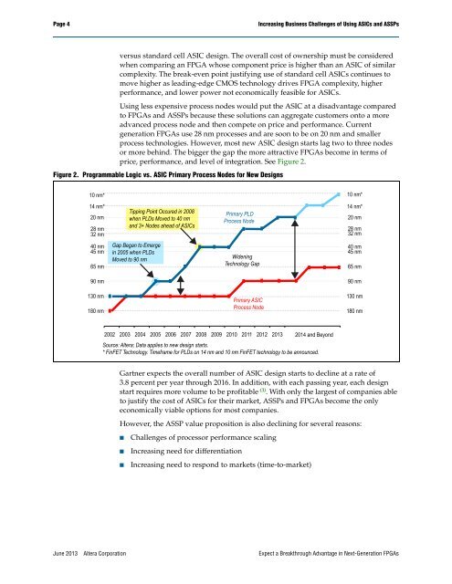
Us<strong>in</strong>g less expensive process nodes would put the ASIC at a disadvantage compared<br />
to <strong>FPGAs</strong> and ASSPs because these solutions can aggregate customers onto a more<br />
advanced process node and then compete on price and performance. Current<br />
generation <strong>FPGAs</strong> use 28 nm processes and are soon to be on 20 nm and smaller<br />
process technologies. However, most new ASIC design starts lag two to three nodes<br />
or more beh<strong>in</strong>d. The bigger the gap the more attractive <strong>FPGAs</strong> become <strong>in</strong> terms of<br />
price, performance, and level of <strong>in</strong>tegration. See Figure 2.<br />
Figure 2. Programmable Logic vs. ASIC Primary Process Nodes for New Designs<br />
10 nm*<br />
10 nm*<br />
14 nm*<br />
14 nm*<br />
Tipp<strong>in</strong>g Po<strong>in</strong>t Occured <strong>in</strong> 2008<br />
Primary PLD<br />
20 nm when PLDs Moved to 40 nm<br />
20 nm<br />
Process Node<br />
and 3+ Nodes ahead of ASICs<br />
28 nm<br />
28 nm<br />
32 nm 32 nm<br />
40 nm Gap Began to Emerge<br />
40 nm<br />
45 nm <strong>in</strong> 2005 when PLDs<br />
45 nm<br />
Moved to 90 nm<br />
Widen<strong>in</strong>g<br />
65 nm<br />
Technology Gap<br />
65 nm<br />
90 nm<br />
130 nm<br />
180 nm<br />
Primary ASIC<br />
Process Node<br />
90 nm<br />
130 nm<br />
180 nm<br />
2002 2003 2004 2005 2006 2007 2008 2009 2010 2011 2012 2013 2014 and Beyond<br />
Source: <strong>Altera</strong>; Data applies to new design starts.<br />
* F<strong>in</strong>FET Technology. Timeframe for PLDs on 14 nm and 10 nm F<strong>in</strong>FET technology to be announced.<br />
Gartner expects the overall number of ASIC design starts to decl<strong>in</strong>e at a rate of<br />
3.8 percent per year through 2016. In addition, with each pass<strong>in</strong>g year, each design<br />
start requires more volume to be profitable (3) . With only the largest of companies able<br />
to justify the cost of ASICs for their market, ASSPs and <strong>FPGAs</strong> become the only<br />
economically viable options for most companies.<br />
However, the ASSP value proposition is also decl<strong>in</strong><strong>in</strong>g for several reasons:<br />
■<br />
■<br />
■<br />
Challenges of processor performance scal<strong>in</strong>g<br />
Increas<strong>in</strong>g need for differentiation<br />
Increas<strong>in</strong>g need to respond to markets (time-to-market)<br />
June 2013 <strong>Altera</strong> Corporation <strong>Expect</strong> a <strong>Breakthrough</strong> <strong>Advantage</strong> <strong>in</strong> <strong>Next</strong>-<strong>Generation</strong> <strong>FPGAs</strong>


