

LM2587 SIMPLE SWITCHER 5A Flyback Regulator - Datasheet ...
LM2587 SIMPLE SWITCHER 5A Flyback Regulator - Datasheet ...
LM2587 SIMPLE SWITCHER 5A Flyback Regulator - Datasheet ...

You also want an ePaper? Increase the reach of your titles
YUMPU automatically turns print PDFs into web optimized ePapers that Google loves.
<strong>LM2587</strong><br />
<strong>SIMPLE</strong> <strong>SWITCHER</strong> <strong>5A</strong> <strong>Flyback</strong> <strong>Regulator</strong><br />
General Description<br />
The <strong>LM2587</strong> series of regulators are monolithic integrated<br />
circuits specifically designed for flyback step-up (boost)<br />
and forward converter applications The device is available<br />
in 4 different output voltage versions 33V 50V 12V and<br />
adjustable<br />
Requiring a minimum number of external components<br />
these regulators are cost effective and simple to use Included<br />
in the datasheet are typical circuits of boost and flyback<br />
regulators Also listed are selector guides for diodes<br />
and capacitors and a family of standard inductors and flyback<br />
transformers designed to work with these switching<br />
regulators<br />
The power switch is a 50A NPN device that can stand-off<br />
65V Protecting the power switch are current and thermal<br />
limiting circuits and an undervoltage lockout circuit This IC<br />
contains a 100 kHz fixed-frequency internal oscillator that<br />
permits the use of small magnetics Other features include<br />
soft start mode to reduce in-rush current during start up<br />
current mode control for improved rejection of input voltage<br />
and output load transients and cycle-by-cycle current limiting<br />
An output voltage tolerance of g4% within specified<br />
input voltages and output load conditions is guaranteed for<br />
the power supply system<br />
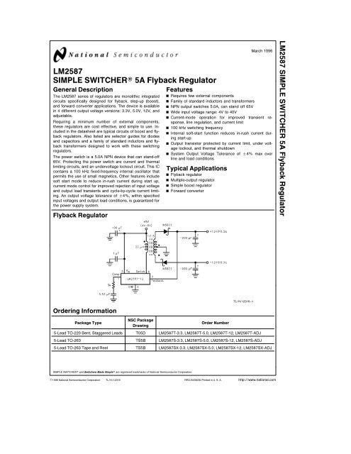
<strong>Flyback</strong> <strong>Regulator</strong><br />
Features<br />
March 1996<br />
Y Requires few external components<br />
Y Family of standard inductors and transformers<br />
Y NPN output switches 50A can stand off 65V<br />
Y Wide input voltage range 4V to 40V<br />
Y Current-mode operation for improved transient response<br />
line regulation and current limit<br />
Y 100 kHz switching frequency<br />
Y Internal soft-start function reduces in-rush current during<br />
start-up<br />
Y Output transistor protected by current limit under voltage<br />
lockout and thermal shutdown<br />
Y System Output Voltage Tolerance of g4% max over<br />
line and load conditions<br />
Typical Applications<br />
Y<br />
Y<br />
Y<br />
Y<br />
<strong>Flyback</strong> regulator<br />
Multiple-output regulator<br />
Simple boost regulator<br />
Forward converter<br />
<strong>LM2587</strong> <strong>SIMPLE</strong> <strong>SWITCHER</strong> <strong>5A</strong> <strong>Flyback</strong> <strong>Regulator</strong><br />
TLH12316–1<br />
Ordering Information<br />
Package Type<br />
NSC Package<br />
Drawing<br />
Order Number<br />
5-Lead TO-220 Bent Staggered Leads T05D <strong>LM2587</strong>T-33 <strong>LM2587</strong>T-50 <strong>LM2587</strong>T-12 <strong>LM2587</strong>T-ADJ<br />
5-Lead TO-263 TS5B <strong>LM2587</strong>S-33 <strong>LM2587</strong>S-50 <strong>LM2587</strong>S-12 <strong>LM2587</strong>S-ADJ<br />
5-Lead TO-263 Tape and Reel TS5B <strong>LM2587</strong>SX-33 <strong>LM2587</strong>SX-50 <strong>LM2587</strong>SX-12 <strong>LM2587</strong>SX-ADJ<br />
<strong>SIMPLE</strong> <strong>SWITCHER</strong> and Switchers Made Simple are registered trademarks of National Semiconductor Corporation<br />
C1996 National Semiconductor Corporation TLH12316<br />
RRD-B30M36Printed in U S A httpwwwnationalcom
Absolute Maximum Ratings (Note 1)<br />
If MilitaryAerospace specified devices are required<br />
please contact the National Semiconductor Sales<br />
OfficeDistributors for availability and specifications<br />
Input Voltage<br />
b04V s V IN<br />
s 45V<br />
Switch Voltage<br />
b04V s V SW<br />
s 65V<br />
Switch Current (Note 2)<br />
Internally Limited<br />
Compensation Pin Voltage b04V s V COMP<br />
s 24V<br />
Feedback Pin Voltage<br />
b04V s V FB<br />
s 2V OUT<br />
Power Dissipation (Note 3)<br />
Internally Limited<br />
Storage Temperature Range<br />
b65Ctoa150C<br />
Lead Temperature (Soldering 10 sec)<br />
260C<br />
Maximum Junction Temperature (Note 3)<br />
150C<br />
Minimum ESD Rating (C e 100 pF R e 15 kX 2kV<br />
Operating Ratings<br />
Supply Voltage<br />
Output Switch Voltage<br />
Output Switch Current<br />
Junction Temperature Range<br />
4V s V IN<br />
s 40V<br />
0V s V SW<br />
s 60V<br />
I SW<br />
s 50A<br />
b40C s T J<br />
s a125C<br />
Electrical Characteristics<br />
Specifications with standard type face are for T J e 25C and those in bold type face apply over full Operating Temperature<br />
Range Unless otherwise specified V IN e 5V<br />
<strong>LM2587</strong>-33<br />
Symbol Parameters Conditions Typical Min Max Units<br />
SYSTEM PARAMETERS Test Circuit of Figure 2 (Note 4)<br />
V OUT Output Voltage V IN e 4V to 12V<br />
I LOAD e 400 mA to 17<strong>5A</strong><br />
DV OUT Line Regulation V IN e 4V to 12V<br />
DV IN<br />
I LOAD e 400 mA<br />
DV OUT Load Regulation V IN e 12V<br />
DI LOAD<br />
I LOAD e 400 mA to 17<strong>5A</strong><br />
33 317314 343346 V<br />
20 50100 mV<br />
20 50100 mV<br />
h Efficiency V IN e 12V I LOAD e 1A 75 %<br />
UNIQUE DEVICE PARAMETERS (Note 5)<br />
V REF Output Reference Measured at Feedback Pin<br />
Voltage<br />
V COMP e 10V<br />
DV REF Reference Voltage V IN e 4V to 40V<br />
Line Regulation<br />
G M Error Amp I COMP eb30 mAtoa30 mA<br />
Transconductance V COMP e 10V<br />
A VOL Error Amp V COMP e 05V to 16V<br />
Voltage Gain R COMP e 10 MX (Note 6)<br />
<strong>LM2587</strong>-50<br />
33 32423234 33583366 V<br />
20<br />
mV<br />
1193 0678 2259 mmho<br />
260 15175 VV<br />
Symbol Parameters Conditions Typical Min Max Units<br />
SYSTEM PARAMETERS Test Circuit of Figure 2 (Note 4)<br />
V OUT Output Voltage V IN e 4V to 12V<br />
I LOAD e 500 mA to 14<strong>5A</strong><br />
DV OUT Line Regulation V IN e 4V to 12V<br />
DV IN<br />
I LOAD e 500 mA<br />
DV OUT Load Regulation V IN e 12V<br />
DI LOAD<br />
I LOAD e 500 mA to 14<strong>5A</strong><br />
50 480475 520525 V<br />
20 50100 mV<br />
20 50100 mV<br />
h Efficiency V IN e 12V I LOAD e 750 mA 80 %<br />
httpwwwnationalcom 2
Electrical Characteristics<br />
Specifications with standard type face are for T J e 25C and those in bold type face apply over full Operating Temperature<br />
Range Unless otherwise specified V IN e 5V (Continued)<br />
<strong>LM2587</strong>-50 (Continued)<br />
Symbol Parameters Conditions Typical Min Max Units<br />
UNIQUE DEVICE PARAMETERS (Note 5)<br />
V REF Output Reference Measured at Feedback Pin<br />
Voltage<br />
V COMP e 10V<br />
DV REF Reference Voltage V IN e 4V to 40V<br />
Line Regulation<br />
G M Error Amp I COMP eb30 mAtoa30 mA<br />
Transconductance V COMP e 10V<br />
A VOL Error Amp V COMP e 05V to 16V<br />
Voltage Gain R COMP e 10 MX (Note 6)<br />
<strong>LM2587</strong>-12<br />
50 49134900 50885100 V<br />
33<br />
mV<br />
0750 0447 1491 mmho<br />
165 9949 VV<br />
Symbol Parameters Conditions Typical Min Max Units<br />
SYSTEM PARAMETERS Test Circuit of Figure 3 (Note 4)<br />
V OUT Output Voltage V IN e 4V to 10V<br />
I LOAD e 300 mA to 12A<br />
DV OUT Line Regulation V IN e 4V to 10V<br />
DV IN<br />
I LOAD e 300 mA<br />
DV OUT Load Regulation V IN e 10V<br />
DI LOAD<br />
I LOAD e 300 mA to 12A<br />
120 11521140 12481260 V<br />
20 100200 mV<br />
20 100200 mV<br />
h Efficiency V IN e 10V I LOAD e 1A 90 %<br />
UNIQUE DEVICE PARAMETERS (Note 5)<br />
V REF Output Reference Measured at Feedback Pin<br />
Voltage<br />
V COMP e 10V<br />
DV REF Reference Voltage V IN e 4V to 40V<br />
Line Regulation<br />
G M Error Amp I COMP eb30 mAtoa30 mA<br />
Transconductance V COMP e 10V<br />
A VOL Error Amp V COMP e 05V to 16V<br />
Voltage Gain R COMP e 10 MX (Note 6)<br />
<strong>LM2587</strong>-ADJ<br />
120 11791176 12211224 V<br />
78<br />
mV<br />
0328 0186 0621 mmho<br />
70 4121 VV<br />
Symbol Parameters Conditions Typical Min Max Units<br />
SYSTEM PARAMETERS Test Circuit of Figure 3 (Note 4)<br />
V OUT Output Voltage V IN e 4V to 10V<br />
I LOAD e 300 mA to 12A<br />
DV OUT Line Regulation V IN e 4V to 10V<br />
DV IN<br />
I LOAD e 300 mA<br />
DV OUT Load Regulation V IN e 10V<br />
DI LOAD<br />
I LOAD e 300 mA to 12A<br />
120 11521140 12481260 V<br />
20 100200 mV<br />
20 100200 mV<br />
h Efficiency V IN e 10V I LOAD e 1A 90 %<br />
3<br />
httpwwwnationalcom
Electrical Characteristics<br />
Specifications with standard type face are for T J e 25C and those in bold type face apply over full Operating Temperature<br />
Range Unless otherwise specified V IN e 5V (Continued)<br />
<strong>LM2587</strong>-ADJ (Continued)<br />
Symbol Parameters Conditions Typical Min Max Units<br />
UNIQUE DEVICE PARAMETERS (Note 5)<br />
V REF Output Reference Measured at Feedback Pin<br />
Voltage<br />
V COMP e 10V<br />
DV REF Reference Voltage V IN e 4V to 40V<br />
Line Regulation<br />
G M Error Amp I COMP eb30 mAtoa30 mA<br />
Transconductance V COMP e 10V<br />
A VOL Error Amp V COMP e 05V to 16V<br />
Voltage Gain R COMP e 10 MX (Note 6)<br />
I B Error Amp V COMP e 10V<br />
Input Bias Current<br />
COMMON DEVICE PARAMETERS for all versions (Note 5)<br />
1230 12081205 12521255 V<br />
15<br />
mV<br />
3200 1800 6000 mmho<br />
670 400200 VV<br />
125 425600 nA<br />
Symbol Parameters Conditions Typical Min Max Units<br />
I S Input Supply Current (Switch Off)<br />
(Note 8)<br />
V UV Input Supply R LOAD e 100X<br />
Undervoltage Lockout<br />
11 155165 mA<br />
I SWITCH e 30A 85 140 165 mA<br />
330 305 375 V<br />
f O Oscillator Frequency Measured at Switch Pin<br />
R LOAD e 100X 100 8575 115125 kHz<br />
V COMP e 10V<br />
f SC Short-Circuit Measured at Switch Pin<br />
Frequency R LOAD e 100X 25 kHz<br />
V FEEDBACK e 115V<br />
V EAO Error Amplifier Upper Limit<br />
Output Swing (Note 7)<br />
28 2624 V<br />
Lower Limit<br />
(Note 8)<br />
025 040055 V<br />
I EAO Error Amp (Note 9)<br />
Output Current 165 11070 260320 mA<br />
(Source or Sink)<br />
I SS Soft Start Current V FEEDBACK e 092V<br />
V COMP e 10V<br />
110 8070 170190 mA<br />
D Maximum Duty Cycle R LOAD e 100X<br />
(Note 7)<br />
I L Switch Leakage Switch Off<br />
Current<br />
V SWITCH e 60V<br />
V SUS Switch Sustaining dVdT e 15Vns<br />
Voltage<br />
V SAT Switch Saturation I SWITCH e 50A<br />
Voltage<br />
I CL<br />
NPN Switch<br />
Current Limit<br />
98 9390 %<br />
15 300600 mA<br />
65 V<br />
07 1114 V<br />
65 50 95 A<br />
httpwwwnationalcom 4
Electrical Characteristics<br />
Specifications with standard type face are for T J e 25C and those in bold type face apply over full Operating Temperature<br />
Range Unless otherwise specified V IN e 5V (Continued)<br />
COMMON DEVICE PARAMETERS (Note 4) (Continued)<br />
Symbol Parameters Conditions Typical Min Max Units<br />
i JA Thermal Resistance T Package Junction to Ambient (Note 10) 65<br />
i JA T Package Junction to Ambient (Note 11) 45<br />
i JC T Package Junction to Case 2<br />
i JA S Package Junction to Ambient (Note 12) 56<br />
CW<br />
i JA S Package Junction to Ambient (Note 13) 35<br />
i JA S Package Junction to Ambient (Note 14) 26<br />
i JC S Package Junction to Case 2<br />
Note 1 Absolute Maximum Ratings indicate limits beyond which damage to the device may occur Operating ratings indicate conditions the device is intended to<br />
be functional but device parameter specifications may not be guaranteed under these conditions For guaranteed specifications and test conditions see the<br />
Electrical Characteristics<br />
Note 2 Note that switch current and output current are not identical in a step-up regulator Output current cannot be internally limited when the <strong>LM2587</strong> is used as<br />
a step-up regulator To prevent damage to the switch the output current must be externally limited to <strong>5A</strong> However output current is internally limited when the<br />
<strong>LM2587</strong> is used as a flyback regulator (see the Application Hints section for more information)<br />
Note 3 The junction temperature of the device (T J ) is a function of the ambient temperature (T A ) the junction-to-ambient thermal resistance (i JA ) and the power<br />
dissipation of the device (P D ) A thermal shutdown will occur if the temperature exceeds the maximum junction temperature of the device P D<br />
c i JA a T A(MAX)<br />
t<br />
T J(MAX) For a safe thermal design check that the maximum power dissipated by the device is less than P D<br />
s T J(MAX) b T A(MAX) )i JA When calculating the<br />
maximum allowable power dissipation derate the maximum junction temperaturethis ensures a margin of safety in the thermal design<br />
Note 4 External components such as the diode inductor input and output capacitors can affect switching regulator performance When the <strong>LM2587</strong> is used as<br />
shown in Figures 2 and 3 system performance will be as specified by the system parameters<br />
Note 5 All room temperature limits are 100% production tested and all limits at temperature extremes are guaranteed via correlation using standard Statistical<br />
Quality Control (SQC) methods<br />
Note 6 A 10 MX resistor is connected to the compensation pin (which is the error amplifier output) to ensure accuracy in measuring A VOL <br />
Note 7 To measure this parameter the feedback voltage is set to a low value depending on the output version of the device to force the error amplifier output<br />
high Adj V FB e 105V 33V V FB e 281V 50V V FB e 425V 12V V FB e 1020V<br />
Note 8 To measure this parameter the feedback voltage is set to a high value depending on the output version of the device to force the error amplifier output<br />
low Adj V FB e 141V 33V V FB e 380V 50V V FB e 575V 12V V FB e 1380V<br />
Note 9 To measure the worst-case error amplifier output current the <strong>LM2587</strong> is tested with the feedback voltage set to its low value (specified in Note 7) and at its<br />
high value (specified in Note 8)<br />
Note 10 Junction to ambient thermal resistance (no external heat sink) for the 5 lead TO-220 package mounted vertically with inch leads in a socket or on a<br />
PC board with minimum copper area<br />
Note 11 Junction to ambient thermal resistance (no external heat sink) for the 5 lead TO-220 package mounted vertically with inch leads soldered to a PC<br />
board containing approximately 4 square inches of (1oz) copper area surrounding the leads<br />
Note 12 Junction to ambient thermal resistance for the 5 lead TO-263 mounted horizontally against a PC board area of 0136 square inches (the same size as the<br />
TO-263 package) of 1 oz (00014 in thick) copper<br />
Note 13 Junction to ambient thermal resistance for the 5 lead TO-263 mounted horizontally against a PC board area of 04896 square inches (36 times the area of<br />
the TO-263 package) of 1 oz (00014 in thick) copper<br />
Note 14 Junction to ambient thermal resistance for the 5 lead TO-263 mounted horizontally against a PC board copper area of 10064 square inches (74 times the<br />
area of the TO-263 package) of 1 oz (00014 in thick) copper Additional copper area will reduce thermal resistance further See the thermal model in Switchers<br />
Made Simple software<br />
5<br />
httpwwwnationalcom
Typical Performance Characteristics<br />
Supply Current<br />
vs Temperature<br />
Reference Voltage<br />
vs Temperature<br />
DReference Voltage<br />
vs Supply Voltage<br />
Supply Current<br />
vs Switch Current<br />
Current Limit<br />
vs Temperature<br />
Feedback Pin Bias<br />
Current vs Temperature<br />
Switch Saturation<br />
Voltage vs Temperature<br />
Switch Transconductance<br />
vs Temperature<br />
Oscillator Frequency<br />
vs Temperature<br />
Error Amp Transconductance<br />
vs Temperature<br />
Error Amp Voltage<br />
Gain vs Temperature<br />
Short Circuit Frequency<br />
vs Temperature<br />
TLH12316–2<br />
httpwwwnationalcom 6
Connection Diagrams<br />
Bent Staggered Leads<br />
5-Lead TO-220 (T)<br />
Top View<br />
Bent Staggered Leads<br />
5-Lead TO-220 (T)<br />
Side View<br />
TLH12316–3<br />
Order Number <strong>LM2587</strong>T-33 <strong>LM2587</strong>T-50<br />
<strong>LM2587</strong>T-12 or <strong>LM2587</strong>T-ADJ<br />
See NS Package Number T05D<br />
TLH12316–4<br />
5-Lead TO-263 (S)<br />
Top View<br />
5-Lead TO-263 (S)<br />
Side View<br />
TLH12316–6<br />
Block Diagram<br />
TLH12316–5<br />
Order Number <strong>LM2587</strong>S-33 <strong>LM2587</strong>S-50<br />
<strong>LM2587</strong>S-12 or <strong>LM2587</strong>S-ADJ<br />
See NS Package Number TS5B<br />
For Fixed Versions<br />
33V R1 e 34k R2 e 2k<br />
5V R1 e 615k R2 e 2k<br />
12V R1 e 873k R2 e 1k<br />
For Adj Version<br />
R1 e Short (0X) R2 e Open<br />
FIGURE 1<br />
TLH12316–7<br />
7<br />
httpwwwnationalcom
Test Circuits<br />
C IN1 100 mF 25V Aluminum Electrolytic<br />
C IN2 01 mF Ceramic<br />
T22 mH 11 Schott 67141450<br />
D1N5820<br />
C OUT 680 mF 16V Aluminum Electrolytic<br />
C C 047 mF Ceramic<br />
R C 2k<br />
TLH12316–8<br />
FIGURE 2 <strong>LM2587</strong>-33 and <strong>LM2587</strong>-50<br />
C IN1 100 mF 25V Aluminum Electrolytic<br />
C IN2 01 mF Ceramic<br />
L15 mH Renco RL-5472-5<br />
D1N5820<br />
C OUT 680 mF 16V Aluminum Electrolytic<br />
C C 047 mF Ceramic<br />
R C 2k<br />
For 12V Devices R 1 e Short (0X) and R 2 e<br />
Open<br />
For ADJ Devices R 1 e 4875k g01% and R2<br />
e 562k g1%<br />
TLH12316–9<br />
FIGURE 3 <strong>LM2587</strong>-12 and <strong>LM2587</strong>-ADJ<br />
httpwwwnationalcom 8
<strong>Flyback</strong> <strong>Regulator</strong> Operation<br />
The <strong>LM2587</strong> is ideally suited for use in the flyback regulator<br />
topology The flyback regulator can produce a single output<br />
voltage such as the one shown in Figure 4 or multiple output<br />
voltages In Figure 4 the flyback regulator generates an<br />
output voltage that is inside the range of the input voltage<br />
This feature is unique to flyback regulators and cannot be<br />
duplicated with buck or boost regulators<br />
The operation of a flyback regulator is as follows (refer to<br />
Figure 4 ) when the switch is on current flows through the<br />
primary winding of the transformer T1 storing energy in the<br />
magnetic field of the transformer Note that the primary and<br />
secondary windings are out of phase so no current flows<br />
through the secondary when current flows through the primary<br />
When the switch turns off the magnetic field collapses<br />
reversing the voltage polarity of the primary and secondary<br />
windings Now rectifier D1 is forward biased and current<br />
flows through it releasing the energy stored in the<br />
transformer This produces voltage at the output<br />
The output voltage is controlled by modulating the peak<br />
switch current This is done by feeding back a portion of the<br />
output voltage to the error amp which amplifies the difference<br />
between the feedback voltage and a 1230V reference<br />
The error amp output voltage is compared to a ramp<br />
voltage proportional to the switch current (ie inductor current<br />
during the switch on time) The comparator terminates<br />
the switch on time when the two voltages are equal thereby<br />
controlling the peak switch current to maintain a constant<br />
output voltage<br />
TLH12316–10<br />
As shown in Figure 4 the <strong>LM2587</strong> can be used as a flyback regulator by using a minimum number of external components The switching waveforms of this<br />
regulator are shown in Figure 5 Typical Performance Characteristics observed during the operation of this circuit are shown in Figure 6<br />
FIGURE 4 12V <strong>Flyback</strong> <strong>Regulator</strong> Design Example<br />
9<br />
httpwwwnationalcom
Typical Performance Characteristics<br />
A Switch Voltage 10 Vdiv<br />
B Switch Current 5 Adiv<br />
C Output Rectifier Current 5 Adiv<br />
D Output Ripple Voltage 100 mVdiv<br />
AC-Coupled<br />
Horizontal 2 msdiv<br />
TLH12316–11<br />
FIGURE 5 Switching Waveforms<br />
FIGURE 6 V OUT Load Current Step Response<br />
TLH12316–12<br />
httpwwwnationalcom 10
Typical <strong>Flyback</strong> <strong>Regulator</strong> Applications<br />
Figures 7 through 12 show six typical flyback applications<br />
varying from single output to triple output Each drawing<br />
contains the part number(s) and manufacturer(s) for every<br />
component except the transformer For the transformer part<br />
numbers and manufacturers names see the table in<br />
Figure 13 For applications with different output voltages<br />
requiring the <strong>LM2587</strong>-ADJor different output configurations<br />
that do not match the standard configurations refer to<br />
the Switchers Made Simple software<br />
FIGURE 7 Single-Output <strong>Flyback</strong> <strong>Regulator</strong><br />
TLH12316–13<br />
FIGURE 8 Single-Output <strong>Flyback</strong> <strong>Regulator</strong><br />
TLH12316–14<br />
11<br />
httpwwwnationalcom
Typical <strong>Flyback</strong> <strong>Regulator</strong> Applications (Continued)<br />
FIGURE 9 Single-Output <strong>Flyback</strong> <strong>Regulator</strong><br />
TLH12316–15<br />
FIGURE 10 Dual-Output <strong>Flyback</strong> <strong>Regulator</strong><br />
TLH12316–16<br />
httpwwwnationalcom 12
Typical <strong>Flyback</strong> <strong>Regulator</strong> Applications (Continued)<br />
FIGURE 11 Dual-Output <strong>Flyback</strong> <strong>Regulator</strong><br />
TLH12316–17<br />
FIGURE 12 Triple-Output <strong>Flyback</strong> <strong>Regulator</strong><br />
TLH12316–18<br />
13<br />
httpwwwnationalcom
Typical <strong>Flyback</strong> <strong>Regulator</strong> Applications (Continued)<br />
Transformer Selection (T)<br />
Figure 13 lists the standard transformers available for flyback regulator applications Included in the table are the turns ratio(s)<br />
for each transformer as well as the output voltages input voltage ranges and the maximum load currents for each circuit<br />
Applications Figure 7 Figure 8 Figure 9 Figure 10 Figure 11 Figure 12<br />
Transformers T1 T1 T1 T2 T3 T4<br />
V IN 4V–6V 4V–6V 8V–16V 4V–6V 18V–36V 18V–36V<br />
V OUT1 33V 5V 12V 12V 12V 5V<br />
I OUT1 (Max) 18A 14A 12A 03A 1A 2<strong>5A</strong><br />
N 1 1 1 1 25 08 035<br />
V OUT2 b12V b12V 12V<br />
I OUT2 (Max) 03A 1A 0<strong>5A</strong><br />
N 2 25 08 08<br />
V OUT3<br />
b12V<br />
I OUT3 (Max)<br />
N 3<br />
FIGURE 13 Transformer Selection Table<br />
0<strong>5A</strong><br />
08<br />
Transformer<br />
Type<br />
Manufacturers’ Part Numbers<br />
Coilcraft 1 Coilcraft1 Pulse2<br />
Surface Mount Surface Mount<br />
Renco 3 Schott 4<br />
T1 Q4434-B Q4435-B PE-68411 RL-5530 67141450<br />
T2 Q4337-B Q4436-B PE-68412 RL-5531 67140860<br />
T3 Q4343-B PE-68421 RL-5534 67140920<br />
T4 Q4344-B PE-68422 RL-5535 67140930<br />
Note 1 Coilcraft Inc Phone (800) 322-2645<br />
1102 Silver Lake Road Cary IL 60013 Fax (708) 639-1469<br />
Note 2 Pulse Engineering Inc Phone (619) 674-8100<br />
12220 World Trade Drive San Diego CA 92128 Fax (619) 674-8262<br />
Note 3 Renco Electronics Inc Phone (800) 645-5828<br />
60 Jeffryn Blvd East Deer Park NY 11729 Fax (516) 586-5562<br />
Note 4 Schott Corp Phone (612) 475-1173<br />
1000 Parkers Lane Road Wayzata MN 55391 Fax (612) 475-1786<br />
FIGURE 14 Transformer Manufacturer Guide<br />
httpwwwnationalcom 14
Typical <strong>Flyback</strong> <strong>Regulator</strong> Applications (Continued)<br />
Transformer Footprints<br />
Figures 15 through 32 show the footprints of each transformer listed in Figure 14<br />
T1<br />
T2<br />
TLH12316–30<br />
Top View<br />
FIGURE 15 Coilcraft Q4434-B<br />
TLH12316–31<br />
Top View<br />
FIGURE 16 Coilcraft Q4337-B<br />
T3<br />
T4<br />
TLH12316–32<br />
Top View<br />
FIGURE 17 Coilcraft Q4343-B<br />
TLH12316–33<br />
Top View<br />
FIGURE 18 Coilcraft Q4344-B<br />
T1<br />
T2<br />
TLH12316–34<br />
Top View<br />
FIGURE 19 Coilcraft Q4435-B<br />
(Surface Mount)<br />
TLH12316–35<br />
Top View<br />
FIGURE 20 Coilcraft Q4436-B<br />
(Surface Mount)<br />
15<br />
httpwwwnationalcom
Typical <strong>Flyback</strong> <strong>Regulator</strong> Applications (Continued)<br />
T1<br />
T2<br />
TLH12316–36<br />
Top View<br />
FIGURE 21 Pulse PE-68411<br />
(Surface Mount)<br />
TLH12316–37<br />
Top View<br />
FIGURE 22 Pulse PE-68412<br />
(Surface Mount)<br />
T3<br />
T4<br />
TLH12316–38<br />
Top View<br />
FIGURE 23 Pulse PE-68421<br />
(Surface Mount)<br />
TLH12316–39<br />
Top View<br />
FIGURE 24 Pulse PE-68422<br />
(Surface Mount)<br />
T1<br />
T2<br />
TLH12316–40<br />
Top View<br />
FIGURE 25 Renco RL-5530<br />
TLH12316–41<br />
Top View<br />
FIGURE 26 Renco RL-5531<br />
httpwwwnationalcom 16
Typical <strong>Flyback</strong> <strong>Regulator</strong> Applications (Continued)<br />
T3<br />
T4<br />
TLH12316–46<br />
Top View<br />
FIGURE 27 Renco RL-5534<br />
TLH12316–42<br />
Top View<br />
FIGURE 28 Renco RL-5535<br />
T1<br />
T2<br />
TLH12316–43<br />
Top View<br />
FIGURE 29 Schott 67141450<br />
TLH12316–44<br />
Top View<br />
FIGURE 30 Schott 67140860<br />
T3<br />
T4<br />
TLH12316–45<br />
Top View<br />
FIGURE 31 Schott 67140920<br />
TLH12316–47<br />
Top View<br />
FIGURE 32 Schott 67140930<br />
17<br />
httpwwwnationalcom
Step-Up (Boost) <strong>Regulator</strong> Operation<br />
Figure 33 shows the <strong>LM2587</strong> used as a step-up (boost) regulator<br />
This is a switching regulator that produces an output<br />
voltage greater than the input supply voltage<br />
A brief explanation of how the <strong>LM2587</strong> Boost <strong>Regulator</strong><br />
works is as follows (refer to Figure 33 ) When the NPN<br />
switch turns on the inductor current ramps up at the rate of<br />
V IN L storing energy in the inductor When the switch turns<br />
off the lower end of the inductor flies above V IN discharging<br />
its current through diode (D) into the output capacitor<br />
(C OUT ) at a rate of (V OUT b V IN )L Thus energy stored in<br />
the inductor during the switch on time is transferred to the<br />
output during the switch off time The output voltage is controlled<br />
by adjusting the peak switch current as described in<br />
the flyback regulator section<br />
TLH12316–19<br />
By adding a small number of external components (as shown in Figure 33 ) the <strong>LM2587</strong> can be used to produce a regulated output voltage that is greater than the<br />
applied input voltage The switching waveforms observed during the operation of this circuit are shown in Figure 34 Typical performance of this regulator is shown<br />
in Figure 35<br />
FIGURE 33 12V Boost <strong>Regulator</strong><br />
Typical Performance Characteristics<br />
A Switch Voltage 10 Vdiv<br />
B Switch Current 5 Adiv<br />
C Inductor Current 5 Adiv<br />
D Output Ripple Voltage<br />
100 mVdiv AC-Coupled<br />
Horizontal 2 msdiv<br />
TLH12316–20<br />
FIGURE 34 Switching Waveforms<br />
FIGURE 35 V OUT Response to Load Current Step<br />
TLH12316–21<br />
httpwwwnationalcom 18
Typical Boost <strong>Regulator</strong> Applications<br />
Figures 36 and 38 through 40 show four typical boost applications)one<br />
fixed and three using the adjustable version<br />
of the <strong>LM2587</strong> Each drawing contains the part number(s)<br />
and manufacturer(s) for every component For the fixed 12V<br />
output application the part numbers and manufacturers’<br />
names for the inductor are listed in a table in Figure 40 For<br />
applications with different output voltages refer to the<br />
Switchers Made Simple software<br />
FIGURE 36 a5V to a12V Boost <strong>Regulator</strong><br />
TLH12316–22<br />
Figure 37 contains a table of standard inductors by part number and corresponding manufacturer for the fixed output regulator<br />
of Figure 36<br />
Coilcraft1 Pulse2 Renco3 Schott4<br />
R4793-A PE-53900 RL-5472-5 67146520<br />
Note 1 Coilcraft Inc Phone (800) 322-2645<br />
1102 Silver Lake Road Cary IL 60013 Fax (708) 639-1469<br />
Note 2 Pulse Engineering Inc Phone (619) 674-8100<br />
12220 World Trade Drive San Diego CA 92128 Fax (619) 674-8262<br />
Note 3 Renco Electronics Inc Phone (800) 645-5828<br />
60 Jeffryn Blvd East Deer Park NY 11729 Fax (516) 586-5562<br />
Note 4 Schott Corp Phone (612) 475-1173<br />
1000 Parkers Lane Road Wayzata MN 55391 Fax (612) 475-1786<br />
FIGURE 37 Inductor Selection Table<br />
19<br />
httpwwwnationalcom
Typical Boost <strong>Regulator</strong> Applications (Continued)<br />
FIGURE 38 a12V to a24V Boost <strong>Regulator</strong><br />
TLH12316–23<br />
FIGURE 39 a24V to a36V Boost <strong>Regulator</strong><br />
TLH12316–24<br />
FIGURE 40 a24V to a48V Boost <strong>Regulator</strong><br />
TLH12316–25<br />
The <strong>LM2587</strong> will require a heat sink in these applications The size of the heat sink will depend on the maximum ambient temperature To calculate the thermal<br />
resistance of the IC and the size of the heat sink needed see the ‘‘Heat SinkThermal Considerations’’ section in the Application Hints<br />
httpwwwnationalcom 20
Application Hints<br />
FIGURE 41 Boost <strong>Regulator</strong><br />
TLH12316–26<br />
PROGRAMMING OUTPUT VOLTAGE<br />
(SELECTING R 1 AND R 2 )<br />
Referring to the adjustable regulator in Figure 41 the output<br />
voltage is programmed by the resistors R 1 and R 2 by the<br />
following formula<br />
V OUT e V REF (1 a R 1 R 2 ) where V REF e 123V<br />
Resistors R 1 and R 2 divide the output voltage down so that<br />
it can be compared with the 123V internal reference With<br />
R 2 between 1k and 5k R 1 is<br />
R 1 e R 2 (V OUT V REF b 1) where V REF e 123V<br />
For best temperature coefficient and stability with time use<br />
1% metal film resistors<br />
SHORT CIRCUIT CONDITION<br />
Due to the inherent nature of boost regulators when the<br />
output is shorted (see Figure 41 ) current flows directly from<br />
the input through the inductor and the diode to the output<br />
bypassing the switch The current limit of the switch does<br />
not limit the output current for the entire circuit To protect<br />
the load and prevent damage to the switch the current must<br />
be externally limited either by the input supply or at the output<br />
with an external current limit circuit The external limit<br />
should be set to the maximum switch current of the device<br />
which is <strong>5A</strong><br />
In a flyback regulator application (Figure 42 ) using the standard<br />
transformers the <strong>LM2587</strong> will survive a short circuit to<br />
the main output When the output voltage drops to 80% of<br />
its nominal value the frequency will drop to 25 kHz With a<br />
lower frequency off times are larger With the longer off<br />
times the transformer can release all of its stored energy<br />
before the switch turns back on Hence the switch turns on<br />
initially with zero current at its collector In this condition the<br />
switch current limit will limit the peak current saving the<br />
device<br />
FLYBACK REGULATOR INPUT CAPACITORS<br />
A flyback regulator draws discontinuous pulses of current<br />
from the input supply Therefore there are two input capacitors<br />
needed in a flyback regulator one for energy storage<br />
and one for filtering (see Figure 42 ) Both are required due<br />
to the inherent operation of a flyback regulator To keep a<br />
stable or constant voltage supply to the <strong>LM2587</strong> a stor-<br />
FIGURE 42 <strong>Flyback</strong> <strong>Regulator</strong><br />
TLH12316–27<br />
21<br />
httpwwwnationalcom
Application Hints (Continued)<br />
age capacitor (t100 mF) is required If the input source is a<br />
recitified DC supply andor the application has a wide temperature<br />
range the required rms current rating of the capacitor<br />
might be very large This means a larger value of capacitance<br />
or a higher voltage rating will be needed of the input<br />
capacitor The storage capacitor will also attenuate noise<br />
which may interfere with other circuits connected to the<br />
same input supply voltage<br />
In addition a small bypass capacitor is required due to the<br />
noise generated by the input current pulses To eliminate<br />
the noise insert a 10 mF ceramic capacitor between V IN<br />
and ground as close as possible to the device<br />
SWITCH VOLTAGE LIMITS<br />
In a flyback regulator the maximum steady-state voltage<br />
appearing at the switch when it is off is set by the transformer<br />
turns ratio N the output voltage V OUT and the<br />
maximum input voltage V IN (Max)<br />
V SW(OFF) e V IN (Max) a (V OUT aV F )N<br />
where V F is the forward biased voltage of the output diode<br />
and is 05V for Schottky diodes and 08V for ultra-fast recovery<br />
diodes (typically) In certain circuits there exists a<br />
voltage spike V LL superimposed on top of the steady-state<br />
voltage (see Figure 5 waveform A) Usually this voltage<br />
spike is caused by the transformer leakage inductance and<br />
or the output rectifier recovery time To ‘‘clamp’’ the voltage<br />
at the switch from exceeding its maximum value a transient<br />
suppressor in series with a diode is inserted across the<br />
transformer primary (as shown in the circuit on the front<br />
page and other flyback regulator circuits throughout the datasheet)<br />
The schematic in Figure 42 shows another method<br />
of clamping the switch voltage A single voltage transient<br />
suppressor (the SA51A) is inserted at the switch pin This<br />
method clamps the total voltage across the switch not just<br />
the voltage across the primary<br />
If poor circuit layout techniques are used (see the ‘‘Circuit<br />
Layout Guideline’’ section) negative voltage transients may<br />
appear on the Switch pin (pin 4) Applying a negative voltage<br />
(with respect to the IC’s ground) to any monolithic IC<br />
pin causes erratic and unpredictable operation of that IC<br />
This holds true for the <strong>LM2587</strong> IC as well When used in a<br />
flyback regulator the voltage at the Switch pin (pin 4) can<br />
go negative when the switch turns on The ‘‘ringing’’ voltage<br />
at the switch pin is caused by the output diode capacitance<br />
and the transformer leakage inductance forming a resonant<br />
circuit at the secondary(ies) The resonant circuit generates<br />
the ‘‘ringing’’ voltage which gets reflected back through the<br />
transformer to the switch pin There are two common methods<br />
to avoid this problem One is to add an RC snubber<br />
around the output rectifier(s) as in Figure 42 The values of<br />
the resistor and the capacitor must be chosen so that the<br />
voltage at the Switch pin does not drop below b04V The<br />
resistor may range in value between 10X and1kX and the<br />
capacitor will vary from 0001 mF to01mF Adding a snubber<br />
will (slightly) reduce the efficiency of the overall circuit<br />
The other method to reduce or eliminate the ‘‘ringing’’ is to<br />
insert a Schottky diode clamp between pins 4 and 3<br />
(ground) also shown in Figure 42 This prevents the voltage<br />
at pin 4 from dropping below b04V The reverse voltage<br />
rating of the diode must be greater than the switch off voltage<br />
TLH12316–28<br />
FIGURE 43 Input Line Filter<br />
OUTPUT VOLTAGE LIMITATIONS<br />
The maximum output voltage of a boost regulator is the<br />
maximum switch voltage minus a diode drop In a flyback<br />
regulator the maximum output voltage is determined by the<br />
turns ratio N and the duty cycle D by the equation<br />
V OUT N c V IN<br />
c D(1 b D)<br />
The duty cycle of a flyback regulator is determined by the<br />
following equation<br />
V<br />
D e<br />
OUT a V F<br />
V<br />
OUT<br />
N(V IN b V SAT ) a V OUT a V F N(V IN ) a V OUT<br />
Theoretically the maximum output voltage can be as large<br />
as desiredjust keep increasing the turns ratio of the transformer<br />
However there exists some physical limitations that<br />
prevent the turns ratio and thus the output voltage from<br />
increasing to infinity The physical limitations are capacitances<br />
and inductances in the <strong>LM2587</strong> switch the output<br />
diode(s) and the transformersuch as reverse recovery<br />
time of the output diode (mentioned above)<br />
NOISY INPUT LINE CONDITION)<br />
A small low-pass RC filter should be used at the input pin of<br />
the <strong>LM2587</strong> if the input voltage has an unusual large<br />
amount of transient noise such as with an input switch that<br />
bounces The circuit in Figure 43 demonstrates the layout of<br />
the filter with the capacitor placed from the input pin to<br />
ground and the resistor placed between the input supply<br />
and the input pin Note that the values of R IN and C IN<br />
shown in the schematic are good enough for most applications<br />
but some readjusting might be required for a particular<br />
application If efficiency is a major concern replace the resistor<br />
with a small inductor (say 10 mH and rated at<br />
100 mA)<br />
STABILITY<br />
All current-mode controlled regulators can suffer from an<br />
instability known as subharmonic oscillation if they operate<br />
with a duty cycle above 50% To eliminate subharmonic oscillations<br />
a minimum value of inductance is required to ensure<br />
stability for all boost and flyback regulators The minimum<br />
inductance is given by<br />
L(Min) e 292 (V IN(Min) b V SAT ) c (2D(Max) b1)<br />
(mH)<br />
1 b D(Max)<br />
where V SAT is the switch saturation voltage and can be<br />
found in the Characteristic Curves<br />
httpwwwnationalcom 22
Application Hints (Continued)<br />
FIGURE 44 Circuit Board Layout<br />
TLH12316–29<br />
CIRCUIT LAYOUT GUIDELINES<br />
As in any switching regulator layout is very important Rapidly<br />
switching currents associated with wiring inductance<br />
generate voltage transients which can cause problems For<br />
minimal inductance and ground loops keep the length of<br />
the leads and traces as short as possible Use single point<br />
grounding or ground plane construction for best results<br />
Separate the signal grounds from the power grounds (as<br />
indicated in Figure 44 ) When using the Adjustable version<br />
physically locate the programming resistors as near the regulator<br />
IC as possible to keep the sensitive feedback wiring<br />
short<br />
HEAT SINKTHERMAL CONSIDERATIONS<br />
In many cases no heat sink is required to keep the <strong>LM2587</strong><br />
junction temperature within the allowed operating range For<br />
each application to determine whether or not a heat sink<br />
will be required the following must be identified<br />
1) Maximum ambient temperature (in the application)<br />
2) Maximum regulator power dissipation (in the application)<br />
3) Maximum allowed junction temperature (125C for the<br />
<strong>LM2587</strong>) For a safe conservative design a temperature<br />
approximately 15C cooler than the maximum junction temperature<br />
should be selected (110C)<br />
4) <strong>LM2587</strong> package thermal resistances i JA and i JC (given<br />
in the Electrical Characteristics)<br />
Total power dissipated (P D ) by the <strong>LM2587</strong> can be estimated<br />
as follows<br />
Boost<br />
P D e 015X c<br />
I LOAD<br />
1bD J 2 c D a<br />
I LOAD<br />
50c(1bD) c D c V IN<br />
<strong>Flyback</strong><br />
P D e 015X c<br />
N c RI LOAD<br />
1bD<br />
a NcRI LOAD<br />
50c(1bD) c D c V IN<br />
J 2 c D<br />
V IN is the minimum input voltage V OUT is the output voltage<br />
N is the transformer turns ratio D is the duty cycle and<br />
I LOAD is the maximum load current (and RI LOAD is the sum<br />
of the maximum load currents for multiple-output flyback<br />
regulators) The duty cycle is given by<br />
Boost<br />
D e<br />
V OUT a V F b V IN V OUT b V IN<br />
V OUT a V F b V SAT V OUT<br />
<strong>Flyback</strong><br />
V<br />
D e<br />
OUT a V F<br />
V<br />
OUT<br />
N(V IN b V SAT ) a V OUT a V F N(V IN ) a V OUT<br />
where V F is the forward biased voltage of the diode and is<br />
typically 05V for Schottky diodes and 08V for fast recovery<br />
diodes V SAT is the switch saturation voltage and can be<br />
found in the Characteristic Curves<br />
When no heat sink is used the junction temperature rise is<br />
DT J e P D<br />
c i JA <br />
Adding the junction temperature rise to the maximum ambient<br />
temperature gives the actual operating junction temperature<br />
T J e DT J a T A <br />
If the operating junction temperature exceeds the maximum<br />
junction temperatue in item 3 above then a heat sink is<br />
required When using a heat sink the junction temperature<br />
rise can be determined by the following<br />
DT J e P D<br />
c (i JC a i Interface a i Heat Sink )<br />
Again the operating junction temperature will be<br />
T J e DT J a T A<br />
23<br />
httpwwwnationalcom
Application Hints (Continued)<br />
As before if the maximum junction temperature is exceeded<br />
a larger heat sink is required (one that has a lower thermal<br />
resistance)<br />
Included in the Switchers Made Simple design software<br />
is a more precise (non-linear) thermal model that can be<br />
used to determine junction temperature with different inputoutput<br />
parameters or different component values It can<br />
also calculate the heat sink thermal resistance required to<br />
maintain the regulator junction temperature below the maximum<br />
operating temperature<br />
To further simplify the flyback regulator design procedure<br />
National Semiconductor is making available computer design<br />
software Switchers Made Simple software is available<br />
on a (3) diskette for IBM compatable computers<br />
from a National Semiconductor sales office in your area or<br />
the National Semiconductor Customer Response Center<br />
(1-800-272-9959)<br />
European Magnetic Vendor<br />
Contacts<br />
Please contact the following addresses for details of local<br />
distributors or representatives<br />
Coilcraft<br />
21 Napier Place<br />
Wardpark North<br />
Cumbernauld Scotland G68 0LL<br />
Phone a44 1236 730 595<br />
Fax a44 1236 730 627<br />
Pulse Engineering<br />
Dunmore Road<br />
Tuam<br />
Co Galway Ireland<br />
Phone a353 93 24 107<br />
Fax a353 93 24 459<br />
httpwwwnationalcom 24
Physical Dimensions inches (millimeters)<br />
Order Number <strong>LM2587</strong>T-33 <strong>LM2587</strong>T-50<br />
<strong>LM2587</strong>T-12 or <strong>LM2587</strong>T-ADJ<br />
NS Package Number T05D<br />
25<br />
httpwwwnationalcom
<strong>LM2587</strong> <strong>SIMPLE</strong> <strong>SWITCHER</strong> <strong>5A</strong> <strong>Flyback</strong> <strong>Regulator</strong><br />
Physical Dimensions inches (millimeters) (Continued)<br />
Order Number <strong>LM2587</strong>S-33 <strong>LM2587</strong>S-50<br />
<strong>LM2587</strong>S-12 or <strong>LM2587</strong>S-ADJ<br />
NS Package Number TS5B<br />
LIFE SUPPORT POLICY<br />
NATIONAL’S PRODUCTS ARE NOT AUTHORIZED FOR USE AS CRITICAL COMPONENTS IN LIFE SUPPORT<br />
DEVICES OR SYSTEMS WITHOUT THE EXPRESS WRITTEN APPROVAL OF THE PRESIDENT OF NATIONAL<br />
SEMICONDUCTOR CORPORATION As used herein<br />
1 Life support devices or systems are devices or 2 A critical component is any component of a life<br />
systems which (a) are intended for surgical implant support device or system whose failure to perform can<br />
into the body or (b) support or sustain life and whose be reasonably expected to cause the failure of the life<br />
failure to perform when properly used in accordance support device or system or to affect its safety or<br />
with instructions for use provided in the labeling can effectiveness<br />
be reasonably expected to result in a significant injury<br />
to the user<br />
National Semiconductor National Semiconductor National Semiconductor National Semiconductor<br />
Corporation Europe Hong Kong Ltd Japan Ltd<br />
1111 West Bardin Road Fax a49 (0) 180-530 85 86 13th Floor Straight Block Tel 81-043-299-2308<br />
Arlington TX 76017 Email europesupport nsccom Ocean Centre 5 Canton Rd Fax 81-043-299-2408<br />
Tel 1(800) 272-9959 Deutsch Tel a49 (0) 180-530 85 85 Tsimshatsui Kowloon<br />
Fax 1(800) 737-7018 English Tel a49 (0) 180-532 78 32 Hong Kong<br />
Franais Tel a49 (0) 180-532 93 58 Tel (852) 2737-1600<br />
httpwwwnationalcom Italiano Tel a49 (0) 180-534 16 80 Fax (852) 2736-9960<br />
National does not assume any responsibility for use of any circuitry described no circuit patent licenses are implied and National reserves the right at any time without notice to change said circuitry and specifications
This datasheet has been download from:<br />
www.datasheetcatalog.com<br />
<strong>Datasheet</strong>s for electronics components.


