


You also want an ePaper? Increase the reach of your titles
YUMPU automatically turns print PDFs into web optimized ePapers that Google loves.
<strong>VS1011e</strong><br />
VS1011E<br />
<strong>VS1011e</strong> - <strong>MPEG</strong> <strong>AUDIO</strong> <strong>CODEC</strong><br />
Features<br />
• Decodes <strong>MPEG</strong> 1.0 & 2.0 audio layer III<br />
(CBR, VBR, ABR); layers I & II optional;<br />
WAV (PCM + IMA ADPCM)<br />
• 320 kbit/s MP3 with 12.0 MHz external clock<br />
• Streaming support for MP1/2/3 and WAV<br />
• Bass and treble controls<br />
• Operates with single 12..13 MHz or 24..26<br />
MHz external clock<br />
• Internal clock doubler<br />
• Low-power operation<br />
• High-quality stereo DAC with no phase error<br />
between channels<br />
• Stereo earphone driver capable of driving a<br />
30Ω load<br />
• Separate 2.5 .. 3.6 V operating voltages for<br />
analog and digital<br />
• Serial control and data interfaces<br />
• Can be used as a slave co-processor<br />
• 5.5 KiB On-chip RAM for user code / data<br />
• SPI flash boot for special applications<br />
• New functions may be added with software<br />
and 4 GPIO pins<br />
• Lead-free and RoHS-compliant packages<br />
LPQFP-48 and BGA-49<br />
Description<br />
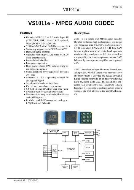
<strong>VS1011e</strong> is a single-chip <strong>MPEG</strong> audio decoder.<br />
The chip contains a high-performance, low-power<br />
DSP processor core VS DSP 4 , working memory,<br />
5 KiB instruction RAM and 0.5 KiB data RAM<br />
for user applications, serial control and input data<br />
interfaces, 4 general purpose I/O pins, as well as<br />
a high-quality variable-sample-rate stereo DAC,<br />
followed by an earphone amplifier and a ground<br />
buffer.<br />
<strong>VS1011e</strong> receives its input bitstream through a serial<br />
input bus, which it listens to as a system slave.<br />
The input stream is decoded and passed through a<br />
digital volume control to an 18-bit oversampling,<br />
multi-bit, sigma-delta DAC. The decoding is controlled<br />
via a serial control bus. In addition to basic<br />
decoding, it is possible to add application specific<br />
features, like DSP effects, to the user RAM memory.<br />
GPIO<br />
VS1011<br />
4<br />
GPIO<br />
Stereo<br />
DAC<br />
Stereo Ear−<br />
phone Driver<br />
audio<br />
L<br />
R<br />
output<br />
X ROM<br />
DREQ<br />
SO<br />
SI<br />
SCLK<br />
XCS<br />
XDCS<br />
Serial<br />
Data/<br />
Control<br />
Interface<br />
VSDSP 4<br />
X RAM<br />
Y ROM<br />
Y RAM<br />
Instruction<br />
RAM<br />
Instruction<br />
ROM<br />
Version 1.03, 2005-09-05 1
VLSI<br />
Solution y<br />
<strong>VS1011e</strong><br />
VS1011E<br />
CONTENTS<br />
Contents<br />
1 License 8<br />
2 Disclaimer 8<br />
3 Definitions 8<br />
4 Characteristics & Specifications 9<br />
4.1 Absolute Maximum Ratings . . . . . . . . . . . . . . . . . . . . . . . . . . . . . . . . 9<br />
4.2 Recommended Operating Conditions . . . . . . . . . . . . . . . . . . . . . . . . . . . . 9<br />
4.3 Analog Characteristics . . . . . . . . . . . . . . . . . . . . . . . . . . . . . . . . . . . 10<br />
4.4 Power Consumption . . . . . . . . . . . . . . . . . . . . . . . . . . . . . . . . . . . . . 10<br />
4.5 Digital Characteristics . . . . . . . . . . . . . . . . . . . . . . . . . . . . . . . . . . . 11<br />
4.6 Switching Characteristics - Boot Initialization . . . . . . . . . . . . . . . . . . . . . . . 11<br />
5 Packages and Pin Descriptions 12<br />
5.1 Packages . . . . . . . . . . . . . . . . . . . . . . . . . . . . . . . . . . . . . . . . . . 12<br />
5.1.1 LQFP-48 . . . . . . . . . . . . . . . . . . . . . . . . . . . . . . . . . . . . . . 12<br />
5.1.2 BGA-49 . . . . . . . . . . . . . . . . . . . . . . . . . . . . . . . . . . . . . . . 13<br />
5.1.3 SOIC-28 . . . . . . . . . . . . . . . . . . . . . . . . . . . . . . . . . . . . . . 13<br />
5.2 Pin Descriptions . . . . . . . . . . . . . . . . . . . . . . . . . . . . . . . . . . . . . . . 14<br />
5.2.1 LQFP-48 and BGA-49 Pin Descriptions . . . . . . . . . . . . . . . . . . . . . . 14<br />
5.2.2 SOIC-28 Pin Descriptions . . . . . . . . . . . . . . . . . . . . . . . . . . . . . 15<br />
6 Connection Diagram, LQFP-48 16<br />
7 SPI Buses 17<br />
Version 1.03, 2005-09-05 2
VLSI<br />
Solution y<br />
<strong>VS1011e</strong><br />
VS1011E<br />
CONTENTS<br />
7.1 General . . . . . . . . . . . . . . . . . . . . . . . . . . . . . . . . . . . . . . . . . . . 17<br />
7.2 SPI Bus Pin Descriptions . . . . . . . . . . . . . . . . . . . . . . . . . . . . . . . . . . 17<br />
7.2.1 VS1002 Native Modes (New Mode) . . . . . . . . . . . . . . . . . . . . . . . . 17<br />
7.2.2 VS1001 Compatibility Mode . . . . . . . . . . . . . . . . . . . . . . . . . . . . 17<br />
7.3 Serial Protocol for Serial Data Interface (SDI) . . . . . . . . . . . . . . . . . . . . . . . 18<br />
7.3.1 General . . . . . . . . . . . . . . . . . . . . . . . . . . . . . . . . . . . . . . . 18<br />
7.3.2 SDI in VS1002 Native Modes (New Mode) . . . . . . . . . . . . . . . . . . . . 18<br />
7.3.3 SDI in VS1001 Compatibility Mode . . . . . . . . . . . . . . . . . . . . . . . . 18<br />
7.4 Data Request Pin DREQ . . . . . . . . . . . . . . . . . . . . . . . . . . . . . . . . . . 19<br />
7.5 Serial Protocol for Serial Command Interface (SCI) . . . . . . . . . . . . . . . . . . . . 19<br />
7.5.1 General . . . . . . . . . . . . . . . . . . . . . . . . . . . . . . . . . . . . . . . 19<br />
7.5.2 SCI Read . . . . . . . . . . . . . . . . . . . . . . . . . . . . . . . . . . . . . . 20<br />
7.5.3 SCI Write . . . . . . . . . . . . . . . . . . . . . . . . . . . . . . . . . . . . . . 20<br />
7.6 SPI Timing Diagram . . . . . . . . . . . . . . . . . . . . . . . . . . . . . . . . . . . . 21<br />
7.7 SPI Examples with SM SDINEW and SM SDISHARED set . . . . . . . . . . . . . . . 22<br />
7.7.1 Two SCI Writes . . . . . . . . . . . . . . . . . . . . . . . . . . . . . . . . . . . 22<br />
7.7.2 Two SDI Bytes . . . . . . . . . . . . . . . . . . . . . . . . . . . . . . . . . . . 22<br />
7.7.3 SCI Operation in Middle of Two SDI Bytes . . . . . . . . . . . . . . . . . . . . 23<br />
8 Functional Description 24<br />
8.1 Main Features . . . . . . . . . . . . . . . . . . . . . . . . . . . . . . . . . . . . . . . . 24<br />
8.2 Supported Audio Codecs . . . . . . . . . . . . . . . . . . . . . . . . . . . . . . . . . . 24<br />
8.2.1 Supported MP1 (<strong>MPEG</strong> layer I) Formats . . . . . . . . . . . . . . . . . . . . . 24<br />
8.2.2 Supported MP2 (<strong>MPEG</strong> layer II) Formats . . . . . . . . . . . . . . . . . . . . . 25<br />
8.2.3 Supported MP3 (<strong>MPEG</strong> layer III) Formats . . . . . . . . . . . . . . . . . . . . 25<br />
Version 1.03, 2005-09-05 3
VLSI<br />
Solution y<br />
<strong>VS1011e</strong><br />
VS1011E<br />
CONTENTS<br />
8.2.4 Supported RIFF WAV Formats . . . . . . . . . . . . . . . . . . . . . . . . . . . 26<br />
8.3 Data Flow of <strong>VS1011e</strong> . . . . . . . . . . . . . . . . . . . . . . . . . . . . . . . . . . . 27<br />
8.4 Serial Data Interface (SDI) . . . . . . . . . . . . . . . . . . . . . . . . . . . . . . . . . 27<br />
8.5 Serial Control Interface (SCI) . . . . . . . . . . . . . . . . . . . . . . . . . . . . . . . . 28<br />
8.6 SCI Registers . . . . . . . . . . . . . . . . . . . . . . . . . . . . . . . . . . . . . . . . 28<br />
8.6.1 SCI MODE (RW) . . . . . . . . . . . . . . . . . . . . . . . . . . . . . . . . . 29<br />
8.6.2 SCI STATUS (RW) . . . . . . . . . . . . . . . . . . . . . . . . . . . . . . . . . 30<br />
8.6.3 SCI BASS (RW) . . . . . . . . . . . . . . . . . . . . . . . . . . . . . . . . . . 31<br />
8.6.4 SCI CLOCKF (RW) . . . . . . . . . . . . . . . . . . . . . . . . . . . . . . . . 31<br />
8.6.5 SCI DECODE TIME (RW) . . . . . . . . . . . . . . . . . . . . . . . . . . . . 32<br />
8.6.6 SCI AUDATA (RW) . . . . . . . . . . . . . . . . . . . . . . . . . . . . . . . . 32<br />
8.6.7 SCI WRAM (RW) . . . . . . . . . . . . . . . . . . . . . . . . . . . . . . . . . 32<br />
8.6.8 SCI WRAMADDR (RW) . . . . . . . . . . . . . . . . . . . . . . . . . . . . . 32<br />
8.6.9 SCI HDAT0 and SCI HDAT1 (R) . . . . . . . . . . . . . . . . . . . . . . . . . 33<br />
8.6.10 SCI AIADDR (RW) . . . . . . . . . . . . . . . . . . . . . . . . . . . . . . . . 34<br />
8.6.11 SCI VOL (RW) . . . . . . . . . . . . . . . . . . . . . . . . . . . . . . . . . . . 34<br />
8.6.12 SCI AICTRL[x] (RW) . . . . . . . . . . . . . . . . . . . . . . . . . . . . . . . 34<br />
9 Operation 35<br />
9.1 Clocking . . . . . . . . . . . . . . . . . . . . . . . . . . . . . . . . . . . . . . . . . . . 35<br />
9.2 Hardware Reset . . . . . . . . . . . . . . . . . . . . . . . . . . . . . . . . . . . . . . . 35<br />
9.3 Software Reset . . . . . . . . . . . . . . . . . . . . . . . . . . . . . . . . . . . . . . . 35<br />
9.4 SPI Boot . . . . . . . . . . . . . . . . . . . . . . . . . . . . . . . . . . . . . . . . . . . 36<br />
9.5 Play/Decode . . . . . . . . . . . . . . . . . . . . . . . . . . . . . . . . . . . . . . . . . 36<br />
9.6 Feeding PCM data . . . . . . . . . . . . . . . . . . . . . . . . . . . . . . . . . . . . . 36<br />
Version 1.03, 2005-09-05 4
VLSI<br />
Solution y<br />
<strong>VS1011e</strong><br />
VS1011E<br />
CONTENTS<br />
9.7 SDI Tests . . . . . . . . . . . . . . . . . . . . . . . . . . . . . . . . . . . . . . . . . . 36<br />
9.7.1 Sine Test . . . . . . . . . . . . . . . . . . . . . . . . . . . . . . . . . . . . . . 37<br />
9.7.2 Pin Test . . . . . . . . . . . . . . . . . . . . . . . . . . . . . . . . . . . . . . . 37<br />
9.7.3 Memory Test . . . . . . . . . . . . . . . . . . . . . . . . . . . . . . . . . . . . 37<br />
9.7.4 SCI Test . . . . . . . . . . . . . . . . . . . . . . . . . . . . . . . . . . . . . . . 38<br />
10 <strong>VS1011e</strong> Registers 39<br />
10.1 Who Needs to Read This Chapter . . . . . . . . . . . . . . . . . . . . . . . . . . . . . 39<br />
10.2 The Processor Core . . . . . . . . . . . . . . . . . . . . . . . . . . . . . . . . . . . . . 39<br />
10.3 <strong>VS1011e</strong> Memory Map . . . . . . . . . . . . . . . . . . . . . . . . . . . . . . . . . . . 39<br />
10.4 SCI Registers . . . . . . . . . . . . . . . . . . . . . . . . . . . . . . . . . . . . . . . . 39<br />
10.5 Serial Data Registers . . . . . . . . . . . . . . . . . . . . . . . . . . . . . . . . . . . . 40<br />
10.6 DAC Registers . . . . . . . . . . . . . . . . . . . . . . . . . . . . . . . . . . . . . . . 41<br />
10.7 GPIO Registers . . . . . . . . . . . . . . . . . . . . . . . . . . . . . . . . . . . . . . . 41<br />
10.8 Interrupt Registers . . . . . . . . . . . . . . . . . . . . . . . . . . . . . . . . . . . . . 42<br />
10.9 System Vector Tags . . . . . . . . . . . . . . . . . . . . . . . . . . . . . . . . . . . . . 43<br />
10.9.1 AudioInt, 0x20 . . . . . . . . . . . . . . . . . . . . . . . . . . . . . . . . . . . 43<br />
10.9.2 SciInt, 0x21 . . . . . . . . . . . . . . . . . . . . . . . . . . . . . . . . . . . . . 43<br />
10.9.3 DataInt, 0x22 . . . . . . . . . . . . . . . . . . . . . . . . . . . . . . . . . . . . 43<br />
10.9.4 UserCodec, 0x0 . . . . . . . . . . . . . . . . . . . . . . . . . . . . . . . . . . . 43<br />
10.10System Vector Functions . . . . . . . . . . . . . . . . . . . . . . . . . . . . . . . . . . 44<br />
10.10.1 WriteIRam(), 0x2 . . . . . . . . . . . . . . . . . . . . . . . . . . . . . . . . . . 44<br />
10.10.2 ReadIRam(), 0x4 . . . . . . . . . . . . . . . . . . . . . . . . . . . . . . . . . . 44<br />
10.10.3 DataBytes(), 0x6 . . . . . . . . . . . . . . . . . . . . . . . . . . . . . . . . . . 44<br />
10.10.4 GetDataByte(), 0x8 . . . . . . . . . . . . . . . . . . . . . . . . . . . . . . . . . 45<br />
Version 1.03, 2005-09-05 5
VLSI<br />
Solution y<br />
<strong>VS1011e</strong><br />
VS1011E<br />
CONTENTS<br />
10.10.5 GetDataWords(), 0xa . . . . . . . . . . . . . . . . . . . . . . . . . . . . . . . . 45<br />
11 VS1011 Version Changes 46<br />
11.1 Changes Between VS1011b and <strong>VS1011e</strong>, 2005-07-13 . . . . . . . . . . . . . . . . . . 46<br />
11.2 Migration Checklist from VS1011b to <strong>VS1011e</strong>, 2005-07-13 . . . . . . . . . . . . . . . 46<br />
12 Document Version Changes 47<br />
12.1 Version 1.03 for <strong>VS1011e</strong>, 2005-09-05 . . . . . . . . . . . . . . . . . . . . . . . . . . . 47<br />
12.2 Version 1.02 for <strong>VS1011e</strong>, 2005-07-13 . . . . . . . . . . . . . . . . . . . . . . . . . . . 47<br />
12.3 Version 1.01 for VS1011b, 2004-11-19 . . . . . . . . . . . . . . . . . . . . . . . . . . . 47<br />
12.4 Version 1.00 for VS1011b, 2004-10-22 . . . . . . . . . . . . . . . . . . . . . . . . . . . 47<br />
12.5 Version 0.71 for VS1011, 2004-07-20 . . . . . . . . . . . . . . . . . . . . . . . . . . . 47<br />
12.6 Version 0.70 for VS1011, 2004-05-13 . . . . . . . . . . . . . . . . . . . . . . . . . . . 47<br />
12.7 Version 0.62 for VS1011, 2004-03-24 . . . . . . . . . . . . . . . . . . . . . . . . . . . 47<br />
12.8 Version 0.61 for VS1011, 2004-03-11 . . . . . . . . . . . . . . . . . . . . . . . . . . . 47<br />
13 Contact Information 48<br />
Version 1.03, 2005-09-05 6
VLSI<br />
Solution y<br />
<strong>VS1011e</strong><br />
VS1011E<br />
LIST OF FIGURES<br />
List of Figures<br />
1 Pin Configuration, LQFP-48. . . . . . . . . . . . . . . . . . . . . . . . . . . . . . . . . 12<br />
2 Pin Configuration, BGA-49. . . . . . . . . . . . . . . . . . . . . . . . . . . . . . . . . 13<br />
3 Pin Configuration, SOIC-28. . . . . . . . . . . . . . . . . . . . . . . . . . . . . . . . . 13<br />
4 Typical Connection Diagram Using LQFP-48. . . . . . . . . . . . . . . . . . . . . . . . 16<br />
5 BSYNC Signal - one byte transfer. . . . . . . . . . . . . . . . . . . . . . . . . . . . . . 18<br />
6 BSYNC Signal - two byte transfer. . . . . . . . . . . . . . . . . . . . . . . . . . . . . . 18<br />
7 SCI Word Read . . . . . . . . . . . . . . . . . . . . . . . . . . . . . . . . . . . . . . . 20<br />
8 SCI Word Write . . . . . . . . . . . . . . . . . . . . . . . . . . . . . . . . . . . . . . . 20<br />
9 SPI Timing Diagram. . . . . . . . . . . . . . . . . . . . . . . . . . . . . . . . . . . . . 21<br />
10 Two SCI Operations. . . . . . . . . . . . . . . . . . . . . . . . . . . . . . . . . . . . . 22<br />
11 Two SDI Bytes. . . . . . . . . . . . . . . . . . . . . . . . . . . . . . . . . . . . . . . . 22<br />
12 Two SDI Bytes Separated By an SCI Operation. . . . . . . . . . . . . . . . . . . . . . . 23<br />
13 Data Flow of <strong>VS1011e</strong>. . . . . . . . . . . . . . . . . . . . . . . . . . . . . . . . . . . . 27<br />
14 User’s Memory Map. . . . . . . . . . . . . . . . . . . . . . . . . . . . . . . . . . . . . 40<br />
Version 1.03, 2005-09-05 7
VLSI<br />
Solution y<br />
<strong>VS1011e</strong><br />
VS1011E<br />
1. LICENSE<br />
1 License<br />
<strong>MPEG</strong> Layer-3 audio decoding technology licensed from Fraunhofer IIS and Thomson.<br />
Note: if you enable Layer I and Layer II decoding, you are liable for any patent issues that may<br />
arise from using these formats. Joint licensing of <strong>MPEG</strong> 1.0 / 2.0 Layer III does not cover all patents<br />
pertaining to layers I and II.<br />
2 Disclaimer<br />
All properties and figures are subject to change.<br />
3 Definitions<br />
B Byte, 8 bits.<br />
b Bit.<br />
Ki “Kibi” = 2 10 = 1024 (IEC 60027-2).<br />
Mi “Mebi” = 2 20 = 1048576 (IEC 60027-2).<br />
VS DSP VLSI Solution’s DSP core.<br />
W Word. In VS DSP, instruction words are 32-bit and data words are 16-bit wide.<br />
Version 1.03, 2005-09-05 8
VLSI<br />
Solution y<br />
<strong>VS1011e</strong><br />
VS1011E<br />
4. CHARACTERISTICS & SPECIFICATIONS<br />
4 Characteristics & Specifications<br />
4.1 Absolute Maximum Ratings<br />
Parameter Symbol Min Max Unit<br />
Analog Positive Supply AVDD -0.3 3.6 V<br />
Digital Positive Supply DVDD -0.3 3.6 V<br />
Current at Any Digital Output ±50 mA<br />
Voltage at Any Digital Input DGND-1.0 DVDD+1.0 1 V<br />
Operating Temperature -30 +85 ◦ C<br />
Functional Operating Temperature -40 +95 ◦ C<br />
Storage Temperature -65 +150 ◦ C<br />
1 Must not exceed 3.6 V<br />
4.2 Recommended Operating Conditions<br />
Parameter Symbol Min Typ Max Unit<br />
Ambient Operating Temperature -40 +85 ◦ C<br />
Analog and Digital Ground 1 AGND DGND 0.0 V<br />
Positive Analog AVDD 2.5 2.7 3.6 V<br />
Positive Digital DVDD 2.3 2.5 3.6 V<br />
Input Clock Frequency XTALI 24 24.576 26 MHz<br />
Input Clock Frequency, with clock doubler XTALI 12 12.288 13 MHz<br />
Internal Clock Frequency CLKI 24 2 24.576 26 MHz<br />
Master Clock Duty Cycle 40 50 60 %<br />
1 Must be connected together as close to the device as possible for latch-up immunity.<br />
2 The maximum sample rate that can be played with correct speed is CLKI/512.<br />
Thus, if CLKI is 24 MHz, 48 kHz sample rate is played 2.5% off-key.<br />
Version 1.03, 2005-09-05 9
VLSI<br />
Solution y<br />
<strong>VS1011e</strong><br />
VS1011E<br />
4. CHARACTERISTICS & SPECIFICATIONS<br />
4.3 Analog Characteristics<br />
Unless otherwise noted: AVDD=2.5..3.6V, DVDD=2.3..3.6V, TA=-40..+85 ◦ C, XTALI=12..13MHz,<br />
internal Clock Doubler active. DAC tested with 1307.894 Hz full-scale output sinewave, measurement<br />
bandwidth 20..20000 Hz, analog output load: LEFT to GBUF 30Ω, RIGHT to GBUF 30Ω.<br />
Parameter Symbol Min Typ Max Unit<br />
DAC Resolution 18 bits<br />
Total Harmonic Distortion THD 0.1 0.2 %<br />
Dynamic Range (DAC unmuted, A-weighted) IDR 90 dB<br />
S/N Ratio (full scale signal) SNR 70 85 dB<br />
Interchannel Isolation (Cross Talk) 50 75 dB<br />
Interchannel Isolation (Cross Talk), with GBUF 40 dB<br />
Interchannel Gain Mismatch -0.5 0.5 dB<br />
Frequency Response -0.1 0.1 dB<br />
Full Scale Output Voltage (Peak-to-peak) 1.4 1.6 1 2.0 Vpp<br />
Deviation from Linear Phase 5<br />
◦<br />
Analog Output Load Resistance AOLR 16 30 2 Ω<br />
Analog Output Load Capacitance 100 pF<br />
1 3.2 volts can be achieved with +-to-+ wiring for mono difference sound.<br />
2 AOLR may be much lower, but below Typical distortion performance may be compromised.<br />
4.4 Power Consumption<br />
Average current tested with an <strong>MPEG</strong> 1.0 Layer III 128 kbit/s sample and generated sine, output at full<br />
volume, XTALI = 12.288 MHz, internal clock doubler enabled, DVDD = 2.5 V, AVDD = 2.7 V.<br />
Parameter Min Typ Max Unit<br />
Power Supply Consumption AVDD, Reset 0.5 30 µA<br />
Power Supply Consumption DVDD, Reset 1 30 µA<br />
Power Supply Consumption AVDD, sine test, 30Ω 20 mA<br />
Power Supply Consumption AVDD, sine test, 30Ω + GBUF 39 50 mA<br />
Power Supply Consumption DVDD, sine test 8 17 mA<br />
Power Supply Consumption AVDD, no load 6 mA<br />
Power Supply Consumption AVDD, output load 30Ω 10 mA<br />
Power Supply Consumption AVDD, 30Ω + GBUF 16 mA<br />
Power Supply Consumption DVDD 16 mA<br />
Version 1.03, 2005-09-05 10
VLSI<br />
Solution y<br />
<strong>VS1011e</strong><br />
VS1011E<br />
4. CHARACTERISTICS & SPECIFICATIONS<br />
4.5 Digital Characteristics<br />
Parameter Symbol Min Typ Max Unit<br />
High-Level Input Voltage 0.7×DVDD DVDD+0.3 1 V<br />
Low-Level Input Voltage -0.2 0.3×DVDD V<br />
High-Level Output Voltage at I O = -2.0 mA 0.7×DVDD V<br />
Low-Level Output Voltage at I O = 2.0 mA 0.3×DVDD V<br />
Input Leakage Current -1.0 1.0 µA<br />
CLKI<br />
6<br />
MHz<br />
SPI Input Clock Frequency 2<br />
Rise time of all output pins, load = 50 pF 50 ns<br />
1 Must not exceed 3.6V<br />
2 Value for SCI reads. SCI and SDI writes allow CLKI<br />
4<br />
.<br />
4.6 Switching Characteristics - Boot Initialization<br />
Parameter Symbol Min Max Unit<br />
XRESET active time 2 XTALI<br />
XRESET inactive to software ready 50000 1 XTALI<br />
Power on reset, rise time of DVDD 10 V/s<br />
1 DREQ rises when initialization is complete. You should not send any data or commands before that.<br />
Version 1.03, 2005-09-05 11
VLSI<br />
Solution y<br />
<strong>VS1011e</strong><br />
VS1011E<br />
5. PACKAGES AND PIN DESCRIPTIONS<br />
5 Packages and Pin Descriptions<br />
5.1 Packages<br />
Both LPQFP-48 and BGA-49 are lead (Pb) free and also RoHS compliant packages. RoHS is a short<br />
name of Directive 2002/95/EC on the restriction of the use of certain hazardous substances in electrical<br />
and electronic equipment.<br />
SOIC-28 is not a lead-free package.<br />
5.1.1 LQFP-48<br />
1<br />
48<br />
Figure 1: Pin Configuration, LQFP-48.<br />
LQFP-48 package dimensions are at http://www.vlsi.fi/ .<br />
Version 1.03, 2005-09-05 12
1.10 REF<br />
VLSI<br />
Solution y<br />
<strong>VS1011e</strong><br />
VS1011E<br />
5. PACKAGES AND PIN DESCRIPTIONS<br />
5.1.2 BGA-49<br />
A1 BALL PAD CORNER<br />
1 2 3 4 5 6 7<br />
A<br />
B<br />
C<br />
D<br />
E<br />
0.80 TYP<br />
4.80<br />
7.00<br />
F<br />
G<br />
1.10 REF<br />
0.80 TYP<br />
4.80<br />
7.00<br />
TOP VIEW<br />
Figure 2: Pin Configuration, BGA-49.<br />
BGA-49 package dimensions are at http://www.vlsi.fi/ .<br />
5.1.3 SOIC-28<br />
28 27 26 25 24<br />
23<br />
22<br />
21<br />
20<br />
19<br />
18<br />
17<br />
16<br />
15<br />
SOIC − 28<br />
1<br />
2<br />
3<br />
4<br />
5<br />
6<br />
7<br />
8<br />
9<br />
10<br />
11<br />
12<br />
13<br />
14<br />
Figure 3: Pin Configuration, SOIC-28.<br />
SOIC-28 package dimensions are at http://www.vlsi.fi/ .<br />
Version 1.03, 2005-09-05 13
VLSI<br />
Solution y<br />
<strong>VS1011e</strong><br />
VS1011E<br />
5. PACKAGES AND PIN DESCRIPTIONS<br />
5.2 Pin Descriptions<br />
5.2.1 LQFP-48 and BGA-49 Pin Descriptions<br />
Pin Name<br />
LQFP-<br />
48 Pin<br />
BGA49<br />
Ball<br />
Pin<br />
Type<br />
Function<br />
XRESET 3 B1 DI active low asynchronous reset, schmitt-triggered<br />
DGND0 4 D2 PWR digital ground<br />
DVDD0 6 D3 PWR digital power supply<br />
DREQ 8 E2 DO data request, input bus<br />
GPIO2 2 / DCLK 1 9 E1 DI general purpose IO 2 / serial input data bus clock<br />
GPIO3 2 / SDATA 1 10 F2 DI general purpose IO 3 / serial data input<br />
XDCS 4 / BSYNC 1 13 E3 DI data chip select / byte sync, connect to DVDD if not used<br />
DVDD1 14 F3 PWR digital power supply<br />
DGND1 16 F4 PWR digital ground<br />
XTALO 17 G3 AO crystal output<br />
XTALI 18 E4 AI crystal input<br />
DVDD2 19 G4 PWR digital power supply<br />
DGND2 20 F5 PWR digital ground (in BGA-49, DGND2, 3, 4 conn. together)<br />
DGND3 21 G5 PWR digital ground<br />
DGND4 22 F6 PWR digital ground<br />
XCS 4 23 G6 DI chip select input (active low)<br />
SCLK 2 28 D6 DI clock for serial bus<br />
SI 2 29 E7 DI serial input<br />
SO 30 D5 DO3 serial output, active when XCS=0, regardless of XRESET<br />
TEST 32 C6 DI reserved for test, connect to DVDD<br />
GPIO0 / SPIBOOT 2,3 33 C7 DIO general purpose IO 0, use 100 kΩ pull-down resistor<br />
GPIO1 2 34 B6 DIO general purpose IO 1<br />
AGND0 37 C5 PWR analog ground, low-noise reference<br />
AVDD0 38 B5 PWR analog power supply<br />
RIGHT 39 A6 AO right channel output<br />
AGND1 40 B4 PWR analog ground<br />
AGND2 41 A5 PWR analog ground<br />
GBUF 42 C4 AO ground buffer<br />
AVDD1 43 A4 PWR analog power supply<br />
RCAP 44 B3 AIO filtering capacitance for reference<br />
AVDD2 45 A3 PWR analog power supply<br />
LEFT 46 B2 AO left channel output<br />
AGND3 47 A2 PWR analog ground<br />
1 First pin function is active in New Mode, latter in Compatibility Mode.<br />
2 If not used, use 100 kΩ pull-down resistor.<br />
3 Use 100 kΩ pull-down resistor. If pull-up is used instead, SPI Boot is tried. See Chapter 9.4 for details.<br />
4 If not used, use 100 kΩ pull-up resistor.<br />
Pin types:<br />
Type Description<br />
DI Digital input, CMOS Input Pad<br />
DO Digital output, CMOS Input Pad<br />
DIO Digital input/output<br />
DO3 Digital output, CMOS Tri-stated Output Pad<br />
Type<br />
AI<br />
AO<br />
AIO<br />
PWR<br />
Description<br />
Analog input<br />
Analog output<br />
Analog input/output<br />
Power supply pin<br />
In BGA-49, no-connect balls are A1, A7, B7, C1, C2, C3, D1, D4, D7, E5, E6, F1, F7, G1, G2, G7.<br />
In LQFP-48, no-connect pins are 1, 2, 5, 7, 11, 12, 15, 24, 25, 26, 27, 31, 35, 36, 48.<br />
Version 1.03, 2005-09-05 14
VLSI<br />
Solution y<br />
<strong>VS1011e</strong><br />
VS1011E<br />
5. PACKAGES AND PIN DESCRIPTIONS<br />
5.2.2 SOIC-28 Pin Descriptions<br />
Pin Name Pin Pin Function<br />
Type<br />
DREQ 1 DO data request, input bus<br />
GPIO2 2 / DCLK 1 2 DIO serial input data bus clock<br />
GPIO3 2 / SDATA 1 3 DI serial data input<br />
XDCS 4 / BSYNC 1 4 DI byte synchronization signal<br />
DVDD1 5 PWR digital power supply<br />
DGND1 6 PWR digital ground<br />
XTALO 7 CLK crystal output<br />
XTALI 8 CLK crystal input<br />
DVDD2 9 PWR digital power supply<br />
DGND2 10 PWR digital ground<br />
XCS 4 11 DI chip select input (active low)<br />
SCLK 2 12 DI clock for serial bus<br />
SI 2 13 DI serial input<br />
SO 14 DO3 serial output, active when XCS=0, regardless of XRESET<br />
TEST 15 DI reserved for test, connect to DVDD<br />
GPIO0 / SPIBOOT 2,3 16 DIO general purpose IO 0, use 100 kΩ pull-down resistor<br />
GPIO1 2 17 DIO general purpose IO 1<br />
AGND0 18 PWR analog ground<br />
AVDD0 19 PWR analog power supply<br />
RIGHT 20 AO right channel output<br />
AGND2 21 PWR analog ground<br />
RCAP 22 AIO filtering capacitance for reference<br />
AVDD2 23 PWR analog power supply<br />
LEFT 24 AO left channel output<br />
AGND3 25 PWR analog ground<br />
XRESET 26 DI active low asynchronous reset<br />
DGND0 27 PWR digital ground<br />
DVDD0 28 PWR digital power supply<br />
1 First pin function is active in New Mode, latter in Compatibility Mode.<br />
2 If not used, use 100 kΩ pull-down resistor.<br />
3 Use 100 kΩ pull-down resistor. If pull-up is used instead, SPI Boot is tried. See Chapter 9.4 for details.<br />
4 If not used, use 100 kΩ pull-up resistor.<br />
Pin types:<br />
Type Description<br />
DI Digital input, CMOS Input Pad<br />
DO Digital output, CMOS Input Pad<br />
DIO Digital input/output<br />
DO3 Digital output, CMOS Tri-stated Output Pad<br />
Type<br />
AI<br />
AO<br />
AIO<br />
PWR<br />
Description<br />
Analog input<br />
Analog output<br />
Analog input/output<br />
Power supply pin<br />
Version 1.03, 2005-09-05 15
VLSI<br />
Solution y<br />
<strong>VS1011e</strong><br />
VS1011E<br />
6. CONNECTION DIAGRAM, LQFP-48<br />
6 Connection Diagram, LQFP-48<br />
Figure 4: Typical Connection Diagram Using LQFP-48.<br />
The ground buffer GBUF can be used for common voltage (1.23 V) for earphones. This will eliminate<br />
the need for large isolation capacitors on line outputs, and thus the audio output pins from <strong>VS1011e</strong> may<br />
be connected directly to the earphone connector.<br />
If GBUF is not used, LEFT and RIGHT must be provided with 1-100 µF capacitors depending on load<br />
resistance.<br />
Note: This connection assumes SM SDINEW is active (see Chapter 8.6.1). If also SM SDISHARE is<br />
used, xDCS should have a pull-up resistor (see Chapter 7.2.1).<br />
Version 1.03, 2005-09-05 16
VLSI<br />
Solution y<br />
<strong>VS1011e</strong><br />
VS1011E<br />
7. SPI BUSES<br />
7 SPI Buses<br />
7.1 General<br />
The SPI Bus - that was originally used in some Motorola devices - has been used for both <strong>VS1011e</strong>’s<br />
Serial Data Interface SDI (Chapters 7.3 and 8.4) and Serial Control Interface SCI (Chapters 7.5 and 8.5).<br />
7.2 SPI Bus Pin Descriptions<br />
7.2.1 VS1002 Native Modes (New Mode)<br />
These modes are active on <strong>VS1011e</strong> when SM SDINEW is set to 1. DCLK, SDATA and BSYNC are<br />
replaced with GPIO2, GPIO3 and XDCS, respectively.<br />
SDI Pin SCI Pin Description<br />
XDCS XCS Active low chip select input. A high level forces the serial interface into<br />
standby mode, ending the current operation. A high level also forces serial<br />
output (SO) to high impedance state. If SM SDISHARE is 1, pin<br />
XDCS is not used, but the signal is generated internally by inverting<br />
XCS.<br />
SCK Serial clock input. The serial clock is also used internally as the master<br />
clock for the register interface.<br />
SCK can be gated or continuous. In either case, the first rising clock edge<br />
after XCS has gone low marks the first bit to be written.<br />
SI Serial input. If a chip select is active, SI is sampled on the rising CLK edge.<br />
- SO Serial output. In reads, data is shifted out on the falling SCK edge.<br />
In writes SO is at a high impedance state.<br />
7.2.2 VS1001 Compatibility Mode<br />
This mode is active when SM SDINEW is 0 (default). In this mode, DCLK, SDATA and BSYNC are<br />
active.<br />
SDI Pin SCI Pin Description<br />
- XCS Active low chip select input. A high level forces the serial interface into<br />
standby mode, ending the current operation. A high level also forces serial<br />
output (SO) to high impedance state. There is no chip select for SDI, which<br />
is always active.<br />
BSYNC - SDI data is synchronized with a rising edge of BSYNC.<br />
DCLK SCK Serial clock input. The serial clock is also used internally as the master<br />
clock for the register interface.<br />
SCK can be gated or continuous. In either case, the first rising clock edge<br />
after XCS has gone low marks the first bit to be written.<br />
SDATA SI Serial input. SI is sampled on the rising SCK edge, if XCS is low.<br />
- SO Serial output. In reads, data is shifted out on the falling SCK edge.<br />
In writes SO is at a high impedance state.<br />
Version 1.03, 2005-09-05 17
VLSI<br />
Solution y<br />
<strong>VS1011e</strong><br />
VS1011E<br />
7. SPI BUSES<br />
7.3 Serial Protocol for Serial Data Interface (SDI)<br />
7.3.1 General<br />
The serial data interface operates in slave mode so the DCLK signal must be generated by an external<br />
circuit.<br />
Data (SDATA signal) can be clocked in at either the rising or falling edge of DCLK (Chapter 8.6).<br />
<strong>VS1011e</strong> assumes its data input to be byte-sychronized. SDI bytes may be transmitted either MSb or<br />
LSb first, depending of contents of SCI MODE (Chapter 8.6).<br />
7.3.2 SDI in VS1002 Native Modes (New Mode)<br />
In VS1002 native modes (which are available also in <strong>VS1011e</strong>), byte synchronization is achieved by<br />
XDCS (or XCS if SM SDISHARE is 1). The state of XDCS (or XCS) may not change while a data<br />
byte transfer is in progress. To always maintain data synchronization even if there may be glitches in<br />
the boards using <strong>VS1011e</strong>, it is recommended to turn XDCS (or XCS) every now and then, for instance<br />
once after every flash data block or a few kilobytes, just to keep sure the host and <strong>VS1011e</strong> are in sync.<br />
For new designs, using VS1002 native modes are recommended, as they are easier to implement than<br />
BSYNC generation.<br />
7.3.3 SDI in VS1001 Compatibility Mode<br />
BSYNC<br />
SDATA<br />
D7 D6 D5 D4 D3 D2 D1 D0<br />
DCLK<br />
Figure 5: BSYNC Signal - one byte transfer.<br />
When <strong>VS1011e</strong> is running in VS1001 compatibility mode, a BSYNC signal must be generated to ensure<br />
correct bit-alignment of the input bitstream. The first DCLK sampling edge (rising or falling, depending<br />
on selected polarity), during which the BSYNC is high, marks the first bit of a byte (LSB, if LSB-first<br />
order is used, MSB, if MSB-first order is used). If BSYNC is ’1’ when the last bit is received, the receiver<br />
stays active and next 8 bits are also received.<br />
BSYNC<br />
SDATA<br />
D7 D6 D5 D4 D3 D2 D1 D0 D7 D6 D5 D4 D3 D2 D1 D0<br />
DCLK<br />
Figure 6: BSYNC Signal - two byte transfer.<br />
Version 1.03, 2005-09-05 18
VLSI<br />
Solution y<br />
<strong>VS1011e</strong><br />
VS1011E<br />
7. SPI BUSES<br />
Using VS1001 compatibility mode in new designs is strongly discouraged.<br />
7.4 Data Request Pin DREQ<br />
The DREQ pin/signal is used to signal if <strong>VS1011e</strong>’s FIFO is capable of receiving data. If DREQ is high,<br />
<strong>VS1011e</strong> can take at least 32 bytes of SDI data or one SCI command. When these criteria are not met,<br />
DREQ is turned low, and the sender should stop transferring new data.<br />
Because of a 32-byte safety area, the sender may send upto 32 bytes of SDI data at a time without<br />
checking the status of DREQ, making controlling <strong>VS1011e</strong> easier for low-speed microcontrollers.<br />
Note: DREQ may turn low or high at any time, even during a byte transmission. Thus, DREQ should<br />
only be used to decide whether to send more bytes. It should not abort a transmission that has already<br />
started.<br />
Note: In VS10XX products upto VS1002, DREQ was only used for SDI. In <strong>VS1011e</strong> DREQ is also used<br />
to tell the status of SCI.<br />
7.5 Serial Protocol for Serial Command Interface (SCI)<br />
7.5.1 General<br />
The serial bus protocol for the Serial Command Interface SCI (Chapter 8.5) consists of an instruction<br />
byte, address byte and one 16-bit data word. Each read or write operation can read or write a single<br />
register. Data bits are read at the rising clock edge, so the user should update data at the falling clock<br />
edge. Bytes are always sent MSb firrst.<br />
The operation is specified by an 8-bit instruction opcode. The supported instructions are read and write.<br />
See table below.<br />
Instruction<br />
Name Opcode Operation<br />
READ 0000 0011 Read data<br />
WRITE 0000 0010 Write data<br />
Note: <strong>VS1011e</strong> sets DREQ low after each SCI operation. The duration depends on the operation. It is<br />
not allowed to start a new SCI/SDI operation before DREQ is high again.<br />
Version 1.03, 2005-09-05 19
VLSI<br />
Solution y<br />
<strong>VS1011e</strong><br />
VS1011E<br />
7. SPI BUSES<br />
7.5.2 SCI Read<br />
XCS<br />
SCK<br />
0 1 2 3 4 5 6 7 8 9 10 11 12 13 14 15 16 17<br />
30 31<br />
SI<br />
0 0 0 0 0 0 1 1 0 0 0 0<br />
3 2 1 0<br />
don’t care<br />
don’t care<br />
instruction (read)<br />
address<br />
data out<br />
SO<br />
0 0 0 0 0 0 0 0 0 0 0 0 0 0 0 0<br />
15 14 1 0<br />
X<br />
execution<br />
DREQ<br />
Figure 7: SCI Word Read<br />
<strong>VS1011e</strong> registers are read by the following sequence, as shown in Figure 7. First, XCS line is pulled<br />
low to select the device. Then the READ opcode (0x3) is transmitted via the SI line followed by an 8-bit<br />
word address. After the address has been read in, any further data on SI is ignored. The 16-bit data<br />
corresponding to the received address will be shifted out onto the SO line.<br />
XCS should be driven high after data has been shifted out.<br />
DREQ is driven low for a short while when in a read operation by the chip. This is a very short time and<br />
doesn’t require special user attention.<br />
7.5.3 SCI Write<br />
XCS<br />
SCK<br />
0 1 2 3 4 5 6 7 8 9 10 11 12 13 14 15 16 17<br />
30 31<br />
SI<br />
0 0 0 0 0 0 1 0 0 0 0 0<br />
3 2 1 0 15 14<br />
1 0<br />
X<br />
instruction (write)<br />
address<br />
data out<br />
SO 0 0 0 0 0 0 0 0 0 0 0 0 0 0 0 0 0 0 0 0 X<br />
execution<br />
DREQ<br />
Figure 8: SCI Word Write<br />
<strong>VS1011e</strong> registers are written to using the following sequence, as shown in Figure 8. First, XCS line is<br />
pulled low to select the device. Then the WRITE opcode (0x2) is transmitted via the SI line followed by<br />
an 8-bit word address.<br />
Version 1.03, 2005-09-05 20
VLSI<br />
Solution y<br />
<strong>VS1011e</strong><br />
VS1011E<br />
7. SPI BUSES<br />
After the word has been shifted in and the last clock has been sent, XCS should be pulled high to end the<br />
WRITE sequence.<br />
After the last bit has been sent, DREQ is driven low for the duration of the register update, marked “execution”<br />
in the figure. The time varies depending on the register and its contents (see table in Chapter 8.6<br />
for details). If the maximum time is longer than what it takes from the microcontroller to feed the next<br />
SCI command or SDI byte, it is not allowed to finish a new SCI/SDI operation before DREQ has risen<br />
up again.<br />
7.6 SPI Timing Diagram<br />
tXCSS<br />
tWL<br />
tWH<br />
tXCSH<br />
XCS<br />
0 1 14 15 16<br />
30 31<br />
tXCS<br />
SCK<br />
SI<br />
SO<br />
tZ<br />
tH<br />
tSU<br />
tV<br />
tDIS<br />
Figure 9: SPI Timing Diagram.<br />
Symbol Min Max Unit<br />
tXCSS 5 ns<br />
tSU -26 ns<br />
tH 2 XTALI cycles<br />
tZ 0 ns<br />
tWL 2 XTALI cycles<br />
tWH 2 XTALI cycles<br />
tV 2 (+ 25ns 1 ) XTALI cycles<br />
tXCSH -26 ns<br />
tXCS 2 XTALI cycles<br />
tDIS 10 ns<br />
1 25ns is when pin loaded with 100pF capacitance. The time is shorter with lower capacitance.<br />
Note: As tWL and tWH, as well as tH require at least 2 clock cycles, the maximum speed for the SPI<br />
bus that can be used for read operations is 1/6 of <strong>VS1011e</strong>’s external clock speed XTALI. For write<br />
operations maximum speed is 1/4 of XTALI.<br />
Note: Negative numbers mean that the signal can change in different order from what is shown in the<br />
diagram.<br />
Version 1.03, 2005-09-05 21
VLSI<br />
Solution y<br />
<strong>VS1011e</strong><br />
VS1011E<br />
7. SPI BUSES<br />
7.7 SPI Examples with SM SDINEW and SM SDISHARED set<br />
7.7.1 Two SCI Writes<br />
SCI Write 1 SCI Write 2<br />
XCS<br />
0 1 2 3 30 31<br />
32 33 61 62 63<br />
SCK<br />
SI<br />
1 0 2 1 0<br />
0 0 0 0 X<br />
0 0<br />
X<br />
DREQ up before finishing next SCI write<br />
DREQ<br />
Figure 10: Two SCI Operations.<br />
Figure 10 shows two consecutive SCI operations. Note that xCS must be raised to inactive state between<br />
the writes. Also DREQ must be respected as shown in the figure.<br />
7.7.2 Two SDI Bytes<br />
SDI Byte 1<br />
SDI Byte 2<br />
XCS<br />
0 1 2 3<br />
6 7 8 9 13 14 15<br />
SCK<br />
7 6 5 4 3 1 0 7 6 5 2 1 0<br />
SI<br />
X<br />
DREQ<br />
Figure 11: Two SDI Bytes.<br />
SDI data is synchronized with a raising edge of xCS as shown in Figure 11. However, every byte doesn’t<br />
need separate synchronization.<br />
Version 1.03, 2005-09-05 22
VLSI<br />
Solution y<br />
<strong>VS1011e</strong><br />
VS1011E<br />
7. SPI BUSES<br />
7.7.3 SCI Operation in Middle of Two SDI Bytes<br />
SDI Byte<br />
SCI Operation<br />
SDI Byte<br />
XCS<br />
0 1<br />
7<br />
8 9 39 40 41 46 47<br />
SCK<br />
SI<br />
7 6 5 1<br />
0 0<br />
0 7 6 5 1 0<br />
X<br />
DREQ high before end of next transfer<br />
Figure 12: Two SDI Bytes Separated By an SCI Operation.<br />
Figure 12 shows how an SCI operation is embedded in between SDI operations. xCS edges are used to<br />
synchronize both SDI and SCI. Remember to respect DREQ as shown in the figure.<br />
Version 1.03, 2005-09-05 23
VLSI<br />
Solution y<br />
<strong>VS1011e</strong><br />
VS1011E<br />
8. FUNCTIONAL DESCRIPTION<br />
8 Functional Description<br />
8.1 Main Features<br />
<strong>VS1011e</strong> is based on a proprietary digital signal processor, VS DSP. It contains all the code and data<br />
memory needed for <strong>MPEG</strong>, WAV PCM and WAV IMA ADPCM audio decoding, together with serial<br />
interfaces, a multirate stereo audio DAC and analog output amplifiers and filters.<br />
<strong>VS1011e</strong> can play all <strong>MPEG</strong> 1.0, and 2.0 layer I, II and III files, as well as <strong>MPEG</strong> 2.5 layer III files, with<br />
all sample rates and bitrates, including variable bitrate (VBR) for layer III. Note, that decoding of layers<br />
I and II must be activated separately.<br />
8.2 Supported Audio Codecs<br />
Mark<br />
Conventions<br />
Description<br />
+ Format is supported<br />
- Format exists but is not supported<br />
? Format not tested<br />
Format doesn’t exist<br />
8.2.1 Supported MP1 (<strong>MPEG</strong> layer I) Formats<br />
<strong>MPEG</strong> 1.0:<br />
Samplerate / Hz<br />
<strong>MPEG</strong> 2.0:<br />
Samplerate / Hz<br />
Bitrate / kbit/s<br />
32 64 96 128 160 192 224 256 288 320 352 384 416 448<br />
48000 + + + + + + + + + + + + + +<br />
44100 + + + + + + + + + + + + + +<br />
32000 + + + + + + + + + + + + + +<br />
Bitrate / kbit/s<br />
32 48 56 64 80 96 112 128 144 160 176 192 224 256<br />
24000 ? ? ? ? ? ? ? ? ? ? ? ? ? ?<br />
22050 ? ? ? ? ? ? ? ? ? ? ? ? ? ?<br />
16000 ? ? ? ? ? ? ? ? ? ? ? ? ? ?<br />
Version 1.03, 2005-09-05 24
VLSI<br />
Solution y<br />
<strong>VS1011e</strong><br />
VS1011E<br />
8. FUNCTIONAL DESCRIPTION<br />
8.2.2 Supported MP2 (<strong>MPEG</strong> layer II) Formats<br />
<strong>MPEG</strong> 1.0:<br />
Samplerate / Hz<br />
<strong>MPEG</strong> 2.0:<br />
Samplerate / Hz<br />
Bitrate / kbit/s<br />
32 48 56 64 80 96 112 128 160 192 224 256 320 384<br />
48000 + + + + + + + + + + + + + +<br />
44100 + + + + + + + + + + + + + +<br />
32000 + + + + + + + + + + + + + +<br />
Bitrate / kbit/s<br />
8 16 24 32 40 48 56 64 80 96 112 128 144 160<br />
24000 + + + + + + + + + + + + + +<br />
22050 + + + + + + + + + + + + + +<br />
16000 + + + + + + + + + + + + + +<br />
8.2.3 Supported MP3 (<strong>MPEG</strong> layer III) Formats<br />
<strong>MPEG</strong> 1.0 1 :<br />
Samplerate / Hz<br />
<strong>MPEG</strong> 2.0 1 :<br />
Samplerate / Hz<br />
<strong>MPEG</strong> 2.5 1 :<br />
Samplerate / Hz<br />
Bitrate / kbit/s<br />
32 40 48 56 64 80 96 112 128 160 192 224 256 320<br />
48000 + + + + + + + + + + + + + +<br />
44100 + + + + + + + + + + + + + +<br />
32000 + + + + + + + + + + + + + +<br />
Bitrate / kbit/s<br />
8 16 24 32 40 48 56 64 80 96 112 128 144 160<br />
24000 + + + + + + + + + + + + + +<br />
22050 + + + + + + + + + + + + + +<br />
16000 + + + + + + + + + + + + + +<br />
Bitrate / kbit/s<br />
8 16 24 32 40 48 56 64 80 96 112 128 144 160<br />
12000 + + + + + + + + + + + + + +<br />
11025 + + + + + + + + + + + + + +<br />
8000 + + + + + + + + + + + + + +<br />
1 Also all variable bitrate (VBR) formats are supported.<br />
Note: 24.0 MHz internal clock (24.0 MHz external clock or 12.0 MHz external clock with clockdoubler)<br />
is enough for <strong>VS1011e</strong> to be able to decode all bitrates and sample rates with bass enhancer<br />
and treble control active.<br />
Version 1.03, 2005-09-05 25
VLSI<br />
Solution y<br />
<strong>VS1011e</strong><br />
VS1011E<br />
8. FUNCTIONAL DESCRIPTION<br />
8.2.4 Supported RIFF WAV Formats<br />
The most common RIFF WAV subformats are supported.<br />
Format Name Supported Comments<br />
0x01 PCM + 16 and 8 bits, any sample rate ≤ 48kHz<br />
0x02 ADPCM -<br />
0x03 IEEE FLOAT -<br />
0x06 ALAW -<br />
0x07 MULAW -<br />
0x10 OKI ADPCM -<br />
0x11 IMA ADPCM + Any sample rate ≤ 48kHz<br />
0x15 DIGISTD -<br />
0x16 DIGIFIX -<br />
0x30 DOLBY AC2 -<br />
0x31 GSM610 -<br />
0x3b ROCKWELL ADPCM -<br />
0x3c ROCKWELL DIGITALK -<br />
0x40 G721 ADPCM -<br />
0x41 G728 CELP -<br />
0x50 <strong>MPEG</strong> -<br />
0x55 <strong>MPEG</strong>LAYER3 + For supported MP3 modes, see Chapter 8.2.3<br />
0x64 G726 ADPCM -<br />
0x65 G722 ADPCM -<br />
Version 1.03, 2005-09-05 26
VLSI<br />
Solution y<br />
<strong>VS1011e</strong><br />
VS1011E<br />
8. FUNCTIONAL DESCRIPTION<br />
8.3 Data Flow of <strong>VS1011e</strong><br />
SDI<br />
Bitstream<br />
FIFO<br />
MP1 / MP2 /<br />
MP3 / WAV /<br />
ADPCM<br />
decode<br />
AIADDR = 0<br />
SB_AMPLITUDE=0<br />
ST_AMPLITUDE=0<br />
User<br />
Application<br />
Bass<br />
enhancer<br />
Treble<br />
enhancer<br />
Volume<br />
control<br />
Audio<br />
FIFO<br />
S.rate.conv.<br />
and DAC<br />
L<br />
R<br />
AIADDR != 0<br />
SB_AMPLITUDE!=0<br />
ST_AMPLITUDE!=0<br />
SCI_VOL<br />
512 stereo<br />
samples<br />
Figure 13: Data Flow of <strong>VS1011e</strong>.<br />
First, depending on the audio data, <strong>MPEG</strong> or WAV audio is received and decoded from the SDI bus.<br />
After decoding, if SCI AIADDR is non-zero, application code is executed from the address pointed to<br />
by that register. For more details, see VS10XX Application Note: User Applications.<br />
Then data may be sent to the Bass and Treble Enhancer depending on SCI BASS.<br />
After that the signal is fed to the volume control unit, which also copies the data to the Audio FIFO.<br />
The Audio FIFO holds the data, which is read by the Audio interrupt (Chapter 10.9.1) and fed to the<br />
sample rate converter and DACs. The size of the audio FIFO is 512 stereo (2×16-bit) samples, or 2 KiB.<br />
The sample rate converter converts all different sample rates to CLKI/512 and feeds the data to the DAC,<br />
which in order creates a stereo in-phase analog signal. This signal is then forwarded to the earphone<br />
amplifier.<br />
8.4 Serial Data Interface (SDI)<br />
The serial data interface is meant for transferring compressed MP3 audio data as well as WAV data.<br />
Also several different tests may be activated through SDI as described in Chapter 9.<br />
Version 1.03, 2005-09-05 27
VLSI<br />
Solution y<br />
<strong>VS1011e</strong><br />
VS1011E<br />
8. FUNCTIONAL DESCRIPTION<br />
8.5 Serial Control Interface (SCI)<br />
The serial control interface is compatible with the SPI bus specification. Data transfers are always 16<br />
bits. <strong>VS1011e</strong> is controlled by writing and reading the registers of the interface.<br />
The main controls of the control interface are:<br />
• control of the operation mode, clock, and builtin effects<br />
• access to status information and header data<br />
• access to encoded digital data<br />
• uploading user programs<br />
• feeding input data<br />
8.6 SCI Registers<br />
SCI registers, prefix SCI<br />
Reg Type Reset Time 1 Abbrev[bits] Description<br />
0x0 rw 0 70 CLKI 4 MODE Mode control<br />
0x1 rw 0x2C 3 40 CLKI STATUS Status of <strong>VS1011e</strong><br />
0x2 rw 0 2100 CLKI BASS Built-in bass/treble enhancer<br />
0x3 rw 0 80 XTALI CLOCKF Clock freq + multiplier<br />
0x4 rw 0 40 CLKI DECODE TIME Decode time in seconds<br />
0x5 rw 0 3200 CLKI AUDATA Misc. audio data<br />
0x6 rw 0 80 CLKI WRAM RAM write/read<br />
0x7 rw 0 80 CLKI WRAMADDR Base address for RAM write/read<br />
0x8 r 0 - HDAT0 Stream header data 0<br />
0x9 r 0 - HDAT1 Stream header data 1<br />
0xA rw 0 3200 CLKI 2 AIADDR Start address of application<br />
0xB rw 0 2100 CLKI VOL Volume control<br />
0xC rw 0 50 CLKI 2 AICTRL0 Application control register 0<br />
0xD rw 0 50 CLKI 2 AICTRL1 Application control register 1<br />
0xE rw 0 50 CLKI 2 AICTRL2 Application control register 2<br />
0xF rw 0 50 CLKI 2 AICTRL3 Application control register 3<br />
1 This is the worst-case time that DREQ stays low after writing to this register. The user may choose to<br />
skip the DREQ check for those register writes that take less than 100 clock cycles to execute.<br />
2 In addition, the cycles spent in the user application routine must be counted.<br />
3 Firmware changes the value of this register immediately to 0x28, and in less than 100 ms to 0x20.<br />
4 When mode register write specifies a software reset the worst-case time is 9600 XTALI cycles.<br />
Note that if DREQ is low when an SCI write is done, DREQ also stays low after SCI write processing.<br />
Version 1.03, 2005-09-05 28
VLSI<br />
Solution y<br />
<strong>VS1011e</strong><br />
VS1011E<br />
8. FUNCTIONAL DESCRIPTION<br />
8.6.1 SCI MODE (RW)<br />
SCI MODE is used to control operation of <strong>VS1011e</strong>.<br />
Bit Name Function Value Description<br />
0 SM DIFF Differential 0 normal in-phase audio<br />
1 left channel inverted<br />
1 SM LAYER12 Allow <strong>MPEG</strong> layers I & II 0 no<br />
1 yes<br />
2 SM RESET Soft reset 0 no reset<br />
1 reset<br />
3 SM OUTOFWAV Jump out of WAV decoding 0 no<br />
1 yes<br />
4 SM SETTOZERO1 set to zero 0 right<br />
1 wrong<br />
5 SM TESTS Allow SDI tests 0 not allowed<br />
1 allowed<br />
6 SM STREAM Stream mode 0 no<br />
1 yes<br />
7 SM SETTOZERO2 set to zero 0 right<br />
1 wrong<br />
8 SM DACT DCLK active edge 0 rising<br />
1 falling<br />
9 SM SDIORD SDI bit order 0 MSb first<br />
1 MSb last<br />
10 SM SDISHARE Share SPI chip select 0 no<br />
1 yes<br />
11 SM SDINEW VS1002 native SPI modes 0 no<br />
1 yes<br />
12 SM SETTOZERO3 set to zero 0 right<br />
1 wrong<br />
13 SM SETTOZERO4 set to zero 0 right<br />
1 wrong<br />
When SM DIFF is set, the player inverts the left channel output. For a stereo input this creates a virtual<br />
surround, and for a mono input this effectively creates a differential left/right signal.<br />
SM LAYER12 determines whether it is allowed to decode <strong>MPEG</strong> 1 and 2 layers I and II in addition to<br />
layer III. If you enable Layer I and Layer II decoding, you are liable for any patent issues that may<br />
arise. Joint licensing of <strong>MPEG</strong> 1.0 / 2.0 Layer III does not cover all patents pertaining to layers I and II.<br />
By setting SM RESET to 1, the player is software reset. This bit clears automatically.<br />
When the user decoding a WAV file wants to get out of the file without playing it to the end, set<br />
SM OUTOFWAV, and send zeros to VS1002e until SM OUTOFWAV is again zero. If the user doesn’t<br />
want to check SM OUTOFWAV, send 128 zeros.<br />
If SM TESTS is set, SDI tests are allowed. For more details on SDI tests, look at Chapter 9.7.<br />
Version 1.03, 2005-09-05 29
VLSI<br />
Solution y<br />
<strong>VS1011e</strong><br />
VS1011E<br />
8. FUNCTIONAL DESCRIPTION<br />
SM STREAM activates <strong>VS1011e</strong>’s stream mode. In this mode, data should be sent with as even intervals<br />
as possible (and preferable with data blocks of less than 512 bytes), and <strong>VS1011e</strong> makes every attempt<br />
to keep its input buffer half full by changing its playback speed upto 5%. For best quality sound, the<br />
average speed error should be within 0.5%, the bitrate should not exceed 160 kbit/s and VBR should not<br />
be used. For details, see VS10XX Application Note: Streaming.<br />
SM DACT defines the active edge of data clock for SDI. If clear data is read at the rising edge, and if set<br />
data is read at the falling edge.<br />
When SM SDIORD is clear, bytes on SDI are sent as a default MSb first. By setting SM SDIORD, the<br />
user may reverse the bit order for SDI, i.e. bit 0 is received first and bit 7 last. Bytes are, however, still<br />
sent in the default order. This register bit has no effect on the SCI bus.<br />
Setting SM SDISHARE makes SCI and SDI share the same chip select, as explained in Chapter 7.2, if<br />
also SM SDINEW is set.<br />
Setting SM SDINEW will activate VS1002 native serial modes as described in Chapters 7.2.1 and 7.3.2.<br />
8.6.2 SCI STATUS (RW)<br />
SCI STATUS contains information on the current status of <strong>VS1011e</strong> and lets the user shutdown the chip<br />
without audio glitches.<br />
Name Bits Description<br />
SS VER 6:4 Version<br />
SS APDOWN2 3 Analog driver powerdown<br />
SS APDOWN1 2 Analog internal powerdown<br />
SS AVOL 1:0 Analog volume control<br />
SS VER is 0 for VS1001, 1 for VS1011, 2 for VS1002 and <strong>VS1011e</strong>, and 3 for vs1003.<br />
You can use SCI MODE to distinguish between VS1002 and <strong>VS1011e</strong>.<br />
SM SDINEW=0, while VS1002 has SM SDINEW=1.<br />
After reset <strong>VS1011e</strong> has<br />
SS APDOWN2 controls analog driver powerdown. Normally this bit is controlled by the system firmware.<br />
However, if the user wants to powerdown <strong>VS1011e</strong> with a minimum power-off transient, turn this bit to<br />
1, then wait for at least a few milliseconds before activating reset.<br />
SS APDOWN1 controls internal analog powerdown. This bit is meant to be used by the system firmware<br />
only.<br />
SS AVOL is the analog volume control: 0 = -0 dB, 1 = -6 dB, 3 = -12 dB. This register is meant to be<br />
used automatically by the system firmware only.<br />
Version 1.03, 2005-09-05 30
VLSI<br />
Solution y<br />
<strong>VS1011e</strong><br />
VS1011E<br />
8. FUNCTIONAL DESCRIPTION<br />
8.6.3 SCI BASS (RW)<br />
Name Bits Description<br />
ST AMPLITUDE 15:12 Treble Control in 1.5 dB steps (-8..7, 0 = off)<br />
ST FREQLIMIT 11:8 Lower limit frequency in 1000 Hz steps (0..15)<br />
SB AMPLITUDE 7:4 Bass Enhancement in 1 dB steps (0..15, 0 = off)<br />
SB FREQLIMIT 3:0 Lower limit frequency in 10 Hz steps (2..15)<br />
The Bass Enhancer VSBE is a powerful bass boosting DSP algorithm, which tries to take the most out<br />
of the users earphones without causing clipping.<br />
VSBE is activated when SB AMPLITUDE is non-zero. SB AMPLITUDE should be set to the user’s<br />
preferences, and SB FREQLIMIT to roughly 1.5 times the lowest frequency the user’s audio system can<br />
reproduce. For example setting SCI BASS to 0x00f6 will have 15 dB enhancement below 60 Hz.<br />
Note: Because VSBE tries to avoid clipping, it gives the best bass boost with dynamical music material,<br />
or when the playback volume is not set to maximum. It also does not create bass: the source material<br />
must have some bass to begin with.<br />
Treble Control VSTC is activated when ST AMPLITUDE is non-zero. For example setting SCI BASS<br />
to 0x7a00 will have 10.5 dB treble enhancement at and above 10 kHz.<br />
Bass Enhancer uses about 2.1 MIPS and Treble Control 1.2 MIPS at 44100 Hz sample rate. Both can be<br />
on simultaneously.<br />
8.6.4 SCI CLOCKF (RW)<br />
SCI CLOCKF is used to tell if the input clock XTALI is running at something else than 24.576 MHz.<br />
XT ALI<br />
XTALI is set in 2 kHz steps. Thus, the formula for calculating the correct value for this register is<br />
2000<br />
(XTALI is in Hz). Values may be between 0..32767, although hardware limits the highest allowed speed.<br />
Also, with speeds lower than 24.576 MHz all sample rates are no longer available. For example with<br />
24 MHz clock 48 kHz is played 2.5% off-key.<br />
Setting the MSB of SCI CLOCKF to 1 activates internal clock-doubling when the sample rate is next<br />
configured.<br />
Note: SCI CLOCKF must be set before beginning decoding audio data; otherwise the sample rate will<br />
not be set correctly.<br />
Example 1: For a 26 MHz clock the value would be 26000000<br />
2000<br />
= 13000.<br />
Example 2: For a 13 MHz external clock and using internal clock-doubling for a 26 MHz internal<br />
frequency, the value would be 0x8000 + 13000000<br />
2000<br />
= 39268.<br />
Example 3: For a 24.576 MHz clock the value would be either 24576000<br />
2000<br />
= 12288, or just the default<br />
value 0. For this clock frequency, SCI CLOCKF doesn’t need to be set.<br />
Version 1.03, 2005-09-05 31
VLSI<br />
Solution y<br />
<strong>VS1011e</strong><br />
VS1011E<br />
8. FUNCTIONAL DESCRIPTION<br />
8.6.5 SCI DECODE TIME (RW)<br />
When decoding correct data, current decoded time is shown in this register in full seconds.<br />
The user may change the value of this register. However, in that case the new value should be written<br />
twice.<br />
SCI DECODE TIME is reset at every software reset.<br />
8.6.6 SCI AUDATA (RW)<br />
When decoding correct data, the current sample rate and number of channels can be found in bits 15:1<br />
and 0 of SCI AUDATA, respectively. Bits 15:1 contain the sample rate divided by two, and bit 0 is 0 for<br />
mono data and 1 for stereo. Writing to this register will change the sample rate on the run to the number<br />
given.<br />
Example: 44100 Hz stereo data reads as 0xAC45 (44101).<br />
Example: 11025 Hz mono data reads as 0x2B10 (11024).<br />
Example: Writing 0xAC80 sets sample rate to 44160 Hz, stereo mode does not change.<br />
8.6.7 SCI WRAM (RW)<br />
SCI WRAM is used to upload application programs and data to instruction and data RAMs. The start<br />
address must be initialized by writing to SCI WRAMADDR prior to the first write/read of SCI WRAM.<br />
As 16 bits of data can be transferred with one SCI WRAM write/read, and the instruction word is 32 bits<br />
long, two consecutive writes/reads are needed for each instruction word. The byte order is big-endian<br />
(i.e. MSBs first). After each full-word write/read, the internal pointer is autoincremented.<br />
8.6.8 SCI WRAMADDR (RW)<br />
SCI WRAMADDR is used to set the program address and memory bus for following SCI WRAM<br />
writes/reads.<br />
SM WRAMADDR Dest. addr. Bits/ Description<br />
Start. . . End Start. . . End Word<br />
0x1380. . . 0x13FF 0x1380. . . 0x13FF 16 X data RAM<br />
0x4780. . . 0x47FF 0x0780. . . 0x07FF 16 Y data RAM<br />
0x8030. . . 0x84FF 0x0030. . . 0x04FF 32 Instruction RAM<br />
0xC000. . . 0xFFFF 0xC000. . . 0xFFFF 16 I/O<br />
Version 1.03, 2005-09-05 32
VLSI<br />
Solution y<br />
<strong>VS1011e</strong><br />
VS1011E<br />
8. FUNCTIONAL DESCRIPTION<br />
8.6.9 SCI HDAT0 and SCI HDAT1 (R)<br />
Bit Function Value Explanation<br />
HDAT1[15:5] syncword 2047 stream valid<br />
HDAT1[4:3] ID 3 ISO 11172-3 MPG 1.0<br />
2 ISO 13818-3 MPG 2.0 (1/2-rate)<br />
1 MPG 2.5 (1/4-rate)<br />
0 MPG 2.5 (1/4-rate)<br />
HDAT1[2:1] layer 3 I<br />
2 II<br />
1 III<br />
0 reserved<br />
HDAT1[0] protect bit 1 No CRC<br />
0 CRC protected<br />
HDAT0[15:12] bitrate see bitrate table<br />
HDAT0[11:10] sample rate 3 reserved<br />
2 32/16/ 8 kHz<br />
1 48/24/12 kHz<br />
0 44/22/11 kHz<br />
HDAT0[9] pad bit 1 additional slot<br />
0 normal frame<br />
HDAT0[8] private bit not defined<br />
HDAT0[7:6] mode 3 mono<br />
2 dual channel<br />
1 joint stereo<br />
0 stereo<br />
HDAT0[5:4] extension see ISO 11172-3<br />
HDAT0[3] copyright 1 copyrighted<br />
0 free<br />
HDAT0[2] original 1 original<br />
0 copy<br />
HDAT0[1:0] emphasis 3 CCITT J.17<br />
2 reserved<br />
1 50/15 microsec<br />
0 none<br />
When read, SCI HDAT0 and SCI HDAT1 contain header information that is extracted from <strong>MPEG</strong><br />
stream being currently being decoded. Right after resetting <strong>VS1011e</strong>, 0 is automatically written to both<br />
registers, indicating no data has been found yet.<br />
The “sample rate” field in SCI HDAT0 is interpreted according to the following table:<br />
“sample rate” ID=3 / Hz ID=2 / Hz ID=0,1 / Hz<br />
3 - - -<br />
2 32000 16000 8000<br />
1 48000 24000 12000<br />
0 44100 22050 11025<br />
The “bitrate” field in HDAT0 is read according to the following table:<br />
Version 1.03, 2005-09-05 33
VLSI<br />
Solution y<br />
<strong>VS1011e</strong><br />
VS1011E<br />
8. FUNCTIONAL DESCRIPTION<br />
Layer I Layer II Layer III<br />
“bitrate” ID=3 ID=0,1,2 ID=3 ID=0,1,2 ID=3 ID=0,1,2<br />
kbit/s kbit/s kbit/s<br />
15 forbidden forbidden forbidden forbidden forbidden forbidden<br />
14 448 256 384 160 320 160<br />
13 416 224 320 144 256 144<br />
12 384 192 256 128 224 128<br />
11 352 176 224 112 192 112<br />
10 320 160 192 96 160 96<br />
9 288 144 160 80 128 80<br />
8 256 128 128 64 112 64<br />
7 224 112 112 56 96 56<br />
6 192 96 96 48 80 48<br />
5 160 80 80 40 64 40<br />
4 128 64 64 32 56 32<br />
3 96 56 56 24 48 24<br />
2 64 48 48 16 40 16<br />
1 32 32 32 8 32 8<br />
0 - - - - - -<br />
When decoding a WAV file, SPI HDAT0 and SPI HDAT1 read as 0x7761 and 0x7665, respectively.<br />
8.6.10 SCI AIADDR (RW)<br />
SCI AIADDR indicates the start address of the application code written earlier with SCI WRAMADDR<br />
and SCI WRAM registers. If no application code is used, this register should not be initialized, or it<br />
should be initialized to zero. For more details, see VS10XX Application Note: User Applications.<br />
8.6.11 SCI VOL (RW)<br />
SCI VOL is a volume control for the player hardware. For each channel, a value in the range of 0..254<br />
may be defined to set its attenuation from the maximum volume level (in 0.5 dB steps). The left channel<br />
value is then multiplied by 256 and the values are added. Thus, maximum volume is 0 and total silence<br />
is 0xFEFE.<br />
Example: for a volume of -2.0 dB for the left channel and -3.5 dB for the right channel: (4*256) + 7<br />
= 0x407. Note, that at startup volume is set to full volume. Resetting the software does not reset the<br />
volume setting.<br />
Note: Setting SCI VOL to 0xFFFF will activate analog powerdown mode.<br />
8.6.12 SCI AICTRL[x] (RW)<br />
SCI AICTRL[x] registers ( x=[0 .. 3] ) can be used to access the user’s application program.<br />
Version 1.03, 2005-09-05 34
VLSI<br />
Solution y<br />
<strong>VS1011e</strong><br />
VS1011E<br />
9. OPERATION<br />
9 Operation<br />
9.1 Clocking<br />
<strong>VS1011e</strong> operates on a single, nominally 24.576 MHz fundamental frequency master clock. This clock<br />
can be generated by external circuitry (connected to pin XTALI) or by the internal clock chrystal interface<br />
(pins XTALI and XTALO). Also, 12.288 MHz external clock can be internally clock-doubled to 24.576<br />
MHz. This clock is sufficient to support a high quality audio output for all codecs, sample rates and<br />
bitrates, with bass and treble enhancers.<br />
9.2 Hardware Reset<br />
When the XRESET -signal is driven low, <strong>VS1011e</strong> is reset and all the control registers and internal states<br />
are set to the initial values. XRESET-signal is asynchronous to any external clock. The reset mode<br />
doubles as a full-powerdown mode, where both digital and analog parts of <strong>VS1011e</strong> are in minimum<br />
power consumption stage, and where clocks are stopped. Also XTALO and XTALI are grounded.<br />
After a hardware reset (or at power-up), the user should set such basic software registers as SCI VOL<br />
for volume (and SCI CLOCKF if the input clock is anything else than 24.576 MHz) before starting<br />
decoding.<br />
9.3 Software Reset<br />
In some cases the decoder software has to be reset. This is done by activating bit 2 in SCI MODE register<br />
(Chapter 8.6.1). Then wait for at least 2 µs, then look at DREQ. DREQ will stay down for at least 6000<br />
clock cycles, which means an approximate 250 µs delay if <strong>VS1011e</strong> is run at 24.576 MHz. After DREQ<br />
is up, you may continue playback as usual.<br />
If you want to make sure <strong>VS1011e</strong> doesn’t cut the ending of low-bitrate data streams and you want to do<br />
a software reset, it is recommended to feed 2048 zeros to the SDI bus after the file and before the reset.<br />
Version 1.03, 2005-09-05 35
VLSI<br />
Solution y<br />
<strong>VS1011e</strong><br />
VS1011E<br />
9. OPERATION<br />
9.4 SPI Boot<br />
If GPIO0 is set with a pull-up resistor to 1 at boot time, <strong>VS1011e</strong> tries to boot from external SPI memory.<br />
SPI boot redefines the following pins:<br />
Normal Mode<br />
GPIO0<br />
GPIO1<br />
DREQ<br />
GPIO2<br />
SPI Boot Mode<br />
xCS<br />
CLK<br />
MOSI<br />
MISO<br />
The memory has to be an SPI Bus Serial EEPROM with 16-bit addresses (i.e. at least 1 KiB). The serial<br />
speed used by <strong>VS1011e</strong> is 490 kHz with the nominal 24.576 MHz clock. The first three bytes in the<br />
memory have to be 0x50, 0x26, 0x48. The exact record format is explained in the Application Notes for<br />
VS10XX.<br />
If SPI boot succeeds, SCI MODE is left with value 0x0800.<br />
9.5 Play/Decode<br />
This is the normal operation mode of <strong>VS1011e</strong>. SDI data is decoded. Decoded samples are converted to<br />
analog domain by the internal DAC. If no decodable data is found, SCI HDAT0 and SCI HDAT1 are set<br />
to 0 and analog outputs are muted.<br />
When there is no input for decoding, <strong>VS1011e</strong> goes into idle mode (lower power consumption than<br />
during decoding) and actively monitors the serial data input for valid data.<br />
9.6 Feeding PCM data<br />
<strong>VS1011e</strong> can be used as a PCM decoder by sending to it a WAV file header. If the length sent in the<br />
WAV file is 0 or 0xFFFFFFF, <strong>VS1011e</strong> will stay in PCM mode indefinitely. 8-bit linear and 16-bit linear<br />
audio is supported in mono or stereo.<br />
9.7 SDI Tests<br />
There are several test modes in <strong>VS1011e</strong>, which allow the user to perform memory tests, SCI bus tests,<br />
and several different sine wave tests.<br />
All tests are started in a similar way: <strong>VS1011e</strong> is hardware reset, SM TESTS is set, and then a test<br />
command is sent to the SDI bus. Each test is started by sending a 4-byte special command sequence,<br />
followed by 4 zeros. The sequences are described below.<br />
Version 1.03, 2005-09-05 36
VLSI<br />
Solution y<br />
<strong>VS1011e</strong><br />
VS1011E<br />
9. OPERATION<br />
9.7.1 Sine Test<br />
Sine test is initialized with the 8-byte sequence 0x53 0xEF 0x6E n 0 0 0 0, where n defines the sine test<br />
to use. n is defined as follows:<br />
n bits<br />
Name Bits Description<br />
F s Idx 7:5 Sample rate index<br />
S 4:0 Sine skip speed<br />
F s Idx F s<br />
0 44100 Hz<br />
1 48000 Hz<br />
2 32000 Hz<br />
3 22050 Hz<br />
4 24000 Hz<br />
5 16000 Hz<br />
6 11025 Hz<br />
7 12000 Hz<br />
The frequency of the sine to be output can now be calculated from F = F s × S<br />
128 .<br />
Example: Sine test is activated with value 126, which is 0b01111110. Breaking n to its components,<br />
F s Idx = 0b011 = 1 and thus F s = 22050Hz. S = 0b11110 = 30, and thus the final sine frequency<br />
F = 22050Hz × 30<br />
128 ≈ 5168Hz.<br />
To exit the sine test, send the sequence 0x45 0x78 0x69 0x74 0 0 0 0.<br />
Note: Sine test signals go through the digital volume control, so it is possible to test channels separately.<br />
9.7.2 Pin Test<br />
Pin test is activated with the 8-byte sequence 0x50 0xED 0x6E 0x54 0 0 0 0. This test is meant for chip<br />
production testing only.<br />
9.7.3 Memory Test<br />
Memory test mode is initialized with the 8-byte sequence 0x4D 0xEA 0x6D 0x54 0 0 0 0. After this<br />
sequence, wait for 200000 clock cycles. The result can be read from the SCI register SCI HDAT0, and<br />
’one’ bits are interpreted as follows:<br />
Version 1.03, 2005-09-05 37
VLSI<br />
Solution y<br />
<strong>VS1011e</strong><br />
VS1011E<br />
9. OPERATION<br />
Bit(s) Mask Meaning<br />
15 0x8000 Test finished<br />
14:7 Unused<br />
6 0x0040 Mux test succeeded<br />
5 0x0020 Good I RAM<br />
4 0x0010 Good Y RAM<br />
3 0x0008 Good X RAM<br />
2 0x0004 Good I ROM<br />
1 0x0002 Good Y ROM<br />
0 0x0001 Good X ROM<br />
0x807f<br />
All ok<br />
Memory tests overwrite the current contents of the RAM memories.<br />
9.7.4 SCI Test<br />
Sci test is initialized with the 8-byte sequence 0x53 0x70 0xEE n 0 0 0 0, where n − 48 is the register<br />
number to test. The content of the given register is read and copied to SCI HDAT0. If the register to be<br />
tested is HDAT0, the result is copied to SCI HDAT1.<br />
Example: if n is 48, contents of SCI register 0 (SCI MODE) is copied to SCI HDAT0.<br />
Version 1.03, 2005-09-05 38
VLSI<br />
Solution y<br />
<strong>VS1011e</strong><br />
VS1011E<br />
10. VS1011E REGISTERS<br />
10 <strong>VS1011e</strong> Registers<br />
10.1 Who Needs to Read This Chapter<br />
User software is required when a user wishes to add some own functionality like DSP effects to <strong>VS1011e</strong>.<br />
However, most users of <strong>VS1011e</strong> don’t need to worry about writing their own code, or about this chapter,<br />
including those who only download software plug-ins from VLSI Solution’s Web site.<br />
10.2 The Processor Core<br />
VS DSP is a 16/32-bit DSP processor core that also had extensive all-purpose processor features. VLSI<br />
Solution’s free VSKIT Software Package contains all the tools and documentation needed to write, simulate<br />
and debug Assembly Language or Extended ANSI C programs for the VS DSP processor core.<br />
VLSI Solution also offers a full Integrated Development Environment VSIDE for full debug capabilities.<br />
10.3 <strong>VS1011e</strong> Memory Map<br />
<strong>VS1011e</strong>’s Memory Map is shown in Figure 14.<br />
10.4 SCI Registers<br />
SCI registers described in Chapter 8.6 can be found here between 0xC000..0xC00F. In addition to these<br />
registers, there is one in address 0xC010, called SPI CHANGE.<br />
SPI registers, prefix SPI<br />
Reg Type Reset Abbrev[bits] Description<br />
0xC010 r 0 CHANGE[5:0] Last SCI access address.<br />
SPI CHANGE bits<br />
Name Bits Description<br />
SPI CH WRITE 4 1 if last access was a write cycle.<br />
SPI CH ADDR 3:0 SPI address of last access.<br />
Version 1.03, 2005-09-05 39
VLSI<br />
Solution y<br />
<strong>VS1011e</strong><br />
VS1011E<br />
10. VS1011E REGISTERS<br />
Instruction (32−bit)<br />
X (16−bit)<br />
Y (16−bit)<br />
0000<br />
0030 System Vectors<br />
Stack<br />
Stack<br />
0000<br />
0030<br />
0098<br />
User<br />
0098<br />
Instruction<br />
0500 RAM<br />
X DATA<br />
Y DATA 0500<br />
RAM<br />
RAM<br />
0780 0780<br />
User<br />
0800<br />
Space 0800<br />
0C00<br />
0C00<br />
1380<br />
1400<br />
1800<br />
User<br />
Space<br />
1380<br />
1400<br />
1800<br />
4000<br />
4000<br />
Instruction<br />
ROM<br />
X DATA<br />
ROM<br />
Y DATA<br />
ROM<br />
6000<br />
6000<br />
7000 7000<br />
C000<br />
C100<br />
Hardware<br />
Register<br />
Space<br />
C000<br />
C100<br />
Figure 14: User’s Memory Map.<br />
10.5 Serial Data Registers<br />
SDI registers, prefix SER<br />
Reg Type Reset Abbrev[bits] Description<br />
0xC011 r 0 DATA Last received 2 bytes, big-endian.<br />
0xC012 w 0 DREQ[0] DREQ pin control.<br />
Version 1.03, 2005-09-05 40
VLSI<br />
Solution y<br />
<strong>VS1011e</strong><br />
VS1011E<br />
10. VS1011E REGISTERS<br />
10.6 DAC Registers<br />
DAC registers, prefix DAC<br />
Reg Type Reset Abbrev[bits] Description<br />
0xC013 rw 0 FCTLL DAC frequency control, 16 LSbs.<br />
0xC014 rw 0 FCTLH[4:0] Clock doubler + DAC frequency control MSbs.<br />
0xC015 rw 0 LEFT DAC left channel PCM value.<br />
0xC016 rw 0 RIGHT DAC right channel PCM value.<br />
Every fourth clock cycle an internal 26-bit counter is added to by (DAC FCTLH & 15) × 65536 +<br />
DAC FCTLL. Whenever this counter overflows, values from DAC LEFT and DAC RIGHT are read and<br />
a DAC interrupt is generated.<br />
If DAC FCTL[4] is 1, the internal clock doubler is activated.<br />
10.7 GPIO Registers<br />
GPIO registers, prefix GPIO<br />
Reg Type Reset Abbrev[bits] Description<br />
0xC017 rw 0 DDR[3:0] Direction.<br />
0xC018 r 0 IDATA[3:0] Values read from the pins.<br />
0xC019 rw 0 ODATA[3:0] Values set to the pins.<br />
GPIO DIR is used to set the direction of the GPIO pins. 1 means output. GPIO ODATA remembers its<br />
values even if a GPIO DIR bit is set to input.<br />
GPIO registers don’t generate interrupts.<br />
Version 1.03, 2005-09-05 41
VLSI<br />
Solution y<br />
<strong>VS1011e</strong><br />
VS1011E<br />
10. VS1011E REGISTERS<br />
10.8 Interrupt Registers<br />
Interrupt registers, prefix INT<br />
Reg Type Reset Abbrev[bits] Description<br />
0xC01A rw 0 ENABLE[2:0] Interrupt enable.<br />
0xC01B w 0 GLOB DIS[-] Write to add to interrupt counter.<br />
0xC01C w 0 GLOB ENA[-] Write to subtract from interript counter.<br />
0xC01D rw 0 COUNTER[4:0] Interrupt counter.<br />
INT ENABLE controls the interrupts. The control bits are as follows:<br />
INT ENABLE bits<br />
Name Bits Description<br />
INT EN SDI 2 Enable Data interrupt.<br />
INT EN SCI 1 Enable SCI interrupt.<br />
INT EN DAC 0 Enable DAC interrupt.<br />
Note: It may take upto 6 clock cycles before changing INT ENABLE has any effect.<br />
Writing any value to INT GLOB DIS adds one to the interrupt counter INT COUNTER and effectively<br />
disables all interrupts. It may take upto 6 clock cycles before writing to this register has any effect.<br />
Writing any value to INT GLOB ENA subtracts one from the interrupt counter (unless INT COUNTER<br />
already was 0). If the interrupt counter becomes zero, interrupts selected with INT ENABLE are restored.<br />
An interrupt routine should always write to this register as the last thing it does, because interrupts<br />
automatically add one to the interrupt counter, but subtracting it back to its initial value is the<br />
responsibility of the user. It may take upto 6 clock cycles before writing this register has any effect.<br />
By reading INT COUNTER the user may check if the interrupt counter is correct or not. If the register<br />
is not 0, interrupts are disabled.<br />
Version 1.03, 2005-09-05 42
VLSI<br />
Solution y<br />
<strong>VS1011e</strong><br />
VS1011E<br />
10. VS1011E REGISTERS<br />
10.9 System Vector Tags<br />
The System Vector Tags are tags that may be replaced by the user to take control over several decoder<br />
functions.<br />
10.9.1 AudioInt, 0x20<br />
Normally contains the following VS DSP assembly code:<br />
jmpi DAC_INT_ADDRESS,(i6)+1<br />
The user may, at will, replace the instruction with a jmpi command to gain control over the audio<br />
interrupt.<br />
10.9.2 SciInt, 0x21<br />
Normally contains the following VS DSP assembly code:<br />
jmpi SCI_INT_ADDRESS,(i6)+1<br />
The user may, at will, replace the instruction with a jmpi command to gain control over the SCI interrupt.<br />
10.9.3 DataInt, 0x22<br />
Normally contains the following VS DSP assembly code:<br />
jmpi SDI_INT_ADDRESS,(i6)+1<br />
The user may, at will, replace the instruction with a jmpi command to gain control over the SDI interrupt.<br />
10.9.4 UserCodec, 0x0<br />
Normally contains the following VS DSP assembly code:<br />
jr<br />
nop<br />
If the user wants to take control away from the standard decoder, the first instruction should be replaced<br />
with an appropriate j command to user’s own code.<br />
Version 1.03, 2005-09-05 43
VLSI<br />
Solution y<br />
<strong>VS1011e</strong><br />
VS1011E<br />
10. VS1011E REGISTERS<br />
Unless the user is feeding MP3 data at the same time, the system activates the user program in less than<br />
1 ms. After this, the user should steal interrupt vectors from the system, and insert user programs.<br />
10.10 System Vector Functions<br />
The System Vector Functions are pointers to some functions that the user may call to help implementing<br />
his own applications.<br />
10.10.1 WriteIRam(), 0x2<br />
VS DSP C prototype:<br />
void WriteIRam(register i0 u int16 *addr, register a1 u int16 msW, register a0 u int16 lsW);<br />
This is the only supported way to write to the User Instruction RAM. This is because Instruction RAM<br />
cannot be written when program control is in RAM. Thus, the actual implementation of this function is<br />
in ROM, and here is simply a tag to that routine.<br />
10.10.2 ReadIRam(), 0x4<br />
VS DSP C prototype:<br />
u int32 ReadIRam(register<br />
i0 u int16 *addr);<br />
This is the only supported way to read from the User Instruction RAM. This is because Instruction RAM<br />
cannot be read when program control is in RAM. Thus, the actual implementation of this function is in<br />
ROM, and here is simply a tag to that routine.<br />
A1 contains the MSBs and a0 the LSBs of the result.<br />
10.10.3 DataBytes(), 0x6<br />
VS DSP C prototype:<br />
u int16 DataBytes(void);<br />
If the user has taken over the normal operation of the system by switching the pointer in UserCodec<br />
to point to his own code, he may read data from the Data Interface through this and the following two<br />
functions.<br />
This function returns the number of data bytes that can be read.<br />
Version 1.03, 2005-09-05 44
VLSI<br />
Solution y<br />
<strong>VS1011e</strong><br />
VS1011E<br />
10. VS1011E REGISTERS<br />
10.10.4 GetDataByte(), 0x8<br />
VS DSP C prototype:<br />
u int16 GetDataByte(void);<br />
Reads and returns one data byte from the Data Interface. This function will wait until there is enough<br />
data in the input buffer.<br />
10.10.5 GetDataWords(), 0xa<br />
VS DSP C prototype:<br />
void GetDataWords(register i0 y u int16 *d, register a0 u int16 n);<br />
Read n data byte pairs and copy them in big-endian format (first byte to MSBs) to d. This function will<br />
wait until there is enough data in the input buffer.<br />
Version 1.03, 2005-09-05 45
VLSI<br />
Solution y<br />
<strong>VS1011e</strong><br />
VS1011E<br />
11. VS1011 VERSION CHANGES<br />
11 VS1011 Version Changes<br />
This chapter describes changes between different generations of VS1011.<br />
11.1 Changes Between VS1011b and <strong>VS1011e</strong>, 2005-07-13<br />
• Faster decoding: all codecs, bitrates and bass + treble controls can be used at CLKI = 24 MHz.<br />
• Register SCI BASS now also has a treble control (Chapter 8.6.3). Loudness plugin not required.<br />
• Can play IMA ADPCM in mono and stereo (Chapter 8.2.4).<br />
• Register space can now be written to with SCI WRAM (Chapter 8.6.7).<br />
• Memory and register space can now be read from with SCI WRAM (Chapter 8.6.7).<br />
• Added optional playback of <strong>MPEG</strong> 1 and 2 layers I and II. (Chapters 8.2.2, 8.2.1 and 8.6.1).<br />
• SPI Boot added (Chapter 9.4).<br />
• <strong>MPEG</strong> 1, 2 and 2.5 layer III decoding more robust against bit errors.<br />
• <strong>MPEG</strong> 2.5 decoding compatibility enhanced.<br />
• DREQ goes down during SCI operations. (Chapter 7.4).<br />
• DREQ goes down during memory test. (Chapter 7.4).<br />
• In <strong>VS1011e</strong> the SS VER field in SCI STATUS is 2.<br />
11.2 Migration Checklist from VS1011b to <strong>VS1011e</strong>, 2005-07-13<br />
• The SS VER field in SCI STATUS is 2. You can use SCI STATUS and SCI MODE to distinguish<br />
between VS1002 and <strong>VS1011e</strong>. VS1011b has SS VER=1, SM SDINEW=0, <strong>VS1011e</strong> has<br />
SS VER=2, SM SDINEW=0, and VS1002 has SS VER=2, SM SDINEW=1.<br />
• Use built-in bass enhancer and treble control instead of the Loudness plugin. The loudness plugin<br />
works, but the builtin controls are much faster.<br />
Version 1.03, 2005-09-05 46
VLSI<br />
Solution y<br />
<strong>VS1011e</strong><br />
VS1011E<br />
12. DOCUMENT VERSION CHANGES<br />
12 Document Version Changes<br />
This chapter describes the most important changes to this document.<br />
12.1 Version 1.03 for <strong>VS1011e</strong>, 2005-09-05<br />
• Production version, no longer preliminary<br />
12.2 Version 1.02 for <strong>VS1011e</strong>, 2005-07-13<br />
• New features for <strong>VS1011e</strong> added (see Chapter 11.1).<br />
12.3 Version 1.01 for VS1011b, 2004-11-19<br />
• Removed non-existing SCIMB POWERDOWN bit.<br />
• Added SOIC-28 package to Chapters 5.1.3 and 5.2.2.<br />
12.4 Version 1.00 for VS1011b, 2004-10-22<br />
• Fully qualified values to tables in Chapter 4.<br />
• Reassigned BGA-49 balls for pins DVDD2, DGND2 and DGND3 in Chapter 5.2.<br />
12.5 Version 0.71 for VS1011, 2004-07-20<br />
• Added instructions to add 100 kΩ pull-down resistor to unused GPIOs to Chapter 5.2.<br />
12.6 Version 0.70 for VS1011, 2004-05-13<br />
• Removed SM JUMP.<br />
12.7 Version 0.62 for VS1011, 2004-03-24<br />
• Rewrote and clarified Chapter 8.2, Supported Audio Codecs.<br />
12.8 Version 0.61 for VS1011, 2004-03-11<br />
• Added samplerate and bitrate tables to Chapter 8.6.9.<br />
Version 1.03, 2005-09-05 47
VLSI<br />
Solution y<br />
<strong>VS1011e</strong><br />
VS1011E<br />
13. CONTACT INFORMATION<br />
13 Contact Information<br />
VLSI Solution Oy<br />
Hermiankatu 6-8 C<br />
FIN-33720 Tampere<br />
FINLAND<br />
Fax: +358-3-316 5220<br />
Phone: +358-3-316 5230<br />
Email: sales@vlsi.fi<br />
URL: http://www.vlsi.fi/<br />
Note: If you have questions, first see http://www.vlsi.fi/vs1011/faq/ .<br />
Version 1.03, 2005-09-05 48


