Photon-Induced Near Field Electron Microscopy - California Institute ...
Photon-Induced Near Field Electron Microscopy - California Institute ...
Photon-Induced Near Field Electron Microscopy - California Institute ...

You also want an ePaper? Increase the reach of your titles
YUMPU automatically turns print PDFs into web optimized ePapers that Google loves.
e<br />
e<br />
p<br />
EELS<br />
PINEM (EEGS)<br />
20 10 0 -10 -20 -30 -40 20 10<br />
electron energy (eV)<br />
0 -10 -20 -30 -40<br />
electron energy (eV)<br />
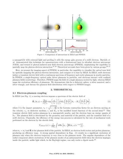
Figure 1. Comparison of interactions in EELS and PINEM.<br />
a nanoparticle with external light and probing it with the energy gain process of a swift electron. Barwick et.<br />
al. demonstrated this technique for nanostructures with a femtosecond laser in ultrafast electron microscopy<br />
(UEM), and termed it photon-induced near field electron microscopy (PINEM), emphasizing the capability to<br />
spatially map the photon-electron interaction. 27, 28 Theoretical accounts have been given by various groups. 29–31<br />
Here, we present the imaging aspect of PINEM, in particular, the capability to visualize the optical near field<br />
by spatially mapping the photon-electron interaction, and compare it to that by EELS. In EELS, swift electrons<br />
induce a transient electric field with a continuous spectrum of frequency and excite plasmons in nearby particles.<br />
In PINEM, a single-frequency optical pulse drives plasmons in particles, and electrons interact with confined<br />
plasmon fields (scattering). Therefore, PINEM maps the field of a single plasmon excited by light, whereas EELS<br />
maps the excitation efficiency of plasmons. We demonstrate this for a dielectric sphere, a silver nanorod, and a<br />
silver triangle, and discuss the plasmon field distribution with respect to PINEM images.<br />
2.1 <strong>Electron</strong>-plasmon coupling<br />
2. THEORETICAL<br />
In EELS (see Fig. 1), a moving electron imposes a spectrum of the electric field of<br />
Ẽ e (r, ω) = 2eω [<br />
ɛveγ 2 exp i ω ] [ i<br />
z<br />
ɛ v e<br />
γ ɛ<br />
K 0<br />
( ω<br />
v e<br />
) (<br />
b<br />
ω<br />
ˆv e − K 1<br />
γ ɛ v e<br />
)<br />
b<br />
ˆb<br />
γ ɛ<br />
]<br />
, (1)<br />
√<br />
where b is the impact parameter, γ ɛ = 1 − ɛ v2 e<br />
c<br />
is the Lorentz contraction factor for an electron moving at<br />
2<br />
the velocity, v e , in dielectric medium, ɛ, and K n is the modified bessel function of the second kind. 22 This<br />
transient electric field excites plasmons in a nanoparticle nearby, and the electron loses an energy quanta of<br />
¯hω. The plasmon field is determined by the geometry and material of the particle, and the transient field of a<br />
swift electron. Classically, the efficiency of the energy loss process is calculated by the rate of mechanical work<br />
performed on the electron by the electric field,<br />
Γ EELS (ω) =<br />
e<br />
π¯hω<br />
∫<br />
[<br />
dtRe v e ·<br />
{Ẽ (re , ω) e −iωt}] , (2)<br />
where r e = v e t and Ẽ is the plasmon field of the particle. In EELS, an electron both excites and probes plasmons,<br />
producing an efficiency map. A strong spatial dependence in Eqn. (1) results in a significant excitation of<br />
plasmon only when the electron trajectory is very close to the plasmon mode. The angular dependence of the<br />
radial component allows excitations of the plasmon modes of an antisymmetric field when the electron impinges<br />
inside the particle, unlike light which, in the Rayleigh regime, can only excite a dipole mode. 24<br />
Proc. of SPIE Vol. 8845 884506-2