

Application Note CoolMOS™ CP - Infineon
Application Note CoolMOS™ CP - Infineon
Application Note CoolMOS™ CP - Infineon

Create successful ePaper yourself
Turn your PDF publications into a flip-book with our unique Google optimized e-Paper software.
CoolMOS TM <strong>CP</strong><br />
- How to make most beneficial use of the latest<br />
generation of super junction technology devices<br />
This turn-off behavior is shown in the simulation<br />
results of Figure 10, displaying the gate input<br />
waveform, drain to source voltage, and drain<br />
current. In this mode, the gate drive retains<br />
complete control over the dv/dt of the MOSFET,<br />
and is directly sizable by adjusting the size of<br />
the gate input resistor. However, as gate charge<br />
becomes lower in MOSFETs, and output<br />
capacitance non-linearity increases, using small<br />
values of gate drive resistance eventually shifts<br />
the switch-off behavior into a different mode.<br />
Discharging 24<br />
the<br />
input capacitance Cgs + Cgd<br />
Gate voltage [V], Drain current [A]<br />
20<br />
16<br />
12<br />
8<br />
4<br />
Charging Cds<br />
Falling ID<br />
Vgs C3 [V]<br />
Ids C3 [A]<br />
Vds C3 [V]<br />
Discharging Cgs + Cgd<br />
500<br />
400<br />
300<br />
200<br />
100<br />
Charging Cgd<br />
0<br />
0<br />
0 20 40 60 80 100 120<br />
Time [ns]<br />
Drain voltage [V]<br />
3.2 Quasi-ZVS Switching<br />
Figure 10 Turn-off simulation of CoolMOS TM .<br />
Under conditions in which the gate drive turn-off is very fast, in<br />
combination with a relatively high Coss (as can exist in<br />
superjunction MOSFETs when the drain to source voltage is below<br />
50V), the switching behavior will be dominated by somewhat<br />
different mechanisms, and the drain switching voltage will not be<br />
controlled by the gate drive current, but by Coss and load current.<br />
The behavior can still be roughly described by three main states<br />
Figure 11 but externally measured gate drive or drain current can be<br />
misleading in identifying these states. The t1 state is governed<br />
similarly as for the gate controlled dv/dt mode; the difference arises<br />
in the t2 region, where the gate discharging current is at such a high<br />
level such that the load current cannot begin to charge a voltage<br />
across COSS, and the channel current is turned off before the drain<br />
to source voltage rises. This is approximately described by:<br />
⎛<br />
t2 = R G<br />
⋅C iss<br />
⋅ln V Plat<br />
− V G−Off<br />
⎞<br />
⎜<br />
⎝ V th<br />
− V<br />
⎟<br />
Figure 11 Quasi-ZVS Coss<br />
G−Off ⎠<br />
(5)<br />
controlled turn-off.<br />
This mode does result in very low turn-off losses, but it has some characteristics to consider that can become an<br />
issue in some applications, especially PFC converters with wide range of input current, and brief but high<br />
overloads.<br />
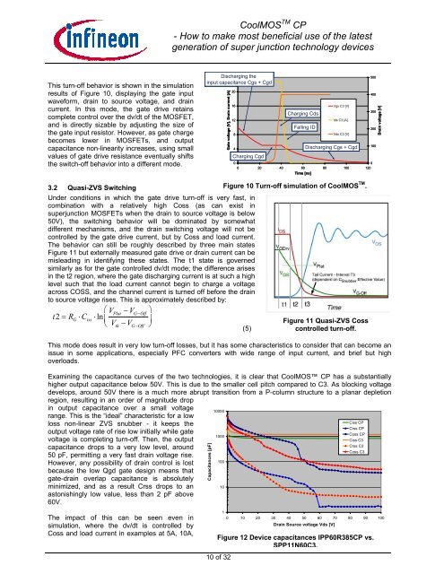
Examining the capacitance curves of the two technologies, it is clear that CoolMOS <strong>CP</strong> has a substantially<br />
higher output capacitance below 50V. This is due to the smaller cell pitch compared to C3. As blocking voltage<br />
develops, around 50V there is a much more abrupt transition from a P-column structure to a planar depletion<br />
region, resulting in an order of magnitude drop<br />
in output capacitance over a small voltage<br />
10000<br />
range. This is the “ideal” characteristic for a low<br />
Ciss <strong>CP</strong><br />
loss non-linear ZVS snubber - it keeps the<br />
Crss <strong>CP</strong><br />
output voltage rate of rise low initially while gate<br />
Coss <strong>CP</strong><br />
1000<br />
voltage is completing turn-off. Then, the output<br />
Ciss C3<br />
Crss C3<br />
capacitance drops to a very low level, around<br />
Coss C3<br />
50 pF, permitting a very fast drain voltage rise.<br />
100<br />
However, any possibility of drain control is lost<br />
because the low Qgd gate design means that<br />
gate-drain overlap capacitance is absolutely<br />
minimized, and as a result Crss drops to an<br />
10<br />
astonishingly low value, less than 2 pF above<br />
60V.<br />
Capacitances [pF]<br />
The impact of this can be seen even in<br />
simulation, where the dv/dt is controlled by<br />
Coss and load current in examples at 5A, 10A,<br />
10 of 32<br />
1<br />
0 10 20 30 40 50 60 70 80 90 100<br />
Drain Source voltage Vds [V]<br />
Figure 12 Device capacitances IPP60R385<strong>CP</strong> vs.<br />
SPP11N60C3.


