

Application Note CoolMOS™ CP - Infineon
Application Note CoolMOS™ CP - Infineon
Application Note CoolMOS™ CP - Infineon

You also want an ePaper? Increase the reach of your titles
YUMPU automatically turns print PDFs into web optimized ePapers that Google loves.
CoolMOS TM <strong>CP</strong><br />
- How to make most beneficial use of the latest<br />
generation of super junction technology devices<br />
1.1 The Superjunction principle<br />
CoolMOS TM is a revolutionary technology for<br />
high voltage power MOSFETs and designed<br />
according to the superjunction (SJ) principle<br />
[1], which in turn is based on the RESURF [2]<br />
ideas being successfully used for decades in<br />
lateral power MOSFETs. Conventional power<br />
MOSFETs suffer from the limitation of the socalled<br />
silicon limit [3], which means that<br />
doubling the voltage blocking capability<br />
typically leads to an increase in the on-state<br />
resistance by a factor of five. The silicon limit<br />
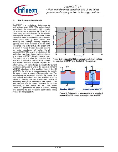
is shown in Figure 2 where the area specific<br />
on state resistance of state-of-the-art<br />
standard MOSFETs as well are indicated. SJ<br />
technology may lower the on-state resistance<br />
of a power MOSFET virtually towards zero.<br />
The basic idea is to allow the current to flow<br />
from top to bottom of the MOSFET in very<br />
high doped vertically arranged regions. In<br />
other words, a lot more charge is available for current<br />
conduction compared to what is the case in a standard<br />
MOSFET structure. In the blocking state of the SJ<br />
MOSFET, the charge is counterbalanced by exactly<br />
the same amount of charge of the opposite type. The<br />
two charges are separated locally in the device by a<br />
very refined technology, and the resulting structure<br />
shows a laterally stacked fine-pitched pattern of<br />
alternating arranged p- and n-areas, see Figure 1. The<br />
finer the pitch can be made, the lower the on-state<br />
resistance of the device will be. With every<br />
CoolMOS TM generation the pitch is reduced, moving<br />
ever closer to the zero resistance point without losing<br />
voltage blocking capability.<br />
RDSon*A [Ohm*mm 2 ]<br />
12<br />
10<br />
8<br />
6<br />
4<br />
2<br />
State-of-the-art<br />
standard MOSFETs<br />
CoolMOS TM <strong>CP</strong><br />
Si Limit<br />
CoolMOS TM C3<br />
0<br />
400 500 600 700 800 900<br />
Breakdown Voltage [V]<br />
Figure 2 Area-specific RDSon versus breakdown voltage<br />
for standard MOSFET and CoolMOS TM technology.<br />
S<br />
G<br />
D<br />
Standard MOSFET<br />
S<br />
n<br />
p +<br />
p -<br />
p<br />
n + sub<br />
G<br />
-<br />
-<br />
-<br />
n epi<br />
D<br />
- -<br />
-<br />
Superjunction MOSFET<br />
Figure 1 Schematic cross-section of a standard<br />
power MOSFET versus a superjunction MOSFET<br />
4 of 32


