

Application Note CoolMOS™ CP - Infineon
Application Note CoolMOS™ CP - Infineon
Application Note CoolMOS™ CP - Infineon

You also want an ePaper? Increase the reach of your titles
YUMPU automatically turns print PDFs into web optimized ePapers that Google loves.
CoolMOS TM <strong>CP</strong><br />
- How to make most beneficial use of the latest<br />
generation of super junction technology devices<br />
2 Technology Comparison of CoolMOS TM <strong>CP</strong> to C3<br />
CoolMOS <strong>CP</strong> is the next step towards THE IDEAL HIGH VOLTAGE SWITCH with key features:<br />
Further reduced conduction and switching losses<br />
Lowest on-state-resistance per package @600V blocking capability<br />
Ultra-low gate charge and Lowest figure-of-merit R DSon x Q g<br />
… which gives the application benefits:<br />
Extremely reduced heat generation<br />
Reduced system size and weight<br />
Very low gate drive power facilitating the use of low cost ICs and gate drivers<br />
Reduced overall system cost<br />
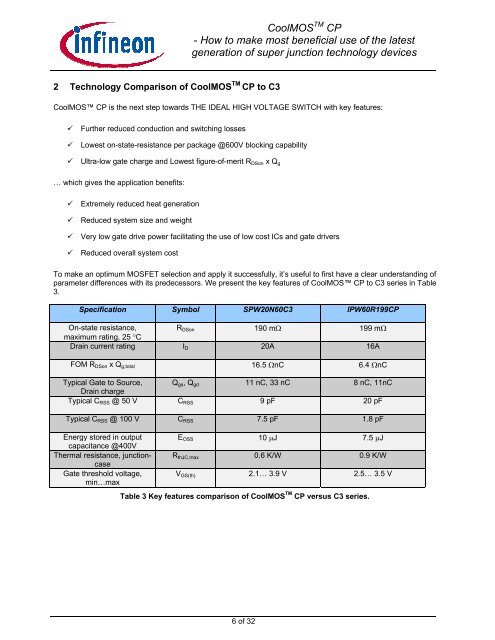
To make an optimum MOSFET selection and apply it successfully, it’s useful to first have a clear understanding of<br />
parameter differences with its predecessors. We present the key features of CoolMOS <strong>CP</strong> to C3 series in Table<br />
3.<br />
Specification Symbol SPW20N60C3 IPW60R199<strong>CP</strong><br />
On-state resistance,<br />
R DSon 190 mΩ 199 mΩ<br />
maximum rating, 25 °C<br />
Drain current rating I D 20A 16A<br />
FOM R DSon x Q g,total 16.5 ΩnC 6.4 ΩnC<br />
Typical Gate to Source, Q gs , Q gd 11 nC, 33 nC 8 nC, 11nC<br />
Drain charge<br />
Typical C RSS @ 50 V C RSS 9 pF 20 pF<br />
Typical C RSS @ 100 V C RSS 7.5 pF 1.8 pF<br />
Energy stored in output<br />
capacitance @400V<br />
Thermal resistance, junctioncase<br />
Gate threshold voltage,<br />
min…max<br />
E OSS 10 µJ 7.5 µJ<br />
R thJC,max 0.6 K/W 0.9 K/W<br />
V GS(th) 2.1… 3.9 V 2.5… 3.5 V<br />
Table 3 Key features comparison of CoolMOS TM <strong>CP</strong> versus C3 series.<br />
6 of 32


