

Application Note CoolMOS™ CP - Infineon
Application Note CoolMOS™ CP - Infineon
Application Note CoolMOS™ CP - Infineon

Create successful ePaper yourself
Turn your PDF publications into a flip-book with our unique Google optimized e-Paper software.
CoolMOS TM <strong>CP</strong><br />
- How to make most beneficial use of the latest<br />
generation of super junction technology devices<br />
4200<br />
180<br />
di/dt, turn off [A/µs]<br />
3500<br />
2800<br />
2100<br />
1400<br />
C3 at Rg=3.6 Ohm<br />
<strong>CP</strong> at Rg=6.8 Ohm<br />
<strong>CP</strong> at Rg=68 Ohm<br />
No gate control, excessive di/dt<br />
transition region<br />
dv/dt, turn off [V/ns]<br />
150<br />
120<br />
90<br />
60<br />
C3 at Rg=3.6 Ohm<br />
<strong>CP</strong> at Rg=6.8 Ohm<br />
<strong>CP</strong> at Rg=68 Ohm<br />
dv/dt limited by Coss<br />
transition region<br />
700<br />
Full control by Rg,<br />
no current dependency on di/dt<br />
0<br />
0 5 10 15 20 25<br />
Load current [A]<br />
30<br />
dv/dt controlled by Rg<br />
0<br />
0 5 10 15 20 25<br />
Load current [A]<br />
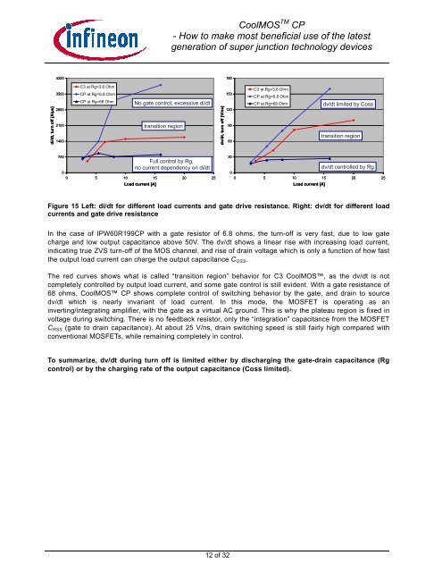
Figure 15 Left: di/dt for different load currents and gate drive resistance. Right: dv/dt for different load<br />
currents and gate drive resistance<br />
In the case of IPW60R199<strong>CP</strong> with a gate resistor of 6.8 ohms, the turn-off is very fast, due to low gate<br />
charge and low output capacitance above 50V. The dv/dt shows a linear rise with increasing load current,<br />
indicating true ZVS turn-off of the MOS channel, and rise of drain voltage which is only a function of how fast<br />
the output load current can charge the output capacitance C OSS .<br />
The red curves shows what is called “transition region” behavior for C3 CoolMOS, as the dv/dt is not<br />
completely controlled by output load current, and some gate control is still evident. With a gate resistance of<br />
68 ohms, CoolMOS <strong>CP</strong> shows complete control of switching behavior by the gate, and drain to source<br />
dv/dt which is nearly invariant of load current. In this mode, the MOSFET is operating as an<br />
inverting/integrating amplifier, with the gate as a virtual AC ground. This is why the plateau region is fixed in<br />
voltage during switching. There is no feedback resistor, only the “integration” capacitance from the MOSFET<br />
C RSS (gate to drain capacitance). At about 25 V/ns, drain switching speed is still fairly high compared with<br />
conventional MOSFETs, while remaining completely in control.<br />
To summarize, dv/dt during turn off is limited either by discharging the gate-drain capacitance (Rg<br />
control) or by the charging rate of the output capacitance (Coss limited).<br />
12 of 32


