

Darlington Transistor NPN - ON Semiconductor
Darlington Transistor NPN - ON Semiconductor
Darlington Transistor NPN - ON Semiconductor

You also want an ePaper? Increase the reach of your titles
YUMPU automatically turns print PDFs into web optimized ePapers that Google loves.
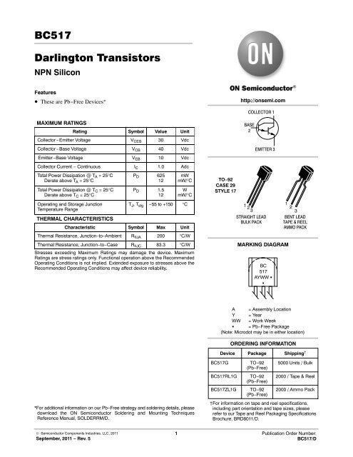
BC517<br />
<strong>Darlington</strong> <strong>Transistor</strong>s<br />
<strong>NPN</strong> Silicon<br />
Features<br />
• These are Pb−Free Devices*<br />
http://onsemi.com<br />
MAXIMUM RATINGS<br />
Rating Symbol Value Unit<br />
Collector−Emitter Voltage V CES 30 Vdc<br />
Collector−Base Voltage V CB 40 Vdc<br />
Emitter−Base Voltage V EB 10 Vdc<br />
Collector Current − Continuous I C 1.0 Adc<br />
Total Power Dissipation @ T A = 25°C<br />
Derate above T A = 25°C<br />
Total Power Dissipation @ T C = 25°C<br />
Derate above T C = 25°C<br />
P D 625<br />
12<br />
P D 1.5<br />
12<br />
mW<br />
mW/°C<br />
W<br />
mW/°C<br />
TO−92<br />
CASE 29<br />
STYLE 17<br />
COLLECTOR 1<br />
BASE<br />
2<br />
EMITTER 3<br />
Operating and Storage Junction<br />
Temperature Range<br />
THERMAL CHARACTERISTICS<br />
T J , T stg −55 to +150 °C<br />
Characteristic Symbol Max Unit<br />
Thermal Resistance, Junction−to−Ambient R JA 200 °C/W<br />
Thermal Resistance, Junction−to−Case R JC 83.3 °C/W<br />
Stresses exceeding Maximum Ratings may damage the device. Maximum<br />
Ratings are stress ratings only. Functional operation above the Recommended<br />
Operating Conditions is not implied. Extended exposure to stresses above the<br />
Recommended Operating Conditions may affect device reliability.<br />
1 1<br />
2 2<br />
3 3<br />
STRAIGHT LEAD BENT LEAD<br />
BULK PACK<br />
TAPE & REEL<br />
AMMO PACK<br />
MARKING DIAGRAM<br />
BC<br />
517<br />
AYWW <br />
<br />
A = Assembly Location<br />
Y = Year<br />
WW = Work Week<br />
= Pb−Free Package<br />
(Note: Microdot may be in either location)<br />
ORDERING INFORMATI<strong>ON</strong><br />
Device Package Shipping †<br />
*For additional information on our Pb−Free strategy and soldering details, please<br />
download the <strong>ON</strong> <strong>Semiconductor</strong> Soldering and Mounting Techniques<br />
Reference Manual, SOLDERRM/D.<br />
BC517G<br />
BC517RL1G<br />
BC517ZL1G<br />
TO−92<br />
(Pb−Free)<br />
TO−92<br />
(Pb−Free)<br />
TO−92<br />
(Pb−Free)<br />
5000 Units / Bulk<br />
2000 / Tape & Reel<br />
2000 / Ammo Pack<br />
†For information on tape and reel specifications,<br />
including part orientation and tape sizes, please<br />
refer to our Tape and Reel Packaging Specifications<br />
Brochure, BRD8011/D.<br />
© <strong>Semiconductor</strong> Components Industries, LLC, 2011<br />
September, 2011 − Rev. 5<br />
1 Publication Order Number:<br />
BC517/D
BC517<br />
ELECTRICAL CHARACTERISTICS (T A = 25°C unless otherwise noted)<br />
Characteristic Symbol Min Typ Max Unit<br />
OFF CHARACTERISTICS<br />
Collector−Emitter Breakdown Voltage<br />
(I C = 2.0 mAdc, I BE = 0)<br />
V (BR)CES<br />
30 − −<br />
Vdc<br />
Collector−Base Breakdown Voltage<br />
(I C = 10 Adc, I E = 0)<br />
Emitter−Base Breakdown Voltage<br />
(I E = 100 Adc, I C = 0)<br />
Collector Cutoff Current<br />
(V CE = 30 Vdc)<br />
Collector Cutoff Current<br />
(V CB = 30 Vdc, I E = 0)<br />
Emitter Cutoff Current<br />
(V CB = 10 Vdc, I C = 0)<br />
<strong>ON</strong> CHARACTERISTICS (Note 1)<br />
DC Current Gain<br />
(I C = 20 mAdc, V CE = 2.0 Vdc)<br />
Collector−Emitter Saturation Voltage<br />
(I C = 100 mAdc, I B = 0.1 mAdc)<br />
Collector−Emitter Saturation Voltage<br />
(I C = 10 mAdc, V CE = 5.0 Vdc)<br />
SMALL−SIGNAL CHARACTERISTICS<br />
Current−Gain − Bandwidth Product (Note 2)<br />
(I C = 10 mAdc, V CE = 5.0 Vdc, f = 100 MHz)<br />
1. Pulse Test: Pulse Width = 300 s, Duty Cycle 2.0%.<br />
2. f T = |h fe | • f test<br />
R S<br />
i n<br />
(BR)CBO<br />
40 − −<br />
V (BR)EBO<br />
10 − −<br />
I CES<br />
− − 500<br />
I CBO<br />
− − 100<br />
I EBO<br />
− − 100<br />
h FE<br />
30,000 − −<br />
V CE(sat)<br />
− − 1.0<br />
V BE(on)<br />
− − 1.4<br />
f T<br />
− 200 −<br />
Vdc<br />
Vdc<br />
nAdc<br />
nAdc<br />
nAdc<br />
−<br />
Vdc<br />
Vdc<br />
MHz<br />
e n<br />
IDEAL<br />
TRANSISTOR<br />
Figure 1. <strong>Transistor</strong> Noise Model<br />
http://onsemi.com<br />
2
BC517<br />
NOISE CHARACTERISTICS<br />
(V CE = 5.0 Vdc, T A = 25°C)<br />
en, NOISE VOLTAGE (nV)<br />
500<br />
200<br />
100<br />
50<br />
20<br />
10<br />
5.0<br />
10<br />
BANDWIDTH = 1.0 Hz<br />
R S ≈ 0<br />
20 50 100 200 500 1k 2k 5k 10k 20k 50k 100k<br />
f, FREQUENCY (Hz)<br />
100 A<br />
I C = 1.0 mA<br />
10 A<br />
in, NOISE CURRENT (pA)<br />
2.0<br />
1.0<br />
0.7<br />
0.5<br />
0.3<br />
0.2<br />
BANDWIDTH = 1.0 Hz<br />
I C = 1.0 mA<br />
0.1<br />
0.07<br />
0.05<br />
100 A<br />
10 A<br />
0.03<br />
0.02<br />
10 20 50 100 200 500 1k 2k 5k 10k 20k 50k 100k<br />
f, FREQUENCY (Hz)<br />
Figure 2. Noise Voltage<br />
Figure 3. Noise Current<br />
VT, TOTAL WIDEBAND NOISE VOLTAGE (nV)<br />
200<br />
100<br />
70<br />
50<br />
30<br />
20<br />
10<br />
1.0<br />
BANDWIDTH = 10 Hz TO 15.7 kHz<br />
I C = 10 A<br />
100 A<br />
1.0 mA<br />
2.0 5.0 10 20 50 100 200 500 1000<br />
R S , SOURCE RESISTANCE (k)<br />
Figure 4. Total Wideband Noise Voltage<br />
NF, NOISE FIGURE (dB)<br />
14<br />
BANDWIDTH = 10 Hz TO 15.7 kHz<br />
12<br />
10<br />
10 A<br />
8.0<br />
100 A<br />
6.0<br />
4.0 I C = 1.0 mA<br />
2.0<br />
0<br />
1.0 2.0 5.0 10 20 50 100 200 500 1000<br />
R S , SOURCE RESISTANCE (k)<br />
Figure 5. Wideband Noise Figure<br />
http://onsemi.com<br />
3
BC517<br />
SMALL−SIGNAL CHARACTERISTICS<br />
C, CAPACITANCE (pF)<br />
20<br />
10<br />
7.0<br />
5.0<br />
3.0<br />
T J = 25°C<br />
|hfe|, SMALL-SIGNAL CURRENT GAIN<br />
4.0<br />
2.0<br />
1.0<br />
0.8<br />
0.6<br />
0.4<br />
V CE = 5.0 V<br />
f = 100 MHz<br />
T J = 25°C<br />
2.0<br />
0.04<br />
0.1 0.2 0.4 1.0 2.0 4.0 10 20 40<br />
V R , REVERSE VOLTAGE (VOLTS)<br />
0.2<br />
C ibo<br />
C obo<br />
0.5 1.0 2.0 0.5 10 20 50 100 200 500<br />
I C , COLLECTOR CURRENT (mA)<br />
Figure 6. Capacitance<br />
Figure 7. High Frequency Current Gain<br />
hFE, DC CURRENT GAIN<br />
200k<br />
100k<br />
70k<br />
50k<br />
30k<br />
20k<br />
10k<br />
7.0k<br />
5.0k<br />
3.0k<br />
T J = 125°C<br />
25°C<br />
-55°C<br />
2.0k<br />
5.0 7.0 10 20 30 50 70 100 200 300 500<br />
I C , COLLECTOR CURRENT (mA)<br />
Figure 8. DC Current Gain<br />
V CE = 5.0 V<br />
VCE, COLLECTOR-EMITTER VOLTAGE (VOLTS)<br />
3.0<br />
T J = 25°C<br />
2.5<br />
I C = 10 mA 50 mA 250 mA 500 mA<br />
2.0<br />
1.5<br />
1.0<br />
0.5<br />
0.1 0.2 0.5 1.0 2.0 5.0 10 20 50 100 200 500 1000<br />
I B , BASE CURRENT (A)<br />
Figure 9. Collector Saturation Region<br />
V, VOLTAGE (VOLTS)<br />
1.6<br />
1.4<br />
1.2<br />
1.0<br />
0.8<br />
0.6<br />
5.0<br />
T J = 25°C<br />
V BE(sat) @ I C /I B = 1000<br />
V BE(on) @ V CE = 5.0 V<br />
V CE(sat) @ I C /I B = 1000<br />
7.0 10 20 30 50 70 100 200 300 500<br />
I C , COLLECTOR CURRENT (mA)<br />
R θ V, TEMPERATURE COEFFICIENTS (mV/ ° C)<br />
-1.0<br />
-2.0<br />
-3.0<br />
-4.0<br />
-5.0<br />
*APPLIES FOR I C /I B ≤ h FE /3.0<br />
*R VC FOR V CE(sat)<br />
25°C TO 125°C<br />
-55°C TO 25°C<br />
VB FOR V BE<br />
25°C TO 125°C<br />
-55°C TO 25°C<br />
-6.0<br />
5.0 7.0 10 20 30 50 70 100 200 300 500<br />
I C , COLLECTOR CURRENT (mA)<br />
Figure 10. “On” Voltages<br />
Figure 11. Temperature Coefficients<br />
http://onsemi.com<br />
4
BC517<br />
()<br />
RESISTANCE (NORMALIZED)<br />
1.0<br />
0.7<br />
0.5<br />
0.3<br />
0.2<br />
0.1<br />
0.07<br />
0.05<br />
0.03<br />
0.02<br />
D = 0.5<br />
0.2<br />
0.1<br />
0.05 SINGLE PULSE<br />
SINGLE PULSE<br />
Z JC(t) = r(t) • R JC T J(pk) - T C = P (pk) Z JC(t)<br />
Z JA(t) = r(t) • R JA T J(pk) - T A = P (pk) Z JA(t)<br />
0.01<br />
0.1<br />
0.2<br />
0.5<br />
1.0<br />
2.0 5.0<br />
10 20 50 100 200 500 1.0k 2.0k 5.0k 10k<br />
t, TIME (ms)<br />
Figure 12. Thermal Response<br />
IC, COLLECTOR CURRENT (mA)<br />
1.0k<br />
700<br />
500<br />
300<br />
200<br />
100<br />
70<br />
50<br />
30<br />
20<br />
10<br />
0.4<br />
T A = 25°C<br />
T C = 25°C<br />
CURRENT LIMIT<br />
THERMAL LIMIT<br />
SEC<strong>ON</strong>D BREAKDOWN LIMIT<br />
1.0 ms<br />
1.0 s<br />
100 s<br />
0.6 1.0 2.0 4.0 6.0 10 20 40<br />
V CE , COLLECTOR-EMITTER VOLTAGE (VOLTS)<br />
FIGURE A<br />
P P<br />
t P<br />
t 1<br />
1/f<br />
DUTYCYCLE t1f t 1<br />
tP<br />
PEAK PULSE POWER = P P<br />
P P<br />
Figure 13. Active Region Safe Operating Area<br />
Design Note: Use of Transient Thermal Resistance Data<br />
http://onsemi.com<br />
5
BC517<br />
PACKAGE DIMENSI<strong>ON</strong>S<br />
TO−92 (TO−226)<br />
CASE 29−11<br />
ISSUE AM<br />
R<br />
A<br />
N<br />
B<br />
STRAIGHT LEAD<br />
BULK PACK<br />
NOTES:<br />
1. DIMENSI<strong>ON</strong>ING AND TOLERANCING PER ANSI<br />
Y14.5M, 1982.<br />
2. C<strong>ON</strong>TROLLING DIMENSI<strong>ON</strong>: INCH.<br />
3. C<strong>ON</strong>TOUR OF PACKAGE BEY<strong>ON</strong>D DIMENSI<strong>ON</strong> R<br />
IS UNC<strong>ON</strong>TROLLED.<br />
4. LEAD DIMENSI<strong>ON</strong> IS UNC<strong>ON</strong>TROLLED IN P AND<br />
BEY<strong>ON</strong>D DIMENSI<strong>ON</strong> K MINIMUM.<br />
P<br />
L<br />
SEATING<br />
INCHES MILLIMETERS<br />
PLANE K<br />
DIM MIN MAX MIN MAX<br />
A 0.175 0.205 4.45 5.20<br />
B 0.170 0.210 4.32 5.33<br />
C 0.125 0.165 3.18 4.19<br />
D 0.016 0.021 0.407 0.533<br />
X X<br />
D<br />
G 0.045 0.055 1.15 1.39<br />
H 0.095 0.105 2.42 2.66<br />
G<br />
J 0.015 0.020 0.39 0.50<br />
H<br />
J<br />
K 0.500 --- 12.70 ---<br />
V<br />
C<br />
L 0.250 --- 6.35 ---<br />
N 0.080 0.105 2.04 2.66<br />
P --- 0.100 --- 2.54<br />
SECTI<strong>ON</strong> X−X<br />
R 0.115 --- 2.93 ---<br />
1 N<br />
V 0.135 --- 3.43 ---<br />
R<br />
T<br />
SEATING<br />
PLANE<br />
P<br />
G<br />
A<br />
X X<br />
V<br />
1<br />
B<br />
K<br />
C<br />
N<br />
BENT LEAD<br />
TAPE & REEL<br />
AMMO PACK<br />
D<br />
J<br />
SECTI<strong>ON</strong> X−X<br />
NOTES:<br />
1. DIMENSI<strong>ON</strong>ING AND TOLERANCING PER<br />
ASME Y14.5M, 1994.<br />
2. C<strong>ON</strong>TROLLING DIMENSI<strong>ON</strong>: MILLIMETERS.<br />
3. C<strong>ON</strong>TOUR OF PACKAGE BEY<strong>ON</strong>D<br />
DIMENSI<strong>ON</strong> R IS UNC<strong>ON</strong>TROLLED.<br />
4. LEAD DIMENSI<strong>ON</strong> IS UNC<strong>ON</strong>TROLLED IN P<br />
AND BEY<strong>ON</strong>D DIMENSI<strong>ON</strong> K MINIMUM.<br />
MILLIMETERS<br />
DIM MIN MAX<br />
A 4.45 5.20<br />
B 4.32 5.33<br />
C 3.18 4.19<br />
D 0.40 0.54<br />
G 2.40 2.80<br />
J 0.39 0.50<br />
K 12.70 ---<br />
N 2.04 2.66<br />
P 1.50 4.00<br />
R 2.93 ---<br />
V 3.43 ---<br />
STYLE 17:<br />
PIN 1. COLLECTOR<br />
2. BASE<br />
3. EMITTER<br />
<strong>ON</strong> <strong>Semiconductor</strong> and are registered trademarks of <strong>Semiconductor</strong> Components Industries, LLC (SCILLC). SCILLC reserves the right to make changes without further notice<br />
to any products herein. SCILLC makes no warranty, representation or guarantee regarding the suitability of its products for any particular purpose, nor does SCILLC assume any liability<br />
arising out of the application or use of any product or circuit, and specifically disclaims any and all liability, including without limitation special, consequential or incidental damages.<br />
“Typical” parameters which may be provided in SCILLC data sheets and/or specifications can and do vary in different applications and actual performance may vary over time. All<br />
operating parameters, including “Typicals” must be validated for each customer application by customer’s technical experts. SCILLC does not convey any license under its patent rights<br />
nor the rights of others. SCILLC products are not designed, intended, or authorized for use as components in systems intended for surgical implant into the body, or other applications<br />
intended to support or sustain life, or for any other application in which the failure of the SCILLC product could create a situation where personal injury or death may occur. Should<br />
Buyer purchase or use SCILLC products for any such unintended or unauthorized application, Buyer shall indemnify and hold SCILLC and its officers, employees, subsidiaries, affiliates,<br />
and distributors harmless against all claims, costs, damages, and expenses, and reasonable attorney fees arising out of, directly or indirectly, any claim of personal injury or death<br />
associated with such unintended or unauthorized use, even if such claim alleges that SCILLC was negligent regarding the design or manufacture of the part. SCILLC is an Equal<br />
Opportunity/Affirmative Action Employer. This literature is subject to all applicable copyright laws and is not for resale in any manner.<br />
PUBLICATI<strong>ON</strong> ORDERING INFORMATI<strong>ON</strong><br />
LITERATURE FULFILLMENT:<br />
Literature Distribution Center for <strong>ON</strong> <strong>Semiconductor</strong><br />
P.O. Box 5163, Denver, Colorado 80217 USA<br />
Phone: 303−675−2175 or 800−344−3860 Toll Free USA/Canada<br />
Fax: 303−675−2176 or 800−344−3867 Toll Free USA/Canada<br />
Email: orderlit@onsemi.com<br />
N. American Technical Support: 800−282−9855 Toll Free<br />
USA/Canada<br />
Europe, Middle East and Africa Technical Support:<br />
Phone: 421 33 790 2910<br />
Japan Customer Focus Center<br />
Phone: 81−3−5773−3850<br />
http://onsemi.com<br />
6<br />
<strong>ON</strong> <strong>Semiconductor</strong> Website: www.onsemi.com<br />
Order Literature: http://www.onsemi.com/orderlit<br />
For additional information, please contact your local<br />
Sales Representative<br />
BC517/D


