

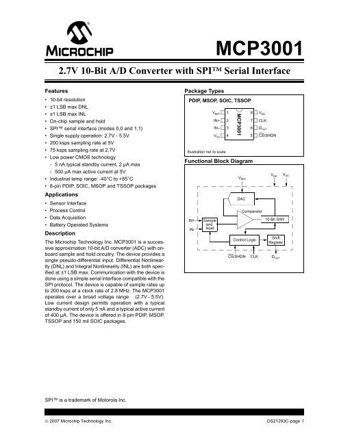
MCP3001 2.7V 10-Bit A/D Converter with SPI Serial ... - Microchip
MCP3001 2.7V 10-Bit A/D Converter with SPI Serial ... - Microchip
MCP3001 2.7V 10-Bit A/D Converter with SPI Serial ... - Microchip

Create successful ePaper yourself
Turn your PDF publications into a flip-book with our unique Google optimized e-Paper software.
<strong>MCP3001</strong>Load circuit for t R , t F , t DO1.4V3kΩ Test PointD OUTC L = 30 pFD OUTLoad circuit for t DIS and t ENTest Pointt DIS Waveform 23kΩ30 pFV DDV DD/2t EN Waveformt DIS Waveform 1CSCLKV SS3 4Voltage Waveforms for t R , t FVoltage Waveforms for t END OUTt RV OHV OLt F1 2D OUTB9t ENVoltage Waveforms for t DOVoltage Waveforms for t DISCLKt DOCSD OUTWaveform 1*V IH90%t DISD OUTD OUTWaveform 2†<strong>10</strong>%* Waveform 1 is for an output <strong>with</strong> internal conditionssuch that the output is high, unless disabledby the output control.† Waveform 2 is for an output <strong>with</strong> internal conditionssuch that the output is low, unless disabledby the output control.FIGURE 1-2:Test Circuits.© 2007 <strong>Microchip</strong> Technology Inc. DS21293C-page 5
<strong>MCP3001</strong>Note: Unless otherwise indicated, V DD = V REF = 5V, f SAMPLE = 200 ksps, f CLK = 14*Sample Rate,T A = 25°CIDD (µA)500450400350300250200150V REF = V DD<strong>10</strong>0All points at f CLK = 2.8 MHz except50 at V REF = V DD = 2.5V, f CLK =1.05 MHz02.0 2.5 3.0 3.5 4.0 4.5 5.0 5.5 6.0V DD (V)IREF (µA)1201<strong>10</strong><strong>10</strong>090807060504030 V REF = V DD20 All points at f CLK = 2.8 MHz except<strong>10</strong> at V REF = V DD = 2.5V, f CLK = 1.05 MHz02.0 2.5 3.0 3.5 4.0 4.5 5.0 5.5 6.0V DD (V)FIGURE 2-31: I DD vs. V DD .FIGURE 2-34: I REF vs. V DD .IDD (µA)500450400350300 VDD = VREF = 5V250200150VDD = VREF = <strong>2.7V</strong><strong>10</strong>0500<strong>10</strong> <strong>10</strong>0 <strong>10</strong>00 <strong>10</strong>000IREF (µA)1201<strong>10</strong><strong>10</strong>090V DD = V REF = 5V8070605040V DD = V REF = <strong>2.7V</strong>3020<strong>10</strong>0<strong>10</strong> <strong>10</strong>0 <strong>10</strong>00 <strong>10</strong>000Clock Frequency (kHz)Clock Frequency (kHz)FIGURE 2-32: I DD vs. Clock Frequency.FIGURE 2-35: I REF vs. Clock Frequency.IDD (µA)600550500450400350V DD = V REF = 5Vf CLK = 2.8 MHz300250200150V DD = V REF = <strong>2.7V</strong><strong>10</strong>050f CLK = 1.05 MHz0-50 -25 0 25 50 75 <strong>10</strong>0Temperature (°C)IREF (µA)1201<strong>10</strong><strong>10</strong>09080706050403020V DD = V REF = <strong>2.7V</strong>f CLK = 1.05 MHzV DD = V REF = 5Vf CLK = 2.8 MHz<strong>10</strong>0-50 -25 0 25 50 75 <strong>10</strong>0Temperature (°C)FIGURE 2-33: I DD vs. Temperature.FIGURE 2-36: I REF vs. Temperature.© 2007 <strong>Microchip</strong> Technology Inc. DS21293C-page 11
<strong>MCP3001</strong>Note: Unless otherwise indicated, V DD = V REF = 5V, f SAMPLE = 200 ksps, f CLK = 14*Sample Rate,T A = 25°CIDDS (pA)60VREF = CS = VDD50403020<strong>10</strong>02.0 2.5 3.0 3.5 4.0 4.5 5.0 5.5 6.0V DD (V)Analog Input Leakage (nA)2.01.8 V DD = V REF = 5V1.61.41.21.00.80.60.40.20.0-50 -25 0 25 50 75 <strong>10</strong>0Temperature (°C)FIGURE 2-37: I DDS vs. V DD .FIGURE 2-39: Analog Input Leakage Current vs.Temperature.<strong>10</strong>0.00V DD = V REF = CS = 5V<strong>10</strong>.00IDDS (nA)1.000.<strong>10</strong>0.01-50 -25 0 25 50 75 <strong>10</strong>0Temperature (°C)FIGURE 2-38: I DDS vs. Temperature.DS21293C-page 12© 2007 <strong>Microchip</strong> Technology Inc.
<strong>MCP3001</strong>3.0 PIN DESCRIPTIONS3.1 IN+Positive analog input. This input can vary from IN- toV REF + IN-.3.2 IN-Negative analog input. This input can vary ±<strong>10</strong>0 mVfrom V SS .3.3 CS/SHDN(Chip Select/Shutdown)The CS/SHDN pin is used to initiate communication<strong>with</strong> the device when pulled low and will end a conversionand put the device in low power standby whenpulled high. The CS/SHDN pin must be pulled highbetween conversions.3.4 CLK (<strong>Serial</strong> Clock)The <strong>SPI</strong> clock pin is used to initiate a conversion and toclock out each bit of the conversion as it takes place.See Section 6.2 for constraints on clock speed.3.5 DOUT (<strong>Serial</strong> Data output)The <strong>SPI</strong> serial data output pin is used to shift out theresults of the A/D conversion. Data will always changeon the falling edge of each clock as the conversiontakes place.4.0 DEVICE OPERATIONThe <strong>MCP3001</strong> A/D converter employs a conventionalSAR architecture. With this architecture, a sample isacquired on an internal sample/hold capacitor for1.5 clock cycles starting on the first rising edge of theserial clock after CS has been pulled low. Following thissample time, the input switch of the converter opensand the device uses the collected charge on the internalsample and hold capacitor to produce a serial <strong>10</strong>-bitdigital output code. Conversion rates of 200 ksps arepossible on the <strong>MCP3001</strong>. See Section 6.2 for informationon minimum clock rates. Communication <strong>with</strong> thedevice is done using a 3-wire <strong>SPI</strong>-compatible interface.In this diagram, it is shown that the source impedance(R S ) adds to the internal sampling switch, (R SS ) impedance,directly affecting the time that is required tocharge the capacitor, C SAMPLE . Consequently, a largersource impedance increases the offset, gain, and integrallinearity errors of the conversion.Ideally, the impedance of the signal source should benear zero. This is achievable <strong>with</strong> an operational amplifiersuch as the MCP601, which has a closed loop outputimpedance of tens of ohms. The adverse affects ofhigher source impedances are shown in Figure 4-2.If the voltage level of IN+ is equal to or less than IN-, theresultant code will be 000h. If the voltage at IN+ is equalto or greater than {[V REF + (IN-)] - 1 LSB}, then the outputcode will be 3FFh. If the voltage level at IN- is morethan 1 LSB below V SS , then the voltage level at the IN+input will have to go below V SS to see the 000h outputcode. Conversely, if IN- is more than 1 LSB above Vss,then the 3FFh code will not be seen unless the IN+input level goes above V REF level.4.2 Reference InputThe reference input (V REF ) determines the analog inputvoltage range and the LSB size, as shown below.LSB Size =V REF------------<strong>10</strong>24As the reference input is reduced, the LSB size isreduced accordingly. The theoretical digital output codeproduced by the A/D <strong>Converter</strong> is a function of the analoginput signal and the reference input as shownbelow.<strong>10</strong>24*V INDigital Output Code = -----------------------V REF4.1 Analog InputsThe <strong>MCP3001</strong> provides a single pseudo-differentialinput. The IN+ input can range from IN- to (V REF +IN-).The IN- input is limited to ±<strong>10</strong>0 mV from the V SS rail.The IN- input can be used to cancel small signal common-modenoise which is present on both the IN+ andIN- inputs.For the A/D <strong>Converter</strong> to meet specification, the chargeholding capacitor, C SAMPLE must be given enough timeto acquire a <strong>10</strong>-bit accurate voltage level during the1.5 clock cycle sampling period. The analog inputmodel is shown in Figure 4-1.where:V IN = analog input voltage = V(IN+) - V(IN-)V REF = reference voltageWhen using an external voltage reference device, thesystem designer should always refer to the manufacturer’srecommendations for circuit layout. Any instabilityin the operation of the reference device will have adirect effect on the operation of the ADC.© 2007 <strong>Microchip</strong> Technology Inc. DS21293C-page 13
<strong>MCP3001</strong>R SSCHxV DDV T = 0.6VSamplingSwitchSS R S = 1 kΩVAC PIN7pFV T = 0.6VI LEAKAGE±1 nAC SAMPLE= DAC capacitance= 20 pFV SSLegendVA = signal sourceR SS = source impedanceCHx = input channel padC PIN= input pin capacitanceV T= threshold voltageI LEAKAGE = leakage current at the pindue to various junctionsSS = sampling switchR S= sampling switch resistorC SAMPLE= sample/hold capacitanceFIGURE 4-1:Analog Input Model.Clock Frequency (MHz)4.03.5V DD = V REF = 5V3.0f SAMPLE = 200 ksps2.52.0V DD = V REF = <strong>2.7V</strong>1.5f SAMPLE = 75 ksps1.00.50.0<strong>10</strong>0 <strong>10</strong>00 <strong>10</strong>000Input Resistance (Ohms)FIGURE 4-2: Maximum Clock Frequency vs. InputResistance (R S ) to maintain less than a 0.1LSBdeviation in INL from nominal conditions.DS21293C-page 14© 2007 <strong>Microchip</strong> Technology Inc.
<strong>MCP3001</strong>5.0 SERIAL COMMUNICATIONSCommunication <strong>with</strong> the device is done using a standard<strong>SPI</strong> compatible serial interface. Initiating communication<strong>with</strong> the <strong>MCP3001</strong> begins <strong>with</strong> the CS goinglow. If the device was powered up <strong>with</strong> the CS pin low,it must be brought high and back low to initiate communication.The device will begin to sample the analoginput on the first rising edge after CS goes low. Thesample period will end in the falling edge of the secondclock, at which time the device will output a low null bit.The next <strong>10</strong> clocks will output the result of the conversion<strong>with</strong> MSB first, as shown in Figure 5-1. Data isalways output from the device on the falling edge of theclock. If all <strong>10</strong> data bits have been transmitted and thedevice continues to receive clocks while the CS is heldlow, the device will output the conversion result LSBfirst, as shown in Figure 5-2. If more clocks are providedto the device while CS is still low (after the LSBfirst data has been transmitted), the device will clockout zeros indefinitely.If it is desired, the CS can be raised to end the conversionperiod at any time during the transmission. Fasterconversion rates can be obtained by using this techniqueif not all the bits are captured before starting anew cycle. Some system designers use this method bycapturing only the highest order 8 bits and ‘throwingaway’ the lower 2 bits.t CYCCSt SUCSPowerDownD OUTHI-Z NULLHI-Z NULLBIT B9 B8 B7 B6 B5 B4 B3 B2 B1 B0*BIT B9 B8 B7 B6CLKt SAMPLEt CONVt DATA**t CSH* After completing the data transfer, if further clocks are applied <strong>with</strong> CS low, the ADC will output LSB first data,followed by zeros indefinitely. See Figure below.** t DATA : during this time, the bias current and the comparator powers down and the reference input becomes ahigh impedance node.FIGURE 5-1:Communication <strong>with</strong> <strong>MCP3001</strong> (MSB first Format).CSt CSHt SUCSt CYCPower DownCLKt SAMPLE tCONV t DATA**D HI-Z NULLOUT BIT B9 B8 B7 B6 B5 B4 B3 B2 B1 B0 B1 B2 B3 B4 B5 B6 B7 B8 B9HI-Z* After completing the data transfer, if further clocks are applied <strong>with</strong> CS low, the ADC will output zeros indefinitely.** t DATA: during this time, the bias current and the comparator powers down and the reference input becomes ahigh impedance node leaving the CLK running to clock out the LSB-first data or zeros.FIGURE 5-2:Communication <strong>with</strong> <strong>MCP3001</strong> (LSB first Format).© 2007 <strong>Microchip</strong> Technology Inc. DS21293C-page 15
<strong>MCP3001</strong>6.0 APPLICATIONS INFORMATION6.1 Using the <strong>MCP3001</strong> <strong>with</strong>Microcontroller <strong>SPI</strong> PortsWith most microcontroller <strong>SPI</strong> ports, it is required toclock out eight bits at a time. If this is the case, it will benecessary to provide more clocks than are required forthe <strong>MCP3001</strong>. As an example, Figure 6-1 andFigure 6-2 show how the <strong>MCP3001</strong> can be interfacedto a microcontroller <strong>with</strong> a standard <strong>SPI</strong> port. Since the<strong>MCP3001</strong> always clocks data out on the falling edge ofclock, the MCU <strong>SPI</strong> port must be configured to matchthis operation. <strong>SPI</strong> Mode 0,0 (clock idles low) and <strong>SPI</strong>Mode 1,1 (clock idles high) are both compatible <strong>with</strong>the <strong>MCP3001</strong>. Figure 6-1 depicts the operation shownin <strong>SPI</strong> Mode 0,0, which requires that the CLK from themicrocontroller idles in the ‘low’ state. As shown in thediagram, the MSB is clocked out of the ADC on the fallingedge of the third clock pulse. After the first eightclocks have been sent to the device, the microcontroller’sreceive buffer will contain two unknown bits (theoutput is at high impedance for the first two clocks), thenull bit and the highest order five bits of the conversion.After the second eight clocks have been sent to thedevice, the MCU receive register will contain the lowestorder five bits and the B1-B4 bits repeated as the ADChas begun to shift out LSB first data <strong>with</strong> the extraclocks. Typical procedure would then call for the lowerorder byte of data to be shifted right by three bits toremove the extra B1-B4 bits. The B9-B5 bits are thenrotated 3 bits to the right <strong>with</strong> B7-B5 rotating from thehigh order byte to the lower order byte. Easier manipulationof the converted data can be obtained by usingthis method.Figure 6-2 shows <strong>SPI</strong> Mode 1,1 communication whichrequires that the clock idles in the high state. As <strong>with</strong>mode 0,0, the ADC outputs data on the falling edge ofthe clock and the MCU latches data from the ADC in onthe rising edge of the clock.CSMCU latches data from ADCon rising edges of SCLKCLK 1 2 3 4 5 6 7 8 9 <strong>10</strong> 11 12 13 14 15 16Data is clocked out ofADC on falling edgesD OUTHI-ZNULLBITB9 B8 B7 B6 B5 B4 B3 B2 B1 B0 B1 B2B3 B4HI-ZLSB first data beginsto come out? ? 0B9 B8 B7 B6B5 B4 B3 B2 B1 B0 B1 B2B3Data stored into MCU receive registerafter transmission of first 8 bitsData stored into MCU receive registerafter transmission of second 8 bitsFIGURE 6-1:<strong>SPI</strong> Communication <strong>with</strong> the <strong>MCP3001</strong> using 8-bit segments (Mode 0,0: SCLK idles low).CSMCU latches data from ADCon rising edges of SCLKCLK 1 2 3 4 5 6 7 8 9 <strong>10</strong> 11 12 13 14 15 16Data is clocked out ofADC on falling edgesD OUTHI-ZNULLBITB9 B8 B7 B6 B5 B4 B3 B2 B1 B0 B1 B2B3HI-ZLSB first data beginsto come out? ? 0B9 B8 B7 B6B5 B4 B3 B2 B1 B0 B1 B2B3Data stored into MCU receive registerafter transmission of first 8 bitsData stored into MCU receive registerafter transmission of second 8 bitsFIGURE 6-2:<strong>SPI</strong> Communication <strong>with</strong> the <strong>MCP3001</strong> using 8-bit segments (Mode 1,1: SCLK idles high).DS21293C-page 16© 2007 <strong>Microchip</strong> Technology Inc.
<strong>MCP3001</strong>6.2 Maintaining Minimum Clock SpeedWhen the <strong>MCP3001</strong> initiates the sample period, chargeis stored on the sample capacitor. When the sampleperiod is complete, the device converts one bit for eachclock that is received. It is important for the user to notethat a slow clock rate will allow charge to bleed off thesample cap while the conversion is taking place. At85°C (worst case condition), the part will maintainproper charge on the sample cap for 700 µs atV DD = <strong>2.7V</strong> and 1.5 ms at V DD = 5V. This means that atV DD = <strong>2.7V</strong>, the time it takes to transmit the first 14clocks must not exceed 700 µs. Failure to meet this criterionmay induce linearity errors into the conversionoutside the rated specifications.6.3 Buffering/Filtering the Analog InputsIf the signal source for the ADC is not a low impedancesource, it will have to be buffered or inaccurate conversionresults may occur. See Figure 4-2. It is also recommendedthat a filter be used to eliminate any signalsthat may be aliased back into the conversion results.This is illustrated in Figure 6-3 where an op amp isused to drive, filter and gain the analog input of the<strong>MCP3001</strong>. This amplifier provides a low impedancesource for the converter input and a low pass filter,which eliminates unwanted high frequency noise.Low pass (anti-aliasing) filters can be designed using<strong>Microchip</strong>’s interactive FilterLab software. FilterLabwill calculate capacitor and resistor values, as well asdetermine the number of poles that are required for theapplication. For more information on filtering signals,see the application note AN699 “Anti-Aliasing AnalogFilters for Data Acquisition Systems.”6.4 Layout ConsiderationsWhen laying out a printed circuit board for use <strong>with</strong>analog components, care should be taken to reducenoise wherever possible. A bypass capacitor shouldalways be used <strong>with</strong> this device and should be placedas close as possible to the device pin. A bypass capacitorvalue of 1 µF is recommended.Digital and analog traces should be separated as muchas possible on the board and no traces should rununderneath the device or the bypass capacitor. Extraprecautions should be taken to keep traces <strong>with</strong> highfrequency signals (such as clock lines) as far as possiblefrom analog traces.Use of an analog ground plane is recommended inorder to keep the ground potential the same for alldevices on the board. Providing V DD connections todevices in a “star” configuration can also reduce noiseby eliminating current return paths and associatederrors. See Figure 6-4. For more information on layouttips when using ADC, refer to AN-688 “Layout Tips for12-<strong>Bit</strong> A/D <strong>Converter</strong> Applications”.Device 1V DDConnectionDevice 44.096VReferenceV DD<strong>10</strong> µFDevice 2Device 30.1 µFMCP1541<strong>10</strong> µFR 1V INC 1R 2C 2MCP601IN-+-V REFIN+<strong>MCP3001</strong>R 4R 3C L1µFFIGURE 6-4: V DD traces arranged in a ‘Star’configuration in order to reduce errors caused bycurrent return paths.FIGURE 6-3: The MCP601 operational amplifier isused to implement a 2nd order anti-aliasing filter forthe signal being converted by the <strong>MCP3001</strong>.© 2007 <strong>Microchip</strong> Technology Inc. DS21293C-page 17
<strong>MCP3001</strong>7.0 PACKAGING INFORMATION7.1 Package Marking Information8-Lead PDIP (300 mil)XXXXXXXXXXXXXNNNYYWWExample:<strong>MCP3001</strong>I/PNNN e307368-Lead SOIC (150 mil)Example:XXXXXXXXXXXXYYWWNNN<strong>MCP3001</strong>ISN e3 0736NNN8-Lead MSOPXXXXXXYWWNNNExample:3001I725NNNe38-Lead TSSOPXXXXYYWWNNNExample:300<strong>10</strong>716NNNe3Legend: XX...X Customer-specific informationY Year code (last digit of calendar year)YY Year code (last 2 digits of calendar year)WW Week code (week of January 1 is week ‘01’)NNNe3Alphanumeric traceability codePb-free JEDEC designator for Matte Tin (Sn)* This package is Pb-free. The Pb-free JEDEC designator ( e3 )can be found on the outer packaging for this package.Note:In the event the full <strong>Microchip</strong> part number cannot be marked on one line, it willbe carried over to the next line, thus limiting the number of availablecharacters for customer-specific information.DS21293C-page 18© 2007 <strong>Microchip</strong> Technology Inc.
<strong>MCP3001</strong>8-Lead Plastic Dual In-Line (P) – 300 mil Body [PDIP]Note:For the most current package drawings, please see the <strong>Microchip</strong> Packaging Specification located athttp://www.microchip.com/packagingNNOTE 1E11 2 3DEAA2A1Lcb1beeBUnitsINCHESDimension Limits MIN NOM MAXNumber of Pins N 8Pitch e .<strong>10</strong>0 BSCTop to Seating Plane A – – .2<strong>10</strong>Molded Package Thickness A2 .115 .130 .195Base to Seating Plane A1 .015 – –Shoulder to Shoulder Width E .290 .3<strong>10</strong> .325Molded Package Width E1 .240 .250 .280Overall Length D .348 .365 .400Tip to Seating Plane L .115 .130 .150Lead Thickness c .008 .0<strong>10</strong> .015Upper Lead Width b1 .040 .060 .070Lower Lead Width b .014 .018 .022Overall Row Spacing § eB – – .430Notes:1. Pin 1 visual index feature may vary, but must be located <strong>with</strong> the hatched area.2. § Significant Characteristic.3. Dimensions D and E1 do not include mold flash or protrusions. Mold flash or protrusions shall not exceed .0<strong>10</strong>" per side.4. Dimensioning and tolerancing per ASME Y14.5M.BSC: Basic Dimension. Theoretically exact value shown <strong>with</strong>out tolerances.<strong>Microchip</strong> Technology Drawing C04-018B© 2007 <strong>Microchip</strong> Technology Inc. DS21293C-page 19
<strong>MCP3001</strong>8-Lead Plastic Small Outline (SN) – Narrow, 3.90 mm Body [SOIC]Note:For the most current package drawings, please see the <strong>Microchip</strong> Packaging Specification located athttp://www.microchip.com/packagingDNeEE1NOTE 11 2 3bhhαAA2φcA1LL1βUnitsMILLMETERSDimension Limits MIN NOM MAXNumber of Pins N 8Pitch e 1.27 BSCOverall Height A – – 1.75Molded Package Thickness A2 1.25 – –Standoff § A1 0.<strong>10</strong> – 0.25Overall Width E 6.00 BSCMolded Package Width E1 3.90 BSCOverall Length D 4.90 BSCChamfer (optional) h 0.25 – 0.50Foot Length L 0.40 – 1.27Footprint L1 1.04 REFFoot Angle φ 0° – 8°Lead Thickness c 0.17 – 0.25Lead Width b 0.31 – 0.51Mold Draft Angle Top α 5° – 15°Mold Draft Angle Bottom β 5° – 15°Notes:1. Pin 1 visual index feature may vary, but must be located <strong>with</strong>in the hatched area.2. § Significant Characteristic.3. Dimensions D and E1 do not include mold flash or protrusions. Mold flash or protrusions shall not exceed 0.15 mm per side.4. Dimensioning and tolerancing per ASME Y14.5M.BSC: Basic Dimension. Theoretically exact value shown <strong>with</strong>out tolerances.REF: Reference Dimension, usually <strong>with</strong>out tolerance, for information purposes only.<strong>Microchip</strong> Technology Drawing C04-057BDS21293C-page 20© 2007 <strong>Microchip</strong> Technology Inc.
<strong>MCP3001</strong>8-Lead Plastic Micro Small Outline Package (MS) [MSOP]Note:For the most current package drawings, please see the <strong>Microchip</strong> Packaging Specification located athttp://www.microchip.com/packagingDNE1ENOTE 11 2ebAA2cφA1L1LUnitsMILLIMETERSDimension Limits MIN NOM MAXNumber of Pins N 8Pitch e 0.65 BSCOverall Height A – – 1.<strong>10</strong>Molded Package Thickness A2 0.75 0.85 0.95Standoff A1 0.00 – 0.15Overall Width E 4.90 BSCMolded Package Width E1 3.00 BSCOverall Length D 3.00 BSCFoot Length L 0.40 0.60 0.80Footprint L1 0.95 REFFoot Angle φ 0° – 8°Lead Thickness c 0.08 – 0.23Lead Width b 0.22 – 0.40Notes:1. Pin 1 visual index feature may vary, but must be located <strong>with</strong>in the hatched area.2. Dimensions D and E1 do not include mold flash or protrusions. Mold flash or protrusions shall not exceed 0.15 mm per side.3. Dimensioning and tolerancing per ASME Y14.5M.BSC: Basic Dimension. Theoretically exact value shown <strong>with</strong>out tolerances.REF: Reference Dimension, usually <strong>with</strong>out tolerance, for information purposes only.<strong>Microchip</strong> Technology Drawing C04-111B© 2007 <strong>Microchip</strong> Technology Inc. DS21293C-page 21
<strong>MCP3001</strong>8-Lead Plastic Thin Shrink Small Outline (ST) – 4.4 mm Body [TSSOP]Note:For the most current package drawings, please see the <strong>Microchip</strong> Packaging Specification located athttp://www.microchip.com/packagingDNEE1NOTE 1b1 2eAA2cφA1L1LUnitsMILLIMETERSDimension Limits MIN NOM MAXNumber of Pins N 8Pitch e 0.65 BSCOverall Height A – – 1.20Molded Package Thickness A2 0.80 1.00 1.05Standoff A1 0.05 – 0.15Overall Width E 6.40 BSCMolded Package Width E1 4.30 4.40 4.50Molded Package Length D 2.90 3.00 3.<strong>10</strong>Foot Length L 0.45 0.60 0.75Footprint L1 1.00 REFFoot Angle φ 0° – 8°Lead Thickness c 0.09 – 0.20Lead Width b 0.19 – 0.30Notes:1. Pin 1 visual index feature may vary, but must be located <strong>with</strong>in the hatched area.2. Dimensions D and E1 do not include mold flash or protrusions. Mold flash or protrusions shall not exceed 0.15 mm per side.3. Dimensioning and tolerancing per ASME Y14.5M.BSC: Basic Dimension. Theoretically exact value shown <strong>with</strong>out tolerances.REF: Reference Dimension, usually <strong>with</strong>out tolerance, for information purposes only.<strong>Microchip</strong> Technology Drawing C04-086BDS21293C-page 22© 2007 <strong>Microchip</strong> Technology Inc.
<strong>MCP3001</strong>APPENDIX A:REVISION HISTORYRevision C (January 2007)This revision includes updates to the packagingdiagrams.© 2007 <strong>Microchip</strong> Technology Inc. DS21293C-page 23
NOTES:DS21293C-page 24© 2007 <strong>Microchip</strong> Technology Inc.
<strong>MCP3001</strong>PRODUCT IDENTIFICATION SYSTEMTo order or obtain information, e.g., on pricing or delivery, refer to the factory or the listed sales office.Device:PART NO. X /XXDeviceTemperatureRangePackage<strong>MCP3001</strong>: <strong>10</strong>-<strong>Bit</strong> <strong>Serial</strong> A/D <strong>Converter</strong><strong>MCP3001</strong>T: <strong>10</strong>-<strong>Bit</strong> <strong>Serial</strong> A/D <strong>Converter</strong>(Tape and Reel) (SOIC and TSSOP only)Temperature Range: I = -40°C to +85°CExamples:a) <strong>MCP3001</strong>-I/P: Industrial Temperature,PDIP package.b) <strong>MCP3001</strong>-I/SN: Industrial Temperature,SOIC package.c) <strong>MCP3001</strong>-I/ST: Industrial Temperature,TSSOP package.d) <strong>MCP3001</strong>-I/MS: Industrial Temperature,MSOP package.Package: P = Plastic DIP (300 mil Body), 8-leadSN = Plastic SOIC (150 mil Body), 8-leadMS = Plastic Micro Small Outline (MSOP), 8-leadST = Plastic TSSOP (4.4 mm), 8-lead© 2007 <strong>Microchip</strong> Technology Inc. DS21293C-page25
<strong>MCP3001</strong>NOTES:DS21293C-page26© 2007 <strong>Microchip</strong> Technology Inc.
Note the following details of the code protection feature on <strong>Microchip</strong> devices:• <strong>Microchip</strong> products meet the specification contained in their particular <strong>Microchip</strong> Data Sheet.• <strong>Microchip</strong> believes that its family of products is one of the most secure families of its kind on the market today, when used in theintended manner and under normal conditions.• There are dishonest and possibly illegal methods used to breach the code protection feature. All of these methods, to ourknowledge, require using the <strong>Microchip</strong> products in a manner outside the operating specifications contained in <strong>Microchip</strong>’s DataSheets. Most likely, the person doing so is engaged in theft of intellectual property.• <strong>Microchip</strong> is willing to work <strong>with</strong> the customer who is concerned about the integrity of their code.• Neither <strong>Microchip</strong> nor any other semiconductor manufacturer can guarantee the security of their code. Code protection does notmean that we are guaranteeing the product as “unbreakable.”Code protection is constantly evolving. We at <strong>Microchip</strong> are committed to continuously improving the code protection features of ourproducts. Attempts to break <strong>Microchip</strong>’s code protection feature may be a violation of the Digital Millennium Copyright Act. If such actsallow unauthorized access to your software or other copyrighted work, you may have a right to sue for relief under that Act.Information contained in this publication regarding deviceapplications and the like is provided only for your convenienceand may be superseded by updates. It is your responsibility toensure that your application meets <strong>with</strong> your specifications.MICROCHIP MAKES NO REPRESENTATIONS ORWARRANTIES OF ANY KIND WHETHER EXPRESS ORIMPLIED, WRITTEN OR ORAL, STATUTORY OROTHERWISE, RELATED TO THE INFORMATION,INCLUDING BUT NOT LIMITED TO ITS CONDITION,QUALITY, PERFORMANCE, MERCHANTABILITY ORFITNESS FOR PURPOSE. <strong>Microchip</strong> disclaims all liabilityarising from this information and its use. Use of <strong>Microchip</strong>devices in life support and/or safety applications is entirely atthe buyer’s risk, and the buyer agrees to defend, indemnify andhold harmless <strong>Microchip</strong> from any and all damages, claims,suits, or expenses resulting from such use. No licenses areconveyed, implicitly or otherwise, under any <strong>Microchip</strong>intellectual property rights.TrademarksThe <strong>Microchip</strong> name and logo, the <strong>Microchip</strong> logo, Accuron,dsPIC, KEELOQ, microID, MPLAB, PIC, PICmicro, PICSTART,PRO MATE, PowerSmart, rfPIC, and SmartShunt areregistered trademarks of <strong>Microchip</strong> Technology Incorporatedin the U.S.A. and other countries.AmpLab, FilterLab, Migratable Memory, MXDEV, MXLAB,SEEVAL, SmartSensor and The Embedded Control SolutionsCompany are registered trademarks of <strong>Microchip</strong> TechnologyIncorporated in the U.S.A.Analog-for-the-Digital Age, Application Maestro, CodeGuard,dsPICDEM, dsPICDEM.net, dsPICworks, ECAN,ECONOMONITOR, FanSense, FlexROM, fuzzyLAB,In-Circuit <strong>Serial</strong> Programming, ICSP, ICEPIC, Linear ActiveThermistor, Mindi, MiWi, MPASM, MPLIB, MPLINK, PICkit,PICDEM, PICDEM.net, PICLAB, PICtail, PowerCal,PowerInfo, PowerMate, PowerTool, REAL ICE, rfLAB,rfPICDEM, Select Mode, Smart <strong>Serial</strong>, SmartTel, TotalEndurance, UNI/O, WiperLock and ZENA are trademarks of<strong>Microchip</strong> Technology Incorporated in the U.S.A. and othercountries.SQTP is a service mark of <strong>Microchip</strong> Technology Incorporatedin the U.S.A.All other trademarks mentioned herein are property of theirrespective companies.© 2007, <strong>Microchip</strong> Technology Incorporated, Printed in theU.S.A., All Rights Reserved.Printed on recycled paper.<strong>Microchip</strong> received ISO/TS-16949:2002 certification for its worldwideheadquarters, design and wafer fabrication facilities in Chandler andTempe, Arizona, Gresham, Oregon and Mountain View, California. TheCompany’s quality system processes and procedures are for its PIC ®MCUs and dsPIC DSCs, KEELOQ ® code hopping devices, <strong>Serial</strong>EEPROMs, microperipherals, nonvolatile memory and analogproducts. In addition, <strong>Microchip</strong>’s quality system for the design andmanufacture of development systems is ISO 9001:2000 certified.© 2007 <strong>Microchip</strong> Technology Inc. DS21293C-page 27
WORLDWIDE SALES AND SERVICEAMERICASCorporate Office2355 West Chandler Blvd.Chandler, AZ 85224-6199Tel: 480-792-7200Fax: 480-792-7277Technical Support:http://support.microchip.comWeb Address:www.microchip.comAtlantaDuluth, GATel: 678-957-9614Fax: 678-957-1455BostonWestborough, MATel: 774-760-0087Fax: 774-760-0088ChicagoItasca, ILTel: 630-285-0071Fax: 630-285-0075DallasAddison, TXTel: 972-818-7423Fax: 972-818-2924DetroitFarmington Hills, MITel: 248-538-2250Fax: 248-538-2260KokomoKokomo, INTel: 765-864-8360Fax: 765-864-8387Los AngelesMission Viejo, CATel: 949-462-9523Fax: 949-462-9608Santa ClaraSanta Clara, CATel: 408-961-6444Fax: 408-961-6445TorontoMississauga, Ontario,CanadaTel: 905-673-0699Fax: 905-673-6509ASIA/PACIFICAsia Pacific OfficeSuites 3707-14, 37th FloorTower 6, The GatewayHabour City, KowloonHong KongTel: 852-2401-1200Fax: 852-2401-3431Australia - SydneyTel: 61-2-9868-6733Fax: 61-2-9868-6755China - BeijingTel: 86-<strong>10</strong>-8528-2<strong>10</strong>0Fax: 86-<strong>10</strong>-8528-2<strong>10</strong>4China - ChengduTel: 86-28-8665-5511Fax: 86-28-8665-7889China - FuzhouTel: 86-591-8750-3506Fax: 86-591-8750-3521China - Hong Kong SARTel: 852-2401-1200Fax: 852-2401-3431China - QingdaoTel: 86-532-8502-7355Fax: 86-532-8502-7205China - ShanghaiTel: 86-21-5407-5533Fax: 86-21-5407-5066China - ShenyangTel: 86-24-2334-2829Fax: 86-24-2334-2393China - ShenzhenTel: 86-755-8203-2660Fax: 86-755-8203-1760China - ShundeTel: 86-757-2839-5507Fax: 86-757-2839-5571China - WuhanTel: 86-27-5980-5300Fax: 86-27-5980-5118China - XianTel: 86-29-8833-7250Fax: 86-29-8833-7256ASIA/PACIFICIndia - BangaloreTel: 91-80-4182-8400Fax: 91-80-4182-8422India - New DelhiTel: 91-11-4160-8631Fax: 91-11-4160-8632India - PuneTel: 91-20-2566-1512Fax: 91-20-2566-1513Japan - YokohamaTel: 81-45-471- 6166Fax: 81-45-471-6122Korea - GumiTel: 82-54-473-4301Fax: 82-54-473-4302Korea - SeoulTel: 82-2-554-7200Fax: 82-2-558-5932 or82-2-558-5934Malaysia - PenangTel: 60-4-646-8870Fax: 60-4-646-5086Philippines - ManilaTel: 63-2-634-9065Fax: 63-2-634-9069SingaporeTel: 65-6334-8870Fax: 65-6334-8850Taiwan - Hsin ChuTel: 886-3-572-9526Fax: 886-3-572-6459Taiwan - KaohsiungTel: 886-7-536-4818Fax: 886-7-536-4803Taiwan - TaipeiTel: 886-2-2500-66<strong>10</strong>Fax: 886-2-2508-0<strong>10</strong>2Thailand - BangkokTel: 66-2-694-1351Fax: 66-2-694-1350EUROPEAustria - WelsTel: 43-7242-2244-39Fax: 43-7242-2244-393Denmark - CopenhagenTel: 45-4450-2828Fax: 45-4485-2829France - ParisTel: 33-1-69-53-63-20Fax: 33-1-69-30-90-79Germany - MunichTel: 49-89-627-144-0Fax: 49-89-627-144-44Italy - MilanTel: 39-0331-742611Fax: 39-0331-466781Netherlands - DrunenTel: 31-416-690399Fax: 31-416-690340Spain - MadridTel: 34-91-708-08-90Fax: 34-91-708-08-91UK - WokinghamTel: 44-118-921-5869Fax: 44-118-921-582012/08/06DS21293C-page 28© 2007 <strong>Microchip</strong> Technology Inc.


