

BCP56T1 Series NPN Silicon Epitaxial Transistor - Datasheet Catalog
BCP56T1 Series NPN Silicon Epitaxial Transistor - Datasheet Catalog
BCP56T1 Series NPN Silicon Epitaxial Transistor - Datasheet Catalog

Create successful ePaper yourself
Turn your PDF publications into a flip-book with our unique Google optimized e-Paper software.
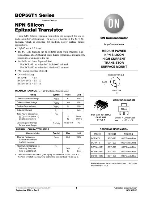
Preferred DevicesThese <strong>NPN</strong> <strong>Silicon</strong> <strong>Epitaxial</strong> transistors are designed for use inaudio amplifier applications. The device is housed in the SOT-223package, which is designed for medium power surface mountapplications.• High Current: 1.0 Amp• The SOT-223 package can be soldered using wave or reflow. Theformed leads absorb thermal stress during soldering, eliminating thepossibility of damage to the die• Available in 12 mm Tape and ReelUse <strong>BCP56T1</strong> to order the 7 inch/1000 unit reelUse BCP56T3 to order the 13 inch/4000 unit reel• PNP Complement is BCP53T1• Device Marking<strong>BCP56T1</strong>–10 = BHBCP56–10T1 = BH–10BCP56–16T1 = BH–16MAXIMUM RATINGS (TC = 25°C unless otherwise noted)Rating Symbol Value UnitCollector-Emitter Voltage VCEO 80 VdcCollector-Base Voltage VCBO 100 VdcEmitter-Base Voltage VEBO 5 VdcCollector Current IC 1 AdcTotal Power Dissipation@ TA = 25°C (Note 1.)Derate above 25°COperating and StorageTemperature RangeTHERMAL CHARACTERISTICSPD1.512WattsmW/°CTJ, Tstg –65 to 150 °CCharacteristic Symbol Max UnitThermal ResistanceJunction-to-Ambient(surface mounted)Maximum Temperature forSoldering PurposesTime in Solder BathRθJA 83.3 °C/WTL260101. Device mounted on a FR-4 glass epoxy printed circuit board 1.575 in. x1.575 in. x 0.0625 in.; mounting pad for the collector lead = 0.93 sq. in.°CSecSOT–223, TO–261AACASE 318ESTYLE 1http://onsemi.comMEDIUM POWER<strong>NPN</strong> SILICONHIGH CURRENTTRANSISTORSURFACE MOUNTBASE11234COLLECTOR 2,4EMITTER3MARKING DIAGRAMBHxxxBHxxx = Device Codexxx = –10 or –16ORDERING INFORMATIONDevice Package Shipping<strong>BCP56T1</strong> SOT–223 1000/Tape & ReelBCP56T3 SOT–223 4000/Tape & ReelBCP56–10T1 SOT–223 1000/Tape & ReelBCP56–16T1 SOT–223 1000/Tape & ReelBCP56–16T3 SOT–223 4000/Tape & ReelPreferred devices are recommended choices for future useand best overall value.© Semiconductor Components Industries, LLC, 2001September, 2000 – Rev. 21 Publication Order Number:<strong>BCP56T1</strong>/D
<strong>BCP56T1</strong> <strong>Series</strong>ELECTRICAL CHARACTERISTICS (TA = 25°C unless otherwise noted)Characteristics Symbol Min Typ Max UnitOFF CHARACTERISTICSCollector-Base Breakdown VoltageV(BR)CBO 100 – – Vdc(IC = 100 µAdc, IE = 0)Collector-Emitter Breakdown Voltage(IC = 1.0 mAdc, IB = 0)Emitter-Base Breakdown Voltage(IE = 10 µAdc, IC = 0)Collector-Base Cutoff Current(VCB = 30 Vdc, IE = 0)Emitter-Base Cutoff Current(VEB = 5.0 Vdc, IC = 0)ON CHARACTERISTICS (Note 2.)DC Current Gain(IC = 5.0 mA, VCE = 2.0 V)(IC = 150 mA, VCE = 2.0 V)(IC = 500 mA, VCE = 2.0 V)Collector-Emitter Saturation Voltage(IC = 500 mAdc, IB = 50 mAdc)Base-Emitter On Voltage(IC = 500 mAdc, VCE = 2.0 Vdc)All Part Types<strong>BCP56T1</strong>BCP56-10T1BCP56-16T1All TypesV(BR)CEO 80 – – VdcV(BR)EBO 5.0 – – VdcICBO – – 100 nAdcIEBO – – 10 µAdchFE25406310025––––––250160250–VCE(sat) – – 0.5 VdcVBE(on) – – 1.0 Vdc–DYNAMIC CHARACTERISTICSCurrent-Gain – Bandwidth Product(IC = 10 mAdc, VCE = 5.0 Vdc, f = 35 MHz)2. Pulse Test: Pulse Width ≤ 300 µs, Duty Cycle ≤ 2.0%fT – 130 – MHzhttp://onsemi.com2
<strong>BCP56T1</strong> <strong>Series</strong>TYPICAL ELECTRICAL CHARACTERISTICS°°°Figure 1. DC Current Gain° Figure 2. Current-Gain – Bandwidth ProductFigure 3. Capacitance° °Figure 4. “On” VoltagesFigure 5. Collector Saturation Regionhttp://onsemi.com3
<strong>BCP56T1</strong> <strong>Series</strong>INFORMATION FOR USING THE SOT–223 SURFACE MOUNT PACKAGEMINIMUM RECOMMENDED FOOTPRINT FOR SURFACE MOUNTED APPLICATIONSSurface mount board layout is a critical portion of the totaldesign. The footprint for the semiconductor packages mustbe the correct size to insure proper solder connectioninterface between the board and the package. With thecorrect pad geometry, the packages will self align whensubjected to a solder reflow process.SOT–223mminchesSOT–223 POWER DISSIPATIONThe power dissipation of the SOT–223 is a function ofthe pad size. This can vary from the minimum pad size forsoldering to the pad size given for maximum power dissipation.Power dissipation for a surface mount device is determinedby TJ(max), the maximum rated junction temperatureof the die, RθJA, the thermal resistance from the devicejunction to ambient; and the operating temperature, TA. Usingthe values provided on the data sheet for the SOT–223package, PD can be calculated as follows.PD =PD =150°C – 25°C83.3°C/WTJ(max) – TARθJAThe values for the equation are found in the maximumratings table on the data sheet. Substituting these values intothe equation for an ambient temperature TA of 25°C, onecan calculate the power dissipation of the device which inthis case is 1.5 watts.= 1.50 wattsThe 83.3°C/W for the SOT-223 package assumes theuse of the recommended footprint on a glass epoxyprinted circuit board to achieve a power dissipation of 1.5watts. There are other alternatives to achieving higherpower dissipation from the SOT-223 package. One is toincrease the area of the collector pad. By increasing thearea of the collector pad, the power dissipation can beincreased. Although the power dissipation can almost beθdoubled with this method, area is taken up on the printedcircuit board which can defeat the purpose of usingsurface mount technology. A graph of RθJA versus collectorpad area is shown in Figure 6.° ″° Figure 6. Thermal Resistance versus CollectorPad Area for the SOT-223 Package (Typical)Another alternative would be to use a ceramic substrateor an aluminum core board such as Thermal Clad. Usinga board material such as Thermal Clad, an aluminum coreboard, the power dissipation can be doubled using the samefootprint.http://onsemi.com4
<strong>BCP56T1</strong> <strong>Series</strong>SOLDER STENCIL GUIDELINESPrior to placing surface mount components onto a printedcircuit board, solder paste must be applied to the pads. Asolder stencil is required to screen the optimum amount ofsolder paste onto the footprint. The stencil is made of brassor stainless steel with a typical thickness of 0.008 inches.The stencil opening size for the surface mounted packageshould be the same as the pad size on the printed circuitboard, i.e., a 1:1 registration.SOLDERING PRECAUTIONSThe melting temperature of solder is higher than the ratedtemperature of the device. When the entire device is heatedto a high temperature, failure to complete soldering withina short time could result in device failure. Therefore, thefollowing items should always be observed in order tominimize the thermal stress to which the devices aresubjected.• Always preheat the device.• The delta temperature between the preheat andsoldering should be 100°C or less.*• When preheating and soldering, the temperature of theleads and the case must not exceed the maximumtemperature ratings as shown on the data sheet. Whenusing infrared heating with the reflow solderingmethod, the difference should be a maximum of 10°C.• The soldering temperature and time should not exceed260°C for more than 10 seconds.• When shifting from preheating to soldering, themaximum temperature gradient should be 5°C or less.• After soldering has been completed, the device shouldbe allowed to cool naturally for at least three minutes.Gradual cooling should be used as the use of forcedcooling will increase the temperature gradient andresult in latent failure due to mechanical stress.• Mechanical stress or shock should not be applied duringcooling* Soldering a device without preheating can cause excessivethermal shock and stress which can result in damageto the device.For any given circuit board, there will be a group ofcontrol settings that will give the desired heat pattern. Theoperator must set temperatures for several heating zones,and a figure for belt speed. Taken together, these controlsettings make up a heating “profile” for that particularcircuit board. On machines controlled by a computer, thecomputer remembers these profiles from one operatingsession to the next. Figure 7 shows a typical heating profilefor use when soldering a surface mount device to a printedcircuit board. This profile will vary among solderingsystems but it is a good starting point. Factors that canaffect the profile include the type of soldering system inuse, density and types of components on the board, type ofsolder used, and the type of board or substrate materialbeing used. This profile shows temperature versus time.TYPICAL SOLDER HEATING PROFILEThe line on the graph shows the actual temperature thatmight be experienced on the surface of a test board at ornear a central solder joint. The two profiles are based on ahigh density and a low density board. The VitronicsSMD310 convection/infrared reflow soldering system wasused to generate this profile. The type of solder used was62/36/2 Tin Lead Silver with a melting point between177–189°C. When this type of furnace is used for solderreflow work, the circuit boards and solder joints tend toheat first. The components on the board are then heated byconduction. The circuit board, because it has a large surfacearea, absorbs the thermal energy more efficiently, thendistributes this energy to the components. Because of thiseffect, the main body of a component may be up to 30degrees cooler than the adjacent solder joints.http://onsemi.com5
<strong>BCP56T1</strong> <strong>Series</strong>°°°°°°°°°°°Figure 7. Typical Solder Heating Profilehttp://onsemi.com6
<strong>BCP56T1</strong> <strong>Series</strong>PACKAGE DIMENSIONSLSHGAF DBCSOT–223(TO–261AA)PLASTIC PACKAGECASE 318E–04ISSUE HMKJ http://onsemi.com7
<strong>BCP56T1</strong> <strong>Series</strong>Thermal Clad is a trademark of the Bergquist Company.ON Semiconductor and are trademarks of Semiconductor Components Industries, LLC (SCILLC). SCILLC reserves the right to make changeswithout further notice to any products herein. SCILLC makes no warranty, representation or guarantee regarding the suitability of its products for any particularpurpose, nor does SCILLC assume any liability arising out of the application or use of any product or circuit, and specifically disclaims any and all liability,including without limitation special, consequential or incidental damages. “Typical” parameters which may be provided in SCILLC data sheets and/orspecifications can and do vary in different applications and actual performance may vary over time. All operating parameters, including “Typicals” must bevalidated for each customer application by customer’s technical experts. SCILLC does not convey any license under its patent rights nor the rights of others.SCILLC products are not designed, intended, or authorized for use as components in systems intended for surgical implant into the body, or other applicationsintended to support or sustain life, or for any other application in which the failure of the SCILLC product could create a situation where personal injury ordeath may occur. Should Buyer purchase or use SCILLC products for any such unintended or unauthorized application, Buyer shall indemnify and holdSCILLC and its officers, employees, subsidiaries, affiliates, and distributors harmless against all claims, costs, damages, and expenses, and reasonableattorney fees arising out of, directly or indirectly, any claim of personal injury or death associated with such unintended or unauthorized use, even if such claimalleges that SCILLC was negligent regarding the design or manufacture of the part. SCILLC is an Equal Opportunity/Affirmative Action Employer.PUBLICATION ORDERING INFORMATIONLiterature Fulfillment:Literature Distribution Center for ON SemiconductorP.O. Box 5163, Denver, Colorado 80217 USAPhone: 303–675–2175 or 800–344–3860 Toll Free USA/CanadaFax: 303–675–2176 or 800–344–3867 Toll Free USA/CanadaEmail: ONlit@hibbertco.comN. American Technical Support: 800–282–9855 Toll Free USA/CanadaJAPAN: ON Semiconductor, Japan Customer Focus Center4–32–1 Nishi–Gotanda, Shinagawa–ku, Tokyo, Japan 141–0031Phone: 81–3–5740–2700Email: r14525@onsemi.comON Semiconductor Website: http://onsemi.comFor additional information, please contact your localSales Representative.http://onsemi.com8<strong>BCP56T1</strong>/D
This datasheet has been download from:www.datasheetcatalog.com<strong>Datasheet</strong>s for electronics components.


