

MCP3421 - Microchip
MCP3421 - Microchip
MCP3421 - Microchip

You also want an ePaper? Increase the reach of your titles
YUMPU automatically turns print PDFs into web optimized ePapers that Google loves.
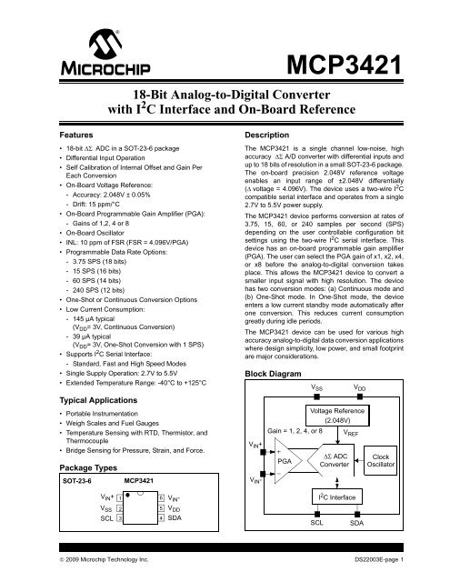
<strong>MCP3421</strong>18-Bit Analog-to-Digital Converterwith I 2 C Interface and On-Board ReferenceFeatures• 18-bit ΔΣ ADC in a SOT-23-6 package• Differential Input Operation• Self Calibration of Internal Offset and Gain PerEach Conversion• On-Board Voltage Reference:- Accuracy: 2.048V ± 0.05%- Drift: 15 ppm/°C• On-Board Programmable Gain Amplifier (PGA):- Gains of 1,2, 4 or 8• On-Board Oscillator• INL: 10 ppm of FSR (FSR = 4.096V/PGA)• Programmable Data Rate Options:- 3.75 SPS (18 bits)- 15 SPS (16 bits)- 60 SPS (14 bits)- 240 SPS (12 bits)• One-Shot or Continuous Conversion Options• Low Current Consumption:- 145 µA typical(V DD = 3V, Continuous Conversion)- 39 µA typical(V DD = 3V, One-Shot Conversion with 1 SPS)• Supports I 2 C Serial Interface:- Standard, Fast and High Speed Modes• Single Supply Operation: 2.7V to 5.5V• Extended Temperature Range: -40°C to +125°CTypical Applications• Portable Instrumentation• Weigh Scales and Fuel Gauges• Temperature Sensing with RTD, Thermistor, andThermocouple• Bridge Sensing for Pressure, Strain, and Force.Package TypesSOT-23-6<strong>MCP3421</strong>DescriptionThe <strong>MCP3421</strong> is a single channel low-noise, highaccuracy ΔΣ A/D converter with differential inputs andup to 18 bits of resolution in a small SOT-23-6 package.The on-board precision 2.048V reference voltageenables an input range of ±2.048V differentially(Δ voltage = 4.096V). The device uses a two-wire I 2 Ccompatible serial interface and operates from a single2.7V to 5.5V power supply.The <strong>MCP3421</strong> device performs conversion at rates of3.75, 15, 60, or 240 samples per second (SPS)depending on the user controllable configuration bitsettings using the two-wire I 2 C serial interface. Thisdevice has an on-board programmable gain amplifier(PGA). The user can select the PGA gain of x1, x2, x4,or x8 before the analog-to-digital conversion takesplace. This allows the <strong>MCP3421</strong> device to convert asmaller input signal with high resolution. The devicehas two conversion modes: (a) Continuous mode and(b) One-Shot mode. In One-Shot mode, the deviceenters a low current standby mode automatically afterone conversion. This reduces current consumptiongreatly during idle periods.The <strong>MCP3421</strong> device can be used for various highaccuracy analog-to-digital data conversion applicationswhere design simplicity, low power, and small footprintare major considerations.Block DiagramV IN +V IN -V SSGain = 1, 2, 4, or 8PGAV DDVoltage Reference(2.048V)ΔΣ ADCConverterV REFClockOscillatorV IN +V IN -I 2 C InterfaceV SSSCL16253 4V DDSDASCLSDA© 2009 <strong>Microchip</strong> Technology Inc. DS22003E-page 1
<strong>MCP3421</strong>NOTES:DS22003E-page 2© 2009 <strong>Microchip</strong> Technology Inc.
<strong>MCP3421</strong>1.0 ELECTRICALCHARACTERISTICS1.1 Absolute Maximum Ratings†V DD ...................................................................................7.0VAll inputs and outputs w.r.t V SS ............... –0.3V to V DD +0.3VDifferential Input Voltage ...................................... |V DD - V SS |Output Short Circuit Current ................................ContinuousCurrent at Input Pins ....................................................±2 mACurrent at Output and Supply Pins ............................±10 mAStorage Temperature ....................................-65°C to +150°CAmbient Temp. with power applied ...............-55°C to +125°CESD protection on all pins ................ ≥ 6kVHBM, ≥ 400V MMMaximum Junction Temperature (T J ). .........................+150°C†Notice: Stresses above those listed under “Maximum Ratings”may cause permanent damage to the device. This is astress rating only and functional operation of the device atthose or any other conditions above those indicated in theoperational listings of this specification is not implied.Exposure to maximum rating conditions for extended periodsmay affect device reliability.1.2 Electrical SpecificationsELECTRICAL CHARACTERISTICSElectrical Specifications: Unless otherwise specified, all parameters apply for T A = -40°C to +85°C, V DD = +5.0V, V SS = 0V,V IN + = V IN - = V REF /2. All ppm units use 2*V REF as full scale range.Parameters Sym Min Typ Max Units ConditionsAnalog InputsDifferential Input Range — ±2.048/PGA — V V IN = V IN + - V IN -Common-Mode Voltage RangeV SS -0.3 — V DD +0.3 V(absolute) (Note 1)Differential Input Impedance Z IND (f) — 2.25/PGA — MΩ During normal mode operation(Note 2)Common Mode inputZ INC (f) — 25 — MΩ PGA = 1, 2, 4, 8ImpedanceSystem PerformanceResolution and No Missing12 — — Bits DR = 240 SPSCodes (Note 8)14 — — Bits DR = 60 SPS16 — — Bits DR = 15 SPS18 — — Bits DR = 3.75 SPSData Rate (Note 3) DR 176 240 328 SPS S1,S0 = ‘00’, (12 bits mode)44 60 82 SPS S1,S0 = ‘01’, (14 bits mode)11 15 20.5 SPS S1,S0 = ‘10’, (16 bits mode)2.75 3.75 5.1 SPS S1,S0 = ‘11’, (18 bits mode)Output Noise — 1.5 — µV RMS T A = +25°C, DR = 3.75 SPS,PGA = 1, V IN = 0Integral Nonlinearity (Note 4) INL — 10 35 ppm ofFSRInternal Reference Voltage V REF — 2.048 — VDR = 3.75 SPS(Note 6)Note 1: Any input voltage below or greater than this voltage causes leakage current through the ESD diodes at the input pins.This parameter is ensured by characterization and not 100% tested.2: This input impedance is due to 3.2 pF internal input sampling capacitor.3: The total conversion speed includes auto-calibration of offset and gain.4: INL is the difference between the endpoints line and the measured code at the center of the quantization band.5: Includes all errors from on-board PGA and V REF .6: Full Scale Range (FSR) = 2 x 2.048/PGA = 4.096/PGA.7: This parameter is ensured by characterization and not 100% tested.8: This parameter is ensured by design and not 100% tested.© 2009 <strong>Microchip</strong> Technology Inc. DS22003E-page 3
<strong>MCP3421</strong>ELECTRICAL CHARACTERISTICS (CONTINUED)Electrical Specifications: Unless otherwise specified, all parameters apply for T A = -40°C to +85°C, V DD = +5.0V, V SS = 0V,V IN + = V IN - = V REF /2. All ppm units use 2*V REF as full scale range.Parameters Sym Min Typ Max Units ConditionsGain Error (Note 5) — 0.05 0.35 % PGA = 1, DR = 3.75 SPSPGA Gain Error Match (Note 5) — 0.1 — % Between any 2 PGA gainsGain Error Drift (Note 5) — 15 — ppm/°C PGA=1, DR=3.75 SPSOffset Error V OS — 15 40 µV Tested at PGA = 1V DD = 5.0V and DR = 3.75 SPSOffset Drift vs. Temperature — 50 — nV/°C V DD = 5.0VCommon-Mode Rejection — 105 — dB at DC and PGA =1,— 110 — dB at DC and PGA =8,T A = +25°CGain vs. V DD — 5 — ppm/V T A = +25°C, V DD = 2.7V to 5.5V,PGA = 1Power Supply Rejection at DC — 100 — dB T A = +25°C, V DD = 2.7V to 5.5V,PGA = 1Power RequirementsVoltage Range V DD 2.7 — 5.5 VSupply Current duringI DDA — 155 190 µA V DD = 5.0VConversion— 145 — µA V DD = 3.0VSupply Current during Standby I DDS — 0.1 0.5 µAModeI 2 C Digital Inputs and Digital OutputsHigh level input voltage V IH 0.7 V DD — V DD VLow level input voltage V IL — — 0.3V DD VLow level output voltage V OL — — 0.4 V I OL = 3 mA, V DD = +5.0VHysteresis of Schmitt Trigger V HYST 0.05V DD — — V f SCL = 100 kHzfor inputs (Note 7)Supply Current when I 2 C bus I DDB — — 10 µAline is activeInput Leakage Current I ILH — — 1 µA V IH = 5.5VI ILL -1 — — µA V IL = GNDPin Capacitance and I 2 C Bus CapacitancePin capacitance C PIN — — 10 pFI 2 C Bus Capacitance C b — — 400 pFNote 1: Any input voltage below or greater than this voltage causes leakage current through the ESD diodes at the input pins.This parameter is ensured by characterization and not 100% tested.2: This input impedance is due to 3.2 pF internal input sampling capacitor.3: The total conversion speed includes auto-calibration of offset and gain.4: INL is the difference between the endpoints line and the measured code at the center of the quantization band.5: Includes all errors from on-board PGA and V REF .6: Full Scale Range (FSR) = 2 x 2.048/PGA = 4.096/PGA.7: This parameter is ensured by characterization and not 100% tested.8: This parameter is ensured by design and not 100% tested.DS22003E-page 4© 2009 <strong>Microchip</strong> Technology Inc.
<strong>MCP3421</strong>TEMPERATURE SPECIFICATIONSElectrical Characteristics: Unless otherwise indicated, T A = -40°C to +85°C, V DD = +5.0V, V SS = 0V.Parameters Sym Min Typ Max Units ConditionsTemperature RangesSpecified Temperature Range T A -40 — +85 °COperating Temperature Range T A -40 — +125 °CStorage Temperature Range T A -65 — +150 °CThermal Package ResistancesThermal Resistance, 6L SOT-23 θ JA — 190.5 — °C/W© 2009 <strong>Microchip</strong> Technology Inc. DS22003E-page 5
<strong>MCP3421</strong>NOTES:DS22003E-page 6© 2009 <strong>Microchip</strong> Technology Inc.
<strong>MCP3421</strong>2.0 TYPICAL PERFORMANCE CURVESNote:The graphs and tables provided following this note are a statistical summary based on a limited number ofsamples and are provided for informational purposes only. The performance characteristics listed hereinare not tested or guaranteed. In some graphs or tables, the data presented may be outside the specifiedoperating range (e.g., outside specified power supply range) and therefore outside the warranted range.Note: Unless otherwise indicated, T A = -40°C to +85°C, V DD = +5.0V, V SS = 0V, V IN + = V IN - = V REF /2.Integral Nonlinearity (% of FSR).005.004.003.002.001.000PGA = 8PGA = 2PGA = 4PGA = 12.5 3 3.5 4 4.5 5 5.5V DD (V)Noise (µV, rms)10.07.55.02.5T A = +25°CV DD = 5VPGA = 1PGA = 2PGA = 4PGA = 80.0-100 -75 -50 -25 0 25 50 75 100Input Voltage (% of Full Scale)FIGURE 2-1:(V DD ).INL vs. Supply VoltageFIGURE 2-4:Voltage.Output Noise vs. InputIntegral Nonlinearity(% of FSR)0.0030.0020.001PGA = 1V DD = 5 VV DD = 2.7V0-60 -40 -20 0 20 40 60 80 100 120 140Temperature ( o C)Total Error (mV)3.0PGA = 12.0PGA = 2PGA = 41.0PGA = 80.0-1.0-2.0-3.0-100 -75 -50 -25 0 25 50 75 100Input Voltage (% of Full Scale)FIGURE 2-2:INL vs. Temperature.FIGURE 2-5:Total Error vs. Input Voltage.Offset Error (µV)20V DD = 5V15PGA = 410PGA = 8PGA = 250-5PGA = 1-10-15-20-60 -40 -20 0 20 40 60 80 100 120 140Temperature (°C)Gain Error (% of FSR)0.4V DD = 5.0V0.30.2PGA = 10.1PGA = 20-0.1-0.2-0.3PGA = 4-0.4PGA = 8-60 -40 -20 0 20 40 60 80 100 120 140Temperature (°C)FIGURE 2-3:Temperature.Offset Error vs.FIGURE 2-6:Gain Error vs. Temperature.© 2009 <strong>Microchip</strong> Technology Inc. DS22003E-page 7
<strong>MCP3421</strong>Note: Unless otherwise indicated, T A = -40°C to +85°C, V DD = +5.0V, V SS = 0V, V IN + = V IN - = V REF /2.I DDA (µA)220200VDD = 5V180160140V DD = 2.7V120100-60 -40 -20 0 20 40 60 80 100 120 140Temperature ( o C)FIGURE 2-7: I DDA vs. Temperature.Oscillator Drift (%)5432V DD = 2.7V10 V DD = 5.0V-1-60 -40 -20 0 20 40 60 80 100 120 140Temperature (°C)FIGURE 2-10: OSC Drift vs. Temperature.I DDS (nA)600500400300200V DD = 5V100V DD = 2.7V0-60 -40 -20 0 20 40 60 80 100 120 140Temperature ( o C)Magnitude (dB)0-10Data Rate = 3.75 SPS-20-30-40-50-60-70-80-90-100-110-1200.1 1 10 10010001k1000010kInput Signal Frequency (Hz)FIGURE 2-8:I DDS vs. Temperature.FIGURE 2-11:Frequency Response.I DDB (μA)98 V DD = 5V7VDD = 4.5V65VDD = 3.3V43VDD = 2.7V210-60 -40 -20 0 20 40 60 80 100 120 140Temperature ( o C)FIGURE 2-9: I DDB vs. Temperature.DS22003E-page 8© 2009 <strong>Microchip</strong> Technology Inc.
<strong>MCP3421</strong>3.4 Serial Data Pin (SDA)SDA is the serial data pin of the I 2 C interface. The SDApin is used for input and output data. In read mode, theconversion result is read from the SDA pin (output). Inwrite mode, the device configuration bits are written(input) though the SDA pin. The SDA pin is an opendrainN-channel driver. Therefore, it needs a pull-upresistor from the V DD line to the SDA pin. Except forstart and stop conditions, the data on the SDA pin mustbe stable during the high period of the clock. The highor low state of the SDA pin can only change when theclock signal on the SCL pin is low. Refer to Section 5.3“I 2 C Serial Communications” for more details of I 2 CSerial Interface communication.Typical range of the pull-up resistor value for SCL andSDA is from 5 kΩ to 10 kΩ for standard (100 kHz) andfast (400 kHz) modes, and less than 1 kΩ for highspeed mode (3.4 MHz). The High-Speed mode is notrecommended for V DD less than 2.7V.R SSV IN +,V IN -D 1V DDV T = 0.6VSamplingSwitchVC PIN4pFD 2V T = 0.6VI LEAKAGE(~ ±1 nA)SS R SC SAMPLE(3.2 pF)V SSLegend:V = Signal Source I LEAKAGE = Leakage Current at Analog PinR SS = Source Impedance SS = Sampling SwitchV IN +, V IN - = Analog Input Pin R S = Sampling Switch ResistorC PIN = Input Pin Capacitance C SAMPLE = Sample CapacitanceV T = Threshold Voltage D 1 , D 2 = ESD Protection DiodeFIGURE 3-1:Equivalent Analog Input Circuit.DS22003E-page 10© 2009 <strong>Microchip</strong> Technology Inc.
<strong>MCP3421</strong>4.0 DESCRIPTION OF DEVICEOPERATION4.1 General OverviewThe <strong>MCP3421</strong> is a low-power, 18-Bit Delta-Sigma A/Dconverter with an I 2 C serial interface. The devicecontains an on-board voltage reference (2.048V),programmable gain amplifier (PGA), and internaloscillator. When the device powers up (POR is set), itautomatically resets the configuration bits to defaultsettings.Device default settings are:• Conversion bit resolution: 12 bits (240 sps)• PGA gain setting: x1• Continuous conversionOnce the device is powered-up, the user canreprogram the configuration bits using I 2 C serialinterface any time. The configuration bits are stored involatile memory.User selectable options are:• Conversion bit resolution: 12, 14, 16, or 18 bits• PGA Gain selection: x1, x2, x4, or x8• Continuous or one-shot conversionIn the Continuous Conversion mode, the deviceconverts the inputs continuously. While in the One-ShotConversion mode, the device converts the input onetime and stays in the low-power standby mode until itreceives another command for a new conversion.During the standby mode, the device consumes lessthan 1 µA maximum.4.2 Power-On-Reset (POR)The device contains an internal Power-On-Reset(POR) circuit that monitors power supply voltage (V DD )during operation. This circuit ensures correct devicestart-up at system power-up and power-down events.The POR has built-in hysteresis and a timer to give ahigh degree of immunity to potential ripples and noiseson the power supply. A 0.1 µF decoupling capacitorshould be mounted as close as possible to the V DD pinfor additional transient immunity.The threshold voltage is set at 2.2V with a tolerance ofapproximately ±5%. If the supply voltage falls belowthis threshold, the device will be held in a resetcondition. The typical hysteresis value is approximately200 mV.The POR circuit is shut-down during the low-powerstandby mode. Once a power-up event has occurred,the device requires additional delay time(approximately 300 µs) before a conversion can takeplace. During this time, all internal analog circuitries aresettled before the first conversion occurs. Figure 4-1illustrates the conditions for power-up and power-downevents under typical start-up conditions.When the device powers up, it automatically resetsand sets the configuration bits to default settings. Thedefault configuration bit conditions are a PGA gain of1 V/V and a conversion speed of 240 SPS inContinuous Conversion mode. When the devicereceives an I 2 C General Call Reset command, itperforms an internal reset similar to a Power-On-Resetevent.V DD2.2V2.0VFIGURE 4-1:300 µSReset Start-up Normal Operation ResetPOR Operation.4.3 Internal Voltage ReferenceThe device contains an on-board 2.048V voltagereference. This reference voltage is for internal useonly and not directly measurable. The specifications ofthe reference voltage are part of the device’s gain anddrift specifications. Therefore, there is no separatespecification for the on-board reference.4.4 Analog Input ChannelTimeThe differential analog input channel has a switchedcapacitor structure. The internal sampling capacitor(3.2 pF for PGA = 1) is charged and discharged toprocess a conversion. The charging and discharging ofthe input sampling capacitor creates dynamic inputcurrents at each input pin. The current is a function ofthe differential input voltages, and inverselyproportional to the internal sampling capacitance,sampling frequency, and PGA setting.© 2009 <strong>Microchip</strong> Technology Inc. DS22003E-page 11
<strong>MCP3421</strong>4.5 Input Voltage RangeThe differential (V IN ) and common mode voltage(V INCOM ) at the input pins without considering PGAsetting are defined by:V IN= V IN+ – V IN-VV IN+ + V IN-INCOM= ------------------------------2The input signal levels are amplified by the internalprogrammable gain amplifier (PGA) at the front end ofthe ΔΣ modulator.The user needs to consider two conditions for the inputvoltage range: (a) Differential input voltage range and(b) Absolute maximum input voltage range.4.5.1 DIFFERENTIAL INPUT VOLTAGERANGEThe device performs conversions using its internalreference voltage (V REF = 2.048V). Therefore, theabsolute value of the differential input voltage (V IN ),with PGA setting is included, needs to be less than theinternal reference voltage. The device will outputsaturated output codes (all 0s or all 1s except sign bit)if the absolute value of the input voltage (V IN ), withPGA setting is included, is greater than the internalreference voltage (V REF = 2.048V). The input full-scalevoltage range is given by:EQUATION 4-1:– V REF≤ ( V IN• PGA) ≤ ( V REF– 1LSB)Where:V IN = V IN + - V IN -V REF = 2.048VIf the input voltage level is greater than the above limit,the user can use a voltage divider and bring down theinput level within the full-scale range. See Figure 6-7for more details of the input voltage divider circuit.4.5.2 ABSOLUTE MAXIMUM INPUTVOLTAGE RANGEThe input voltage at each input pin must be less thanthe following absolute maximum input voltage limits:• Input voltage < V DD +0.3V• Input voltage > V SS -0.3VAny input voltage outside this range can turn on theinput ESD protection diodes, and result in inputleakage current, causing conversion errors, orpermanently damage the device.Care must be taken in setting the input voltage rangesso that the input voltage does not exceed the absolutemaximum input voltage range.4.6 Input ImpedanceThe device uses a switched-capacitor input stage usinga 3.2 pF sampling capacitor. This capacitor is switched(charged and discharged) at a rate of the samplingfrequency that is generated by on-board clock. Thedifferential input impedance varies with the PGAsettings. The typical differential input impedance duringa normal mode operation is given by:Z IN (f) = 2.25 MΩ/PGASince the sampling capacitor is only switching to theinput pins during a conversion process, the above inputimpedance is only valid during conversion periods. In alow power standby mode, the above impedance is notpresented at the input pins. Therefore, only a leakagecurrent due to ESD diode is presented at the input pins.The conversion accuracy can be affected by the inputsignal source impedance when any external circuit isconnected to the input pins. The source impedanceadds to the internal impedance and directly affects thetime required to charge the internal sampling capacitor.Therefore, a large input source impedance connectedto the input pins can degrade the system performance,such as offset, gain, and Integral Non-Linearity (INL)errors. Ideally, the input source impedance should bezero. This can be achievable by using an operationalamplifier with a closed-loop output impedance of tensof ohms.4.7 Aliasing and Anti-aliasing FilterAliasing occurs when the input signal contains timevaryingsignal components with frequency greater thanhalf the sample rate. In the aliasing conditions, thedevice can output unexpected output codes. Forapplications that are operating in electrical noiseenvironments, the time-varying signal noise or highfrequency interference components can be easilyadded to the input signals and cause aliasing. Althoughthe device has an internal first order sinc filter, the filterresponse (Figure 2-11) may not give enoughattenuation to all aliasing signal components. To avoidthe aliasing, an external anti-aliasing filter, which canbe accomplished with a simple RC low-pass filter, istypically used at the input pins. The low-pass filter cutsoff the high frequency noise components and providesa band-limited input signal to the input pins.4.8 Self-CalibrationThe device performs a self-calibration of offset andgain for each conversion. This provides reliableconversion results from conversion-to-conversion overvariations in temperature as well as power supplyfluctuations.DS22003E-page 12© 2009 <strong>Microchip</strong> Technology Inc.
<strong>MCP3421</strong>4.9 Digital Output Codes andConversion to Real Values4.9.1 DIGITAL OUTPUT CODE FROMDEVICEThe digital output code is proportional to the inputvoltage and PGA settings. The output data format is abinary two’s complement. With this code scheme, theMSB can be considered a sign indicator. When theMSB is a logic ‘0’, the input is positive. When the MSBis a logic ‘1’, the input is negative. The following is anexample of the output code:a. for a negative full scale input voltage:100...000Example: (V IN +-V IN -) •PGA = -2.048Vb. for a zero differential input voltage: 000...000Example: (V IN +-V IN -) = 0c. for a positive full scale input voltage:011...111Example: (V IN +-V IN -) • PGA = 2.048VThe MSB (sign bit) is always transmitted first throughthe I 2 C serial data line. The resolution for eachconversion is 18, 16, 14, or 12 bits depending on theconversion rate selection bit settings by the user.The output codes will not roll-over even if the input voltageexceeds the maximum input range. In this case,the code will be locked at 0111...11 for all voltagesgreater than (V REF - 1 LSB)/PGA and 1000...00 forvoltages less than -V REF /PGA. Table 4-2 shows anexample of output codes of various input levels for 18bit conversion mode. Table 4-3 shows an example ofminimum and maximum output codes for eachconversion rate option.The number of output code is given by:EQUATION 4-2:Number of Output Code( V IN+ – V IN-)= ( Maximum Code + 1) × PGA × ----------------------------------2.048VWhere:See Table 4-3 for Maximum Code.The LSB of the data conversion is given by:EQUATION 4-3:LSB =2 × V--------------------- REF= --------------------------2 × 2.048VWhere:2 N2 NN = User programmable bit resolution:12,14,16, or 18Table 4-1 shows the LSB size of each conversion ratesetting. The measured unknown input voltage isobtained by multiplying the output codes with LSB. Seethe following section for the input voltage calculationusing the output codes.TABLE 4-1:TABLE 4-2:TABLE 4-3:RESOLUTION SETTINGS VS.LSBResolution SettingLSB12 bits 1 mV14 bits 250 µV16 bits 62.5 µV18 bits 15.625 µVInput Voltage:[V IN +-V IN -] • PGAEXAMPLE OF OUTPUT CODEFOR 18 BITS (NOTE 1,NOTE 2)Digital Output Code≥ V REF 011111111111111111V REF - 1 LSB 0111111111111111112LSB 0000000000000000101LSB 0000000000000000010 000000000000000000-1 LSB 111111111111111111-2 LSB 111111111111111110- V REF 100000000000000000< -V REF 100000000000000000Note 1: MSB is a sign indicator:0: Positive input (V IN +>V IN -)1: Negative input (V IN +
<strong>MCP3421</strong>4.9.2 CONVERTING THE DEVICEOUTPUT CODE TO INPUT SIGNALVOLTAGEWhen the user gets the digital output codes from thedevice as described in Section 4.9.1 “Digital outputcode from device”, the next step is converting thedigital output codes to a measured input voltage.Equation 4-4 shows an example of converting theoutput codes to its corresponding input voltage.If the sign indicator bit (MSB) is ‘0’, the input voltageis obtained by multiplying the output code with the LSBand divided by the PGA setting.If the sign indicator bit (MSB) is ‘1’, the output codeneeds to be converted to two’s complement beforemultiplied by LSB and divided by the PGA setting.Table 4-4 shows an example of converting the deviceoutput codes to input voltage.EQUATION 4-4:Where:CONVERTING OUTPUTCODES TO INPUTVOLTAGEIf MSB = 0 (Positive Output Code):LSBInput Voltage = (Output Code) • -----------PGAIf MSB = 1 (Negative Output Code):LSBInput Voltage = (2′s complement of Output Code) • -----------PGALSB = See Table 4-12’s complement = 1’s complement + 1TABLE 4-4:Input Voltage[V IN +-V IN -] • PGA]EXAMPLE OF CONVERTING OUTPUT CODE TO VOLTAGE (WITH 18 BIT SETTING)Digital Output CodeMSB(sign bit)Example of Converting Output Codes to Input Voltage≥ V REF 011111111111111111 0 (2 16 +2 15 +2 14 +2 13 +2 12 +2 11 +2 10 +2 9 +2 8 +2 7 +2 6 +2 5 +2 4 +2 3 +2 2 +2 1 +2 0 )x LSB(15.625μV)/PGA = 2.048 (V) for PGA = 1V REF - 1 LSB 011111111111111111 0 (2 16 +2 15 +2 14 +2 13 +2 12 +2 11 +2 10 +2 9 +2 8 +2 7 +2 6 +2 5 +2 4 +2 3 +2 2 +2 1 +2 0 )x LSB(15.625μV)/PGA = 2.048 (V) for PGA = 12LSB 000000000000000010 0 (0+0+0+0+0+0+0+0+0+0+0+0+0+0+0+2 1 +0)xLSB(15.625μV)/PGA = 31.25 (μV) for PGA = 11LSB 000000000000000001 0 (0+0+0+0+0+0+0+0+0+0+0+0+0+0+0+0+2 0 )xLSB(15.625μV)/PGA = 15.625 (μV)for PGA = 10 000000000000000000 0 (0+0+0+0+0+0+0+0+0+0+0+0+0+0+0+0+0)xLSB(15.625μV)/PGA = 0 V (V) for PGA = 1-1 LSB 111111111111111111 1 -(0+0+0+0+0+0+0+0+0+0+0+0+0+0+0+0+2 0 )xLSB(15.625μV)/PGA = - 15.625 (μV)for PGA = 1-2 LSB 111111111111111110 1 -(0+0+0+0+0+0+0+0+0+0+0+0+0+0+0+2 1 +0)xLSB(15.625μV)/PGA = - 31.25 (μV)for PGA = 1- V REF 100000000000000000 1 -(2 17 +0+0+0+0+0+0+0+0+0+0+0+0+0+0+0+0+0) xLSB(15.625μV)/PGA = - 2.048 (V) for PGA = 1≤ -V REF 100000000000000000 1 -(2 17 +0+0+0+0+0+0+0+0+0+0+0+0+0+0+0+0+0) xLSB(15.625μV)/PGA = - 2.048 (V) for PGA = 1DS22003E-page 14© 2009 <strong>Microchip</strong> Technology Inc.
<strong>MCP3421</strong>5.0 USING THE <strong>MCP3421</strong> DEVICE5.1 Operating ModesThe user operates the device by setting up the deviceconfiguration register using a write command (seeFigure 5-2) and reads the conversion data using a readcommand (see Figure 5-3 and Figure 5-4). The deviceoperates in two modes: (a) Continuous ConversionMode or (b) One-Shot Conversion Mode (singleconversion). This mode selection is made by settingthe O/C bit in the Configuration Register. Refer toSection 5.2 “Configuration Register” for moreinformation.5.1.1 CONTINUOUS CONVERSIONMODE (O/C BIT = 1)The device performs a Continuous Conversion if theO/C bit is set to logic “high”. Once the conversion iscompleted, RDY bit is toggled to ‘0’ and the result isplaced at the output data register. The deviceimmediately begins another conversion and overwritesthe output data register with the most recent result. Thedevice clears the data ready flag (RDY bit = 0) whenthe conversion is completed. The device sets the readyflag bit (RDY bit = 1), if the latest conversion result hasbeen read by the Master.• When writing configuration register:- Setting RDY bit in continuous mode does notaffect anything• When reading conversion data:- RDY bit = 0 means the latest conversionresult is ready- RDY bit = 1 means the conversion result isnot updated since the last reading. A newconversion is under processing and the RDYbit will be cleared when the new conversionresult is ready5.1.2 ONE-SHOT CONVERSION MODE(O/C BIT = 0)Once the One-Shot Conversion (single conversion)Mode is selected, the device performs only oneconversion, updates the output data register, clears thedata ready flag (RDY = 0), and then enters a low powerstandby mode. A new One-Shot Conversion is startedagain when the device receives a new write commandwith RDY = 1.• When writing configuration register:- The RDY bit needs to be set to begin a newconversion in one-shot mode• When reading conversion data:- RDY bit = 0 means the latest conversionresult is ready- RDY bit = 1 means the conversion result isnot updated since the last reading. A newconversion is under processing and the RDYbit will be cleared when the new conversion isdoneThis One-Shot Conversion Mode is highlyrecommended for low power operating applicationswhere the conversion result is needed by request ondemand. During the low current standby mode, thedevice consumes less than 1 µA maximum (or 300 nAtypical). For example, if the user collects 18 bitconversion data once a second in One-ShotConversion mode, the device draws only about onefourth of its total operating current. In this example, thedevice consumes approximately 39 µA (145 µA / 3.75SPS = 39 µA), if the device performs only oneconversion per second (1 SPS) in 18-bit conversionmode with 3V power supply.© 2009 <strong>Microchip</strong> Technology Inc. DS22003E-page 15
<strong>MCP3421</strong>5.2 Configuration RegisterThe device has an 8-bit wide configuration register toselect for: input channel, conversion mode, conversionrate, and PGA gain. This register allows the user tochange the operating condition of the device and checkthe status of the device operation.The user can rewrite the configuration byte any timeduring the device operation. Register 5-1 shows theconfiguration register bits.REGISTER 5-1:CONFIGURATION REGISTERR/W-1 R/W-0 R/W-0 R/W-1 R/W-0 R/W-0 R/W-0 R/W-0RDY C1 C0 O/C S1 S0 G1 G01 * 0 * 0 * 1 * 0 * 0 * 0 * 0 *bit 7 bit 0* Default Configuration after Power-On ResetLegend:R = Readable bit W = Writable bit U = Unimplemented bit, read as ‘0’-n = Value at POR ‘1’ = Bit is set ‘0’ = Bit is cleared x = Bit is unknownbit 7bit 6-5bit 4bit 3-2bit 1-0RDY: Ready BitThis bit is the data ready flag. In read mode, this bit indicates if the output register has been updatedwith a latest conversion result. In One-Shot Conversion mode, writing this bit to “1” initiates a newconversion.Reading RDY bit with the read command:1 = Output register has not been updated.0 = Output register has been updated with the latest conversion result.Writing RDY bit with the write command:Continuous Conversion mode: No effectOne-Shot Conversion mode:1 = Initiate a new conversion.0 = No effect.C1-C0: These bits are not effected for the <strong>MCP3421</strong>.O/C: Conversion Mode Bit1 = Continuous Conversion Mode (Default). The device performs data conversions continuously.0 = One-Shot Conversion Mode. The device performs a single conversion and enters a low powerstandby mode until it receives another write or read command.S1-S0: Sample Rate Selection Bit00 = 240 SPS (12 bits) (Default)01 = 60 SPS (14 bits)10 = 15 SPS (16 bits)11 = 3.75 SPS (18 bits)G1-G0: PGA Gain Selection Bits00 = x1 (Default)01 = x210 = x411 = x8DS22003E-page 16© 2009 <strong>Microchip</strong> Technology Inc.
<strong>MCP3421</strong>If the configuration byte is read repeatedly by clockingcontinuously after reading the data bytes (i.e., after the5th byte in the 18-bit conversion mode), the state of theRDY bit indicates whether the device is ready with newconversion result. When the Master finds the RDY bit iscleared, it can send a not-acknowledge (NAK) bit anda stop bit to exit the current read operation and send anew read command for the latest conversion data.Once the conversion data has been read, the ready bittoggles to ‘1’ until the next new conversion data isready. The conversion data in the output register isoverwritten every time a new conversion is completed.Figure 5-3 and Figure 5-4 show the examples ofreading the conversion data. The user can rewrite theconfiguration byte any time for a new setting.Table 5-1 and Table 5-2 show the examples of theconfiguration bit operation.TABLE 5-1:WRITE CONFIGURATION BITSR/W O/C RDY Operation0 0 0 No effect if all other bits remainthe same - operation continueswith the previous settings0 0 1 Initiate One-Shot Conversion0 1 0 Initiate Continuous Conversion0 1 1 Initiate Continuous ConversionTABLE 5-2: READ CONFIGURATION BITSR/W O/C RDY Operation1 0 0 New conversion result in One-Shot conversion mode has justbeen read. The RDY bit remainslow until set by a new writecommand.1 0 1 One-Shot Conversion is inprogress. The conversion resultis not updated yet. The RDY bitstays high until the currentconversion is completed.1 1 0 New conversion result inContinuous Conversion modehas just been read. The RDY bitchanges to high after reading theconversion data.1 1 1 The conversion result inContinuous Conversion modewas already read. The next newconversion data is not ready. TheRDY bit stays high until a newconversion is completed.5.3 I 2 C Serial CommunicationsThe device communicates with Master(microcontroller) through a serial I 2 C (Inter-IntegratedCircuit) interface and support standard (100 kbits/sec),fast (400 kbits/sec) and high-speed (3.4 Mbits/sec)modes.Note: The High-Speed mode is notrecommended for V DD less than 2.7V.The serial I 2 C is a bidirectional 2-wire data buscommunication protocol using open-drain SCL andSDA lines.The device can only be addressed as a slave. Onceaddressed, it can receive configuration bits with a writecommand or transmit the latest conversion results witha read command. The serial clock pin (SCL) is an inputonly and the serial data pin (SDA) is bidirectional. TheMaster starts communication by sending a START bitand terminates the communication by sending a STOPbit. In read mode, the device releases the SDA lineafter receiving NAK and STOP bits.An example of a hardware connection diagram isshown in Figure 6-1. More details of the I 2 C buscharacteristic is described in Section 5.6 “I 2 C BusCharacteristics”.5.3.1 I 2 C DEVICE ADDRESSINGThe first byte after the START bit is always the addressbyte of the device, which includes the device code(4 bits), address bits (3 bits), and R/W bit. The devicecode of the <strong>MCP3421</strong> is 1101, which is programmed atthe factory. The device code is followed by threeaddress bits (A2, A1, A0) which are also programmedat the factory. The three address bits allow up to eight<strong>MCP3421</strong> devices on the same data bus line.The (R/W) bit determines if the Master device wants toread the conversion data or write to the Configurationregister. If the (R/W) bit is set (read mode), the deviceoutputs the conversion data in the following clocks. Ifthe (R/W) bit is cleared (write mode), the deviceexpects a configuration byte in the following clocks.When the device receives the correct address byte, itoutputs an acknowledge bit after the R/W bit.Figure 5-1 shows the address byte. Figure 5-2 throughFigure 5-4 show how to write the configuration registerbits and read the conversion results.© 2009 <strong>Microchip</strong> Technology Inc. DS22003E-page 17
<strong>MCP3421</strong>Start bitAddressAddress ByteAcknowledge bitRead/Write bitR/W ACKAddressDevice Code Address Bits (Note 1)5.3.2 WRITING A CONFIGURATION BYTETO THE DEVICEWhen the Master sends an address byte with the R/Wbit low (R/W = 0), the <strong>MCP3421</strong> expects oneconfiguration byte following the address. Any byte sentafter this second byte will be ignored. The user canchange the operating mode of the device by writing theconfiguration register bits.If the device receives a write command with a newconfiguration setting, the device immediately begins anew conversion and updates the conversion data.1 1 0 1 X X XNote 1: Specified by the customer and programmed atthe factory. If not specified by the customer,programmed to ‘000’.FIGURE 5-1:<strong>MCP3421</strong> Address Byte.1 9 19SCLSDA1 1 0 1 A2 A1 A0C1 C0S1 S0 G1 G0Start Bit byMasterR/W1st Byte:<strong>MCP3421</strong> Address Bytewith Write commandACK by<strong>MCP3421</strong>RDYO/C2nd Byte:Configuration ByteACK by<strong>MCP3421</strong>Stop Bit byMasterNote:– Stop bit can be issued any time during writing.– <strong>MCP3421</strong> device code is 1101.– Address Bits A2- A0 = 000 are programmed at factory unless customer requests different codes.FIGURE 5-2: Timing Diagram For Writing To The <strong>MCP3421</strong>.DS22003E-page 18© 2009 <strong>Microchip</strong> Technology Inc.
<strong>MCP3421</strong>5.3.3 READING OUTPUT CODES ANDCONFIGURATION BYTE FROM THEDEVICEWhen the Master sends a read command (R/W = 1),the device outputs both the conversion data and configurationbytes. Each byte consists of 8 bits with oneacknowledge (ACK) bit. The ACK bit after the addressbyte is issued by the device and the ACK bits after eachconversion data bytes are issued by the Master.When the device is configured for 18-bit conversionmode, it outputs three data bytes followed by aconfiguration byte. The first 6 data bits in the first databyte are repeated MSB (= sign bit) of the conversiondata. The user can ignore the first 6 data bits, and takethe 7th data bit (D17) as the MSB of the conversiondata. The LSB of the 3rd data byte is the LSB of theconversion data (D0).If the device is configured for 12, 14, or 16 bit-mode, thedevice outputs two data bytes followed by aconfiguration byte. In 16 bit-conversion mode, the MSB(= sign bit) of the first data byte is D15. In 14-bitconversion mode, the first two bits in the first data byteare repeated MSB bits and can be ignored, and the 3rdbit (D13) is the MSB (=sign bit) of the conversion data.In 12-bit conversion mode, the first four bits arerepeated MSB bits and can be ignored. The 5th bit(D11) of the byte represents the MSB (= sign bit) of theconversion data. Table 5-3 summarizes the conversiondata output of each conversion mode.The configuration byte follows the output data bytes.The device repeatedly outputs the configuration byteonly if the Master sends clocks repeatedly after thedata bytes.The device terminates the current outputs when itreceives a Not-Acknowledge (NAK), a repeated start ora stop bit at any time during the output bit stream. It isnot required to read the configuration byte. However,the Master may read the configuration byte to checkthe RDY bit condition.The Master may continuouslysend clock (SCL) to repeatedly read the configurationbyte (to check the RDY bit status).Figures 5-3 and 5-4 show the timing diagrams of thereading.TABLE 5-3:ConversionOption18-bitsOUTPUT CODES OF EACH RESOLUTION OPTIONDigital Output CodesMMMMMMD17D16 (1st data byte) - D15 ~ D8 (2nd data byte) - D7 ~ D0 (3rd data byte) - Configurationbyte. (Note 1)16-bits D15 ~ D8 (1st data byte) - D7 ~ D0 (2nd data byte) - Configuration byte. (Note 2)14-bits MMD13D ~ D8 (1st data byte) - D7 ~ D0 (2nd data byte) - Configuration byte. (Note 3)12-bits MMMMD11 ~ D8 (1st data byte) - D7 ~ D0 (2nd data byte) - Configuration byte. (Note 4)Note 1: D17 is MSB (= sign bit), M is repeated MSB of the data byte.2: D15 is MSB (= sign bit).3: D13 is MSB (= sign bit), M is repeated MSB of the data byte.4: D11 is MSB (= sign bit), M is repeated MSB of the data byte.© 2009 <strong>Microchip</strong> Technology Inc. DS22003E-page 19
<strong>MCP3421</strong>1 9 1 9 1 9 1 9 19SCLSDA1 1 0 1 A2 A1 A0Repeat of D17 (MSB)D17D16D15D14D13D12D11D10D9D8D7D6D5D4D3D2D1D0C1C0S1S0G1G0Start Bit byMasterR/W1st Byte<strong>MCP3421</strong> Address ByteACK by<strong>MCP3421</strong>2nd ByteUpper Data Byte(Data on Clocks 1-6thcan be ignored)ACK byMaster3rd ByteMiddle Data ByteACK byMaster4th ByteLower Data ByteACK byMasterRDY O/C5th ByteConfiguration Byte(Optional)To continue: ACK by MasterTo end: NAK by Master19C1C0S1S0G1G0RDY O/CNAK byMasterStop Bit byMasterNth Repeated Byte:Configuration Byte(Optional)Note: – <strong>MCP3421</strong> device code is 1101.– See Figure 5-1 for details in Address Byte.– Stop bit or NAK bit can be issued any time during reading.– Data bits on clocks 1 - 6th in 2nd byte are repeated MSB and can be ignored.– Configuration byte repeats as long as clock is provided after the 5th byte.FIGURE 5-3:iming Diagram For Reading From The <strong>MCP3421</strong> With 18-Bit Mode.DS22003E-page 20© 2009 <strong>Microchip</strong> Technology Inc.
<strong>MCP3421</strong>1 9 1 9 1 9 19SCLSDA1 1 0 1 A2 A1 A0D15D14D13D12D11D10D9D8D7D6D5D4D3D2D1D0C1C0S1S0G1G0Start Bit byMasterR/WACK by<strong>MCP3421</strong>ACK byMasterACK byMasterRDY O/C1st Byte<strong>MCP3421</strong> Address Byte2nd ByteUpper Data Byte3rd ByteLower Data Byte4th ByteConfiguration Byte(Optional)To continue: ACK by MasterTo end: NAK by Master19C1C0S1S0G1G0RDY O/CNAK byMasterStop Bit byMasterNth Repeated Byte:Configuration Byte(Optional)Note: – <strong>MCP3421</strong> device code is 1101.– See Figure 5-1 for details in Address Byte.– Stop bit or NAK bit can be issued any time during reading.– In 14 - bit mode: D15 and D14 are repeated MSB and can be ignored.– In 12 - bit mode: D15 - D12 are repeated MSB and can be ignored.– Configuration byte repeats as long as clock is provided after the 4th byte.FIGURE 5-4:Timing Diagram For Reading From The <strong>MCP3421</strong> With 12-Bit to 16-Bit Modes.© 2009 <strong>Microchip</strong> Technology Inc. DS22003E-page 21
<strong>MCP3421</strong>5.4 General CallThe device acknowledges the general call address(0x00 in the first byte). The meaning of the general calladdress is always specified in the second byte. Referto Figure 5-5. The device supports the following twogeneral calls.For more information on the general call, or other I 2 Cmodes, please refer to the Phillips I 2 C specification.5.4.1 GENERAL CALL RESETThe general call reset occurs if the second byte is‘00000110’ (06h). At the acknowledgement of thisbyte, the device will abort current conversion andperform an internal reset similar to a Power-On-Reset(POR). All configuration and data register bits are resetto default values.5.4.2 GENERAL CALL CONVERSIONThe general call conversion occurs if the second byteis ‘00001000’ (08h). All devices on the bus initiate aconversion simultaneously. When the device receivesthis command, the configuration will be set to the One-Shot Conversion mode and a single conversion will beperformed. The PGA and data rate settings areunchanged with this general call.STARTLSB STOP5.5 High-Speed (HS) ModeThe I 2 C specification requires that a high-speed modedevice must be ‘activated’ to operate in high-speedmode. This is done by sending a special address byteof “00001XXX” following the START bit. The “XXX” bitsare unique to the High-Speed (HS) mode Master. Thisbyte is referred to as the High-Speed (HS) MasterMode Code (HSMMC). The <strong>MCP3421</strong> device does notacknowledge this byte. However, upon receiving thiscode, the device switches on its HS mode filters andcommunicates up to 3.4 MHz on SDA and SCL buslines. The device will switch out of the HS mode on thenext STOP condition.For more information on the HS mode, or other I 2 Cmodes, please refer to the Phillips I 2 C specification.5.6 I 2 C Bus CharacteristicsThe I 2 C specification defines the following busprotocol:• Data transfer may be initiated only when the busis not busy• During data transfer, the data line must remainstable whenever the clock line is HIGH. Changesin the data line while the clock line is HIGH will beinterpreted as a START or STOP conditionAccordingly, the following bus conditions have beendefined using Figure 5-6.S0 0 0 0 0 0 0 0 A X X X X X X X X AS5.6.1 BUS NOT BUSY (A)Both data and clock lines remain HIGH.First Byte ACK(General Call Address)Note:FIGURE 5-5:Format.Second ByteGeneral Call AddressACKThe I 2 C specification does not allow“00000000” (00h) in the second byte.5.6.2 START DATA TRANSFER (B)A HIGH to LOW transition of the SDA line while theclock (SCL) is HIGH determines a START condition. Allcommands must be preceded by a START condition.5.6.3 STOP DATA TRANSFER (C)A LOW to HIGH transition of the SDA line while theclock (SCL) is HIGH determines a STOP condition. Alloperations can be ended with a STOP condition.5.6.4 DATA VALID (D)The state of the data line represents valid data when,after a START condition, the data line is stable for theduration of the HIGH period of the clock signal.The data on the line must be changed during the LOWperiod of the clock signal. There is one clock pulse perbit of data.Each data transfer is initiated with a START conditionand terminated with a STOP condition.DS22003E-page 22© 2009 <strong>Microchip</strong> Technology Inc.
<strong>MCP3421</strong>5.6.5 ACKNOWLEDGE AND NON-ACKNOWLEDGEThe Master (microcontroller) and the slave (<strong>MCP3421</strong>)use an acknowledge pulse as a hand shake of communicationfor each byte. The ninth clock pulse of eachbyte is used for the acknowledgement. The clock pulseis always provided by the Master (microcontroller) andthe acknowledgement is issued by the receiving deviceof the byte (Note: The transmitting device must releasethe SDA line during the acknowledge pulse.). Theacknowledgement is achieved by pulling-down theSDA line “LOW” during the 9th clock pulse by thereceiving device.During reads, the Master (microcontroller) canterminate the current read operation by not providingan acknowledge bit (not Acknowledge (NAK)) on thelast byte. In this case, the <strong>MCP3421</strong> device releasesthe SDA line to allow the Master (microcontroller) togenerate a STOP or repeated START condition.The non-acknowledgement (NAK) is issued byproviding the SDA line to “HIGH” during the 9th clockpulse.SCL(A) (B) (D) (D) (C) (A)SDASTARTCONDITIONADDRESS OR DATAACKNOWLEDGE ALLOWEDVALID TO CHANGESTOPCONDITIONFIGURE 5-6:Data Transfer Sequence on I 2 C Serial Bus.© 2009 <strong>Microchip</strong> Technology Inc. DS22003E-page 23
<strong>MCP3421</strong>TABLE 5-4:I 2 C SERIAL TIMING SPECIFICATIONSElectrical Specifications: Unless otherwise specified, all limits are specified for T A = -40 to +85°C,V IN + = V IN - = V REF /2, V SS = 0V, V DD = +2.7V to +5.0V.Parameters Sym Min Typ Max Units ConditionsStandard Mode (100 kHz)Clock frequency f SCL — — 100 kHzClock high time T HIGH 4000 — — nsClock low time T LOW 4700 — — nsSDA and SCL rise time T R — — 1000 ns From V IL to V IH (Note 1)SDA and SCL fall time T F — — 300 ns From V IH to V IL (Note 1)START condition hold time T HD:STA 4000 — — nsSTART (Repeated) condition T SU:STA 4700 — — nssetup timeData hold time T HD:DAT 0 — 3450 ns (Note 3)Data input setup time T SU:DAT 250 — — nsSTOP condition setup time T SU:STO 4000 — — nsOutput valid from clock T AA 0 — 3750 ns (Note 2, Note 3)Bus free time T BUF 4700 — — ns Time between START andSTOP conditions.Fast Mode (400 kHz)Clock frequency T SCL — — 400 kHzClock high time T HIGH 600 — — nsClock low time T LOW 1300 — — nsSDA and SCL rise time T R 20 + 0.1Cb — 300 ns From V IL to V IH (Note 1)SDA and SCL fall time T F 20 + 0.1Cb — 300 ns From V IH to V IL (Note 1)START condition hold time T HD:STA 600 — — nsSTART (Repeated) condition T SU:STA 600 — — nssetup timeData hold time T HD:DAT 0 — 900 ns (Note 4)Data input setup time T SU:DAT 100 — — nsSTOP condition setup time T SU:STO 600 — — nsOutput valid from clock T AA 0 — 1200 ns (Note 2, Note 3)Bus free time T BUF 1300 — — ns Time between START andSTOP conditions.Note 1: This parameter is ensured by characterization and not 100% tested.2: This specification is not a part of the I 2 C specification. This specification is equivalent to the Data HoldTime (T HD:DAT ) plus SDA Fall (or rise) time: T AA = T HD:DAT + T F (OR T R ).3: If this parameter is too short, it can create an unintended Start or Stop condition to other devices on thebus line. If this parameter is too long, Clock Low time (T LOW ) can be affected.4: For Data Input: This parameter must be longer than t SP . If this parameter is too long, the Data Input Setup(T SU:DAT ) or Clock Low time (T LOW ) can be affected.For Data Output: This parameter is characterized, and tested indirectly by testing T AA parameter.DS22003E-page 24© 2009 <strong>Microchip</strong> Technology Inc.
<strong>MCP3421</strong>TABLE 5-4:I 2 C SERIAL TIMING SPECIFICATIONS (CONTINUED)Electrical Specifications: Unless otherwise specified, all limits are specified for T A = -40 to +85°C,V IN + = V IN - = V REF /2, V SS = 0V, V DD = +2.7V to +5.0V.Parameters Sym Min Typ Max Units ConditionsHigh-Speed Mode (3.4 MHz): Not recommended for V DD < 2.7VClock frequency f SCL — — 3.4 MHz C b = 100 pF— — 1.7 MHz C b = 400 pFClock high time T HIGH 60 — — ns C b = 100 pF, f SCL = 3.4 MHz120 — — ns C b = 400 pF, f SCL = 1.7 MHzClock low time T LOW 160 — — ns C b = 100 pF, f SCL = 3.4 MHz320 — — ns C b = 400 pF, f SCL = 1.7 MHzSCL rise time(Note 1)SCL fall time(Note 1)SDA rise time(Note 1)SDA fall time(Note 1)Data hold time(Note 4)T R — — 40 ns From V IL to V IH ,C b = 100 pF, f SCL = 3.4 MHz— — 80 ns From V IL to V IH ,C b = 400 pF, f SCL = 1.7 MHzT F — — 40 ns From V IH to V IL ,C b = 100 pF, f SCL = 3.4 MHz— — 80 ns From V IH to V IL ,C b = 400 pF, f SCL = 1.7 MHzT R: DAT — — 80 ns From V IL to V IH ,C b = 100 pF, f SCL = 3.4 MHz— — 160 ns From V IL to V IH ,C b = 400 pF, f SCL = 1.7 MHzT F: DATA — — 80 ns From V IH to V IL ,C b = 100 pF, f SCL = 3.4 MHz— — 160 ns From V IH to V IL ,C b = 400 pF, f SCL = 1.7 MHzT HD:DAT 0 — 70 ns C b = 100 pF, f SCL = 3.4 MHz0 — 150 ns C b = 400 pF, f SCL = 1.7 MHzOutput valid from clock T AA — — 150 ns C b = 100 pF, f SCL = 3.4 MHz(Notes 2 and 3)— — 310 ns C b = 400 pF, f SCL = 1.7 MHzSTART condition hold time T HD:STA 160 — — nsSTART (Repeated) condition T SU:STA 160 — — nssetup timeData input setup time T SU:DAT 10 — — nsSTOP condition setup time T SU:STO 160 — — nsNote 1: This parameter is ensured by characterization and not 100% tested.2: This specification is not a part of the I 2 C specification. This specification is equivalent to the Data HoldTime (T HD:DAT ) plus SDA Fall (or rise) time: T AA = T HD:DAT + T F (OR T R ).3: If this parameter is too short, it can create an unintended Start or Stop condition to other devices on thebus line. If this parameter is too long, Clock Low time (T LOW ) can be affected.4: For Data Input: This parameter must be longer than t SP . If this parameter is too long, the Data Input Setup(T SU:DAT ) or Clock Low time (T LOW ) can be affected.For Data Output: This parameter is characterized, and tested indirectly by testing T AA parameter.© 2009 <strong>Microchip</strong> Technology Inc. DS22003E-page 25
<strong>MCP3421</strong>T FT HIGHSCLSDAT SPT SU:STAT LOWT HD:STAT RT SU:STOT SU:DATT T HD:DAT BUFT AA0.7V DD0.3V DDFIGURE 5-7:I 2 C Bus Timing Data.DS22003E-page 26© 2009 <strong>Microchip</strong> Technology Inc.
<strong>MCP3421</strong>6.0 BASIC APPLICATIONCONFIGURATIONInput Signals V DD V DDThe <strong>MCP3421</strong> can be used for various precisionanalog-to-digital converter applications. The deviceoperates with very simple connections to theapplication circuit. The following sections discuss theexamples of the device connections and applications.6.1 Connecting to the ApplicationCircuits<strong>MCP3421</strong>1 V IN + V IN - 62 V SS V DD 53 SCL SDL 4C1C2R pR p6.1.1 BYPASS CAPACITORS ON V DD PINFor an accurate measurement, the application circuitneeds a clean supply voltage and must block any noisesignal to the <strong>MCP3421</strong> device. Figure 6-1 shows anexample of using two bypass capacitors (a 10 µFtantalum capacitor and a 0.1 µF ceramic capacitor) onthe V DD line of the <strong>MCP3421</strong>. These capacitors arehelpful to filter out any high frequency noises on theV DD line and also provide the momentary bursts ofextra currents when the device needs from the supply.These capacitors should be placed as close to the V DDpin as possible (within one inch). If the applicationcircuit has separate digital and analog power supplies,the V DD and V SS of the <strong>MCP3421</strong> device should resideon the analog plane.6.1.2 CONNECTING TO I 2 C BUS USINGPULL-UP RESISTORSThe SCL and SDA pins of the <strong>MCP3421</strong> are open-drainconfigurations. These pins require a pull-up resistor asshown in Figure 6-1. The value of these pull-upresistors depends on the operating speed and loadingcapacitance of the I 2 C bus line. Higher value of pull-upresistor consumes less power, but increases the signaltransition time (higher RC time constant) on the bus.Therefore, it can limit the bus operating speed. Thelower value of resistor, on the other hand, consumeshigher power, but allows higher operating speed. If thebus line has higher capacitance due to long bus line orhigh number of devices connected to the bus, a smallerpull-up resistor is needed to compensate the long RCtime constant. The pull-up resistor is typically chosenbetween 5 kΩ and 10 kΩ ranges for standard and fastmodes.TO MCU(MASTER)R P is the pull-up resistor:5kΩ - 10 kΩ for f SCL = 100 kHz to 400 kHzC1: 0.1 µF, Ceramic capacitorC2: 10 µF, Tantalum capacitorFIGURE 6-1:Example.Typical ConnectionThe number of devices connected to the bus is limitedonly by the maximum bus capacitance of 400 pF. Thebus loading capacitance affects on the bus operatingspeed. Figure 6-2 shows an example of multiple deviceconnections.Microcontroller(PIC16F876)<strong>MCP3421</strong>SDASCLMCP4725TemperatureSensor(MCP9804)FIGURE 6-2: Example of Multiple DeviceConnection on I 2 C Bus.© 2009 <strong>Microchip</strong> Technology Inc. DS22003E-page 27
<strong>MCP3421</strong>6.1.3 DEVICE COMMUNICATION TESTThe user can test the communication between theMaster (MCU) and the <strong>MCP3421</strong> by simply checkingan acknowledge response from the <strong>MCP3421</strong> aftersending a read or write command. Here is an exampleusing Figure 6-3:a) Set the R/W bit “LOW” in the address byte.b) Check the ACK pulse after sending theaddress byte.If the device acknowledges (ACK = 0), then thedevice is connected, otherwise it is notconnected.c) Send a STOP bit.SCLSDAStartBitFIGURE 6-3:Test.Address Byte1 2 3 4 5 6 7 8 91 1 0 1 A2 A1 A0 0ACKStopADC Section Address bits BitDevice CodeR/W<strong>MCP3421</strong>ResponseI 2 C Bus CommunicationsR(a) Differential Input Signal Connection:V DDExcitationSensorC 1C 2SensorInput Signal2<strong>MCP3421</strong>V IN +Input Signal<strong>MCP3421</strong>V IN -(b) Single-ended Input Signal Connection:V DDExcitationC 1C 2R 1 V IN +V IN -C 1 : 0.1 µF, Ceramic CapacitorC 2 : 10 µF, Tantalum CapacitorFIGURE 6-4: Differential and Single-Ended Input Connections.6.1.4 DIFFERENTIAL AND SINGLE-ENDED CONFIGURATIONFigure 6-4 shows typical connection examples fordifferential and single-ended inputs. Differential inputsignals are connected to the V IN + and V IN - input pins.For the single-ended input, the input signal is applied toone of the input pins (typically connected to the V IN +pin) while the other input pin (typically V IN - pin) isgrounded. All device characteristics hold for the singleendedconfiguration, but this configuration loses one bitresolution because the input can only stand inpositive half scale. Refer to Section 4.9 “DigitalOutput Codes and Conversion to Real Values”.DS22003E-page 28© 2009 <strong>Microchip</strong> Technology Inc.
<strong>MCP3421</strong>6.2 Application Examples6.2.1 VOLTAGE MEASUREMENTThe <strong>MCP3421</strong> device can be used in a broad range ofsensor and data acquisition applications.Figure 6-5 shows a circuit example measuring thebattery voltage. When the input voltage is greater thanthe internal reference voltage (V REF = 2.048V), it needsa voltage divider circuit to prevent the output code frombeing saturated. In the example, R 1 and R 2 form a voltagedivider. The R 1 and R 2 are set to yield V IN to beless than the internal reference voltage(V REF = 2.048V).If the input voltage range is much less than the internalreference voltage, the voltage divider at the input pin isnot needed, and the user may use the internal PGAwith a gain of up to 8.When the voltage divider or internal PGA is used for theinput signal, these factor must be taken into accountwhen the user converts the output codes to the actualinput voltage.Find the <strong>Microchip</strong> Application Note AN1156 for theinput voltage and current measurement using theMCP342X device family. The MCU firmware is welldocumented in the reference.6.2.2 CURRENT MEASUREMENTFigure 6-6 shows a circuit example of currentmeasurement. For the current measurement, thedevice measures the voltage across the current sensor,and converts it to current by dividing the measuredvoltage by a known resistance value of the currentsensor. The voltage drops across the sensor is waste.Therefore, the current measurement often prefers touse a current sensor with smaller resistance value,which, in turn, requires high resolution ADC device.The high precision MCP342x devices from <strong>Microchip</strong>Technology Inc. are suitable for the currentmeasurement with low resistive current sensors. Thesedevices can measure the input voltage as low as 2 µVrange (or current in ~ µA range) with 18 bit resolutionand PGA = 8 settings. The MSB (= sign bit) of theoutput code indicates the direction of the current.Discharging CurrentCurrent SensorBattery(V)ChargingCurrentV IN -V IN +To LoadV DD<strong>MCP3421</strong>V BATR 1Battery(V)R 2V IN +V IN -To LoadV DD<strong>MCP3421</strong>Current Calculation from Output Code:OutputCurrent ----------------------------------------------------Code × LSB 1=× ----------- ( A)R ( Sensor)PGAFIGURE 6-6: Battery CurrentMeasurement.R 2V IN= ------------------ × VR 1+ R BAT2R 1 and R 2 = Voltage DividerInput Voltage Calculation from Output Code:Measured Analog Input VoltageOutput Code LSB R 1+ R 2× × ------------------1=× ----------PGAR 2FIGURE 6-5:Measurement.Battery Voltage© 2009 <strong>Microchip</strong> Technology Inc. DS22003E-page 29
<strong>MCP3421</strong>6.2.3 PRESSURE MEASUREMENTFigure 6-7 shows an example of measuring thepressure using NPP301 (manufactured byGE NovaSensor). No external signal conditioningcircuit is needed by utilizing its internal PGA. Thepressure sensor output is 20 mV/V. This gives 100 mVof full scale output for V DD of 5V (sensor excitationvoltage). Equation 6-1 shows an example of calculatingthe number of output code for the full scale outputof the NPP301.NPP301V DDV DD6.2.4 WHEATSTONE BRIDGE TYPESENSORS WITH SIGNALCONDITIONINGWheatstone bridge is one of the most commonconfigurations in the sensor applications. Straingauges and pressure sensors are the commonexamples. When the sensor output signal is small andthe common mode noise level is large, it needs a signalconditioning circuit between the sensor and the<strong>MCP3421</strong>. Figure 6-8 and Figure 6-9 show examplesof using the MCP6V01 (high precision auto-zeroedOp Amp) for the sensor signal conditioning. Figure 6-8shows the interface circuit with a minimum of componentsbetween the sensor and the <strong>MCP3421</strong>, but it isnot symmetric, and therefore, the ADC input becomesa single ended. On the other hand, the Figure 6-9 hasa symmetric and differential output, but requires morecomponents.<strong>MCP3421</strong>1 V IN + V IN - 62 V SS V DD 53 SCL SDL 4 0.1 µF 10 µFRV DDTO MCURV DDR R0.2RC100R3kΩV DDRR0.2RFIGURE 6-7:Measurement.Example of Pressure(MASTER)MCP6V01 <strong>MCP3421</strong>FIGURE 6-8: Simple Signal ConditioningDesign with Asymmetric Circuit.EQUATION 6-1:EXPECTED NUMBER OFOUTPUT CODE FORNPP301 PRESSURESENSORExpected⎛ ⎞100 mVNumber of Output Code = log ⎜2----------------------- ⎟⎜15.625μV⎟⎝-----------------------⎠PGAWhere:= 12.64 bits for PGA =1= 13.64 bits for PGA =2= 14.64 bits for PGA =4= 15.64 bits for PGA =81 LSB = 15.625 µV with 18 Bit configuration.RRV DDR10 nFR10 nF200Ω200Ω1µF200Ω1/2 MCP6V02V DD1µF20 kΩ3kΩ<strong>MCP3421</strong>3kΩ20 kΩ1µF200Ω1/2 MCP6V02FIGURE 6-9: High Performance SignalConditioning Design with Symmetric Circuit.DS22003E-page 30© 2009 <strong>Microchip</strong> Technology Inc.
<strong>MCP3421</strong>6.2.5 TEMPERATURE MEASUREMENTFigure 6-10 shows an example of temperaturemeasurement using a thermocouple sensor and theMCP9800 silicon temperature sensor. The MCP9800 isa high accuracy temperature sensor that can detect thetemperature in the range of -55°C to 125°C with 1°Caccuracy.The type K thermocouple sensor senses thetemperature at the hot junction (T HJ ) with respect to thecold junction temperature (reference, T CJ ). Thetemperature difference between the hot and coldjunctions is represented by the voltage V1. This voltageis then converted to digital codes by the <strong>MCP3421</strong>.In the circuit, the MCP9800 is used for cold junctioncompensation. The MCU computes the difference ofthe hot and cold junction temperatures, which isproportional to the hot junction temperature (T HJ ).With Type K thermocouple, it can measuretemperature from 0°C to 1250°C degrees. The fullscale output range of the Type K thermocouple isabout 50 mV. This provides 40 µV/°C(= 50 mV/1250°C) of measurement resolution.Equation 6-2 shows the measurement budget for thermocouplesensor signal using the <strong>MCP3421</strong> devicewith 18 bits and PGA = 8 settings. With this configuration,it can detect the input signal level as low asapproximately 2 µV. The internal PGA boosts the inputsignal level eight times. The 40 µV/°C input from thethermocouple is amplified internally to 320 µV/°Cbefore the conversion takes place. This results in20.48 LSB/°C output codes. This means there areabout 20 LSB output codes (or about 4.32 bits) per 1°Cof change in temperature.EQUATION 6-2: MEASUREMENT BUDGETFOR THERMOCOUPLESENSORDetectable Input Signal Level = 15.625μV/PGA= 1.953125μV for PGA = 8Input Signal Level after gain of 8:= ( 40μV/°C) • 8 = 320μV/°CNo. of LSB/°C =320μV/°C------------------------ = 20.48 Codes/°C15.625μVWhere:1 LSB = 15.625 µV with 18-bit configurationHot JunctionV DDIsothermal Block(T HJ )Heat Cold Junction (T CJ )MCP9800Thermocouple Sensor~ 40 µV°CV DDFIGURE 6-10:Measurement.Example of TemperatureEquation 6-3 shows an example of calculating theexpected number of output code with various PGA gainsettings for Type K thermocouple output.EQUATION 6-3:V1ExpectedNumber of Output Code =Where:1µF<strong>MCP3421</strong>SDA10 kΩ10 kΩ10 µFSCLTo MCU(MASTER)EXPECTED NUMBER OFOUTPUT CODE FORTYPE K THERMOCOUPLE⎛ ⎞50 mVlog ⎜2----------------------- ⎟⎜15.625μV⎟⎝-----------------------⎠PGA= 11.6 bits for PGA = 1= 12.6 bits for PGA = 2= 13.6 bits for PGA = 4= 14.6 bits for PGA = 81 LSB = 15.625 µV with 18-bit configuration.© 2009 <strong>Microchip</strong> Technology Inc. DS22003E-page 31
<strong>MCP3421</strong>NOTES:DS22003E-page 32© 2009 <strong>Microchip</strong> Technology Inc.
<strong>MCP3421</strong>7.0 DEVELOPMENT TOOLSUPPORT7.1 <strong>MCP3421</strong> Evaluation BoardsThe <strong>MCP3421</strong> Evaluation Board is available from<strong>Microchip</strong> Technology Inc. This board works with <strong>Microchip</strong>’sPICkit Serial Analyzer. The user can simplyconnect any sensing voltage to the input test pads ofthe board and read conversion codes using the easyto-usePICkit Serial Analyzer. Refer to www.microchip.comfor further information on this product’scapabilities and availability.FIGURE 7-1:<strong>MCP3421</strong> Evaluation Board.Sensor InputConnectionFIGURE 7-2: Setup for the <strong>MCP3421</strong>Evaluation Board with PICkit Serial Analyzer.© 2009 <strong>Microchip</strong> Technology Inc. DS22003E-page 33
<strong>MCP3421</strong>FIGURE 7-3:Example of PICkit Serial User Interface.DS22003E-page 34© 2009 <strong>Microchip</strong> Technology Inc.
<strong>MCP3421</strong>8.0 PACKAGING INFORMATION8.1 Package Marking Information6-Lead SOT-23ExamplePart NumberAddressOptionCode1XXNN<strong>MCP3421</strong>A0T-E/CH A0 (000) CANN<strong>MCP3421</strong>A1T-E/CH A1 (001) CBNN<strong>MCP3421</strong>A2T-E/CH A2 (010) CCNN<strong>MCP3421</strong>A3T-E/CH A3 (011) CDNN<strong>MCP3421</strong>A4T-E/CH A4 (100) CENN<strong>MCP3421</strong>A5T-E/CH A5 (101) CFNN<strong>MCP3421</strong>A6T-E/CH A6 (110) CGNN<strong>MCP3421</strong>A7T-E/CH A7 (111) CHNN1CA25Legend: XX...X Customer-specific informationY Year code (last digit of calendar year)YY Year code (last 2 digits of calendar year)WW Week code (week of January 1 is week ‘01’)NNNe3Alphanumeric traceability codePb-free JEDEC designator for Matte Tin (Sn)* This package is Pb-free. The Pb-free JEDEC designator ( e3 )can be found on the outer packaging for this package.Note:In the event the full <strong>Microchip</strong> part number cannot be marked on one line, it willbe carried over to the next line, thus limiting the number of availablecharacters for customer-specific information.© 2009 <strong>Microchip</strong> Technology Inc. DS22003E-page 35
<strong>MCP3421</strong>bN4E1EPIN1IDBYLASER MARK1 2 3ee1DAA2cφA1LL1 DS22003E-page 36© 2009 <strong>Microchip</strong> Technology Inc.
<strong>MCP3421</strong>APPENDIX A:REVISION HISTORYRevision E (August 2009)The following is the list of modifications:1. Updated Section 4.1 “General Overview”.2. Added new section: Section 4.5 “Input VoltageRange”.3. Restructured information in Section 4.9 “DigitalOutput Codes and Conversion to RealValues”.4. Updated information in Table 5-4 in Section 5.0“Using the <strong>MCP3421</strong> Device”.5. Updated section Section 6.0 “Basic ApplicationConfiguration”.6. Added new Section 7.0 “Development ToolSupport”.7. Updated drawings in Section 8.0 “PackagingInformation”.Revision D (November 2007)The following is the list of modifications:1. Section 1.0 Electrical Characteristics: ChangedGain Error Drift typical from 5 to 15, andMaximum from 40 to —.Revision C (October 2007)The following is the list of modifications:1. Figure 5-4: Changed O/C designation to O/C.2. Updated package outline drawing.3. Updated revision history.Revision B (December 2006)The following is the list of modifications:1. Changes to Electrical Characteristics tables2. Added characterization data3. Changes to I 2 C Serial Timing Specification table4. Change to Figure 5-7.5. Updated package outline drawingsRevision A (August 2006)• Original Release of this Document.© 2009 <strong>Microchip</strong> Technology Inc. DS22003E-page 37
<strong>MCP3421</strong>NOTES:DS22003E-page 38© 2009 <strong>Microchip</strong> Technology Inc.
<strong>MCP3421</strong>PRODUCT IDENTIFICATION SYSTEMTo order or obtain information, e.g., on pricing or delivery, refer to the factory or the listed sales office.PART NO.DeviceXXAddressOptionsDevice: <strong>MCP3421</strong>: Single Channel ΔΣ A/D ConverterXTape andReelXTemperatureRange/XXPackageExamples:a) <strong>MCP3421</strong>A0T-E/CH: Tape and Reel,Single Channel ΔΣ A/DConverter,SOT-23-6 package,Address Option = A0.Address Options: XX A2 A1 A0A0 * = 0 0 0A1 = 0 0 1A2 = 0 1 0A3 = 0 1 1A4 = 1 0 0A5 = 1 0 1A6 = 1 1 0A7 = 1 1 1* Default option. Contact <strong>Microchip</strong> factory for otheraddress optionsTape and Reel: T = Tape and ReelTemperature Range: E = -40°C to +125°CPackage: CH = Plastic Small Outline Transistor (SOT-23-6),6-lead© 2009 <strong>Microchip</strong> Technology Inc. DS22003E-page 39
<strong>MCP3421</strong>NOTES:DS22003E-page 40© 2009 <strong>Microchip</strong> Technology Inc.
Note the following details of the code protection feature on <strong>Microchip</strong> devices:• <strong>Microchip</strong> products meet the specification contained in their particular <strong>Microchip</strong> Data Sheet.• <strong>Microchip</strong> believes that its family of products is one of the most secure families of its kind on the market today, when used in theintended manner and under normal conditions.• There are dishonest and possibly illegal methods used to breach the code protection feature. All of these methods, to ourknowledge, require using the <strong>Microchip</strong> products in a manner outside the operating specifications contained in <strong>Microchip</strong>’s DataSheets. Most likely, the person doing so is engaged in theft of intellectual property.• <strong>Microchip</strong> is willing to work with the customer who is concerned about the integrity of their code.• Neither <strong>Microchip</strong> nor any other semiconductor manufacturer can guarantee the security of their code. Code protection does notmean that we are guaranteeing the product as “unbreakable.”Code protection is constantly evolving. We at <strong>Microchip</strong> are committed to continuously improving the code protection features of ourproducts. Attempts to break <strong>Microchip</strong>’s code protection feature may be a violation of the Digital Millennium Copyright Act. If such actsallow unauthorized access to your software or other copyrighted work, you may have a right to sue for relief under that Act.Information contained in this publication regarding deviceapplications and the like is provided only for your convenienceand may be superseded by updates. It is your responsibility toensure that your application meets with your specifications.MICROCHIP MAKES NO REPRESENTATIONS ORWARRANTIES OF ANY KIND WHETHER EXPRESS ORIMPLIED, WRITTEN OR ORAL, STATUTORY OROTHERWISE, RELATED TO THE INFORMATION,INCLUDING BUT NOT LIMITED TO ITS CONDITION,QUALITY, PERFORMANCE, MERCHANTABILITY ORFITNESS FOR PURPOSE. <strong>Microchip</strong> disclaims all liabilityarising from this information and its use. Use of <strong>Microchip</strong>devices in life support and/or safety applications is entirely atthe buyer’s risk, and the buyer agrees to defend, indemnify andhold harmless <strong>Microchip</strong> from any and all damages, claims,suits, or expenses resulting from such use. No licenses areconveyed, implicitly or otherwise, under any <strong>Microchip</strong>intellectual property rights.TrademarksThe <strong>Microchip</strong> name and logo, the <strong>Microchip</strong> logo, dsPIC,KEELOQ, KEELOQ logo, MPLAB, PIC, PICmicro, PICSTART,rfPIC and UNI/O are registered trademarks of <strong>Microchip</strong>Technology Incorporated in the U.S.A. and other countries.FilterLab, Hampshire, HI-TECH C, Linear Active Thermistor,MXDEV, MXLAB, SEEVAL and The Embedded ControlSolutions Company are registered trademarks of <strong>Microchip</strong>Technology Incorporated in the U.S.A.Analog-for-the-Digital Age, Application Maestro, CodeGuard,dsPICDEM, dsPICDEM.net, dsPICworks, dsSPEAK, ECAN,ECONOMONITOR, FanSense, HI-TIDE, In-Circuit SerialProgramming, ICSP, ICEPIC, Mindi, MiWi, MPASM, MPLABCertified logo, MPLIB, MPLINK, mTouch, Omniscient CodeGeneration, PICC, PICC-18, PICkit, PICDEM, PICDEM.net,PICtail, PIC 32 logo, REAL ICE, rfLAB, Select Mode, TotalEndurance, TSHARC, WiperLock and ZENA are trademarksof <strong>Microchip</strong> Technology Incorporated in the U.S.A. and othercountries.SQTP is a service mark of <strong>Microchip</strong> Technology Incorporatedin the U.S.A.All other trademarks mentioned herein are property of theirrespective companies.© 2009, <strong>Microchip</strong> Technology Incorporated, Printed in theU.S.A., All Rights Reserved.Printed on recycled paper.<strong>Microchip</strong> received ISO/TS-16949:2002 certification for its worldwideheadquarters, design and wafer fabrication facilities in Chandler andTempe, Arizona; Gresham, Oregon and design centers in Californiaand India. The Company’s quality system processes and proceduresare for its PIC ® MCUs and dsPIC ® DSCs, KEELOQ ® code hoppingdevices, Serial EEPROMs, microperipherals, nonvolatile memory andanalog products. In addition, <strong>Microchip</strong>’s quality system for the designand manufacture of development systems is ISO 9001:2000 certified.© 2009 <strong>Microchip</strong> Technology Inc. DS22003E-page 41
WORLDWIDE SALES AND SERVICEAMERICASCorporate Office2355 West Chandler Blvd.Chandler, AZ 85224-6199Tel: 480-792-7200Fax: 480-792-7277Technical Support:http://support.microchip.comWeb Address:www.microchip.comAtlantaDuluth, GATel: 678-957-9614Fax: 678-957-1455BostonWestborough, MATel: 774-760-0087Fax: 774-760-0088ChicagoItasca, ILTel: 630-285-0071Fax: 630-285-0075ClevelandIndependence, OHTel: 216-447-0464Fax: 216-447-0643DallasAddison, TXTel: 972-818-7423Fax: 972-818-2924DetroitFarmington Hills, MITel: 248-538-2250Fax: 248-538-2260KokomoKokomo, INTel: 765-864-8360Fax: 765-864-8387Los AngelesMission Viejo, CATel: 949-462-9523Fax: 949-462-9608Santa ClaraSanta Clara, CATel: 408-961-6444Fax: 408-961-6445TorontoMississauga, Ontario,CanadaTel: 905-673-0699Fax: 905-673-6509ASIA/PACIFICAsia Pacific OfficeSuites 3707-14, 37th FloorTower 6, The GatewayHarbour City, KowloonHong KongTel: 852-2401-1200Fax: 852-2401-3431Australia - SydneyTel: 61-2-9868-6733Fax: 61-2-9868-6755China - BeijingTel: 86-10-8528-2100Fax: 86-10-8528-2104China - ChengduTel: 86-28-8665-5511Fax: 86-28-8665-7889China - Hong Kong SARTel: 852-2401-1200Fax: 852-2401-3431China - NanjingTel: 86-25-8473-2460Fax: 86-25-8473-2470China - QingdaoTel: 86-532-8502-7355Fax: 86-532-8502-7205China - ShanghaiTel: 86-21-5407-5533Fax: 86-21-5407-5066China - ShenyangTel: 86-24-2334-2829Fax: 86-24-2334-2393China - ShenzhenTel: 86-755-8203-2660Fax: 86-755-8203-1760China - WuhanTel: 86-27-5980-5300Fax: 86-27-5980-5118China - XiamenTel: 86-592-2388138Fax: 86-592-2388130China - XianTel: 86-29-8833-7252Fax: 86-29-8833-7256China - ZhuhaiTel: 86-756-3210040Fax: 86-756-3210049ASIA/PACIFICIndia - BangaloreTel: 91-80-3090-4444Fax: 91-80-3090-4080India - New DelhiTel: 91-11-4160-8631Fax: 91-11-4160-8632India - PuneTel: 91-20-2566-1512Fax: 91-20-2566-1513Japan - YokohamaTel: 81-45-471- 6166Fax: 81-45-471-6122Korea - DaeguTel: 82-53-744-4301Fax: 82-53-744-4302Korea - SeoulTel: 82-2-554-7200Fax: 82-2-558-5932 or82-2-558-5934Malaysia - Kuala LumpurTel: 60-3-6201-9857Fax: 60-3-6201-9859Malaysia - PenangTel: 60-4-227-8870Fax: 60-4-227-4068Philippines - ManilaTel: 63-2-634-9065Fax: 63-2-634-9069SingaporeTel: 65-6334-8870Fax: 65-6334-8850Taiwan - Hsin ChuTel: 886-3-6578-300Fax: 886-3-6578-370Taiwan - KaohsiungTel: 886-7-536-4818Fax: 886-7-536-4803Taiwan - TaipeiTel: 886-2-2500-6610Fax: 886-2-2508-0102Thailand - BangkokTel: 66-2-694-1351Fax: 66-2-694-1350EUROPEAustria - WelsTel: 43-7242-2244-39Fax: 43-7242-2244-393Denmark - CopenhagenTel: 45-4450-2828Fax: 45-4485-2829France - ParisTel: 33-1-69-53-63-20Fax: 33-1-69-30-90-79Germany - MunichTel: 49-89-627-144-0Fax: 49-89-627-144-44Italy - MilanTel: 39-0331-742611Fax: 39-0331-466781Netherlands - DrunenTel: 31-416-690399Fax: 31-416-690340Spain - MadridTel: 34-91-708-08-90Fax: 34-91-708-08-91UK - WokinghamTel: 44-118-921-5869Fax: 44-118-921-582003/26/09DS22003E-page 42© 2009 <strong>Microchip</strong> Technology Inc.


