SVX4 User's Manual
SVX4 User's Manual
SVX4 User's Manual

You also want an ePaper? Increase the reach of your titles
YUMPU automatically turns print PDFs into web optimized ePapers that Google loves.
FERMILAB-TM-2317-E<br />
Test Results for the <strong>SVX4</strong> Version A/B Chip D∅ Note 4251<br />
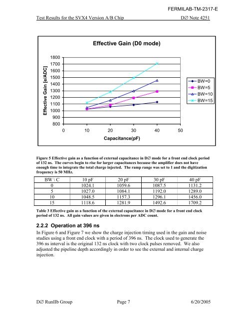
Effective Gain (D0 mode)<br />
Effective Gain [e/ADC]<br />
1800<br />
1700<br />
1600<br />
1500<br />
1400<br />
1300<br />
1200<br />
1100<br />
1000<br />
900<br />
800<br />
0 10 20 30 40 50<br />
Capacitance(pF)<br />
BW=0<br />
BW=5<br />
BW=10<br />
BW=15<br />
Figure 5 Effective gain as a function of external capacitance in D∅ mode for a front end clock period<br />
of 132 ns. The curves begin to rise for larger capacitances because the amplifier does not have<br />
enough time to integrate the total charge injected. The ramp range was set to 1 and the digitization<br />
frequency is 50 MHz.<br />
BW \ C 10 pF 20 pF 30 pF 40 pF<br />
0 1024.1 1059.6 1087.5 1131.2<br />
5 1027.0 1084.1 1192.0 1289.0<br />
10 1048.5 1157.3 1296.1 1456.0<br />
15 1118.6 1281.9 1492.6 1709.2<br />
Table 3 Effective gain as a function of the external capacitance in D∅ mode for a front end clock<br />
period of 132 ns. All gain values are given in electrons per ADC count.<br />
2.2.2 Operation at 396 ns<br />
In Figure 6 and Figure 7 we show the charge injection timing used in the gain and noise<br />
studies using a front end clock with a period of 396 ns. The clock used to generate the<br />
396 ns interval is the original 132 ns clock with two clock pulses removed. We also<br />
adjusted the pipeline depth accordingly in order to see the external and internal charge<br />
injection.<br />
D∅ RunIIb Group Page 7 6/20/2005