Graphene-on-SiC - ISOM
Graphene-on-SiC - ISOM
Graphene-on-SiC - ISOM

Create successful ePaper yourself
Turn your PDF publications into a flip-book with our unique Google optimized e-Paper software.
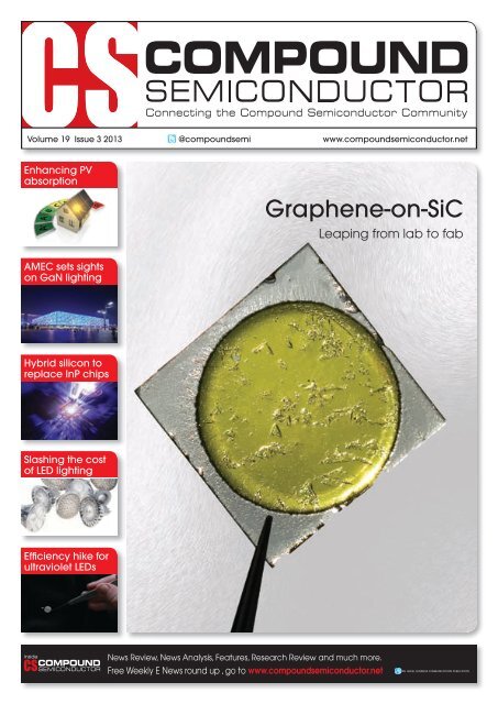
Volume 19 Issue 3 2013 @compoundsemi www.compoundsemic<strong>on</strong>ductor.net<br />
Enhancing PV<br />
absorpti<strong>on</strong><br />
<str<strong>on</strong>g>Graphene</str<strong>on</strong>g>-<strong>on</strong>-<strong>SiC</strong><br />
Leaping from lab to fab<br />
AMEC sets sights<br />
<strong>on</strong> GaN lighting<br />
Hybrid silic<strong>on</strong> to<br />
replace InP chips<br />
Slashing the cost<br />
of LED lighting<br />
Effi ciency hike for<br />
ultraviolet LEDs<br />
News Review, News Analysis, Features, Research Review and much more.<br />
Free Weekly E News round up , go to www.compoundsemic<strong>on</strong>ductor.net
200mm GaN-<strong>on</strong>-Si Batch Reactor<br />
5x200mm<br />
AIX G5+<br />
AIX G5+ for GaN-<strong>on</strong>-Si<br />
■ Dedicated technology package<br />
■ Compatible with the AIX G5 HT platform<br />
■ Enables Si-style mass manufacturing<br />
■ Builds <strong>on</strong> planetary technology:<br />
Excellent and symmetric uniformities,<br />
c<strong>on</strong>trolled bow behavior,<br />
using standard Si substrates.<br />
AIXTRON SE · info@aixtr<strong>on</strong>.com · www.aixtr<strong>on</strong>.com
editorialview<br />
by Dr Richard Stevens<strong>on</strong>, Editor<br />
The wide bandgap war<br />
Wide bandgap poWer electr<strong>on</strong>ics is the hottest<br />
sector within our industry. sales in this market are tipped to<br />
rocket throughout the foreseeable future, leading to annual<br />
revenues for sic and gan devices to hit around $1 billi<strong>on</strong> or<br />
more by 2020.<br />
at the hugely successful cs internati<strong>on</strong>al,<br />
which was held this March, a high proporti<strong>on</strong> of<br />
presentati<strong>on</strong>s detailed advances in both classes<br />
of transistor and diode, and leading analysts<br />
predicted where these devices could make an<br />
impact.<br />
in the l<strong>on</strong>g-term, they’ll see deployment in the<br />
grid. but they’ll need a stepping-st<strong>on</strong>e to get<br />
there, which could well be the solar inverter:<br />
the time taken to recoup the additi<strong>on</strong>al outlay<br />
over an all-silic<strong>on</strong> system is dropping from a few<br />
years to a matter of m<strong>on</strong>ths, and this will spur<br />
sales of wide bandgap products in this sector.<br />
Which widegap material has the greater success in a particular<br />
applicati<strong>on</strong> may be decided by the maximum operating<br />
voltage of the device. at voltages below 1 kV, many believe<br />
that gan-<strong>on</strong>-silic<strong>on</strong> devices will be more successful than their<br />
sic cousins, due to a combinati<strong>on</strong> of lower cost and superior<br />
performance to silic<strong>on</strong> equivalents. but bey<strong>on</strong>d 1 kV, sic is<br />
tipped to dominate, because it is felt that gan-<strong>on</strong>-silic<strong>on</strong> cannot<br />
handle such high voltages.<br />
not every<strong>on</strong>e agrees with this view. a partnership from M/a<br />
com, Mit and the Us department of energy has shown that<br />
it is possible to c<strong>on</strong>struct gan-<strong>on</strong>-silic<strong>on</strong> diodes and HeMts<br />
with breakdown voltages well in excess of 2 kV.<br />
the way to do this, which is detailed in the feature “boosting<br />
gan-<strong>on</strong>-silic<strong>on</strong> blocking voltages” (see p42 ), is to use<br />
a combinati<strong>on</strong> of sophisticated buffer layers and<br />
a field plate. note that it is crucial to optimise the<br />
dimensi<strong>on</strong>s and locati<strong>on</strong> of this plate to enhance<br />
gan-<strong>on</strong>-silic<strong>on</strong> performance.<br />
this project has used commercially produced,<br />
100 mm, gan-<strong>on</strong>-silic<strong>on</strong> epiwafers, highlighting<br />
that this combinati<strong>on</strong> can combine low costs<br />
with high levels of performance.<br />
it will be interesting to see how quickly it takes for high-voltage<br />
devices made in this way to appear <strong>on</strong> the market, where they<br />
can compete with silic<strong>on</strong> incumbents and a handful of sic<br />
products. i, for <strong>on</strong>e, will find it intriguing to watch how the battle<br />
for the power electr<strong>on</strong>ics market pans out over the next decade.<br />
Editor dr richard stevens<strong>on</strong><br />
C<strong>on</strong>tributing Editor rebecca poole<br />
News Editor dr su Westwater<br />
Director of SEMI Publishing Jackie cann<strong>on</strong><br />
Senior Sales Executive robin Halder<br />
Sales Manager shehzad Munshi<br />
USA Rep: brun Media: tom brun<br />
Janice Jenkins<br />
Director of Logistics shar<strong>on</strong> cowley<br />
Design & Producti<strong>on</strong> Manager Mitchell gaynor<br />
Circulati<strong>on</strong> Director Jan smoothy<br />
richardstevens<strong>on</strong>@angelbc.com<br />
+44 (0)1291 629640<br />
editorial@rebeccapoole.com<br />
suwestwater@angelbc.com<br />
jackie.cann<strong>on</strong>@angelbc.com<br />
+44 (0)1923 690205<br />
robin.halder@angelbc.com<br />
+44 (0)2476 718109<br />
shehzad.munshi@angelbc.com<br />
+44 (0)1923 690215<br />
e: tbrun@brunmedia.com<br />
tel: +001 724 539-2404<br />
e: jjenkins@brunmedia.com<br />
tel: +001 724-929-3550<br />
shar<strong>on</strong>.cowley@angelbc.com<br />
+44 (0)1923 690200<br />
mitch.gaynor@angelbc.com<br />
+44 (0)1923 690214<br />
jan.smoothy@angelbc.com<br />
+44 (0)1923 690200<br />
Subscripti<strong>on</strong>s Manager debbie Higham<br />
debbie.higham@angelbc.com<br />
+44 (0)1923 690220<br />
Chief Operating Officer stephen Whitehurst<br />
stephen.whitehurst@angelbc.com<br />
+44 (0)2476 718970<br />
Directors bill dunlop Uprichard – ceo, stephen Whitehurst – coo, Jan smoothy – cFo,<br />
Jackie cann<strong>on</strong>, scott adams, shar<strong>on</strong> cowley, sukhi bhadal<br />
Published by angel business communicati<strong>on</strong>s ltd,<br />
Hannay House, 39 clarend<strong>on</strong> road, Watford, Herts Wd17 1Ja, UK.<br />
t: +44 (0)1923 690200<br />
F: +44 (0)1923 690201<br />
e: ask@angelbc.com<br />
angel business communicati<strong>on</strong>s ltd<br />
Unit 6, bow court, Fletchworth gate, burnsall road, coventry cV5 6sp, UK.<br />
t: +44 (0)2476 718 970 F: +44 (0)2476 718 971 e: info@angelbc.com<br />
compound semic<strong>on</strong>ductor is published eight times a year <strong>on</strong> a c<strong>on</strong>trolled circulati<strong>on</strong> basis. n<strong>on</strong>-qualifying individuals can subscribe at: £105.00/e158 pa (UK & europe), £138.00 pa (air mail), $198 pa (Usa).<br />
cover price £4.50. all informati<strong>on</strong> herein is believed to be correct at time of going to press. the publisher does not accept resp<strong>on</strong>sibility for any errors and omissi<strong>on</strong>s. the views expressed in this publicati<strong>on</strong><br />
are not necessarily those of the publisher. every effort has been made to obtain copyright permissi<strong>on</strong> for the material c<strong>on</strong>tained in this publicati<strong>on</strong>. angel business communicati<strong>on</strong>s ltd will be happy to<br />
acknowledge any copyright oversights in a subsequent issue of the publicati<strong>on</strong>. angel business communicati<strong>on</strong>s ltd © copyright 2013. all rights reserved. c<strong>on</strong>tents may not be reproduced in whole or<br />
part without the written c<strong>on</strong>sent of the publishers. the paper used within this magazine is produced by chain of custody certified manufacturers, guaranteeing sustainable sourcing.Us mailing informati<strong>on</strong>:<br />
compound semic<strong>on</strong>ductor, issn 1096-598X, is published 8 times a year, Jan/Feb, March, april/May, June, July, august/september, october, november/ december by angel business communicati<strong>on</strong>s ltd,<br />
Unit 6, bow court, Fletchworth gate, burnsall rd, coventry cV5 6sp. UK. the 2012 Us annual subscripti<strong>on</strong> price is $198. airfreight and mailing in the Usa by agent named air business ltd, c/o Worldnet<br />
shipping inc., 156-15, 146th avenue, 2nd Floor, Jamaica, nY 11434, Usa. periodicals postage paid at Jamaica nY 11431. Us postmaster: send address changes to compound semic<strong>on</strong>ductor,<br />
air business ltd, c/o Worldnet shipping inc., 156-15, 146th avenue, 2nd Floor, Jamaica, nY 11434, Usa. printed by: pensord press. issn 1096-598X (print) issn 2042-7328 (<strong>on</strong>line) © copyright 2013.<br />
April/May 2013 www.compoundsemic<strong>on</strong>ductor.net 3
10 9 8 7 6 5 4 3 2 1 0 1 2 3 4 5 6 7 8 9 10<br />
GaN epitaxy for<br />
power electr<strong>on</strong>ics<br />
• In-situ SiN capping layer<br />
- Optimal surface states passivati<strong>on</strong><br />
- Material robustness<br />
- Enhanced device reliability – stability<br />
• Wafer Diameter: up to 200 mm<br />
• Materials capability:<br />
- SiN/AlGaN/GaN HEMTs<br />
- SiN/AlN/GaN<br />
- (In)(Al)GaN – based heterostructures<br />
• Substrates:<br />
- Si (111)<br />
- <strong>SiC</strong><br />
For more informati<strong>on</strong>, please visit www.epigan.com<br />
or c<strong>on</strong>tact info@epigan.com<br />
EpiGaN nv · Kempische Steenweg 293 · B-3500 Hasselt · Belgium · Ph<strong>on</strong>e +32 11 56 66 20<br />
10 9 8 7 6 5 4 3 2 1 0 1 2 3 4 5 6 7 8 9 10
Volume 19 Issue 3 2013 @compoundsemi www.compoundsemic<strong>on</strong>ductor.net<br />
News Review, News Analysis, Features, Research Review and much more.<br />
Free Weekly E News round up , go to www.compoundsemic<strong>on</strong>ductor.net<br />
Leaping from lab to fab<br />
c<strong>on</strong>tents<br />
Volume 19 Issue 3 2013<br />
C<strong>on</strong>neCtIng the CoMPoUnD SeMIC<strong>on</strong>DUCtor CoMMUnIty<br />
features<br />
26<br />
30<br />
42<br />
46<br />
52<br />
59<br />
graphene-<strong>on</strong>-<strong>SiC</strong> heads from lab to fab<br />
To fulfil the tremendous potential of graphene, high-quality material must<br />
be shipped in significant volumes. One supplier looking to do just that is<br />
Graphensic, which has developed graphene-<strong>on</strong> <strong>SiC</strong> products for making<br />
structures for metrology, high-speed transistors and biosensors.<br />
Strategies for photovoltaic performance<br />
There are many opti<strong>on</strong>s for improving the performance of III-V solar cells,<br />
including inserting quantum wells and dots to extend spectral coverage<br />
and adding nanoparticles and diffracti<strong>on</strong> gratings to boost light trapping.<br />
Boosting gan-<strong>on</strong>-silic<strong>on</strong> blocking voltages<br />
A misc<strong>on</strong>cepti<strong>on</strong> is holding back the development and deployment of<br />
GaN devices that are built <strong>on</strong> silic<strong>on</strong> substrates. This platform is widely<br />
blamed for compromising blocking voltages, but it doesn’t: It is possible to<br />
make diodes and HEMTs <strong>on</strong> silic<strong>on</strong> that have breakdown voltages of well<br />
over 2 kV.<br />
Addressing the big issues at CS Internati<strong>on</strong>al<br />
The impact of Qualcomm’s CMOS amplifier <strong>on</strong> the GaAs RF market, the<br />
steps that must be taken to make LED light bulbs affordable, and the<br />
most likely path that will be taken to enable the introducti<strong>on</strong> of power<br />
electr<strong>on</strong>ics in the grid were all discussed by leading market analysts at<br />
CS Internati<strong>on</strong>al.<br />
gan Fets inch closer to volume producti<strong>on</strong><br />
Like many companies around the world, RF Micro Devices and<br />
Transphorm are moving from the development of GaN FETs to their<br />
producti<strong>on</strong>. How far have these firms progressed?<br />
research review<br />
Crystalline GaN grows <strong>on</strong> an amorphous platform<br />
Upping the efficiency of ultraviolet LEDs<br />
Eliminating the buffer between InGaN and silic<strong>on</strong><br />
26<br />
30<br />
Enhancing PV<br />
absorpti<strong>on</strong><br />
AMEC sets sights<br />
<strong>on</strong> GaN lighting<br />
Hybrid silic<strong>on</strong> to<br />
replace InP chips<br />
Slashing the cost<br />
of LED lighting<br />
Effi ciency hike for<br />
ultraviolet LEDs<br />
<str<strong>on</strong>g>Graphene</str<strong>on</strong>g>-<strong>on</strong>-<strong>SiC</strong><br />
NEWS: 06 Plessey releases first 6-inch GaN-<strong>on</strong>-silic<strong>on</strong><br />
LED products 07 Avago to acquire InP innovator<br />
CyOptics 08 First Solar’s CdTe sets total area efficiency<br />
record 10 Nitride semic<strong>on</strong>ductors set a new benchmark<br />
for UV LED output power 11 Sol Voltaics GaAs<br />
nanowires boost solar performance by 25 percent<br />
12 Aledia grows 3D GaN LEDs <strong>on</strong> 8 inch silic<strong>on</strong><br />
46<br />
NEWS ANALYSIS: 16 AMEC sets sights <strong>on</strong> GaN<br />
lighting 18 Hybrid silic<strong>on</strong> prepares to displace InP<br />
phot<strong>on</strong>ic chips 20 Lower cost LED lighting 22 The<br />
Qualcomm 4G radio chip: Hit or hype? 23 UV LEDs:<br />
Will substrates slow growth? 24 <strong>SiC</strong> infiltrates<br />
inverter markets<br />
Magazine & Fr<strong>on</strong>t Cover: Designed by Mitch Gaynor<br />
52<br />
April/May 2013 www.compoundsemic<strong>on</strong>ductor.net 5
NEWS REVIEW<br />
Plessey releases first 6-inch GaN-<strong>on</strong>-silic<strong>on</strong><br />
LED products<br />
pleSSey has announced that samples<br />
of its GaN <strong>on</strong> silic<strong>on</strong> leD products are<br />
now available. the company says these<br />
entry level products are the first leDs<br />
manufactured <strong>on</strong> 6-inch GaN-<strong>on</strong>-silic<strong>on</strong><br />
substrates to be commercially available<br />
anywhere in the world.<br />
plessey is using its proprietary large<br />
diameter GaN <strong>on</strong> silic<strong>on</strong> process<br />
technology to manufacture the leDs <strong>on</strong><br />
its 6-inch MaGIc (Manufactured <strong>on</strong> GaN<br />
I/c) line at its plymouth, england facility.<br />
the use of plessey’s MaGIc GaN<br />
line using standard semic<strong>on</strong>ductor<br />
manufacturing processing provides yield<br />
entitlements of greater than 95 percent<br />
and fast processing times providing a<br />
significant cost advantage over sapphire<br />
and Sic based soluti<strong>on</strong>s for leDs of<br />
similar quality.<br />
the release of the availability of plessey’s<br />
GaN <strong>on</strong> silic<strong>on</strong> leDs was coincident with<br />
a visit to the plessey plymouth facility by<br />
the rt. H<strong>on</strong>. Vince cable, Mp, Secretary<br />
of State for business Innovati<strong>on</strong> and<br />
Skills and president of the board of<br />
trade.<br />
applicati<strong>on</strong>s.” We will c<strong>on</strong>tinue to make<br />
progress in output efficiency and are<br />
<strong>on</strong> plan to release further improvements<br />
in light output throughout this year and<br />
into next. the operating and unit costs<br />
are <strong>on</strong> plan and we are seeing a number<br />
of routes to enhance our cost advantage<br />
over competing technologies,” c<strong>on</strong>tinues<br />
Denningt<strong>on</strong>.<br />
the MaGIc leD technology was<br />
transferred from cambridge University<br />
with the help of Dandan Zhu from the<br />
cambridge centre for Gallium Nitride,<br />
Sim<strong>on</strong> Westwater and antoine pujol from<br />
plessey Semic<strong>on</strong>ductors. at cambridge,<br />
the leDs are grown <strong>on</strong> a 6 x 2” thomas<br />
Swan (now aixtr<strong>on</strong>) reactor, whereas at<br />
plessey, they are grown <strong>on</strong> an aixtr<strong>on</strong><br />
crIUS II-Xl 7 x 6” platform.<br />
leDs and the associated solid state<br />
lighting soluti<strong>on</strong>s are due to become the<br />
dominant form of lighting in all forms in<br />
within the next five years.<br />
Solid state lighting is an energy efficient<br />
eco-friendly technology that will save<br />
billi<strong>on</strong>s of t<strong>on</strong>s of carb<strong>on</strong> emissi<strong>on</strong>s<br />
when fully implemented.<br />
there are also no recycling issues<br />
that fluorescent lighting poses with<br />
mercury c<strong>on</strong>tent.<br />
business Secretary Vince cable<br />
comments, “the government is<br />
supporting innovative companies like<br />
plessey who are growing, creating jobs<br />
and exporting their products all over the<br />
world. that’s why we selected plessey’s<br />
£3.25 milli<strong>on</strong> regi<strong>on</strong>al Growth Fund<br />
bid for Government support, which will<br />
create 100 new, high tech and highly<br />
skilled jobs in the regi<strong>on</strong>.”<br />
Michael leGoff, ceo plessey says, “We<br />
are very pleased to welcome Secretary of<br />
State Vince cable today. the department<br />
of business Innovati<strong>on</strong> and Skills has<br />
been very supportive of our efforts to<br />
date and with the launch of our first<br />
range of leDs today we are now looking<br />
towards aggressive growth in the solid<br />
state lighting markets.”<br />
“today is a significant step for us” adds<br />
barry Denningt<strong>on</strong>, plessey’s coo. “From<br />
acquiring our first MocVD reactor in<br />
august 2012 to having our first product<br />
in april 2013 is excellent progress.<br />
these entry level products will be<br />
used in indicating and accent lighting<br />
Spectrolab n<strong>on</strong>-c<strong>on</strong>centrator cell<br />
raises the bar<br />
Spectrolab has achieved a solar cell efficiency of 37.8 percent without<br />
c<strong>on</strong>centrati<strong>on</strong>. this is the comm<strong>on</strong> practice of having lenses or mirrors focus solar<br />
rays <strong>on</strong> the cells.<br />
this world record in ground-based solar cell efficiency was verified by the U.S.<br />
Department of energy’s Nati<strong>on</strong>al renewable energy laboratory in Golden,<br />
colorado. the cells use a new class of high-efficiency multi-juncti<strong>on</strong> solar<br />
cell, created from two or more compound semic<strong>on</strong>ductors, leveraging boeing<br />
technology that makes such materials more reliable.<br />
“We expect this solar cell technology will have significant benefits for space,<br />
ground-based, and sensor applicati<strong>on</strong>s,” says troy Daws<strong>on</strong>, president of Spectrolab.<br />
Spectrolab believes this solar cell technology can attain higher levels of efficiency,<br />
“possibly more than 45 percent even under low c<strong>on</strong>centrati<strong>on</strong>s,” according to<br />
Nasser Karam, the company’s Vp for advanced technology.<br />
Spectrolab, which is part of the boeing Defence, Space & Security unit, is a<br />
merchant supplier of high-efficiency multi-juncti<strong>on</strong> solar cells and panels for<br />
c<strong>on</strong>centrated photovoltaic and spacecraft power systems. Spectrolab offers sensors<br />
and solar simulators, in additi<strong>on</strong> to being a provider of airborne searchlights.<br />
6 www.compoundsemic<strong>on</strong>ductor.net April/May 2013
NEWS REVIEW<br />
Avago to acquire InP innovator CyOptics<br />
aNaloGUe INterFace comp<strong>on</strong>ent<br />
supplier avago technologies has<br />
signed a definitive agreement to acquire<br />
cyoptics.<br />
cyoptics specialises in Inp optical<br />
chip and comp<strong>on</strong>ent technologies<br />
for the data communicati<strong>on</strong>s and<br />
telecommunicati<strong>on</strong>s markets.<br />
the aggregate acquisiti<strong>on</strong> price will be<br />
approximately US$400 milli<strong>on</strong> in cash.<br />
avago’s optical transceiver products<br />
primarily utilise VcSel-based technology.<br />
avago believes the acquisiti<strong>on</strong> of<br />
cyoptics will strengthen its fibre optics<br />
product portfolio for emerging 40G<br />
and 100G enterprise and data centre<br />
applicati<strong>on</strong>s.<br />
cyoptics’ single-mode Inp laser, receiver<br />
and phot<strong>on</strong>ics integrati<strong>on</strong> capability will<br />
help extend avago’s technology in these<br />
applicati<strong>on</strong>s. the acquisiti<strong>on</strong> of cyoptics<br />
will facilitate avago’s establishment of<br />
a complementary optical comp<strong>on</strong>ents<br />
business, not <strong>on</strong>ly to serve growing<br />
segments of the access, metro and l<strong>on</strong>ghaul<br />
markets, but also for enterprise and<br />
data centre segments.<br />
cyoptics designs, fabricates and<br />
packages a broad portfolio of optical<br />
comp<strong>on</strong>ent products across enterprise,<br />
data centre, access, metro and l<strong>on</strong>g-haul<br />
market segments.<br />
cyoptics’ optical comp<strong>on</strong>ents are<br />
integrated into optical transceivers,<br />
transp<strong>on</strong>ders and line cards. leveraging<br />
its bell labs and lucent heritage,<br />
cyoptics has built a broad product<br />
portfolio and a customer base that<br />
includes the leading module and system<br />
oeMs. the firm’s revenues have more<br />
than tripled over the past three years.<br />
“We believe cyoptics’ leading Inp<br />
technology and optical manufacturing<br />
capability will strengthen avago’s fibre<br />
optics portfolio and accelerate our<br />
ability to capture next generati<strong>on</strong> 40G<br />
and 100G enterprise and data centre<br />
sockets,” says Hock tan, president and<br />
ceo of avago.<br />
“We are delighted to join avago<br />
technologies, a company with a l<strong>on</strong>g<br />
history of innovati<strong>on</strong> and a str<strong>on</strong>g<br />
positi<strong>on</strong> in the wired infrastructure<br />
market. We believe this transacti<strong>on</strong><br />
presents tremendous opportunities for<br />
our customers and our employees,”<br />
adds ed coringrato, president and<br />
ceo of cyoptics. “I would also like<br />
to take this opportunity to thank our l<strong>on</strong>g<br />
standing investors, JVp and especially<br />
their founder, Dr. erel Margalit, for their<br />
support and guidance over the past<br />
decade in building cyoptics into the<br />
significant industry participant it is today.<br />
My gratitude as well to our<br />
recent partners, ta associates, for their<br />
vote of c<strong>on</strong>fidence and support.”<br />
Philips and Optogan start LED producti<strong>on</strong> in Russia<br />
tHe GoVerNor of Saint-petersburg,<br />
Georgy poltavchenko, and anatoly<br />
chubais, ceo and chairman of the<br />
executive board of rusnano, has visited<br />
the producti<strong>on</strong> site of JSc optogan in<br />
St-petersburg, russia.<br />
this is where the joint venture (JV)<br />
“philips and optogan,” have launched<br />
the producti<strong>on</strong> line of the brand new leD<br />
luminaire “avenue”.<br />
the maximum capacity of the line is more<br />
than 50000 leD luminaries per year.<br />
the modern producti<strong>on</strong> line is capable<br />
of producing leD luminaries for street<br />
lighting according to the highest<br />
internati<strong>on</strong>al quality standards, energy<br />
efficiency and reliability.<br />
the visitors of the plant were dem<strong>on</strong>strated<br />
the brand new developments of “philips<br />
and optogan” for street and yard lighting,<br />
which allows the significant reducti<strong>on</strong><br />
of energy c<strong>on</strong>sumpti<strong>on</strong> without loss in<br />
light quality.<br />
the new leD luminaire “avenue” fits the<br />
whole range of ec<strong>on</strong>omic and technical<br />
requirements of the Saint-petersburg<br />
energy efficiency program. this launch<br />
allows “philips and optogan” to offer the<br />
“avenue” at the most competitive price<br />
ever - 8000 rubles.also the company<br />
experience of interacting with design<br />
bureaus str<strong>on</strong>gly supports the usage<br />
of JV leD luminaries. they are claimed<br />
to perform “perfectly” even <strong>on</strong> a1 class<br />
highways, with the placement of the 20<br />
metre lighting poles being 65 metres<br />
apart.<br />
“We appreciate the interest and support<br />
of the Governor of St. petersburg in<br />
the development of energy efficient<br />
technology in the regi<strong>on</strong>. We are satisfied<br />
that we have been able to present<br />
localised product families within such a<br />
short time which are fitting very well to<br />
russian market requirements,” andre<br />
richter, Head of “philips and optogan”<br />
comments. During the visit it was added<br />
that, “Indeed, this new leD luminaire will<br />
find a proper place in streets and yards<br />
lighting.”<br />
royal philips electr<strong>on</strong>ics and russian<br />
manufacturer of leD products optogan,<br />
announced the signing of the joint<br />
venture agreement in april 2012.<br />
the JV aims to become a str<strong>on</strong>g player in<br />
the fast growing leD road lighting market<br />
in russia.<br />
It took less than a year to launch the new<br />
producti<strong>on</strong> line at optogan’s producti<strong>on</strong><br />
site in St-petersburg.<br />
During the year, “philips and optogan”<br />
significantly improved its product<br />
portfolio both ec<strong>on</strong>omically and<br />
technically. thus, the price for leD<br />
luminaries in 2013 decreased by 30<br />
percent compared to the same kind of<br />
luminaries of 2012. this was coupled by<br />
a relative increase of energy efficiency of<br />
the luminaries of more than 10 percent.<br />
the russian leD road lighting market is<br />
expected to double to eUr 100 milli<strong>on</strong> by<br />
2015. the strategic initiatives of “philips<br />
and optogan” are totally in line with the<br />
company’s plans to take a leadership<br />
positi<strong>on</strong> in the market.<br />
April/May 2013 www.compoundsemic<strong>on</strong>ductor.net 7
NEWS REVIEW<br />
First Solar’s CdTe sets total<br />
area efficiency record<br />
FIrSt Solar has set a new world<br />
record for cdte photovoltaic (pV) module<br />
c<strong>on</strong>versi<strong>on</strong> efficiency. the firm has<br />
achieved a record 16.1 percent total area<br />
module efficiency in tests c<strong>on</strong>firmed by<br />
the U.S. Department of energy’s Nati<strong>on</strong>al<br />
renewable energy laboratory (Nrel).<br />
the new record is a substantial increase<br />
over the prior record of 14.4 percent<br />
efficiency, which the company set in<br />
January 2012.<br />
Separately, First Solar also set a record<br />
for cdte open circuit voltage (Voc), a<br />
critical parameter for pV performance,<br />
reaching 903.2mV in Nrel-certified<br />
testing. this new record marks the first<br />
substantial increase in cdte Voc in over<br />
a decade of internati<strong>on</strong>al r&D.<br />
the new records come just six weeks<br />
after First Solar announced a new world<br />
record for cdte solar cell efficiency of<br />
18.7 percent.<br />
transferring its success in the r&D lab to<br />
its commercial modules, First Solar also<br />
launched a new evoluti<strong>on</strong> of its Series 3<br />
thin-film pV module platform, the Series<br />
3 black. they incorporate First Solar’s<br />
latest advances in c<strong>on</strong>versi<strong>on</strong> efficiency<br />
as well as additi<strong>on</strong>al features to enhance<br />
its performance in utility-scale power<br />
plants.<br />
the all-black module’s change in<br />
appearance results from the use<br />
of an advanced, all-black edge<br />
seal technology combined with an<br />
innovative encapsulati<strong>on</strong> material that<br />
further enhances its field durability<br />
and dem<strong>on</strong>strates improvements in<br />
accelerated life testing results.<br />
the Series 3 black module maintains<br />
all the existing Iec certificati<strong>on</strong>s and<br />
Ul listings for the Series 3 family which<br />
enable the 1000V system designs that<br />
typify the company’s utility-scale power<br />
plants. First Solar began to implement<br />
the Series 3 black enhancements in<br />
producti<strong>on</strong> modules earlier this year.<br />
based <strong>on</strong> the company’s recordsetting<br />
technology and robust Series<br />
3 black platform, the company also<br />
has accelerated its module c<strong>on</strong>versi<strong>on</strong><br />
efficiency roadmap, raising its lead<br />
producti<strong>on</strong> line module efficiency target<br />
for 2015 to 15-16.2 percent.<br />
First Solar also extended its module<br />
c<strong>on</strong>versi<strong>on</strong> efficiency roadmap to 2017,<br />
with targets for lead producti<strong>on</strong> line<br />
module efficiency of 16.2 to 16.9 percent<br />
in 2016 and 16.4 to 17.1 percent in 2017.<br />
“We are especially proud of this new<br />
efficiency record because the technology<br />
was created for producti<strong>on</strong>-scale<br />
implementati<strong>on</strong>, as evidenced by our<br />
accelerated efficiency roadmaps,” says<br />
raffi Garabedian, First Solar’s chief<br />
technology officer.<br />
Aledia’s nano-<br />
LED research<br />
powers forward<br />
with Veeco<br />
cea-leti, a research lab based in<br />
Grenoble, France, has selected<br />
Veeco’s turboDisc K465i MocVD<br />
system for its program with aledia, its<br />
nanowire-leD partner.<br />
aledia, a start-up company spun<br />
out of the cea-leti labs in 2011,<br />
is based at the cea site. It counts<br />
am<strong>on</strong>g its three founders two former<br />
cea researchers, Xavier Hug<strong>on</strong> and<br />
philippe Gilet.<br />
aledia’s goal is to manufacture<br />
3D nanowire-based leDs for<br />
solid-state lighting applicati<strong>on</strong>s <strong>on</strong><br />
thin silic<strong>on</strong> wafer substrates, of 8<br />
inches or greater in diameter, at<br />
a cost significantly below that of<br />
c<strong>on</strong>venti<strong>on</strong>al planar leDs.<br />
Nanowires are thin crystalline<br />
structures that, when electrically<br />
charged, can emit a broader spectrum<br />
of light than c<strong>on</strong>venti<strong>on</strong>al leDs, and<br />
can be grown <strong>on</strong> industry-standard<br />
silic<strong>on</strong> substrates.<br />
aledia’s nanowire technology was<br />
originally developed at cea-leti,<br />
and aledia and cea-leti c<strong>on</strong>tinue to<br />
develop nanowire technology in close<br />
cooperati<strong>on</strong>.<br />
Fabrice Geiger, Head of cealeti’s<br />
Silic<strong>on</strong> technology Divisi<strong>on</strong>,<br />
comments, “We are c<strong>on</strong>fident that<br />
Veeco’s MocVD system is the<br />
right equipment to help make this<br />
technology successful.”<br />
the Series 3 black’s performance in a<br />
wide range of operating envir<strong>on</strong>ments is<br />
further validated by its new Iec 60068-<br />
2-68 “sand and dust test” certificati<strong>on</strong>,<br />
which measures durability in harsh<br />
desert envir<strong>on</strong>ments characterised by<br />
blowing abrasive sand.<br />
the certificati<strong>on</strong> complements existing<br />
Iec salt mist and amm<strong>on</strong>ia certificati<strong>on</strong>s<br />
to provide a comprehensive range of<br />
independent testing that reflects worldclass<br />
durability and performance in the<br />
harshest operating c<strong>on</strong>diti<strong>on</strong>s.<br />
“Measurements in the lab are an<br />
important benchmark, but our r&D<br />
missi<strong>on</strong> is to deliver technology that<br />
is designed to shine in real-world<br />
c<strong>on</strong>diti<strong>on</strong>s as part of our integrated<br />
power plant systems, engineered to<br />
deliver the best performance, reliability<br />
and value for our customers. the Series<br />
3 black is a testament to our integrated<br />
approach to product development,<br />
combining technological advances from<br />
the lab with years of real-world data and<br />
experience operating utility-scale power<br />
plants in harsh envir<strong>on</strong>ments.”<br />
according to Giorgio anania, aledia’s<br />
president and chief executive<br />
officer, “the turboDisc reactor<br />
will be an important element of<br />
our strategy to take this potentially<br />
game-changing technology towards<br />
the commercialisati<strong>on</strong> phase. In<br />
partnership with cea-leti, we<br />
selected Veeco because our analysis<br />
indicated that at this time their<br />
MocVD systems showed the best<br />
financial returns for 8 inch wafer<br />
producti<strong>on</strong> <strong>on</strong> the market.”<br />
8 www.compoundsemic<strong>on</strong>ductor.net April/May 2013
100 mm<br />
<strong>SiC</strong> WAFER<br />
150 mm<br />
<strong>SiC</strong> WAFER<br />
CREE <strong>SiC</strong> AND GaN MATERIALS<br />
MATERIALS<br />
PORTFOLIO<br />
Supported diameters:<br />
- 76.2 mm<br />
- 100.0 mm<br />
- 150.0 mm<br />
<strong>SiC</strong> substrates:<br />
- n-type<br />
- p-type<br />
- High Purity SI<br />
<strong>SiC</strong> epitaxy:<br />
- n-type<br />
- p-type<br />
- thick epitaxy<br />
INDUSTRY-LEADING PORTFOLIO,<br />
INNOVATION AND SCALE<br />
With more than 25 years of development and manufacturing experience, Cree is<br />
driving innovati<strong>on</strong> with the industry’s broadest range of <strong>SiC</strong> and GaN materials.<br />
Delivering substrate and epitaxy opti<strong>on</strong>s in up to 150 mm diameters, Cree provides a<br />
vertically integrated materials product offering combining industry-leading volume,<br />
scale, quality and vast intellectual property portfolio.<br />
When you partner with Cree you get the best materials and the brightest innovati<strong>on</strong>.<br />
Learn how Cree can revoluti<strong>on</strong>ize your designs at cree.com/materials<br />
or c<strong>on</strong>tact us at materials_sales@cree.com or +1 800 313 5300.<br />
GaN epitaxy:<br />
- GaN, AlN, AlGaN,<br />
InGaN, SiN layers<br />
- HEMT structures Cree materials are ISO/TS 16949 certified.
NEWS REVIEW<br />
Nitride semic<strong>on</strong>ductors set a new<br />
benchmark for UV LED output power<br />
NITRIDE SEMICONDUCTORS has<br />
released a portfolio of ultra-high power,<br />
ultra-violet LEDs delivering output<br />
powers that can be in excess of 3W.<br />
One of these LEDs, the NS380L-6SVR,<br />
produces 3200mW at 380 nm. According<br />
to Nitride Semic<strong>on</strong>ductors, the output<br />
of this LED at this wavelength exceeds<br />
all other commercial devices based <strong>on</strong><br />
a single chip. Nitride Semic<strong>on</strong>ductors<br />
has also launched a range of l<strong>on</strong>ger<br />
wavelength cousins, such as the<br />
NS400L-6SVR, which delivers an<br />
output of 3200mW at 400nm. The new<br />
range of chips combines an operating<br />
voltage of 4V with very high efficiencies.<br />
For example, driven at 800 mA, the<br />
NS380L-5SVR produces 700 mW at 380<br />
nm, equating to an external quantum<br />
efficiency of 35 percent. Meanwhile, the<br />
400 nm-emitting equivalent, the NS400L-<br />
5SVR, delivers an external quantum<br />
efficiency of 38.7 percent when driven at<br />
1000mA, and emitting 1200mW. Typically,<br />
ultraviolet LED chips have dimensi<strong>on</strong>s<br />
of around 1 mm by 1mm. For example,<br />
those made by SemiLEDs are 1.2 mm<br />
square, while those produced by Nichia<br />
are 1mm square. In c<strong>on</strong>trast, Nitride<br />
Semic<strong>on</strong>ductors’ ultraviolet LEDs are 2.2<br />
mm square - they are claimed to be the<br />
biggest <strong>on</strong> the market.<br />
Meister Abrasives<br />
Make A Quality Decisi<strong>on</strong><br />
Internati<strong>on</strong>al<br />
Advanced wafer thinning soluti<strong>on</strong>s<br />
for compound semic<strong>on</strong>ductors,<br />
power electr<strong>on</strong>ics, LEDs<br />
and semic<strong>on</strong>ductors<br />
– ask the Experts.<br />
Scaling the size of the chip while<br />
maintaining its performance is not trivial.<br />
Although increases in the chip’s size boost<br />
output, efficiency is often compromised,<br />
due to heating issues and inferior current<br />
spreading within the device.<br />
To address these issues, the engineers<br />
at Nitride Semic<strong>on</strong>ductors produce<br />
their UV LEDs in a different way. They<br />
have developed a new layer structure<br />
to release the heat efficiently and<br />
introduced an electrode designed to<br />
flow current uniformly. This has been<br />
accomplished by minimising crystal<br />
defects through optimisati<strong>on</strong> of epitaxial<br />
growth, and developing a vertical chip<br />
design with an optimal electrode pattern.<br />
The large size of these devices enables<br />
the company to produce a single-chip<br />
ultraviolet LED with an output of several<br />
Watts; competing designs tend to be<br />
based <strong>on</strong> multiple chips. According to<br />
the company, the benefits of a single chip<br />
design include simplificati<strong>on</strong> of optics<br />
and a low driving voltage - when multiple<br />
chips are used, they are c<strong>on</strong>nected in<br />
series.<br />
Meister Abrasives AG, Switzerland · www.meister-abrasives.com<br />
Ultra-violet LEDs are packaged in a<br />
surface mounted device format, and<br />
available in three sizes, ranging from 4.2<br />
mm square to 5.6 mm square. They are<br />
designed for good heat transmissi<strong>on</strong>,<br />
and because the thickness of package<br />
is <strong>on</strong>ly 1.3mm, they can be mounted<br />
in high density by reflow soldering.<br />
The range of LEDs, which have been<br />
produced at a manufacturing cost that<br />
is just <strong>on</strong>e tenth of that of the previous<br />
generati<strong>on</strong> of devices, will be available<br />
for sampling from April 2013. Reliability is<br />
quoted at 10,000 hours, and guaranteed<br />
for 1000 hours.<br />
10 www.compoundsemic<strong>on</strong>ductor.net April/May 2013
NEWS REVIEW<br />
Sol Voltaics GaAs nanowires<br />
boost solar performance<br />
by 25 percent<br />
sOL VOLtAIcs has unveiled solInk,<br />
an ec<strong>on</strong>omical nanomaterial that the<br />
company promises can increase the<br />
efficiency of thin film solar modules<br />
crystalline silic<strong>on</strong> or by up to 25 percent<br />
or more.<br />
this will lead to solar power plants and<br />
rooftop solar arrays that will generate<br />
far more electricity than today’s best<br />
commercially available systems.<br />
the increase in efficiency will allow<br />
solInk enhanced panels to deliver<br />
power at prices that competes directly<br />
against electricity from fossil fuel plants<br />
while improving the ec<strong>on</strong>omics for<br />
manufacturers.<br />
Global demand for solar energy is<br />
expected to grow from 29.8 gigawatts<br />
of new solar installati<strong>on</strong>s in 2012 to<br />
50.8 gigawatts in 2016, according to<br />
Greentech Media.<br />
“the best way to lower the cost of solar<br />
power is to raise the efficiency of solar<br />
modules,” explains David epstein, ceO<br />
of sol Voltaics. Approximately two-thirds<br />
of the cost of commercial solar systems<br />
revolves around land, labour costs<br />
and other factors that solar developers<br />
can’t directly c<strong>on</strong>trol. By raising the<br />
efficiency of solar modules, we give solar<br />
manufacturers the opportunity to sell<br />
more valuable, higher margin products<br />
and solar developers the opportunity<br />
to generate more power at a lower<br />
price with essentially the same physical<br />
assets.”<br />
to date, sol Voltaics has raised $11<br />
milli<strong>on</strong> from private investors including<br />
Industrif<strong>on</strong>den, foundati<strong>on</strong> Asset<br />
Management of sweden, teknoinvest,<br />
Provider, nano future Invest and scatec<br />
energy of norway.<br />
the company has received additi<strong>on</strong>al<br />
public funding from the european Uni<strong>on</strong>,<br />
Vinnova, nordic Innovati<strong>on</strong> centre, and<br />
others. sol Voltaics will raise $10 to $20<br />
milli<strong>on</strong> this year.<br />
sol Voltaic’s strategy revolves around<br />
two fundamental technologies: GaAs<br />
nanowires, thin strands of material that<br />
c<strong>on</strong>stitute the active ingredient in solInk,<br />
and Aerotaxy, an innovative process<br />
for producing nanowires created by<br />
company founder and Lund University<br />
professor Lars samuels<strong>on</strong>.<br />
GaAs has been used in solar technology<br />
for years because of its reliability and<br />
high c<strong>on</strong>versi<strong>on</strong> efficiencies. Orbiting<br />
satellites employ solar cells made from<br />
the material to power their internal<br />
systems. GaAs solar cells, however,<br />
typically cost far more to produce than<br />
crystalline silic<strong>on</strong> or thin film cells,<br />
thereby c<strong>on</strong>fining the material to niche<br />
market segments.<br />
solInk dramatically reduces the cost by<br />
minimising materials used; less than a<br />
gram of nanowires is added to crystalline<br />
silic<strong>on</strong> panels. With solInk , module<br />
manufacturers can make commercially<br />
feasible, high efficiency GaAs solar<br />
modules or multi-juncti<strong>on</strong> solar modules<br />
combining GaAs and crystalline silic<strong>on</strong>.<br />
solInk also enables light c<strong>on</strong>centrati<strong>on</strong><br />
without the use of optics or mechanical<br />
comp<strong>on</strong>ents. nanowires need <strong>on</strong>ly cover<br />
a small porti<strong>on</strong> of the surface area of a<br />
crystalline silic<strong>on</strong> or thin film solar cell to<br />
achieve substantially all of the benefits of<br />
adding GaAs.<br />
In a research paper published in science<br />
earlier this year, Lund University and<br />
sol Voltaics researchers dem<strong>on</strong>strated<br />
that indium phosphide (InP) nanowires<br />
covering just 12 percent of the substrate<br />
surface produced a solar cell with an<br />
efficiency of 13.8 percent. the results<br />
were certified by the fraunhofer Institute.<br />
the phenomen<strong>on</strong>, called Wave<br />
c<strong>on</strong>centrated Photovoltaics (WcPV),<br />
combined with the other advantages<br />
of GaAs nanowires leads to groundbreaking<br />
performance for solInk.<br />
Toshiba unveils<br />
new diodes<br />
for it <strong>SiC</strong> power<br />
devices<br />
tOshIBA will manufacture schottky<br />
Barrier Diodes (sBDs) as the first of its<br />
new line-up of sic products.<br />
the sBD is suited for applicati<strong>on</strong>s<br />
that include power c<strong>on</strong>diti<strong>on</strong>ers<br />
for photovoltaic power generati<strong>on</strong><br />
systems. sBDs can also act as<br />
replacements for silic<strong>on</strong> diodes in<br />
switching power supplies, where they<br />
are approximately 50 percent more<br />
efficient.<br />
sic power devices offer more stable<br />
operati<strong>on</strong> than current silic<strong>on</strong> devices<br />
- even at high voltages and currents<br />
- as they significantly reduce heat<br />
dissipati<strong>on</strong> during operati<strong>on</strong>.<br />
they meet diverse industry<br />
needs for smaller, more effective<br />
communicati<strong>on</strong>s devices and suit<br />
industrial applicati<strong>on</strong>s ranging from<br />
servers to inverters and trains to<br />
automotive systems.<br />
Analysts estimate that the sic power<br />
device market will grow to about<br />
10 times the current scale by 2020.<br />
toshiba aims to secure 30 percent<br />
market share in 2020 by strengthening<br />
its product line-up, starting with the<br />
launch of the new sBD.<br />
Producti<strong>on</strong> is at toshiba’s himeji<br />
Operati<strong>on</strong>s-semic<strong>on</strong>ductor in hyogo<br />
Prefecture, Japan.<br />
April/May 2013 www.compoundsemic<strong>on</strong>ductor.net 11
NEWS REVIEW<br />
Aledia grows 3D GaN LEDs <strong>on</strong> 8 inch silic<strong>on</strong><br />
ceA-Leti spin off Aledia, has made its<br />
first Gan LeDs <strong>on</strong> 8 inch (200mm) silic<strong>on</strong><br />
wafers. the cost of Aledia’s LeD 3D<br />
chips based <strong>on</strong> microwires is expected<br />
to be four times less than traditi<strong>on</strong>al<br />
planar (2D) LeDs.<br />
Aledia has announced its firstround<br />
financing totalling €10 milli<strong>on</strong><br />
(approximately $13 milli<strong>on</strong>) with Us and<br />
european investors, which was closed<br />
in 2012. Aledia solves the important<br />
cost issue in the very large and growing<br />
LeD market. the c<strong>on</strong>tinued integrati<strong>on</strong><br />
of LeDs into new applicati<strong>on</strong>s, such<br />
as general lighting, depends <strong>on</strong> LeDs<br />
becoming available at substantially lower<br />
prices than today.<br />
the company claims its microwire<br />
technology enables the steep cost<br />
reducti<strong>on</strong> that is vital for the further<br />
transiti<strong>on</strong> to LeD. the Aledia LeD<br />
technology, made <strong>on</strong> large silic<strong>on</strong><br />
wafers and with very low materials<br />
cost, represents a cost-disruptive<br />
soluti<strong>on</strong> to this problem. Also, the new<br />
LeD technology is compatible with<br />
silic<strong>on</strong> cMOs technology and will be<br />
manufactured directly in existing highvolume<br />
silic<strong>on</strong> foundries.<br />
“since our financing last year, we have<br />
scaled up our microwire manufacturing<br />
process and transferred it to 8 inch<br />
(200mm) silic<strong>on</strong> wafers. We can now push<br />
forward to optimise the performance of<br />
these products and bring them to market,”<br />
points out Giorgio Anania, Aledia cofounder,<br />
President and ceO.<br />
Investors in Aledia’s first-round<br />
financing included sofinnova Partners,<br />
a european venture capital fund and<br />
an active investor in energy; new-York<br />
based Braemar energy Ventures, a Us<br />
energy technology investor with various<br />
investments in the LeD and illuminati<strong>on</strong><br />
area; Demeter Partners, a francebased<br />
cleantech investor; and ceA<br />
Investissement, the venture capital arm of<br />
ceA, france’s commissariat à l’energie<br />
Atomique et aux energies Alternatives.<br />
“this is an innovative technology that<br />
can have a disruptive effect <strong>on</strong> the LeD<br />
market,” adds Ji<strong>on</strong>g Ma, partner at<br />
Braemar energy Ventures. “Braemar is<br />
committed to investing in companies<br />
like Aledia that have developed a<br />
breakthrough approach to LeD lighting<br />
to accommodate a rapidly changing<br />
market. We are excited about the future<br />
opportunities this investment will bring<br />
and the expansi<strong>on</strong> of Aledia’s market<br />
presence and product offerings.”<br />
“We are proud to participate in the new<br />
venture of Giorgio Anania, a successful<br />
entrepreneur already well known to<br />
sofinnova, and of an outstanding<br />
technical team, that could revoluti<strong>on</strong>ise<br />
the large and growing LeD market, both<br />
in cost and performance,” c<strong>on</strong>tinues<br />
Alessio Beverina of sofinnova Partners.<br />
“We believe that the development of<br />
LeD lighting is an important element<br />
of energy-efficiency in our ec<strong>on</strong>omies<br />
- lighting representing approximately<br />
20 percent of all electricity usage. A<br />
technology able to make a significant<br />
breakthrough in the cost-effectiveness of<br />
using LeDs and thereby accelerate their<br />
adopti<strong>on</strong> will have a major envir<strong>on</strong>mental<br />
and financial impact,” c<strong>on</strong>cludes sophie<br />
Paturle, partner at cleantech specialist<br />
Demeter Partners.<br />
12 www.compoundsemic<strong>on</strong>ductor.net April/May 2013
www.lesker.com<br />
to Navigate Obstacles<br />
KJLC ® has been an industry leader in the design, manufacturing and distributi<strong>on</strong> of vacuum technology<br />
products and services since 1954. Vacuum science is our business.<br />
All Things Vacuum.<br />
Divisi<strong>on</strong>s: Process Equipment | Materials | Manufacturing | Vacuum Mart TM<br />
13-020<br />
Advancing Electr<strong>on</strong>ics<br />
Materials Characterizati<strong>on</strong> Systems<br />
Explore transport properties of new materials that open up possibilities<br />
for future development in fields like: semic<strong>on</strong>ductors, organic electr<strong>on</strong>ics,<br />
solar energy, and spintr<strong>on</strong>ic materials.<br />
New materials have been the driving force<br />
behind every major breakthrough in the last<br />
century. Lake Shore provides the systems<br />
you need to pursue the next <strong>on</strong>e.<br />
Cryogenic probe stati<strong>on</strong>s<br />
Magnetometer systems<br />
Hall effect systems<br />
THz characterizati<strong>on</strong> systems<br />
614.891.2243 | www.lakeshore.com
CS CONFERENCE REVIEW<br />
The CS Internati<strong>on</strong>al<br />
team would like to thank<br />
our sp<strong>on</strong>sors, speakers<br />
and delegates at this<br />
year’s c<strong>on</strong>ference<br />
and we look forward<br />
to seeing you all<br />
in 2014.<br />
www.cs-internati<strong>on</strong>al.net<br />
14 www.compoundsemic<strong>on</strong>ductor.net April/May 2013
CS CONFERENCE REVIEW<br />
April/May 2013 www.compoundsemic<strong>on</strong>ductor.net 15
NEWS ANALYSIS<br />
this mARCh, semic<strong>on</strong>ductor equipment<br />
manufacturer, AmEC, launched its multireactor<br />
mOCVD cluster tool. At a time<br />
when equipment sales from Western<br />
mainstream suppliers, Veeco and<br />
Aixtr<strong>on</strong>, have stalled <strong>on</strong> the back of the<br />
sluggish LED market, such a move could<br />
spell business suicide. Zhiyou Du, senior<br />
vice president of AmEC, thinks not.<br />
“Even though we have a recessi<strong>on</strong><br />
right now and the LED market it low, we<br />
str<strong>on</strong>gly believe the market will pick up<br />
by next year,” he says. “As a newcomer,<br />
this is the best time to enter the market.<br />
the customer is under less pressure to<br />
produce and has time to evaluate the<br />
tool.”<br />
“[the downturn] gives us about a year<br />
to qualify the tool with the customer and<br />
have our tool ready for the upturn,” he<br />
adds. so ready or not, what exactly is<br />
AmEC is offering? set-up in 2004, based<br />
in shanghai and widely regarded as<br />
China’s most successful chip-making<br />
equipment supplier, the company’s<br />
main business line to date has been<br />
dielectric etch tools for semic<strong>on</strong>ductor<br />
manufacturers.<br />
Raising hundreds of milli<strong>on</strong>s of dollars in<br />
funds from the likes of Goldman sachs,<br />
Qualcomm and samsung Ventures,<br />
AmEC has released etch tool after etch<br />
tool, all of which have been steadily<br />
adopted by Asia-based chip makers.<br />
Now, the business has set its sights<br />
<strong>on</strong> the solid state lighting market and<br />
introduced “Prismo D-Blue”, a mOCVD<br />
tool for high-volume producti<strong>on</strong> of GaNbased<br />
layer structures.<br />
As Du explains, the tool is based <strong>on</strong><br />
a four-reactor cluster architecture<br />
reducing its footprint by at least 30<br />
percent relative to competitors’ singlereactor<br />
tools. the four reactors can be<br />
c<strong>on</strong>trolled independently, with each<br />
processing up to 54 2-inch wafers<br />
depending <strong>on</strong> the batch c<strong>on</strong>figurati<strong>on</strong>.<br />
2-inch wafer trials have dem<strong>on</strong>strated<br />
impressive thickness uniformities; 0.4<br />
percent wafer-to-wafer uniformity and<br />
1 percent within-wafer uniformity. And<br />
moving to larger wafer sizes could be<br />
relatively easy.<br />
“We have some uniformity issues right<br />
now, but in general the hardware of<br />
the system will be the same, it will just<br />
require a little bit of process tuning to get<br />
the uniformity right,” says Du.<br />
AMEC sets sights <strong>on</strong> GaN lighting<br />
As MOCVD tool makers hang <strong>on</strong> for the LED upturn,<br />
an unexpected entrant from China is hoping<br />
to muscle in <strong>on</strong> the market share. Compound<br />
Semic<strong>on</strong>ductor looks at AMEC’s master-plan.<br />
16 www.compoundsemic<strong>on</strong>ductor.net April/May 2013
NEWS ANALYSIS<br />
AmEC is sticking with GaN layers, and<br />
doesn’t intend to develop tools for<br />
arsenides and phosphides. And crucially<br />
for the relatively new China-based LED<br />
manufacturers, the team has focused<br />
<strong>on</strong> ease-of-use. While the chamber<br />
of a competitor’s tool has to be<br />
opened and the shower head cleaned<br />
after every batch run, AmEC’s tool<br />
doesn’t.<br />
“Operators just d<strong>on</strong>’t want to do this,”<br />
says Du. “the industry is getting more<br />
automated and demanding more<br />
c<strong>on</strong>sistency.” And as Du adds, the<br />
software has been designed using<br />
semic<strong>on</strong>ductor industry standards<br />
creating a ‘very user-friendly’ interface.<br />
“this is a very stable, repeatable and<br />
reliable tool that customers can use,”<br />
he says.<br />
From dielectric etch to MOCVD tools: AMEC hopes to compete with the likes of Veeco and<br />
Aixtr<strong>on</strong> with its Prismo D-Blue<br />
the company will first focus <strong>on</strong> the shortterm<br />
opportunities in China and then the<br />
rest of the Asian market, with Europe<br />
and the Us coming later. Du is certain<br />
LED makers will be ready to invest come<br />
2014, saying: “Already we have seen<br />
signs from first tier fabs in taiwan... we<br />
are more optimistic than we were at the<br />
beginning of the year.”<br />
so should Veeco and Aixtr<strong>on</strong> worry<br />
yet? Probably not. As ims Research<br />
analyst, Alice tao, points out, the big<br />
two currently hold more than 90 percent<br />
mOCVD market share and are the <strong>on</strong>ly<br />
tool suppliers recording multiple sales<br />
over c<strong>on</strong>secutive quarters. But looking to<br />
the future, she believes AmEC and other<br />
Chinese competitors may be able to<br />
seize several opportunities.<br />
As part of its “twelfth Five Year Plan”<br />
running from 2010 to 2015, the Chinese<br />
government identified the large-scale<br />
adopti<strong>on</strong> of mOCVD tools as a priority;<br />
subsidies to domestic suppliers may<br />
return.<br />
China has the largest demand for these<br />
tools; overcapacity still exists but as<br />
the market picks up, replacements<br />
from China-based tool makers may be<br />
favoured. And Chinese tools may be<br />
cheaper.<br />
tao cites some Chinese equipment<br />
suppliers as saying home-grown tools<br />
could be up to 40 percent cheaper but<br />
questi<strong>on</strong>s running costs. meanwhile,<br />
AmEC expects overall cost-of-ownership<br />
of its product to be around 20 percent<br />
lower than ‘industry-leading’ tools.<br />
still, the company has several milest<strong>on</strong>es<br />
to reach before it can begin to rival<br />
the industry heavy weights. Yield figures<br />
are not yet available; as Du says:<br />
“We’re not running at producti<strong>on</strong> levels<br />
yet... but will have numbers in a m<strong>on</strong>th<br />
or so.”<br />
And results from 4-inch wafer trials, and<br />
bey<strong>on</strong>d, have yet to surface. Again,<br />
Du says his team has achieved pretty<br />
good results, but is working <strong>on</strong> tuning<br />
the process. But as tao told Compound<br />
Semic<strong>on</strong>ductor: “i’ve talked to AmEC<br />
and they seem very c<strong>on</strong>fident. they are<br />
successful in the semic<strong>on</strong>ductor industry,<br />
so it’s possible that they might be able to<br />
compete with Aixtr<strong>on</strong> or Veeco in the near<br />
future.”<br />
indeed, the tool is currently available<br />
for beta evaluati<strong>on</strong> at customer’s LED<br />
producti<strong>on</strong> lines. As tao c<strong>on</strong>cludes: “We<br />
still need to hear from the real users<br />
about the performance of these new tools<br />
and this make take a l<strong>on</strong>ger time.”<br />
© 2013 Angel Business Communicati<strong>on</strong>s.<br />
Permissi<strong>on</strong> required.<br />
April/May 2013 www.compoundsemic<strong>on</strong>ductor.net 17
NEWS ANALYSIS<br />
Hybrid silic<strong>on</strong> prepares<br />
to displace InP<br />
phot<strong>on</strong>ic chips<br />
Will hybrid silic<strong>on</strong> be the platform of choice<br />
for complex phot<strong>on</strong>ic integrated circuits?<br />
Compound Semic<strong>on</strong>ductor talks to<br />
Martijn Heck from the University of<br />
California, Santa Barbara, to find out more.<br />
in 2006, rEsEarChErs at thE<br />
UniVErsitY oF CaliFornia, santa<br />
Barbara, and intel unveiled the world’s<br />
first electrically pumped hybrid silic<strong>on</strong><br />
laser. taking advantage of the lightemitting<br />
properties of iii-V semic<strong>on</strong>ductors<br />
as well as mature Cmos processes to<br />
fabricate lasers <strong>on</strong> a silic<strong>on</strong> wafer, the<br />
device unlocked the door to cheap, massproduced<br />
silic<strong>on</strong> optical devices.<br />
Fast forward seven years and many<br />
believe the stage is now well and truly set<br />
for a hybrid silic<strong>on</strong> phot<strong>on</strong>ic revoluti<strong>on</strong>.<br />
myriad hybrid devices − from laser<br />
sources and optical amplifiers to highspeed<br />
modulators, waveguides and<br />
polarisati<strong>on</strong> comp<strong>on</strong>ents − have been<br />
developed, forming the building blocks<br />
of phot<strong>on</strong>ic integrated circuits (PiCs).<br />
UCsB has developed tapered mode<br />
c<strong>on</strong>verters to integrate hybrid silic<strong>on</strong><br />
comp<strong>on</strong>ents with passive silic<strong>on</strong>-<strong>on</strong>insulator<br />
substrates and used quantum<br />
well intermixing and die-b<strong>on</strong>ding to<br />
18 www.compoundsemic<strong>on</strong>ductor.net April/May 2013
NEWS ANALYSIS<br />
and make these high-performance, high<br />
functi<strong>on</strong>ality phot<strong>on</strong>ic integrated circuits.”<br />
this breathtaking rate of progress cannot<br />
fail to impress, but inP PiCs still very<br />
much have the edge. infinera is currently<br />
shipping optical network platforms built<br />
using 500 Gbit/s PiCs, and recently<br />
dem<strong>on</strong>strated a 10 tbit/s PiC. But could<br />
this so<strong>on</strong> change?<br />
heck and colleagues recently plotted<br />
a chart, showing the development of<br />
inP and hybrid silic<strong>on</strong> chip complexity,<br />
measured as the number of comp<strong>on</strong>ents<br />
per chip. Without a doubt, inP-based<br />
m<strong>on</strong>olithic integrati<strong>on</strong> has increased<br />
in complexity exp<strong>on</strong>entially over the<br />
past two decades, but according to the<br />
researchers, hybrid silic<strong>on</strong> PiCs are<br />
catching up, and fast. heck believes<br />
three key drivers are resp<strong>on</strong>sible for the<br />
technology’s speedy transformati<strong>on</strong>.<br />
“First, we are building <strong>on</strong> mature iii-V<br />
technology; we’re taking existing<br />
knowledge and putting it <strong>on</strong> a silic<strong>on</strong><br />
substrate,” he says. “For example we can<br />
now fabricate 70 Ghz modulators, and<br />
faster... this shows what a lot of progress<br />
we have made with the comp<strong>on</strong>ents.”<br />
sec<strong>on</strong>dly, according to heck, hybridsilic<strong>on</strong><br />
PiCs also make use of the mature<br />
Cmos fabricati<strong>on</strong> infrastructure for<br />
at least part of the process flow. and<br />
thirdly, he adds: “industry adopti<strong>on</strong> has<br />
been very quick. intel, hP and more are<br />
working <strong>on</strong> this and there is a very str<strong>on</strong>g<br />
effort in Europe. People recognise the<br />
potential for this technology.”<br />
and while the gap between hybrid<br />
silic<strong>on</strong> and inP remains large − tens<br />
of comp<strong>on</strong>ents can be integrated<br />
<strong>on</strong> a silic<strong>on</strong> PiC while hundreds are<br />
squeezed <strong>on</strong>to the inP equivalent − the<br />
forthcoming data deluge could drive<br />
change. Future terabit-per-sec<strong>on</strong>d<br />
datacom and interc<strong>on</strong>nect applicati<strong>on</strong>s<br />
will demand large volumes of highly<br />
integrated PiCs. and hybrid silic<strong>on</strong> with<br />
its 300 mm silic<strong>on</strong> substrates and Cmoscompatible<br />
fabricati<strong>on</strong>, offers far better<br />
ec<strong>on</strong>omics of scale than the inP-based<br />
PiC. heck is c<strong>on</strong>fident future datacoms<br />
and telecoms applicati<strong>on</strong>s will drive<br />
integrati<strong>on</strong> of hybrid silic<strong>on</strong> phot<strong>on</strong>ics,<br />
and recalls a recent roundtable event, led<br />
by UCsB’s institute of Energy Efficiency,<br />
that looked at how data centres of<br />
tomorrow will cope with data demands.<br />
“all the hot-shots from the main<br />
companies [intel, Cisco, hewlett Packard<br />
and amD to name but a few] were there<br />
and number <strong>on</strong>e <strong>on</strong> every<strong>on</strong>e’s list was<br />
phot<strong>on</strong>ics integrati<strong>on</strong>,” he says. “in terms<br />
of integrati<strong>on</strong>, we all know this is going to<br />
scale up. the steps are being taken by<br />
intel and other companies... yes this is<br />
slightly speculative, but comm<strong>on</strong> sense<br />
tells us it will happen.”<br />
© 2013 angel Business Communicati<strong>on</strong>s.<br />
Permissi<strong>on</strong> required.<br />
combine different bandgap comp<strong>on</strong>ents,<br />
and devices with different iii-V epitaxial<br />
stacks.<br />
across the industry, significant hybrid<br />
integrated circuits include highly<br />
integrated transmitters, optical phase<br />
arrays and optical packet switches. and<br />
headline news covers intel’s 50 Gbit/s<br />
silic<strong>on</strong> link, luxtera’s ‘milli<strong>on</strong>th’ chip<br />
and imec fabricating comp<strong>on</strong>ents <strong>on</strong><br />
300 mm silic<strong>on</strong> wafers. With these and<br />
other key players, from iBm to UCsB<br />
spin-off, aurri<strong>on</strong>, hurrying to light up<br />
the silic<strong>on</strong> chip, martijn heck from the<br />
optoelectr<strong>on</strong>ics research groups at<br />
UCsB believes today’s breakthroughs<br />
are just the beginning.<br />
“the promise [of integrating these<br />
comp<strong>on</strong>ents] has always been there, but<br />
we have now increased the yield while<br />
specifically looking at performance and<br />
processing,” he says. “the cool thing is<br />
we can now tie together the comp<strong>on</strong>ents<br />
Development of chip complexity measured as the number of comp<strong>on</strong>ents per chip<br />
[credit: MK Smit, JJGM. van der Tol, and MT Hill, “Moore’s law in phot<strong>on</strong>ics,”<br />
Laser Phot<strong>on</strong>. 6 1, 2012 and MJR Heck et al; “Hybrid Silic<strong>on</strong> Phot<strong>on</strong>ic Integrated<br />
Circuit Technology” JSTQE]<br />
April/May 2013 www.compoundsemic<strong>on</strong>ductor.net 19
NEWS ANALYSIS<br />
Lower cost LED lighting<br />
Will Cree’s $10 LED light bulb end America’s<br />
century-l<strong>on</strong>g incandescent love affair asks<br />
Compound Semic<strong>on</strong>ductor.<br />
as inDUstrY antiCiPatEs an lED<br />
market upturn, Cree has just unveiled a<br />
new line of lower-priced, incandescent<br />
look-alike bulbs that could speed the<br />
recovery. Costing from $10, coming<br />
with a ten year guarantee and offering<br />
a similar light output to the much-loved<br />
incandescent − but rated to 25,000,<br />
not 1000 hours − the bulbs have been<br />
developed specifically to kick-start<br />
sluggish domestic lighting markets<br />
across the Us.<br />
as Cree’s vice president of corporate<br />
marketing, mike Wats<strong>on</strong>, told Compound<br />
Semic<strong>on</strong>ductor: “We didn’t think this<br />
segment was moving fast enough so<br />
we’re giving c<strong>on</strong>sumers a reas<strong>on</strong> to<br />
switch to lED lighting. they love the<br />
shape and the light that comes out of the<br />
incandescent so we’ve given them a bulb<br />
that they are used to, at a price point they<br />
will try.”<br />
and the feedback is good. Described in<br />
the MIT Technology Review as “the lED<br />
bulb Edis<strong>on</strong> would love” and reported<br />
by many to “look like and light like” an<br />
incandescent, this is a bulb that the<br />
likes of Philips lighting and GE will find<br />
difficult to ignore. the new line of lED<br />
bulbs includes three models; a warm<br />
white 60 W-equivalent 9.5 W bulb priced<br />
at $ 12.97, a daylight 60 W-equivalent,<br />
9 W bulb at $ 13.97, and a warm white<br />
40 W-equivalent, 6 W bulb at $ 9.97.<br />
Each has a colour rendering index of at<br />
least 80 with both warm white versi<strong>on</strong>s<br />
emitting a 2700K pleasant warm light and<br />
the daylight bulb a cooler-looking 5000K<br />
light.<br />
meanwhile, the Philips lighting 60<br />
W-equivalent incandescent copy cat,<br />
delivers a cooler 3000K at 10 W for<br />
$14.97, while the GE lighting equivalent<br />
rings in at around $ 45. all bulbs promise<br />
a lifetime of around 25,000 hours, a<br />
l<strong>on</strong>g-term guarantee, but <strong>on</strong>ly the Cree<br />
bulb hits that magic $10 figure. so how<br />
does the lED heavyweight do it? a 40 W<br />
bulb comprises ten of Cree’s phosphorc<strong>on</strong>verted<br />
high voltage Xlamp Xt-E lEDs<br />
with the 60 W versi<strong>on</strong> c<strong>on</strong>taining twenty<br />
of the same. Phosphor is applied directly<br />
in the lED package to produce white<br />
light. Pairs of lEDs are mounted around<br />
the lamp’s heatsink with Cree calling<br />
the entire vertical structure the Filament<br />
tower.<br />
“the lEDs are arranged in a parallel<br />
c<strong>on</strong>figurati<strong>on</strong> to get as close as possible<br />
to the line voltage of the power supply,”<br />
says Wats<strong>on</strong>. “We can reduce the<br />
comp<strong>on</strong>ent count <strong>on</strong> the driver, making<br />
it simpler and lighter, and we need less<br />
metal, helping us to replicate the look of<br />
an incandescent bulb.”<br />
indeed, Wats<strong>on</strong> is keen to emphasise<br />
the simplicity of its latest bulb. “We’ve<br />
designed this 100 percent, and sourced<br />
the necessary comp<strong>on</strong>ents,” he says.<br />
“take it apart and you’ll see how<br />
simple and elegant it really is. We<br />
needed something that could fit into<br />
this form factor and give you the look<br />
of incandescent light, at a low enough<br />
cost.”<br />
Wats<strong>on</strong> asserts ‘entire system’<br />
breakthroughs − from the lED and power<br />
supply to optics and design − have<br />
been crucial to cutting costs but also<br />
attributes the $10 figure to the company’s<br />
structure. “We’re vertically integrated and<br />
can adjust many variables at the same<br />
time and better than if we were using the<br />
traditi<strong>on</strong>al supply chain,” he says. Vertical<br />
integrati<strong>on</strong> or not, many industry sources<br />
believe Cree is <strong>on</strong>to something. Pars<br />
mukish, analyst at Yole Développement,<br />
believes the bulb will serve its purpose<br />
and trigger greater c<strong>on</strong>sumer adopti<strong>on</strong> in<br />
the Us domestic lighting market.<br />
“today’s main issue with lED lighting<br />
for residential applicati<strong>on</strong>s is the upfr<strong>on</strong>t<br />
cost,” he says. “the incandescent<br />
costs less than a dollar, the compact<br />
fluorescent lamp costs between $3 and<br />
$5 while the lED lamp, before this, was<br />
between $15 and $40, depending <strong>on</strong><br />
geography and rebates offered.“<br />
But of course the Cree bulb changes this.<br />
and as mukish adds: “ in the previous<br />
era of lEDs, it was all about increasing<br />
Cree’s ‘Filament<br />
Tower’ mimics<br />
the filament of<br />
an incandescent<br />
light bulb<br />
the lumen per watt. now it is all about<br />
increasing the lumen per dollar... we<br />
think [Cree has] a good strategy as the<br />
potential volume triggered by residential<br />
lighting will be a virtuous circle for the<br />
company to c<strong>on</strong>tinue decreasing costs.”<br />
indeed, questi<strong>on</strong> Wats<strong>on</strong> whether<br />
the bulb could match the efficiency<br />
and quality of past winners of the<br />
Us Department of Energy’s l Prize<br />
competiti<strong>on</strong> and he bluntly says: “the<br />
l prize is fun, and industry rewards are<br />
fun, but the prize that Cree wants is<br />
c<strong>on</strong>sumer adopti<strong>on</strong>.”<br />
“the bulb is designed to meet Energy<br />
star requirements but has also been<br />
designed to be affordable with or without<br />
that. it can pay for itself in about a year...<br />
so without any rebate or government<br />
regulati<strong>on</strong> we have made the maths<br />
work,” he adds. “anything else we do<br />
<strong>on</strong> that [the efficiency] side will now just<br />
make this even sweeter.”<br />
so while the bulb is currently available<br />
in home Depot stores across the Us,<br />
what about the rest of the world? it<br />
will have to wait. Wats<strong>on</strong> believes the<br />
greatest demand currently lies in the Us,<br />
adding:“Europe uses a lot of recessed<br />
track lighting whereas the Us market<br />
already has a very large installed base of<br />
a lamps.”<br />
still Cree’s Us focus looks to be working;<br />
the release of the products saw Cree’s<br />
shares rise 13 percent to the highest level<br />
in two years. We have yet to see if Us<br />
c<strong>on</strong>sumers will snap up a $10 lED lamp,<br />
but at the very least, Cree has brought<br />
affordable lED lighting closer to home.<br />
© 2013 angel Business Communicati<strong>on</strong>s.<br />
Permissi<strong>on</strong> required.<br />
20 www.compoundsemic<strong>on</strong>ductor.net April/May 2013
Reprints are a valuable sales tool<br />
Benefit from a reprint featuring your company<br />
They can be ordered after publicati<strong>on</strong> and<br />
can be customised to your exact needs<br />
For more informati<strong>on</strong> and prices<br />
please c<strong>on</strong>tact the sales team.<br />
Robin Halder<br />
T: +44 (0)2476 718970<br />
E: robin.halder@angelbc.com<br />
Shehzad Munshi<br />
T: +44 (0)1923 690215<br />
E: shehzad.munshi@angelbc.com
NEWS ANALYSIS<br />
available wireless data standard but<br />
fragmentati<strong>on</strong> between the world’s lTesupported<br />
40 frequencies means it’s not<br />
universal across the uS and europe.<br />
But despite the hope, many analysts<br />
still questi<strong>on</strong> when this will take place.<br />
The new RF fr<strong>on</strong>t-end is slated to reach<br />
handsets later this year, and while<br />
the chipset could make 4G ph<strong>on</strong>es<br />
compatible throughout the uS and<br />
europe, compatibility across networks<br />
would be a problem, as operators haven’t<br />
yet c<strong>on</strong>firmed 4G roaming agreements.<br />
operator issues aside, the kneejerk<br />
reacti<strong>on</strong> of many has been that<br />
Qualcomm will not initially target<br />
the high-end markets dominated by<br />
compound semic<strong>on</strong>ductor power<br />
amplifier heavyweights. Research<br />
analyst Joanne Feeney from uS-based<br />
The Qualcomm 4G radio<br />
chip: Hit or hype?<br />
Qualcomm’s new radio chipset may take us<br />
closer to a global 4G ph<strong>on</strong>e, but does it really<br />
signal an end to GaAs power amps in handsets?<br />
market is moving into the mainstream,<br />
and you’re going to need a combinati<strong>on</strong><br />
of performance and cost.”<br />
anwar, like many, is also adamant Gaas<br />
still has the performance edge despite<br />
rapid progress from cmoS competitors.<br />
Qualcomm has worked hard <strong>on</strong> its<br />
envelope-tracking (eT) technology to<br />
reduce power c<strong>on</strong>sumpti<strong>on</strong> by up to 30<br />
percent, and nudge the efficiency of its<br />
power amplifiers closer to that of Gaas.<br />
at the same time, nujira has revealed<br />
“breakthrough” test results from a<br />
prototype cmoS power amplifier<br />
coupled with its envelope-tracking power<br />
modulators. chief executive, Tim haynes<br />
asserts: “The combinati<strong>on</strong> of cmoS Pas<br />
and nujira patented eT architectures<br />
could ultimately signal the death of the<br />
Gaas industry for handset applicati<strong>on</strong>s.”<br />
however, RFmD has now released new<br />
eT power management products, with<br />
president eric crevist<strong>on</strong> claiming to be<br />
“enthusiastic about the deployment of<br />
eT-based soluti<strong>on</strong>s”. as anwar highlights:<br />
“envelope tracking isn’t solely c<strong>on</strong>fined<br />
to cmoS Pas. RFmD has just announced<br />
eT for its Pas as well as Gaas Pas<br />
designed to work with Qualcomm’s eT.<br />
other Pa suppliers will follow with Pas<br />
designed for eT.”<br />
When Qualcomm unveiled its<br />
cmoS-based fr<strong>on</strong>t end module,<br />
shares of compound semic<strong>on</strong>ductor<br />
wireless chip vendors slumped.RFmD’s<br />
nose-dived by more than 14 percent,<br />
Skyworks’ dropped 13 percent, and<br />
TriQuint’s dipped by around 7 percent.<br />
Some analysts cut RF vendor ratings,<br />
describing Qualcomm’s release as a<br />
‘bombshell’, while further down the<br />
supply chain the shares of uK-based<br />
III-V wafer maker, IQe, fell more than 13<br />
percent in a day.<br />
now normality is returning, with shares<br />
of some industry players edging up.<br />
SkyWorks is busy showcasing its<br />
fr<strong>on</strong>t-end platform − boasting take-up<br />
from myriad oems − while RFmD has<br />
unveiled new power amplifiers and<br />
transmit modules. So was Qualcomm’s<br />
latest offering such a bombshell after all?<br />
Described as the first, single global<br />
4G lTe design for mobile devices,<br />
Qualcomm hopes its “RF360” will end<br />
roaming problems that see travellers allto-quickly<br />
bumped down to a 3G network.<br />
4G lTe is the fastest commercially<br />
l<strong>on</strong>gbow Research has stated that<br />
potential technology shortcomings −<br />
relative to Gaas power amplifiers − will<br />
see the chipset adopted in lower-end<br />
smartph<strong>on</strong>es.<br />
likewise, Raym<strong>on</strong>d James analyst,<br />
Tavis mccourt, highlighted uncertain<br />
performance, predicting the soluti<strong>on</strong><br />
would first penetrate chinese markets.<br />
Indeed, in a recent stockholder<br />
c<strong>on</strong>ference, Qualcomm chief executive<br />
Paul Jacobs said: “If we are focusing <strong>on</strong><br />
china, it’s been a great market for us...<br />
It’s the number <strong>on</strong>e smartph<strong>on</strong>e country<br />
in the world, 200 milli<strong>on</strong> smartph<strong>on</strong>es<br />
were shipped in china in 2012 with a<br />
growth of 132 percent year-over-year.”<br />
asif anwar, analyst at Strategic<br />
Technologies, uS, has a different take.<br />
“my initial reacti<strong>on</strong> was, yes, Qualcomm<br />
is going into the high-volume, low-end<br />
chinese market with this,” he says.<br />
“But then the company also talks<br />
about proprietary packaging giving a<br />
50 percent reducti<strong>on</strong> in board, this will<br />
be more expensive...The smartph<strong>on</strong>e<br />
Qualcomm also highlights how its latest<br />
fr<strong>on</strong>t-end, when combined with its Gobi<br />
or Snapdrag<strong>on</strong> baseband chip-sets, can<br />
provide a comprehensive soluti<strong>on</strong> that<br />
will help oems minimise development<br />
and design costs. as Jacobs highlighted<br />
in a recent stockholder c<strong>on</strong>ference,<br />
nokia lumia, Galaxy S3, hTc <strong>on</strong>e and<br />
S<strong>on</strong>y XperiaZ are all built <strong>on</strong> Snapdrag<strong>on</strong><br />
chipsets. But do high-end market players<br />
want a complete base-band and fr<strong>on</strong>tend<br />
soluti<strong>on</strong>?<br />
“If you open up an apple or a Samsung<br />
ph<strong>on</strong>e you will see [comp<strong>on</strong>ents from]<br />
TriQuint, RFmD, avago, Skyworks and<br />
anadigics, they are all there,” says<br />
anwar. “So the handset oems are quite<br />
comfortable with mixing and matching<br />
comp<strong>on</strong>ents to optimise performance at<br />
a competitive cost, and differentiate their<br />
products. This isn’t to say the Qualcomm<br />
fr<strong>on</strong>t-end w<strong>on</strong>’t have an impact, of<br />
course it will, but we’re not going to see<br />
Qualcomm take away Gaas market share<br />
straight away.”<br />
© 2013 angel Business communicati<strong>on</strong>s.<br />
Permissi<strong>on</strong> required.<br />
22 www.compoundsemic<strong>on</strong>ductor.net April/May 2013
UV LEDs: Will substrates slow growth?<br />
NEWS ANALYSIS<br />
As l<strong>on</strong>g wavelength ultraviolet LEDs penetrate commercial curing markets,<br />
shorter wavelength counterparts prepare to take <strong>on</strong> water sanitati<strong>on</strong>,<br />
wireless handset disinfecti<strong>on</strong> and more. But will substrate and epitaxy<br />
issues stymie progress?<br />
In maRch ThIS yeaR, France-based<br />
analyst firm yole Développement<br />
forecast the ultraviolet leD market would<br />
mushroom from today’s $45 milli<strong>on</strong> to<br />
nearly $270 milli<strong>on</strong> in the next four years.<br />
Growth stems from uV curing system<br />
makers replacing incumbent mercury<br />
vapour lamps with smaller and l<strong>on</strong>gerlasting<br />
l<strong>on</strong>g-wavelength uV-a leDs. But<br />
throw in wild-card applicati<strong>on</strong>s using<br />
shorter wavelength uV-B and uV-c leDs<br />
− nail gel curing, miniature counterfeit<br />
m<strong>on</strong>ey detectors and more − and the uV<br />
leD market could stretch further.<br />
“We estimate that if new uV leD<br />
applicati<strong>on</strong>s c<strong>on</strong>tinue emerging, the<br />
associated business could represent<br />
nearly $30 milli<strong>on</strong> by 2017, increasing<br />
the overall uV leD market size to nearly<br />
$300 milli<strong>on</strong>,” says mukish.<br />
and right now, the industry looks<br />
buoyant. For the uV-a end of the<br />
market, new competiti<strong>on</strong> from china,<br />
Japan and Taiwan is stirring the likes<br />
of nichia, Japan, SemileDs, uS, and<br />
Seoul Semic<strong>on</strong>ductor, Korea, prompting<br />
lower prices and a wider adopti<strong>on</strong> of the<br />
technology.<br />
crucially, the performance of these uV-a<br />
leDs, emitting at 400 nm to<br />
315 nm, is now sufficient to rival<br />
incumbent technologies, largely thanks to<br />
relatively straight-forward manufacturing.<br />
These devices are fabricated by growing<br />
InGan-based epilayers <strong>on</strong> sapphire<br />
substrates, with the same mocVD<br />
techniques used in visible leD markets.<br />
“We now think several players from the<br />
visible leD industry could move into<br />
this uV market, as over-capacity has<br />
impacted their margins,” adds mukish.<br />
“This is not a huge market but the<br />
margins are higher.”<br />
however, the shorter wavelength market<br />
for uV-B leDs emitting at 315 nm to 280<br />
nm and uV-c leDs emitting at<br />
280 nm to 100 nm is a different breed<br />
of animal. Fewer market players exist;<br />
uS-based Sensor electr<strong>on</strong>ic Technology<br />
Inc (SeTi) leads the way with crystal IS<br />
and hexaTech, both based in the uS,<br />
emerging from development phases and<br />
eager to commercialise.<br />
SeTi opened a high volume<br />
manufacturing plant, last year and<br />
recently unveiled uV-B and uV-c leDs<br />
targeting forensic analysis, water<br />
disinfecti<strong>on</strong> and other applicati<strong>on</strong>s.<br />
meanwhile, crystal IS − acquired by<br />
Japanese industrial giant asahi Kasei last<br />
year – and hexaTech have both claimed<br />
record performances for uV-c leDs<br />
targeting water and surface disinfecti<strong>on</strong><br />
applicati<strong>on</strong>s.<br />
But despite the progress, crystal growth<br />
and epitaxy issues still need to be ir<strong>on</strong>ed<br />
out before shorter wavelength uV leDs<br />
can achieve true commercial success.<br />
Devices can be manufactured by either<br />
depositing aln layers <strong>on</strong>to a sapphire<br />
substrate or a bulk aln wafer. and herein<br />
lie the problems.<br />
For starters, growing bulk aln crystals<br />
isn’t easy. crystal IS, hexaTech, nitride<br />
Soluti<strong>on</strong>s, uS, and Germany-based<br />
company crystal-n have made great<br />
strides in growing the substrates,<br />
yielding high performance leDs, but<br />
still 2-inch wafers are not widely available<br />
and remain much more expensive than<br />
sapphire substrates.<br />
“The performance of leDs grown <strong>on</strong> a<br />
aln substrate is better but the supply<br />
chain for bulk aln substrates is not so<br />
evolved. <strong>on</strong>ly two to three companies<br />
can provide these substrates <strong>on</strong> the open<br />
market and so costs haven’t decreased,”<br />
says mukish.<br />
“This was also the case for Gan bulk<br />
substrates used in visible leDs, and<br />
in the end leD manufacturers chose<br />
sapphire substrates,” he adds. “[Future<br />
uV market developments] depend <strong>on</strong><br />
how suppliers of aln substrates develop<br />
the size of substrates and also reduce<br />
costs.”<br />
Substrate issues aside, these uV<br />
leD players must also solve epitaxy<br />
problems. Issues relating to, for example,<br />
strain and doping need to be fully<br />
tackled, and as uV-a leD manufacturers<br />
race ahead with well-used mocVD<br />
techniques, deeper uV leD players<br />
are left to develop new methods or<br />
grapple with less established depositi<strong>on</strong><br />
technologies. as mukish points out:<br />
“many leD manufacturers use hVPe<br />
to fabricate shorter wavelength chips,<br />
and this [depositi<strong>on</strong> method] is not as<br />
advanced.”<br />
Still progress has been made. hexaTech<br />
joined forces with Japan-based hVPe<br />
developer, Tokuyama, last year,<br />
producing uV-c leDs described as<br />
having record-setting reliability and<br />
lifetimes. and SeTi has unveiled deeper<br />
aln-<strong>on</strong> sapphire uV leDs grown via<br />
migrati<strong>on</strong> enhanced mocVD and<br />
migrati<strong>on</strong> enhanced lateral epitaxial<br />
overgrowth.<br />
“The uV leD market is not so big, which<br />
means there are not so many players to<br />
collaborate and really develop uV-B and<br />
uV-c chips,” says mukish. “So we have<br />
seen crystal IS and hexa-Tech vertically<br />
integrate the supply chain to provide their<br />
own device. These companies are busy<br />
working <strong>on</strong> these issues.”<br />
© 2013 angel Business communicati<strong>on</strong>s.<br />
Permissi<strong>on</strong> required.<br />
April/May 2013 www.compoundsemic<strong>on</strong>ductor.net 23
NEWS ANALYSIS<br />
<strong>SiC</strong> infiltrates inverter markets<br />
As photovoltaic inverter manufacturers adopt <strong>SiC</strong> MOSFETs, when<br />
will other industries move towards wide bandgap devices?<br />
aS The PoWeR elecTR<strong>on</strong>IcS market<br />
embraces a buoyant decade, the<br />
future for wide bandgap devices looks<br />
bright. Sic diodes have stormed into<br />
the photovoltaic inverter market, and<br />
the same flavour of moSFeT is now<br />
penetrating this high-end segment. This<br />
trend looks likely to c<strong>on</strong>tinue.<br />
Recently, market analyst yole<br />
Développement, predicted the entire<br />
inverter market will swell from<br />
$45 billi<strong>on</strong> in 2012 to $71 billi<strong>on</strong> by<br />
2020. as expected, the market segment<br />
of the moment for the Sic industry<br />
is PV inverters, but as yole analyst<br />
alexandre avr<strong>on</strong> highlights, unexpected<br />
opportunities have surfaced.<br />
“yes, we are seeing PV inverters first,<br />
but what is a little surprising is the use<br />
of Sic [devices] in light rail tracti<strong>on</strong><br />
applicati<strong>on</strong>s,” he says. “There has been<br />
a real interest for the Sic moSFeT and<br />
several companies are already carrying<br />
out field tests.” as avr<strong>on</strong> highlights,<br />
alstom is testing Sic moSFeTs in its<br />
auxiliary inverters for trains. “many more<br />
small research and development teams<br />
in major businesses, especially in asia,<br />
are pushing for new materials,” he adds.<br />
“This is a traditi<strong>on</strong>al, c<strong>on</strong>servative market.<br />
you just d<strong>on</strong>’t expect rail tracti<strong>on</strong> to be<br />
attracted to Sic.”<br />
more predictably, avr<strong>on</strong> expects<br />
the equally c<strong>on</strong>servative hybrid and<br />
electric car manufacturers to show a<br />
greater interest in Sic devices. These<br />
comp<strong>on</strong>ents can operate at much higher<br />
temperatures than silic<strong>on</strong> counterparts,<br />
removing the need for liquid cooling<br />
loops and cutting the size, weight and<br />
volume of the overall inverter system.This<br />
is quite a b<strong>on</strong>us for the performancedriven<br />
but space-c<strong>on</strong>strained car<br />
manufacturer. But still these players will<br />
first scrutinise how Sic performs in the<br />
solar industry, which as avr<strong>on</strong> puts it, is<br />
providing the “field test”.<br />
“We’ve looked at these photovoltaic<br />
inverters and right now the architecture<br />
hasn’t changed much,” he says.<br />
“manufacturers have taken out the 1200V<br />
silic<strong>on</strong> IGBTs and put in either a Sic<br />
moSFeT or JFeT, and changed the<br />
input boost c<strong>on</strong>verter a little bit. They<br />
will now see how the [device] reacts in<br />
real-life c<strong>on</strong>diti<strong>on</strong>s at higher volumes of<br />
producti<strong>on</strong>.”<br />
But change is afoot. according to avr<strong>on</strong>,<br />
new inverter architectures − that make<br />
the most of the advantages that Sic<br />
moSFeTs and JFeTs can bring − are<br />
under development. “These have, for<br />
example, higher switching frequencies,<br />
and if you compare the [designs] to<br />
today’s architectures, you really see how<br />
much room for improvement there is.”<br />
avr<strong>on</strong> doesn’t expect the new, improved<br />
inverter architectures will surface for<br />
two to three years yet. “We know [other<br />
industries] will go for these inverters, but<br />
first inverter manufacturers need to see<br />
exactly how Sic reacts.” he adds. “The<br />
moSFeT is really the heart of the inverter<br />
and if your heart isn’t str<strong>on</strong>g then you’ve<br />
wasted your m<strong>on</strong>ey... but in two to three<br />
years, manufacturers will no l<strong>on</strong>ger be<br />
afraid to base a real product <strong>on</strong> the Sic<br />
moSFeT.” But what about Gan − many<br />
power device manufacturers have touted<br />
progress in high power Gan diodes and<br />
transistors − yet how many products have<br />
reached the market? The l<strong>on</strong>g-awaited<br />
arrival of the Sic moSFeT <strong>on</strong>ly came<br />
after a l<strong>on</strong>g fanfare of announcements,<br />
and avr<strong>on</strong> is c<strong>on</strong>cerned Gan transistors<br />
are following the same path.<br />
“We’ve seen lots of marketing about<br />
what companies are doing in-house,<br />
but still we d<strong>on</strong>’t have a 600 V device<br />
available,” he says. “I expect there are<br />
n<strong>on</strong>-disclosure agreements and the<br />
players are getting the first producti<strong>on</strong><br />
batches from Gan manufacturers, but it’s<br />
a little late.”<br />
Still, progress is underway. For example,<br />
california-based Transphorm qualified<br />
its 600V hemT last year and recently<br />
revealed a 600V Gan module for Ganbased<br />
high power PV c<strong>on</strong>verters. and<br />
avr<strong>on</strong> reck<strong>on</strong>s industry will adopt these<br />
and future Gan devices.<br />
“We think it will take a little bit of time...<br />
but Sic should be used in very high<br />
voltages and we could then see Gan<br />
used where Sic is now, PV inverters,<br />
electric cars and so <strong>on</strong>,” he says. “We<br />
are seeing different positi<strong>on</strong>ing for Gan<br />
and Sic, and more people are accepting<br />
that there is no full competiti<strong>on</strong> between<br />
the two [technologies].”<br />
© 2013 angel Business communicati<strong>on</strong>s.<br />
Permissi<strong>on</strong> required.<br />
24 www.compoundsemic<strong>on</strong>ductor.net April/May 2013
Optimize the Thermal<br />
Performance of your<br />
Process Equipment.<br />
Extensive computati<strong>on</strong>al<br />
tools enable product<br />
designs to be highly<br />
refined for ultimate<br />
performance.<br />
Multi-z<strong>on</strong>e circuit<br />
layouts in a polyimide<br />
c<strong>on</strong>structi<strong>on</strong> are highly<br />
customized to deliver<br />
exacting performance<br />
up to 250°C.<br />
EZ-ZONE ® RM Multiloop<br />
c<strong>on</strong>trollers are<br />
fully scalable with up<br />
to 152 PID Loops and<br />
256 m<strong>on</strong>itor points per<br />
system.<br />
Watlow provides innovative<br />
soluti<strong>on</strong>s to help process tool<br />
manufacturers meet the needs of the<br />
semic<strong>on</strong>ductor technology roadmap.<br />
Our approach is to work collaboratively<br />
to help solve complex thermal<br />
challenges associated with state-of-theart<br />
manufacturing processes; helping<br />
to improve yield, throughput and cost<br />
of ownership. This includes innovative<br />
heaters, c<strong>on</strong>trollers and sensors for use<br />
in fr<strong>on</strong>t-end and back-end applicati<strong>on</strong>s<br />
such as CVD, PECVD, Etch, Diffusi<strong>on</strong>,<br />
B<strong>on</strong>ding, IC test and more.<br />
ASSURANT gas and pump line heaters feature high<br />
temperature capabilities with low outgassing.<br />
C<strong>on</strong>tact Watlow® today for the latest thermal<br />
soluti<strong>on</strong>s for semic<strong>on</strong>ductor applicati<strong>on</strong>s.<br />
European Technical Sales Offices<br />
Germany +49 (0) 7253-9400-0<br />
info@watlow.de<br />
France +33 1 41 32 79 70<br />
info@watlow.fr<br />
Italy +39 02 4588841<br />
italyinfo@watlow.com<br />
Spain +34 91 675 1292<br />
info@watlow.es<br />
UK +44 (0) 115-964-0777<br />
info@watlow.co.uk
TECHNOLOGY GRAPHENE<br />
<str<strong>on</strong>g>Graphene</str<strong>on</strong>g>-<strong>on</strong>-<strong>SiC</strong><br />
heads from lab to fab<br />
To fulfil the tremendous potential of graphene, high-quality material must<br />
be shipped in significant volumes. One supplier looking to do just that<br />
is Graphensic, which has developed graphene-<strong>on</strong> <strong>SiC</strong> products for<br />
making structures for metrology, high-speed transistors and biosensors.<br />
Company founders Rositza Yakimova, Mikael Syväjärvi, and<br />
Tihomir Iakimov detail their progress.<br />
It may smack of hype to refer to graphene as the w<strong>on</strong>der<br />
material, but it is an accolade that is richly deserved: this<br />
allotrope of carb<strong>on</strong>, which is based <strong>on</strong> atomic sheets, is<br />
destined to make massive improvements in numerous areas,<br />
including the c<strong>on</strong>structi<strong>on</strong> of lighter, str<strong>on</strong>ger airplanes, the<br />
manufacture of ultra-fast batteries and the producti<strong>on</strong> of new or<br />
better electr<strong>on</strong>ics.<br />
the pi<strong>on</strong>eers of this material are andre Geim and k<strong>on</strong>stantin<br />
Novoselov from the University of manchester, Uk, who<br />
reported their ground-breaking discovery of this new<br />
form of carb<strong>on</strong> in 2004. since then they have shot to<br />
fame, netting a Nobel prize in 2010 for their efforts.<br />
following their discovery, research into graphene<br />
has mushroomed, with commercial interest in<br />
this material taking off. however, graphene is<br />
never going to fulfil its potential as a w<strong>on</strong>der<br />
material that can serve mankind in many<br />
ways unless it can be manufactured by<br />
industrial processes in high volumes.<br />
at Graphensic aB, a spin-off of Linköping<br />
University, sweden, we are <strong>on</strong>e of a handful of<br />
companies addressing this. We produce high-quality films<br />
of graphene <strong>on</strong> sic substrates with a unique manufacturing<br />
method involving high-temperature processing.<br />
Cubic <strong>SiC</strong> used by<br />
<str<strong>on</strong>g>Graphene</str<strong>on</strong>g>sic<br />
Graphensic’s origins<br />
for us, forming our company was a natural evoluti<strong>on</strong>. When<br />
we had been working at Linköping University, we received an<br />
increasing number of requests for both material and research<br />
collaborati<strong>on</strong>s. these requests eventually exceeded those we<br />
could manage within unfinanced research collaborati<strong>on</strong>s, and<br />
at that point in time it was an obvious step to form a company.<br />
We did this in late 2011. We manufacture materials by direct<br />
sales and through development projects aiming to build up the<br />
company through customer sales.<br />
26 www.compoundsemic<strong>on</strong>ductor.net April/May 2013
TECHNOLOGY GRAPHENE<br />
Development and producti<strong>on</strong> of products utilizing graphene<br />
demands a steady, reliable supply of this material. several<br />
companies are meeting this need, and <strong>on</strong>e of the key<br />
differences between them is that they are producing different<br />
types of graphene <strong>on</strong> different foundati<strong>on</strong>s. the graphene that is<br />
manufactured can be a single layer of carb<strong>on</strong> atoms (m<strong>on</strong>olayer<br />
graphene), or two or a few layers of this element (bilayer and<br />
multilayer graphene, respectively). It can be produced as<br />
flakes, or <strong>on</strong> a substrate, such as a metal or sic. Graphensic is<br />
<strong>on</strong>e of the first companies in the world specialized in producing<br />
high quality graphene <strong>on</strong> sic.<br />
flakes can be made by various methods. there is the scotch<br />
tape method, which was used by the Nobel prize winners to<br />
make their first samples, and there are also chemical methods.<br />
In europe, flakes are used by the Uk firm <str<strong>on</strong>g>Graphene</str<strong>on</strong>g> Industries.<br />
these processes are attractive from a quality perspective, but<br />
the graphene that is formed is small, preventing it from being<br />
used for various electr<strong>on</strong>ic applicati<strong>on</strong>s.<br />
Larger sizes are possible by producing graphene <strong>on</strong> a metal or<br />
sic. <str<strong>on</strong>g>Graphene</str<strong>on</strong>g>a in spain provides this kind of product, which<br />
is used to transfer the graphene film to the active regi<strong>on</strong> of a<br />
device, such as a flexible polymer or silic<strong>on</strong>. Using graphene in<br />
this manner, it is preferable to use a metal rather than sic as the<br />
substrate, due to lower substrate costs.<br />
so what is the benefit of sic? It’s not for transferring graphene<br />
to another material, because that transfer process is challenging<br />
from technical point of view, due to the close b<strong>on</strong>ding to the<br />
substrate. and transfer is costly, due expenses associated with<br />
chemicals and facilities. But graphene-<strong>on</strong>-sic is best suited<br />
to applicati<strong>on</strong>s where the sic substrate forms either an active<br />
part of a device, or acts as a suitable template. this is possible,<br />
because sic offers biocompatibility and chemical inertness.<br />
the key difference between using a metal and sic as the<br />
substrate is that a metal is always c<strong>on</strong>ductive, while sic can be<br />
semi-insulating or doped. this equips graphene-<strong>on</strong>-sic with<br />
an advantage for various electr<strong>on</strong>ic applicati<strong>on</strong>s, and allows<br />
this to target markets that are impenetrable by either flakes of<br />
graphene and sic-<strong>on</strong>-metals products. there are also markets<br />
where all three classes of product can compete. In those cases,<br />
processing and cost issues will determine which format is most<br />
successful.<br />
Substrates and processes<br />
We produce our graphene films <strong>on</strong> 6h and 4h-sic substrates.<br />
although these are commercially available in diameters of up<br />
to 150 mm, there are some issues regarding substrate defects<br />
and the large bandgap to c<strong>on</strong>sider. Due to the latter, we are also<br />
interested in the development of the cubic form of sic (3c-sic)<br />
as a foundati<strong>on</strong> for graphene.<br />
Experience in <strong>SiC</strong> growth system opens the potential of large area<br />
growth of graphene<br />
the ratio of silic<strong>on</strong> to carb<strong>on</strong> is large at a lower temperature,<br />
and decreases with increasing temperature to approach an<br />
ideal ratio of 1. Given this, it is favourable to apply a high<br />
temperature, such as 2000 o c, to liberate similar populati<strong>on</strong>s of<br />
silic<strong>on</strong> and carb<strong>on</strong> atoms.<br />
the process yields high quality m<strong>on</strong>olayer graphene over<br />
a large area of a wafer. this success partly results from our<br />
str<strong>on</strong>g background in sic research at Linköping University. at<br />
this instituti<strong>on</strong>, sic growth has been developed for almost 20<br />
years. methods that have been pi<strong>on</strong>eered range from liquid<br />
phase epitaxy − which was initiated by a programme to make<br />
the world’s first sic growth in microgravity using the sounding<br />
rocket maseR7 at esrange in northern sweden − to various<br />
sublimati<strong>on</strong> growth methods.<br />
Substrate issues<br />
as stated previously, commercially available, hexag<strong>on</strong>al<br />
forms of sic are mainly used for the formati<strong>on</strong> of graphene.<br />
this provides interesting features of the crystal and materials<br />
behaviour. that’s because these classes of sic are polar, with<br />
opposing sides terminated by either silic<strong>on</strong> or carb<strong>on</strong> atoms.<br />
these two surfaces have a substantial difference in the surface<br />
free energy, and this accounts for the far greater challenge in<br />
preparing graphene <strong>on</strong> the carb<strong>on</strong> face than the silic<strong>on</strong> face.<br />
In our process for forming graphene, the sic substrate has a<br />
dual role, acting both as a precursor and a substrate for epitaxy.<br />
When the substrate is heated to 1500-1600 o c in a gas ambient,<br />
sic vapour species start to leave the surface, which rearranges<br />
itself to form a buffer layer. <str<strong>on</strong>g>Graphene</str<strong>on</strong>g> then forms <strong>on</strong> top.<br />
the nature of the graphene formed by this approach is str<strong>on</strong>gly<br />
influenced by the processing temperature. When sic species<br />
vaporize, the ratio of silic<strong>on</strong>-to-carb<strong>on</strong> atoms varies, depending<br />
<strong>on</strong> the c<strong>on</strong>diti<strong>on</strong>s. silic<strong>on</strong> has the higher vapour pressure, so<br />
<str<strong>on</strong>g>Graphene</str<strong>on</strong>g> formati<strong>on</strong> <strong>on</strong> a <strong>SiC</strong> wafer<br />
April/May 2013 www.compoundsemic<strong>on</strong>ductor.net 27
TECHNOLOGY GRAPHENE<br />
properties of graphene channels in transistors are influenced<br />
by minor perturbati<strong>on</strong>s, such as molecules <strong>on</strong> the surface.<br />
This high degree of sensitivity stems from the combinati<strong>on</strong> of<br />
a high surface-to-volume ratio and tuneable electr<strong>on</strong> transport<br />
properties, which result from quantum c<strong>on</strong>finement effects. The<br />
upshot of this is that these devices have the potential to detect<br />
single molecules.<br />
Low-energy electr<strong>on</strong> microscopy images of 3C (left) and 6H (right)<br />
showing large domains (>50 µm) and dominating m<strong>on</strong>olayer graphene<br />
with dark areas of bilayer graphene. Images: Alexei Zakharov, MaxLab<br />
Another challenge stems from the not perfect orientati<strong>on</strong> to<br />
a low index surface. The slight off-axis orientati<strong>on</strong>s of the <strong>SiC</strong><br />
substrates create atomic steps, and when this wafer is heated,<br />
the surface rearranges and undergoes a step-bunching<br />
process: Initial small steps turn into larger <strong>on</strong>es, with larger<br />
terraces and a step edge. Often m<strong>on</strong>olayer graphene is formed<br />
<strong>on</strong> the terrace, and bilayer graphene <strong>on</strong> the step edges.<br />
Surface rearrangement is a natural process in <strong>SiC</strong>, with the<br />
first atomic layers rearranging to a buffer layer. In graphene,<br />
this is believed to induce doping, which is not wanted in some<br />
applicati<strong>on</strong>s. To prevent this, some researchers are trying to<br />
expose graphene <strong>on</strong> <strong>SiC</strong> to certain elements that can penetrate<br />
beneath the graphene and change the buffer layer into a<br />
graphene layer. Success in this endeavour creates m<strong>on</strong>olayer or<br />
bilayer graphene without a buffer layer.<br />
New standards<br />
Many researchers around the world are investigating the<br />
properties of m<strong>on</strong>olayer, bilayer, and multilayer graphene<br />
<strong>on</strong> silic<strong>on</strong> and carb<strong>on</strong> faces. One highlight of these efforts is<br />
associated with the development of m<strong>on</strong>olayer graphene with<br />
a buffer layer, which has shown outstanding performance in<br />
metrology. We have found that our graphene <strong>on</strong> <strong>SiC</strong> provides<br />
a resistance standard in quantum Hall measurements that<br />
is several orders of magnitude better than the current <strong>on</strong>e<br />
based <strong>on</strong> GaAs (quantum Hall measurements relates Planck’s<br />
c<strong>on</strong>stant, h, to the electr<strong>on</strong> charge, e). This could aid the<br />
Internati<strong>on</strong>al System of Units, providing quantum units of mass<br />
and current based <strong>on</strong> these fundamental c<strong>on</strong>stants of nature.<br />
Biosensor operati<strong>on</strong> is based <strong>on</strong> the use of a target disease<br />
biomarker. This provides a change in the surface charge<br />
density, which is detected as an electrical signal. <strong>SiC</strong> and<br />
graphene are very promising materials in this field, because<br />
they exhibit excellent biocompatibility with in vivo and in vitro<br />
studies, and they show no cytotoxicity resp<strong>on</strong>ses. Commercial<br />
opportunities include the development of miniaturised systems<br />
for the detecti<strong>on</strong> of disease biomarkers for use in the early<br />
diagnosis and m<strong>on</strong>itoring of diseases.<br />
Development of graphene <strong>on</strong> <strong>SiC</strong> is <strong>on</strong> going, and we are keen<br />
to pursue growth of the cubic form of this wide bandgap material.<br />
It is rare in bulk-like form, but it appears that this platform could<br />
create structures that are free from the buffer layer. Our research<br />
group has developed sublimati<strong>on</strong> methods for growth of 3C(111)<br />
and 3C(100) <strong>on</strong> hexag<strong>on</strong>al <strong>SiC</strong> substrates at a high growth rate of<br />
up to 1 mm/hr. Traditi<strong>on</strong>ally this material is grown <strong>on</strong> silic<strong>on</strong>, but<br />
this causes stress by a high thermal and lattice mismatch. Our<br />
aim is to be able to provide substrates of 3C using this approach.<br />
Although all forms of <strong>SiC</strong> are not cheap platforms for graphene,<br />
we are c<strong>on</strong>vinced that this class of material system has great<br />
commercial opportunity. We are shipping material to customers<br />
from all around the world, and as we watch the number of<br />
publicati<strong>on</strong>s reporting advances in graphene-<strong>on</strong>-<strong>SiC</strong> rise, we are<br />
c<strong>on</strong>fident that this will spur the establishment of markets where<br />
this form of graphene dominates. Commercial exploitati<strong>on</strong><br />
of this material is yet to begin, but given its w<strong>on</strong>derful set of<br />
attributes, what it can realise is <strong>on</strong>ly limited by our imaginati<strong>on</strong>s.<br />
© 2013 Angel Business Communicati<strong>on</strong>s.<br />
Permissi<strong>on</strong> required.<br />
Another exciting opportunity for graphene-<strong>on</strong>-<strong>SiC</strong> is its use<br />
in the creati<strong>on</strong> of a m<strong>on</strong>olithic transistor for combining an <strong>on</strong>/<br />
off ratio or more than 10 4 with the absence of damping at<br />
megahertz frequencies. Fabricati<strong>on</strong>, in its most simple form,<br />
requires just a single lithography step to build transistors,<br />
diodes, resistors and eventually integrated circuits, without the<br />
need of metallic interc<strong>on</strong>nects. One hurdle to the realizati<strong>on</strong> of<br />
such circuits is the lack of a bandgap for graphene. However,<br />
this can be addressed by turning to ribb<strong>on</strong>s of graphene,<br />
which have a bandgap of 0.5 eV and can be produced by<br />
making forced topographical changes <strong>on</strong> <strong>SiC</strong>. Note that it is not<br />
possible to modify a metal substrate so that it yields graphene<br />
ribb<strong>on</strong>s.<br />
Yet another area where graphene-<strong>on</strong>-<strong>SiC</strong> could make a<br />
commercial impact is in the field of biosensors. Electrical<br />
Company founders Mikael Syväjärvi, Rositza Yakimova and<br />
Tihomir Iakimov<br />
28 www.compoundsemic<strong>on</strong>ductor.net April/May 2013
“Now offering Germanium Reclaim”<br />
VALVED CORROSIVE SOURCES<br />
VCOR SERIES<br />
▝ Performance, flexibility and reliability<br />
▝ Highly reproducible flux c<strong>on</strong>trol<br />
▝ Full reservoir loading capacity<br />
from 110 cc to 300 cc<br />
▝ Very simple charge refilling<br />
▝ No delicate valve parts to dismantle<br />
▝ Only 2 heating z<strong>on</strong>e sources<br />
RABOUTET S.A.<br />
Manufacturer of Molybdenum.<br />
Comp<strong>on</strong>ents for MBE.<br />
Specialized Cleaning<br />
& Degassing available.<br />
largest range of models available for :<br />
riber, veeco, dca, vg and others.<br />
INNOVATIVE SOLUTIONS FOR S EMICONDUCTOR INDUSTRy<br />
VCOR300<br />
C<strong>on</strong>tact info@riber.com for more informati<strong>on</strong> 31 Rue Casimir Perier 95873 BEZONS – FRaNCE<br />
www.riber.com / Tel : + 33(0) 1 39 96 65 00 / Fax : +33(0) 1 39 47 45 62<br />
RABOUTET S.A.<br />
250 Av Louis Armand<br />
Z.I Des Grand Prés<br />
F-74300 Cluses France<br />
Tél : 33 (0)4 50 98 15 18<br />
Fax : 33 (0)4 50 98 92 57<br />
E-mail : info@raboutet.fr<br />
http://www.raboutet.fr
TECHNOLOGY SOLAR CELLS<br />
Strategies for enhancing<br />
photovoltaic performance<br />
There are many opti<strong>on</strong>s for improving the performance of III-V solar<br />
cells, including inserting quantum wells and dots to extend spectral<br />
coverage and adding nanoparticles and diffracti<strong>on</strong> gratings to boost<br />
light trapping. Insights into all these approaches are outlined by Sudha<br />
Mokkapati, Samuel Turner, Haofeng Lu, Lan Fu, Hark Hoe Tan and<br />
Chennupati Jagadish from The Australian Nati<strong>on</strong>al University.<br />
EfficiEncy is thE kEy metric for solar cells. increasing<br />
this ups the energy produced by the cell, and in turn cuts<br />
generati<strong>on</strong> costs and trims the footprint of the cell required to<br />
deliver a given output.<br />
One opti<strong>on</strong> for enhancing the performance of a c<strong>on</strong>venti<strong>on</strong>al<br />
solar cell is to modify its design by inserting structures that<br />
stretch the spectral absorpti<strong>on</strong> to l<strong>on</strong>ger wavelengths. Adding<br />
quantum wells and dots can realize this, with greater spectral<br />
absorpti<strong>on</strong> increasing short-circuit current densities that could<br />
ultimately boost the overall efficiency of the solar cell. Gains in<br />
current resulting from the incorporati<strong>on</strong> of wells or dots also<br />
open up new opportunities for bandgap engineering, allowing<br />
better current matching between different sub-cells of<br />
a tandem solar cell. for example, in a Ge-inGaAsinGaP<br />
tandem solar cell, inserting inGaAs<br />
quantum wells or quantum dots into the<br />
inGaAs middle sub-cell transfers<br />
current from the currentoverproducing<br />
bottom subcell<br />
to the current-limiting<br />
middle sub-cell.<br />
to improving solar cell performance. for example, keith<br />
Barnham’s group at imperial college, L<strong>on</strong>d<strong>on</strong>, have increased<br />
the spectral resp<strong>on</strong>se of an AlGaAs reference cell by turning to<br />
GaAs-AlGaAs quantum well solar cells, while our team<br />
at the Australian nati<strong>on</strong>al University have enjoyed<br />
similar success by replacing a GaAs reference<br />
cell with a inGaAs-GaAs quantum dot solar<br />
cell (see figure 1 for details of the<br />
bandstructure of these novel cells).<br />
A handful of<br />
research<br />
groups have<br />
pursued these<br />
approaches<br />
30 www.compoundsemic<strong>on</strong>ductor.net April/May 2013
TECHNOLOGY SOLAR CELLS<br />
Figure 1: The formati<strong>on</strong> of quantum dots in the Stranski-Krastanov growth mode (a) and the MOCVD reactor used for growing QWs/QDs (b).<br />
The relative bandgap energies of In x<br />
Ga 1-x<br />
As quantum dot and quantum well (or wetting layer) with respect to bulk GaAs (c)<br />
Quantum wells and dots provide c<strong>on</strong>finement of electr<strong>on</strong> and<br />
holes in <strong>on</strong>e and three dimensi<strong>on</strong>s, respectively. Both are grown<br />
epitaxially by techniques such as MBE and MOcVD. the growth<br />
of wells is very well established in academia and industry, while<br />
the formati<strong>on</strong> of dots is predominantly carried out in university<br />
labs.<br />
Dots are produced by depositing a material with a larger lattice<br />
c<strong>on</strong>stant <strong>on</strong> a substrate with a smaller <strong>on</strong>e – in our case we<br />
grow an in x<br />
Ga 1-x<br />
As film <strong>on</strong> GaAs using a MOcVD reactor (see<br />
figure 1). initially, the material with the larger lattice c<strong>on</strong>stant<br />
tries to grow in a layer-by-layer fashi<strong>on</strong>, adjusting its<br />
lattice spacing to match that of the substrate<br />
(see figure 1). this leads to a build<br />
up of strain in the structure, which<br />
creates defects when it exceeds a<br />
certain value. to prevent this from<br />
happening, the thickness of the<br />
deposited film must be kept below a<br />
certain value, which is governed by lattice<br />
mismatch.<br />
As the growth of the deposited film c<strong>on</strong>tinues,<br />
strain in the system increases, and bey<strong>on</strong>d a certain<br />
threshold three-dimensi<strong>on</strong>al islands or quantum dots<br />
begin to form. that’s because for this c<strong>on</strong>figurati<strong>on</strong>, the<br />
total surface energy is lower than the strain energy for<br />
two-dimensi<strong>on</strong>al growth. Beneath the quantum dots, a thin<br />
two-dimensi<strong>on</strong>al layer, known as a wetting layer, still exists.<br />
this is essentially a thin quantum well. formati<strong>on</strong> of quantum<br />
dot heterostructures by this approach is said to employ the<br />
stranski-krastanov growth mode.<br />
A severe limitati<strong>on</strong> associated with both quantum wells and<br />
dots is the very small absorpti<strong>on</strong> volume. for example, the<br />
absorpti<strong>on</strong> fracti<strong>on</strong> of a single 7 nm in 0.21<br />
Ga 0.79<br />
As quantum well<br />
is <strong>on</strong>ly of the order of 1 percent bey<strong>on</strong>d the bandgap of GaAs.<br />
so, to absorb a significant fracti<strong>on</strong> of light bey<strong>on</strong>d the band<br />
edge of GaAs, there needs to be a substantial increase in the<br />
absorpti<strong>on</strong> efficiency of the quantum wells and quantum dots.<br />
One way to do this is to stack layers of quantum wells/dots<br />
<strong>on</strong> top of <strong>on</strong>e another. however, the high level of strain in<br />
these quantum-c<strong>on</strong>fined absorbers means that when several<br />
of these layers are stacked together, excess overall strain can<br />
spawn the formati<strong>on</strong> of dislocati<strong>on</strong>s, which act as n<strong>on</strong>-radiative<br />
recombinati<strong>on</strong> centres that degrade device performance.<br />
What’s more, stacking too many quantum well/dot layers<br />
together may make it very challenging to extract carriers from<br />
the middle layers. c<strong>on</strong>sequently, alternative approaches are<br />
needed to increase the absorpti<strong>on</strong> efficiency of l<strong>on</strong>g-wavelength<br />
light for efficient quantum well/dot solar cells.<br />
A hike in the absorpti<strong>on</strong> probability is possible via a process<br />
known as light trapping - the ‘folding’ of light into a thin<br />
absorber layer to increase light-matter interacti<strong>on</strong> times.<br />
folding or trapping light in the absorber layer increases<br />
the optical thickness of this layer to values far bey<strong>on</strong>d its<br />
physical thickness. in an absorber layer that supports <strong>on</strong>ly a<br />
few waveguide modes, light is trapped by coupling it to the<br />
waveguide modes. this switches its propagati<strong>on</strong> directi<strong>on</strong> from<br />
perpendicular to the absorber to parallel to it.<br />
for relatively thick absorbers that support a c<strong>on</strong>tinuum of optical<br />
modes, light is trapped by exploiting total internal reflecti<strong>on</strong> (see<br />
figure 2). the strength of this approach is that light is coupled<br />
into the absorber outside of the escape c<strong>on</strong>e (or at angles<br />
April/May 2013 www.compoundsemic<strong>on</strong>ductor.net 31
TECHNOLOGY SOLAR CELLS<br />
Figure 2 : Light trapping in thick solar cells by total internal reflecti<strong>on</strong> of weakly absorbed light (a). Scanning electr<strong>on</strong> microscope images of a plasm<strong>on</strong>ic<br />
nanoparticle array (b) and a diffracti<strong>on</strong> grating (c) that are both fabricated <strong>on</strong> a solar cell. (d) shows how a plane wave fr<strong>on</strong>t incident <strong>on</strong> a solar cell (left)<br />
is modified by the presence of a plasm<strong>on</strong>ic nanoparticle (center) and a dielectric gratig (right) <strong>on</strong> the rear surface of the solar cell<br />
larger than the critical angle for total internal reflecti<strong>on</strong> at the<br />
absorber-air interface). We work with substrate-based structures<br />
that support a c<strong>on</strong>tinuum of optical modes and feature either<br />
quantum well or dot absorber layers. We employ two light<br />
trapping approaches to enhance the absorpti<strong>on</strong> efficiency<br />
of l<strong>on</strong>g wavelength light in our quantum well/dot solar cells:<br />
plasm<strong>on</strong>ic light trapping and the additi<strong>on</strong> of a diffracti<strong>on</strong> grating<br />
<strong>on</strong> the surface of the solar cell.<br />
Powerful plasm<strong>on</strong>ics<br />
Light trapping is possible using plasm<strong>on</strong>ic nanoparticles – tiny<br />
metallic structures that interact with the incoming light and<br />
exhibit local oscillati<strong>on</strong>s in the density of their free electr<strong>on</strong><br />
gas. One c<strong>on</strong>sequence of this phenomen<strong>on</strong> is that incoming<br />
radiati<strong>on</strong> is scatterred into the solar cell at angles outside the<br />
escape c<strong>on</strong>e.<br />
Good light trapping with plasm<strong>on</strong>ic structures is possible by<br />
exceling in two areas: maximizing the scattering cross-secti<strong>on</strong><br />
of the plasm<strong>on</strong>ic nanoparticles, and realising a high efficiency<br />
for the coupling of scattered light into the substrate. it is vital<br />
to maximise the scattering cross-secti<strong>on</strong>, because this ensures<br />
that the nanoparticles interact with most of the light incident <strong>on</strong><br />
the solar cell and randomise its directi<strong>on</strong>.<br />
Meanwhile, it is critical to achieve a high coupling efficiency of<br />
scattered light into the substrate of the solar cell, because this<br />
minimises reflecti<strong>on</strong> or transmissi<strong>on</strong> losses at each encounter<br />
between the weakly absorbed light and the plasm<strong>on</strong>ic particles.<br />
it is also important to address parasitic losses, which are<br />
inherent to the res<strong>on</strong>ant metallic nanostructures. We form our<br />
plasm<strong>on</strong>ic nanoparticles by depositing a thin silver film <strong>on</strong> the<br />
surface of a finished solar cell and annealing it in a nitrogen<br />
atmosphere. nanoparticle arrays result from the difference in<br />
thermal expansi<strong>on</strong> between the metallic layer and the substrate<br />
(see figure 2).<br />
the fabricati<strong>on</strong> process is relatively easy, since it does not<br />
require modificati<strong>on</strong> of the solar cell fabricati<strong>on</strong> process and is<br />
scalable to large areas. Last year we reported an<br />
8 percent enhancement in the efficiency of a quantum dot<br />
solar cell through the additi<strong>on</strong> of plasm<strong>on</strong>ic light trapping. the<br />
improvement in power predominantly came from an increase in<br />
short-circuit current density (J sc<br />
) by 5.6 percent − the opencircuit<br />
voltage (V oc<br />
) also went up, but just by 0.9 percent.<br />
A good indicator of the effectiveness of a light trapping strategy<br />
is the enhancement in path length. this is defined as the ratio<br />
between the average distance travelled by weakly absorbed<br />
light in a solar cell featuring light trapping, to the distance<br />
travelled in a planar solar cell. Based <strong>on</strong> experimental results<br />
from our plasm<strong>on</strong>ic quantum dot solar cell, we calculate<br />
that this path length enhancement is approximately two at a<br />
wavelength of 1000 nm. We can explain why this value is much<br />
smaller than expected from a good light trapping structure:<br />
Our solar cells are fabricated <strong>on</strong> n + substrates, so free carrier<br />
32 www.compoundsemic<strong>on</strong>ductor.net April/May 2013
TECHNOLOGY SOLAR CELLS<br />
absorpti<strong>on</strong> (parasitic losses) in this platform limits the benefits<br />
of this light trapping structure. We expect that parasitic losses in<br />
the device can be cut, leading to an increase in the short circuit<br />
current density and the efficiency of the solar cell, by fabricating<br />
solar cells <strong>on</strong> semi-insulating substrates.<br />
Dielectric grating gains<br />
Another way to couple incoming light into diffracti<strong>on</strong> orders<br />
outside of the escape c<strong>on</strong>e in the solar cell is with wavelengthscale<br />
diffracti<strong>on</strong> gratings. these periodic structures are difficult<br />
to fabricate and require a lot more process optimisati<strong>on</strong>, but<br />
they do not have the parasitic losses inherent to metallic<br />
structures. the latter strength indicates that they should be<br />
better for light trapping applicati<strong>on</strong>s in solar cells, where every<br />
available phot<strong>on</strong> is valuable.<br />
When gratings are fabricated <strong>on</strong> the surface of a solar cell, they<br />
restrict the number of optical modes in the device to which the<br />
incident light can couple. the number of diffracti<strong>on</strong> modes in<br />
a material depends <strong>on</strong> the periodicity of the grating and the<br />
refractive index of the cell. Employ a very small period grating,<br />
and <strong>on</strong>ly the principal diffracti<strong>on</strong> mode in the solar cell that lies<br />
within the escape c<strong>on</strong>e is supported.<br />
turn to a very large period grating, and a c<strong>on</strong>tinuum of modes<br />
can then be present in the solar cell and in air. however, a large<br />
fracti<strong>on</strong> of the diffracti<strong>on</strong> modes supported in the solar cell are<br />
within the escape c<strong>on</strong>e and do not effectively trap light.<br />
the sweet spot is to use wavelength-scale diffracti<strong>on</strong> gratings<br />
(such as the <strong>on</strong>es shown in figure 2), which support <strong>on</strong>ly<br />
the principal diffracti<strong>on</strong> mode in air, plus a few higher-order<br />
diffracti<strong>on</strong> modes that lie outside the escape c<strong>on</strong>e in the<br />
substrate. Good light trapping is then possible, thanks to<br />
efficient coupling of incident light to these higher order modes in<br />
the substrate (see figure 2).<br />
the key to efficient light trapping is two-fold: it involves<br />
maximising the relative number of diffracti<strong>on</strong> modes outside<br />
the escape c<strong>on</strong>e in the solar cell, with respect to the number<br />
of modes supported in air; and realising efficient coupling of<br />
incident light to these modes. the most efficient structures<br />
for light trapping are bi-periodic gratings with asymmetry<br />
introduced into the grating structure to satisfy these criteria.<br />
According to our calculati<strong>on</strong>s, the additi<strong>on</strong> of an optimised<br />
asymmetric tiO 2<br />
grating structure at the rear of the solar cell<br />
can increase the short circuit current density of a ten-stack<br />
in 0.21<br />
Ga 0.79<br />
As-GaAs quantum well solar cell from 1.03 mA/cm 2<br />
to 3.30 mA/cm 2 .<br />
A comm<strong>on</strong> benchmark for assessing the performance of a light<br />
trapping strategy is the theoretical c<strong>on</strong>cept of Lambertian light<br />
trapping or the isotropic limit. this has been developed in the<br />
c<strong>on</strong>text of wafer-based silic<strong>on</strong> solar cells. the best that <strong>on</strong>e can<br />
do in this case is a path length enhancement of 4n 2 , (where n is<br />
the refractive index of the solar cell material), which is achieved<br />
using a Lambertian scatterer at the solar cell surface. it is<br />
possible to mimic a Lambertian surface by texturing the solar<br />
cell surface with random pyramids with feature sizes of the order<br />
of a few tens of micr<strong>on</strong>s.<br />
to gauge the effectiveness of the plasm<strong>on</strong>ic structures and<br />
the dielectric gratings − and compare with Lambertian light<br />
trapping − we investigate the relative short-circuit currentdensity<br />
enhancements (ratio of J sc<br />
enhancement from a given<br />
light trapping structure to the maximum possible enhancement<br />
in J sc<br />
assuming all of the incident light is absorbed in the<br />
quantum wells) from the quantum well regi<strong>on</strong> of a ten-stack<br />
in 0.21<br />
Ga 0.79<br />
As-GaAs quantum well solar cell.<br />
At the optimum geometry, a tiO 2<br />
dielectric grating can deliver<br />
a relative J sc<br />
enhancement of 82 percent. this increase in<br />
current is much larger than the 28 percent that we obtained<br />
using plasm<strong>on</strong>ic light trapping, and comparable to that of a<br />
Lambertian scatterer (95 percent). As menti<strong>on</strong>ed earlier, the<br />
inferior result for the plasm<strong>on</strong>ic light trapping structures is partly<br />
due to the absorpti<strong>on</strong> in the metal itself, which leads to very low<br />
short circuit current density enhancements compared to the<br />
dielectric structures that do not absorb the incident light.<br />
We are now working <strong>on</strong> fabricating plasm<strong>on</strong>ic solar cells <strong>on</strong><br />
semi-insulating substrates, because this will minimize the free<br />
carrier absorpti<strong>on</strong> in the substrate. in additi<strong>on</strong>, we are optimising<br />
the fabricati<strong>on</strong> processes for wavelength-scale tiO 2<br />
diffracti<strong>on</strong><br />
gratings, so that these light trapping strategies can then be<br />
used in thin-film iii-V semic<strong>on</strong>ductor solar cells, where epitaxially<br />
grown thin-film absorbers can be lifted-off from the substrate<br />
and supported <strong>on</strong> an inexpensive substrate with light trapping<br />
strategies. this approach will allow the expensive substrates<br />
to be re-used, thereby reducing material cost in solar cell<br />
manufacturing.<br />
£ We acknowledge the Australian Research council (ARc)<br />
for financial support, Australian nati<strong>on</strong>al fabricati<strong>on</strong> facility<br />
(Anff), A.c.t. node for access to equipment and the nati<strong>on</strong>al<br />
computati<strong>on</strong>al initiative (nci) for computati<strong>on</strong>al resources used<br />
for this work.<br />
© 2013 Angel Business communicati<strong>on</strong>s.<br />
Permissi<strong>on</strong> required.<br />
Further reading<br />
k. W. J. Barnham et al. Physica E: Low-dimensi<strong>on</strong>al systems and nanostructures 14 27 (2002)<br />
h. f. Lu et al. Appl. Phys. Lett. 98 183509 (2011)<br />
h. f. Lu et al. Appl. Phys. Lett. 100 103505 (2012)<br />
s. turner et al. Periodic Dielectric Structures for Light-Trapping in InGaAs-GaAs Quantum Well Solar Cells<br />
Optics Express (submitted)<br />
April/May 2013 www.compoundsemic<strong>on</strong>ductor.net 33
From the lab to<br />
the fab and<br />
to boardrooms<br />
all around the<br />
globe – <strong>on</strong>e<br />
recruitment portal<br />
can fill your<br />
vacancy today<br />
Reaches<br />
professi<strong>on</strong>als from<br />
the compound<br />
semic<strong>on</strong>ductor,<br />
solar and silic<strong>on</strong><br />
semic<strong>on</strong>ductor<br />
industries<br />
Over 100,000<br />
qualified<br />
professi<strong>on</strong>als<br />
globally will see<br />
your vacancy<br />
If you are recruiting<br />
and need a<br />
professi<strong>on</strong>al with<br />
the right experience<br />
to fit into your<br />
company, c<strong>on</strong>tact<br />
semisolarjobs.net
and the winners are...<br />
Substrates & Materials Award<br />
Device Design and Packaging Award<br />
For:<br />
150-mm 4HN Silic<strong>on</strong> Carbide Epitaxial Wafer<br />
Compound Semic<strong>on</strong>ductor Manufacturing Award<br />
For:<br />
G5+ : 5 x 200mm GaN-<strong>on</strong>-Si MOCVD Reactor<br />
For:<br />
III-Nitride Varactors with<br />
Capacitively-Coupled C<strong>on</strong>tacts<br />
Innovati<strong>on</strong> Award<br />
Ferrotec - Temescal Divisi<strong>on</strong><br />
For:<br />
Auratus Depositi<strong>on</strong><br />
Enhancement Methodology<br />
Metrology, Test and Measurement Award<br />
Jordan Valley<br />
Semic<strong>on</strong>ductors<br />
For:<br />
QC3 Fast HRXRD Metrology Tool<br />
R & D Award<br />
For:<br />
Near Juncti<strong>on</strong> Thermal Transport Program<br />
April/May 2013 www.compoundsemic<strong>on</strong>ductor.net 35
CS INDUSTRY AWARDS WINNERS<br />
CS INNOVATION AWARD<br />
Winner: Ferrotec - Temescal Divisi<strong>on</strong><br />
For: Auratus Depositi<strong>on</strong> Enhancement Methodology<br />
Richard Stevens<strong>on</strong>,<br />
Editor, c<strong>on</strong>gratulates<br />
Gregg Wallace,<br />
Managing Director<br />
AurAtus is a proprietary optimizati<strong>on</strong><br />
methodology for lift-off electr<strong>on</strong> beam evaporati<strong>on</strong><br />
that incorporates patent pending technology<br />
to achieve unprecedented levels of uniformity<br />
precisi<strong>on</strong> and collecti<strong>on</strong> efficiency.<br />
Auratus enables temescal customers to coat<br />
wafers with near perfect uniformity resulting in<br />
more c<strong>on</strong>sistent better quality products and fewer<br />
defects. temescal’s Auratus methodology also<br />
has the capability to increase effective depositi<strong>on</strong><br />
rates enabling customers to increase throughput.<br />
temescal’s Auratus process enhancement<br />
methodology is available <strong>on</strong> select temescal<br />
systems.<br />
temescal, an expert of metallizati<strong>on</strong> systems for<br />
the processing of compound semic<strong>on</strong>ductor<br />
substrates provides the finest producti<strong>on</strong><br />
evaporati<strong>on</strong> systems available. temescal systems<br />
provide c<strong>on</strong>trolled multi-layer coatings of materials<br />
such as ti Pt Au Pd Ag Ni Al Cr Cu Mo sn siO2<br />
and ItO with highly repeatable and guaranteed<br />
uniformity.<br />
For over a decade temescal has been dedicated<br />
to mapping and better understanding the<br />
dynamics of the flux cloud. through extensive<br />
testing and research we have collected hundreds<br />
of vapour cloud maps and used these maps<br />
to advance and automate the process of lift-off<br />
uniformity mask design.<br />
What industry challenge does this address?<br />
At the heart of every electr<strong>on</strong> beam evaporati<strong>on</strong><br />
system is a unique yet repeatable vapour cloud of<br />
flux distributi<strong>on</strong>. It c<strong>on</strong>forms to the characteristics<br />
of radiati<strong>on</strong> from a point source. However, each<br />
of these flux clouds vary based <strong>on</strong> material<br />
characteristics and a variety of other depositi<strong>on</strong><br />
process factors — like depositi<strong>on</strong> power, the use<br />
of a crucible liner, crucible size and beam spot<br />
focus.<br />
Precisi<strong>on</strong> lift-off coating in a c<strong>on</strong>venti<strong>on</strong>al box<br />
coater is often inefficiently optimized for these<br />
flux clouds. the use of results in an excessive<br />
c<strong>on</strong>sumpti<strong>on</strong> of process metals. Auratus solves<br />
this problem optimizing process tooling to the<br />
vapour cloud improving efficiency and reducing<br />
waste.<br />
© 2013 Angel Business Communicati<strong>on</strong>s.<br />
Permissi<strong>on</strong> required.<br />
Richard Stevens<strong>on</strong>, Editor, of<br />
Compound Semic<strong>on</strong>ductor commented:<br />
“The price of gold has shot up in the last few years.<br />
However, thanks to Ferrotec, this hike in costs<br />
can by combated by improvements to depositi<strong>on</strong><br />
efficiency.”<br />
36 www.compoundsemic<strong>on</strong>ductor.net April/May 2013
CS INDUSTRY AWARDS WINNERS<br />
DEVICE DESIGN AND PACKAGING AWARD<br />
Winner: SETI inc.<br />
For: III-Nitride Varactors with Capacitively-Coupled C<strong>on</strong>tacts –<br />
New technology platform for RF electr<strong>on</strong><br />
sEtI has developed novel technology platform<br />
for m<strong>on</strong>olithic microwave integrated circuits<br />
using capacitively coupled c<strong>on</strong>tacts (C3 varactors<br />
over III-Nitride heterostructures).<br />
Novel device type offers simple and robust fully<br />
planar alignment- and anneal-free fabricati<strong>on</strong><br />
technology. At 18 GHz the fabricated C3<br />
microwave switches exhibit record low 0.8 dB<br />
loss and high 27.5 dB isolati<strong>on</strong>.<br />
C3 power limiters offer inserti<strong>on</strong> loss in the range<br />
0.2 – 0.7 dB and wide range of limiting powers<br />
17 – 40 dBm. Novel C3 devices dem<strong>on</strong>strate<br />
full compatibility with III-Nitride electr<strong>on</strong>ics and<br />
have a great potential for high-performance<br />
MMICs.<br />
the C3 varactor c<strong>on</strong>sists of two electrodes<br />
deposited <strong>on</strong> top of AlN/GaN/InN heterostructures.<br />
C<strong>on</strong>ducting channels in the heterostructures<br />
with record high 2D electr<strong>on</strong> gas density<br />
(up to 1.5x1013 cm-2) and high electr<strong>on</strong> mobility<br />
(up to 2500 cm2)/(V-s) form metal-like c<strong>on</strong>ducting<br />
plates. the electrodes form capacitively-coupled<br />
c<strong>on</strong>tacts with 2DEG channel with low impedance<br />
at rF frequencies typically above 2 GHz.<br />
the C3 varactor can be turned off by applying the<br />
voltage across any of its c<strong>on</strong>tacts exceeding<br />
the pinch-off voltage. C3 varactor does not<br />
c<strong>on</strong>sume significant DC bias current in additi<strong>on</strong> it<br />
offers several important advantages as an rF device:<br />
(1) it has no gate so the total channel length is more<br />
than two times smaller than in HFEt with the<br />
same source – gate and gate-drain spacing and<br />
hence about the same breakdown voltage<br />
(2) it has no ohmic c<strong>on</strong>tacts this eliminates annealing<br />
the need to align the gate and further increases the<br />
breakdown voltage due to lower edge roughness<br />
(3) it can be c<strong>on</strong>trolled using either positive or<br />
negative bias polarity(4) provides a built-in<br />
DC block.<br />
What challenge does this address?<br />
Modern rF systems require low loss high switching<br />
power high linearity low power c<strong>on</strong>sumpti<strong>on</strong> and<br />
broad range of operating temperatures. N<strong>on</strong>e of<br />
the existing rF devices simultaneously meets these<br />
requirements. PIN-diodes require at least 20 mA<br />
forward bias current to be turned <strong>on</strong> they also need<br />
bias filters with bulky high-precisi<strong>on</strong> and expensive<br />
inductors.<br />
MEMs are vulnerable to hot switching their<br />
switching times are limited to a few microsec<strong>on</strong>ds<br />
and many MEMs subtypes require high operating<br />
voltage and vacuumed packaging. si MOsFEts<br />
and GaAs HEMts suffer from low breakdown<br />
voltages and cannot achieve the required linearity<br />
levels.<br />
How does it solve the problem?<br />
the III-Nitride C3 varactor design meets all<br />
requirements menti<strong>on</strong>ed above for rF c<strong>on</strong>trol<br />
applicati<strong>on</strong>s. C3 varactor offers high-yield simple<br />
and robust anneal-free alignment-free fabricati<strong>on</strong><br />
technology fully compatible with Power Amplifiers<br />
and the other MMICs.<br />
© 2013 Angel Business Communicati<strong>on</strong>s.<br />
Permissi<strong>on</strong> required.<br />
Richard Stevens<strong>on</strong>, Editor,<br />
c<strong>on</strong>gratulates Tim Bettles,<br />
Business Development<br />
and Marketing Manager<br />
Richard Stevens<strong>on</strong>,<br />
Editor of Compound<br />
Semic<strong>on</strong>ductor<br />
comments:<br />
“In the RF world, a great<br />
deal of value is placed<br />
<strong>on</strong> low-loss switching,<br />
high linearity, efficiency<br />
and device operati<strong>on</strong> at<br />
high temperatures. The<br />
III-Nitride C3 varactor<br />
design excels in all<br />
these areas.”<br />
April/May 2013 www.compoundsemic<strong>on</strong>ductor.net 37
CS INDUSTRY AWARDS WINNERS<br />
METROLOGY, TEST AND MEASUREMENT AWARD<br />
Winner: Jordan Valley Semic<strong>on</strong>ductors Ltd<br />
For: QC3 Fast HRXRD Metrology Tool<br />
Richard Stevens<strong>on</strong>, Editor,<br />
c<strong>on</strong>gratulates Paul Ryan,<br />
UK Site Manager<br />
tHE QC3 High-resoluti<strong>on</strong> X-ray Diffractometer<br />
(HrXrD) from Jordan Valley is a true leapfrog<br />
technology over the existing HrXrD technology<br />
within the market. the QC3 boasts more than<br />
an order-of-magnitude improvement in<br />
performance compared to other HrXrD<br />
systems, with scans taking sec<strong>on</strong>ds rather than<br />
minutes or even hours.<br />
this provides LED manufacturers a dramatic<br />
improvement in quality c<strong>on</strong>trol of LED devices,<br />
with more wafers and higher sampling within<br />
wafers possible.<br />
the development and market launch of QC3<br />
dem<strong>on</strong>strates the success of JVs’ 2008<br />
acquisiti<strong>on</strong> of Bede’s HrXrD and compound semi<br />
technology.<br />
Furthermore, it reinforces JVs management’s<br />
ability to apply its business model and expertise<br />
in providing the semic<strong>on</strong>ductor market with<br />
enabling, high-throughput systems with low costof-ownership,<br />
achieving market dominance with a<br />
valued, customer-preferred product.<br />
Features and benefits:<br />
Productivity and Precisi<strong>on</strong>: the QC3 has a<br />
dedicated and optimised HrXrD system for<br />
LED quality c<strong>on</strong>trol. As a result of its high intensity,<br />
the system gives higher precisi<strong>on</strong> and throughput<br />
compared to other HrXrD systems.<br />
Automati<strong>on</strong>: the system operates with fullyautomated<br />
alignment, measurement and analysis<br />
of wafers, c<strong>on</strong>ducting batch wafer measurements<br />
with opti<strong>on</strong>al robot or multi-sample plates. the<br />
multi-sample plates allow up to 20 wafers to be<br />
loaded into the system for measurement without<br />
requiring a robot.<br />
For the automated analysis of the data spectra,<br />
the QC3 uses tried and trusted industry-leading<br />
rADs software for automated analysis which<br />
will automatically analyse the collected data and<br />
report the results for specific wafers, batches,<br />
chambers. this reporting can be extended to host<br />
reporting if required.<br />
Ec<strong>on</strong>omy: QC3 incorporates XrGProtect, to<br />
ensure the tube lifetime is maximised. It also<br />
has an Eco-mode; ensuring system power<br />
c<strong>on</strong>sumpti<strong>on</strong> is reduced when there is no<br />
measurement being performed.<br />
Simplicity and Reliability: the system is so<br />
reliable and easy to use, that no expert is required<br />
to operate the system.<br />
© 2013 Angel Business Communicati<strong>on</strong>s.<br />
Permissi<strong>on</strong> required.<br />
Richard Stevens<strong>on</strong>, Editor of<br />
Compound Semic<strong>on</strong>ductor comments:<br />
“X-ray diffracti<strong>on</strong> is an essential characterizati<strong>on</strong><br />
tool in many fabs. With many diffractometers,<br />
this process can take hours, holding back fab<br />
throughput. But that’s not the case with the<br />
QC3 High-Resoluti<strong>on</strong> X-Ray Diffractometer from<br />
Jordan Valley, which can scan wafers in a<br />
matter of sec<strong>on</strong>ds.”<br />
38 www.compoundsemic<strong>on</strong>ductor.net April/May 2013
CS INDUSTRY AWARDS WINNERS<br />
CS MANUFACTURING AWARD<br />
Winner: Aixtr<strong>on</strong> SE<br />
For: AIX G5+ : 5 x 200mm GaN-<strong>on</strong>-Si MOCVD Reactor<br />
WItH its latest product AIX G5, AIXtrON sE<br />
has introduced a 5x200 mm GaN-<strong>on</strong>-si (Gallium<br />
Nitride <strong>on</strong> silic<strong>on</strong> technology package for its AIX<br />
G5 Planetary reactor® platform).<br />
Following a customer-focused development<br />
program, this technology was designed and<br />
created in AIXtrON’s r&D laboratory and<br />
c<strong>on</strong>sists of specially designed reactor hardware<br />
and process capabilities. It is now available as a<br />
part of the AIX G5 product family and any existing<br />
G5 system can be upgraded to this latest versi<strong>on</strong>.<br />
suited for GaN power electr<strong>on</strong>ics as well as for<br />
LED <strong>on</strong> si applicati<strong>on</strong>s it addresses the industry’s<br />
key requirements in a unique way:<br />
£ Highest throughput with 5x200 mm reactor<br />
capacity<br />
£ uniformity pattern with rotati<strong>on</strong>al symmetry<br />
£ Behaves like a silic<strong>on</strong> single wafer reactor and<br />
therefore enables highest yields targeting<br />
greater than 95% area in spec and c<strong>on</strong>trolled<br />
wafer bow of 20µm min-max final bow<br />
£ Capability to use standard thickness 200 mm<br />
silic<strong>on</strong> wafers<br />
£ Industry-wide the <strong>on</strong>ly reactor that enables<br />
managing the temperature gradient through<br />
the wafer<br />
£ In-situ temperature profile tuning<br />
£ Customised wafer carrier temperature<br />
optimisati<strong>on</strong> according to customer device<br />
requirements<br />
What challenge does this address?<br />
GaN-<strong>on</strong>-si technology is the technology of<br />
choice for power electr<strong>on</strong>ics applicati<strong>on</strong>s and<br />
additi<strong>on</strong>ally a very promising candidate for high<br />
performance low cost HB-LED manufacturing.<br />
It is assumed that LEDs <strong>on</strong> 200mm si is the<br />
disruptive technology that enables manufacturing<br />
cost reducti<strong>on</strong>s of 60%, compared to today’s<br />
mainstream 100mm sapphire.<br />
the challenge was to develop a reactor that<br />
produces GaN based devices <strong>on</strong> silic<strong>on</strong> without<br />
compromising the performance or yield currently<br />
obtained <strong>on</strong> sapphire or smaller size silic<strong>on</strong><br />
substrates. the technology must provide highyield<br />
growth of GaN devices <strong>on</strong> large area<br />
substrates meeting the fundamental physical<br />
challenges of a str<strong>on</strong>g wafer bow and crack<br />
formati<strong>on</strong> as well as the reactivity of Ga with si.<br />
How does it solve the problem?<br />
Based <strong>on</strong> extensive numerical simulati<strong>on</strong>, new<br />
hardware comp<strong>on</strong>ents and processes were<br />
developed. A novel gas inlet was designed that<br />
provides unmatched gas phase stability and<br />
c<strong>on</strong>trollability. the setup delivers excellent process<br />
reproducibility uniformity and yield <strong>on</strong> the full area<br />
of all 200 mm wafers.<br />
Furthermore temperature management was<br />
adapted to the requirements of the large area<br />
GaN-<strong>on</strong>-si process. special focus was put <strong>on</strong><br />
the bow management. the reactor minimises the<br />
vertical heat flux through the wafer which results in<br />
the lowest wafer bow.<br />
the specific geometry of the reactor provides<br />
rotati<strong>on</strong>al symmetry of the GaN films. Additi<strong>on</strong>ally,<br />
a reliable method to reset all chamber c<strong>on</strong>diti<strong>on</strong>s<br />
was developed meeting the challenges of the Gasi<br />
chemistry.<br />
© 2013 Angel Business Communicati<strong>on</strong>s.<br />
Permissi<strong>on</strong> required.<br />
Richard Stevens<strong>on</strong>, Editor,<br />
c<strong>on</strong>gratulates Dr. Frank<br />
Schulte, Vice President<br />
Richard Stevens<strong>on</strong>,<br />
Editor of Compound<br />
Semic<strong>on</strong>ductor<br />
commented:<br />
“GaN-<strong>on</strong>-silic<strong>on</strong><br />
technology promises<br />
to revoluti<strong>on</strong>ise power<br />
electr<strong>on</strong>ics and slash<br />
the cost of LEDs,<br />
spurring a lighting<br />
revoluti<strong>on</strong>. One<br />
manufacturing tool<br />
that I’m tipping to play<br />
a major role in driving<br />
both these changes<br />
is the Aixtr<strong>on</strong> AIX 5, a<br />
reactor that combines<br />
high throughout with<br />
impressive levels of<br />
uniformity.”<br />
April/May 2013 www.compoundsemic<strong>on</strong>ductor.net 39
CS INDUSTRY AWARDS WINNERS<br />
SUBSTRATES & MATERIALS AWARD<br />
Winner: Cree Inc.<br />
For: 150-mm 4HN Silic<strong>on</strong> Carbide Epitaxial Wafers<br />
Richard Stevens<strong>on</strong>, Editor,<br />
c<strong>on</strong>gratulates<br />
Chris Hort<strong>on</strong>, Director,<br />
Global Sales & Marketing<br />
Cree InC., a supplier of <strong>SiC</strong> and Gan materials,<br />
successfully developed and introduced 150-mm<br />
4H n-type silic<strong>on</strong> carbide, (<strong>SiC</strong>) epitaxial wafers<br />
in 2012. These high quality, low micropipe 150-<br />
mm substrates and epitaxial wafers dem<strong>on</strong>strate<br />
Cree’s latest advancement in <strong>SiC</strong> technology.<br />
Cree c<strong>on</strong>tinues to lead the <strong>SiC</strong> materials<br />
marketplace in driving to larger diameters, as they<br />
were first to market in 75mm, 100-mm and now<br />
150-mm wafers. This latest development of 150-<br />
mm wafers drives down manufacturing and device<br />
costs while also enabling designers to exploit the<br />
inherent advantages of <strong>SiC</strong> with larger, higher<br />
power devices.<br />
The superior performance of <strong>SiC</strong> (10x the<br />
breakdown field of Si, 3x the thermal c<strong>on</strong>ductivity<br />
of Si, and 3x the bandgap of Si) enables faster<br />
switching, higher current density, higher temperature<br />
operati<strong>on</strong> and higher efficiency devices. Typical<br />
applicati<strong>on</strong>s include Schottky barrier diodes utilized<br />
for power factor correcti<strong>on</strong>, motor drive applicati<strong>on</strong>s,<br />
as well as exciting recent developments in <strong>SiC</strong><br />
MOSFeTS, providing the highest energy efficiency<br />
and fastest switching speeds versus any comparable<br />
silic<strong>on</strong> power switch.<br />
Cree’s l<strong>on</strong>g standing commitment and investment<br />
in <strong>SiC</strong> technology offers customers a complete<br />
turnkey soluti<strong>on</strong> for high quality 150-mm<br />
substrates and epitaxial wafers, all delivered to<br />
customer specificati<strong>on</strong> with a stable, reliable and<br />
secure supply chain. <strong>SiC</strong> is a high-performance<br />
semic<strong>on</strong>ductor material used in the producti<strong>on</strong><br />
of a broad range of lighting, power and<br />
communicati<strong>on</strong> comp<strong>on</strong>ents including LeD, power<br />
switching devices and rF power transistors for<br />
wireless communicati<strong>on</strong>s.<br />
What challenge does this address?<br />
While the current industry standard <strong>SiC</strong> wafers<br />
have progressed from 75-mm to 100-mm<br />
diameter, most Silic<strong>on</strong> power semic<strong>on</strong>ductor<br />
manufacturing operates <strong>on</strong> 150-mm or 200-mm<br />
fabricati<strong>on</strong> lines, representing additi<strong>on</strong>al costs and<br />
investment. Additi<strong>on</strong>ally, as the industry demands<br />
smaller, lower cost and higher efficiency devices,<br />
the move to 150-mm wafers increases device<br />
yields and lowers total device cost.<br />
How does it solve the problem?<br />
This latest development of large diameter, high<br />
quality and highly uniform epitaxial wafers<br />
increases applicati<strong>on</strong>s and lowers device costs,<br />
enabling significant new milest<strong>on</strong>es in device<br />
cost, power density and efficiency. Ultimately,<br />
this move to large diameter, high quality material<br />
will drive wide-spread adopti<strong>on</strong> of <strong>SiC</strong> within the<br />
power electr<strong>on</strong>ics market.<br />
© 2013 Angel Business Communicati<strong>on</strong>s.<br />
Permissi<strong>on</strong> required.<br />
Richard Stevens<strong>on</strong>, Editor of<br />
Compound Semic<strong>on</strong>ductor comments:<br />
“The wide bandgap power electr<strong>on</strong>ics market is<br />
tipped to rocket throughout this decade. Large<br />
diameter, high-quality substrates produced by<br />
Cree will help to drive this expansi<strong>on</strong>.”<br />
40 www.compoundsemic<strong>on</strong>ductor.net April/May 2013
CS INDUSTRY AWARDS WINNERS<br />
R&D AWARD<br />
Winner: TriQuint Semic<strong>on</strong>ductor Inc.<br />
For: Near Juncti<strong>on</strong> Thermal Transport Program<br />
tHE $2.7 MILLION Near Juncti<strong>on</strong> thermal<br />
transport (NJtt) program funded by the Defence<br />
Advanced research Projects Agency (DArPA)<br />
seeks to triple the power handling performance<br />
of high power gallium nitride (GaN) transistors.<br />
success will enable maximum exploitati<strong>on</strong> of the<br />
extremely high power capabilities of GaN material.<br />
Due to significantly superior power performance<br />
per unit area of GaN transistors compared to<br />
c<strong>on</strong>venti<strong>on</strong>al GaAs transistors, much smaller<br />
but higher power GaN m<strong>on</strong>olithic microwave<br />
integrated circuits (MMICs) are gradually replacing<br />
GaAs MMICs. But the rF power utilisati<strong>on</strong> in GaN<br />
is limited due to the thermal issues associated with<br />
the high power densities. GaN transistors have<br />
been dem<strong>on</strong>strated with output power capabilities<br />
in excess of 40 W/mm.<br />
But in reality, today’s best GaN transistor-based<br />
products for commercial or defence applicati<strong>on</strong>s<br />
are utilising <strong>on</strong>ly 5 to 7 W/mm to keep device<br />
juncti<strong>on</strong> temperatures below 200 °C. that comes<br />
at a cost of relatively high gate-to-gate pitch,<br />
resulting in large chip size. triQuint’s NJtt<br />
research effort is focused <strong>on</strong> bringing highly<br />
efficient heat spreading material very close to the<br />
device juncti<strong>on</strong> where temperatures peak.<br />
triQuint’s NJtt approach is based <strong>on</strong> developing<br />
GaN transistors <strong>on</strong> polycrystalline diam<strong>on</strong>d<br />
substrates prepared by chemical vapour<br />
depositi<strong>on</strong> (CVD). the CVD diam<strong>on</strong>d substrate<br />
shows over five times better thermal c<strong>on</strong>ductivity<br />
than standard siC. triQuint extracts less than 1<br />
µm thick active AlGaN/GaN heterostructure layers<br />
originally grown <strong>on</strong> si substrates and attaches<br />
them to 100 µm thick CVD diam<strong>on</strong>d substrates<br />
using an advanced wafer b<strong>on</strong>ding technique. this<br />
enables the best known thermal spreader material<br />
to be placed very close to the device juncti<strong>on</strong>.<br />
triQuint uses a proven AlGaN/GaN heterostructure<br />
to achieve 6 W/mm of rF power comparable to<br />
today’s standard GaN devices.<br />
thermal simulati<strong>on</strong> predicts that triQuint can<br />
achieve substantially increased power handling up<br />
to three times that of today’s active devices, which<br />
can enable a substantial reducti<strong>on</strong> in device size or<br />
alternately allow today’s standard unit cell devices to<br />
operate at significantly lower juncti<strong>on</strong> temperatures.<br />
What challenges are addressed?<br />
A key challenge is to prepare GaN-<strong>on</strong>-Diam<strong>on</strong>d<br />
wafers for 100mm manufacturing lines while<br />
maintaining the thermal boundary resistance<br />
at the GaN and diam<strong>on</strong>d interface below a<br />
critical level while keeping the GaN surface<br />
quality suitable for good rF performance. Other<br />
challenges include attaching AlGaN/GaN films to<br />
the diam<strong>on</strong>d substrates by precisely c<strong>on</strong>trolled<br />
adhesive b<strong>on</strong>ding and developing necessary<br />
new processes to fabricate high performance<br />
devices and circuits in GaN-<strong>on</strong>-Diam<strong>on</strong>d material.<br />
simulati<strong>on</strong>s and other testing performed before<br />
and during the program indicate that enhanced<br />
thermal management is yielding up to 3x<br />
better power handling. Additi<strong>on</strong>al fabricati<strong>on</strong><br />
improvements and extensive device testing are<br />
underway to optimise the epitaxial layer transfer<br />
process and fully characterize enhancements that<br />
can be achieved in these new HEMt devices..<br />
© 2013 Angel Business Communicati<strong>on</strong>s.<br />
Permissi<strong>on</strong> required.<br />
richard stevens<strong>on</strong>,<br />
Editor, c<strong>on</strong>gratulates<br />
Bryan Bothwell<br />
strategy and Business<br />
Development Manager<br />
Richard Stevens<strong>on</strong>,<br />
Editor of Compound<br />
Semic<strong>on</strong>ductor<br />
comments:<br />
“When it comes to<br />
thermal c<strong>on</strong>ductivity,<br />
diam<strong>on</strong>d is gallium<br />
nitride’s best friend.<br />
Uniting these two<br />
materials isn’t easy, but<br />
TriQuint has made great<br />
strides in that directi<strong>on</strong>.<br />
This will ultimately<br />
allow wide bandgap<br />
amplifiers to get closer<br />
to fulfilling their true<br />
potential.”<br />
April/May 2013 www.compoundsemic<strong>on</strong>ductor.net 41
TECHNOLOGY GaN POWER ELECTRONICS<br />
Boosting GaN-<strong>on</strong>-silic<strong>on</strong><br />
blocking voltages<br />
A misc<strong>on</strong>cepti<strong>on</strong> is holding back the development and deployment of<br />
GaN devices that are built <strong>on</strong> silic<strong>on</strong> substrates. This platform is widely<br />
blamed for compromising blocking voltages, but it doesn’t: It is possible to<br />
make diodes and HEMTs <strong>on</strong> silic<strong>on</strong> that have breakdown voltages of well<br />
over 2 kV, according to Timothy Boles and Douglas Carls<strong>on</strong> from M/A-COM<br />
Technology Soluti<strong>on</strong>s, Tomas Palacios from MIT and Mike Soboroff, who<br />
recently moved from the US Department of Energy to Rock Creek Strategies.<br />
GaN HEMTs arE oN THE vErGE of<br />
revoluti<strong>on</strong>izing the power electr<strong>on</strong>ics industry,<br />
thanks to their capability to take device<br />
performance to a new level. Their tremendous<br />
promise has already spurred widespread<br />
academic and industrial development of<br />
transistors for power switching applicati<strong>on</strong>s<br />
that have an impressive set of attributes: power<br />
densities of more than 2 W/mm; c<strong>on</strong>tinuous<br />
current handling capabilities of 10 a or more; and<br />
very high reverse breakdown blocking voltages,<br />
which typically exceed 1 kv. Prototypes of these<br />
transistors have been built <strong>on</strong> sapphire, <strong>SiC</strong> and<br />
silic<strong>on</strong> − three platforms with differing pros and<br />
c<strong>on</strong>s.<br />
Efforts at device development have delivered<br />
much heralded, well-deserved technical<br />
successes, but this is yet to lead to significant<br />
commercial adopti<strong>on</strong> of GaN. There are many<br />
explanati<strong>on</strong>s for this, and they tend to revolve<br />
around the view that while GaN diodes and<br />
transistors produce impressive results, they are<br />
far more expensive than their silic<strong>on</strong> rivals. or, to<br />
put it in simper terms, they d<strong>on</strong>’t get close to the<br />
bang-per-buck of the incumbent technology.<br />
This explains what is happening in the<br />
marketplace today. In this arena, the limited<br />
success of GaN products can be accounted for<br />
by citing a widely held mantra: <strong>on</strong>ce the minimum<br />
level of performance needed for the applicati<strong>on</strong><br />
is achieved, the cheapest soluti<strong>on</strong> will win. So, in<br />
order for GaN-based products to realize their full<br />
potential in a broader marketplace, two changes<br />
must take place: The cost of material must<br />
plummet; and device manufacturers must target<br />
applicati<strong>on</strong>s that cannot be addressed by lowercost<br />
rival technologies, such as those based <strong>on</strong><br />
silic<strong>on</strong>.<br />
Figure 1. A typical GaN<br />
HEMT epitaxial structure<br />
<strong>on</strong>e route to driving down the cost of GaN devices<br />
involves building them <strong>on</strong> silic<strong>on</strong> and processing<br />
them in silic<strong>on</strong> lines. Staff at the US Department<br />
of Energy (DoE) subscribe to that view, and<br />
they are funding a project to investigate and<br />
ultimately commercialize GaN-<strong>on</strong>-silic<strong>on</strong> power<br />
device technology. We are all involved, and we<br />
42 www.compoundsemic<strong>on</strong>ductor.net April/May 2013
TECHNOLOGY GaN POWER ELECTRONICS<br />
bring together expertise from MIT, MIT Lincoln<br />
Laboratories, M/a-CoM Technology Soluti<strong>on</strong>s,<br />
and, most recently, Kopin Corporati<strong>on</strong>.<br />
our goals for this project are to extend the<br />
blocking voltages of GaN-<strong>on</strong>-silic<strong>on</strong> transistors,<br />
diodes, and m<strong>on</strong>olithic circuits to more than 5 kv,<br />
and to increase current carrying capability bey<strong>on</strong>d<br />
10 a. We are already well <strong>on</strong> the way to meeting<br />
this, as we have already exceeded blocking<br />
voltages of 2 kv and current handling greater than<br />
10 a. These successes stem from focusing efforts<br />
<strong>on</strong> materials, device design and fundamental<br />
processing issues.<br />
Less<strong>on</strong>s from the past<br />
To understand where the GaN market stands<br />
today, it is helpful to have some knowledge of<br />
the evoluti<strong>on</strong> of Gaas devices in the microwave<br />
sector. Here, in the early days, the lack of<br />
commercial availability of high-quality Gaas<br />
epitaxy limited widespread adopti<strong>on</strong> of Gaasbased<br />
devices. at that time − in the late 1970s<br />
and the early 1980s − many companies were<br />
essentially totally dependent <strong>on</strong> their own<br />
internally produced Gaas epitaxial wafers, and<br />
the overall marketplace was generally limited to<br />
low-volume, government-funded applicati<strong>on</strong>s.<br />
But this situati<strong>on</strong> changed completely with the<br />
introducti<strong>on</strong> of multiple merchant suppliers of high<br />
quality Gaas epitaxy in the mid-1980s, and the<br />
commercializati<strong>on</strong> of cellular technology, which<br />
provided a market that could not be addressed<br />
by silic<strong>on</strong>. These market c<strong>on</strong>diti<strong>on</strong>s spawned a<br />
roadmap for exp<strong>on</strong>ential growth of relatively low<br />
cost, high volume Gaas devices operating at radio<br />
frequencies.<br />
These trends in the Gaas market could be<br />
mirrored in the GaN power device sector. It is our<br />
view that these wide bandgap devices will <strong>on</strong>ly be<br />
cost-competitive with the incumbent technology<br />
when they are manufactured <strong>on</strong> silic<strong>on</strong> substrates,<br />
which are relatively cheap, available in wafer sizes<br />
up to 300 mm, and can be run through the lines of<br />
existing high-volume silic<strong>on</strong> foundries. as the GaN<br />
power industry moves towards this, the number<br />
of merchant suppliers for GaN-<strong>on</strong>-silic<strong>on</strong> wafers<br />
will grow, and their rivalry will push prices down as<br />
volumes take off.<br />
We d<strong>on</strong>’t expect the market for GaN and <strong>SiC</strong><br />
devices made <strong>on</strong> <strong>SiC</strong> to evolve in the same way.<br />
That’s partly because there are a limited number<br />
of merchant suppliers of finished epitaxial wafers,<br />
and there are little more than a handful of <strong>SiC</strong><br />
substrate manufacturers. What’s more, the cost of<br />
<strong>SiC</strong> substrates will always be far higher than that<br />
Figure 2. The breakdown voltage of a GaN-<strong>on</strong>-silic<strong>on</strong> HEMT, which has a fixed 20 mm<br />
gate-to-drain spacing, is influenced by the design of a source c<strong>on</strong>nected field plate<br />
(SCFP). The average breakdown value achieved at a 4.5 mm SCFP overlap dimensi<strong>on</strong><br />
was 1322 V. This translates to an average field strength in the drain regi<strong>on</strong> of 66 V/µm<br />
(6.6x10 5 V/cm). The highest breakdown voltage achieved was 1632 V, corresp<strong>on</strong>ding to<br />
a drain field strength of 82 V/µm (8.2x10 5 V/cm)<br />
for silic<strong>on</strong>, due to fundamental differences in the<br />
crystal growth of both materials. Growth of <strong>SiC</strong><br />
takes place at 2100 °C, 600 °C higher than that for<br />
silic<strong>on</strong>, and laws of physics dictate that its growth<br />
rate can be up to three orders of magnitude<br />
slower than that for silic<strong>on</strong>.<br />
Based <strong>on</strong> these fundamental differences in crystal<br />
growth, it is difficult to see how GaN-<strong>on</strong>-<strong>SiC</strong><br />
products could ever be cost-competitive with<br />
those incorporating GaN-<strong>on</strong>-silic<strong>on</strong> technology.<br />
Then factor in the differences in substrate<br />
diameters (150 mm or less for <strong>SiC</strong>, compared with<br />
300 mm in high volume producti<strong>on</strong> for silic<strong>on</strong>),<br />
al<strong>on</strong>g with the overall market drive of silic<strong>on</strong><br />
versus <strong>SiC</strong>, and it is bey<strong>on</strong>d questi<strong>on</strong> that, from a<br />
cost perspective, a silic<strong>on</strong>-based technology will<br />
always be the winner.<br />
Market opportunities<br />
The market opportunities for driving the sales of<br />
GaN-<strong>on</strong>-silic<strong>on</strong> epiwafers and devices fall into<br />
several categories. <strong>on</strong>e is a range of powerswitching<br />
applicati<strong>on</strong>s requiring devices capable<br />
of handling 1 kv. These devices could increase<br />
the efficiency of power transmissi<strong>on</strong> in the grids of<br />
tomorrow, which will be integrated with a growing<br />
number of solar and wind farms. Efficiency<br />
improvements translate into cost savings of<br />
$50 billi<strong>on</strong> over the next 25 years, due to a<br />
reducti<strong>on</strong> of new power plant c<strong>on</strong>structi<strong>on</strong>.<br />
April/May 2013 www.compoundsemic<strong>on</strong>ductor.net 43
TECHNOLOGY GaN POWER ELECTRONICS<br />
Figure 3. Material<br />
theoretical limits and a<br />
plot of R <strong>on</strong><br />
verses reverse<br />
breakdown voltage<br />
for various field plate<br />
geometries<br />
Figure 4. Lateral ACFP<br />
GaN Schottky diode<br />
reverse breakdown as<br />
a functi<strong>on</strong> of anode to<br />
cathode spacing<br />
another opportunity for GaN-<strong>on</strong>-silic<strong>on</strong> is in<br />
electric cars, including hybrid, plug-in, and fuel<br />
cell designs. These vehicles have roadmaps<br />
though 2014 to push to a 2 kv operating bus,<br />
a move that will reduce <strong>on</strong>-state and switching<br />
losses and boost efficiency. The latter gain is<br />
highly beneficial, because it eliminates the need<br />
for a cooling loop for inverter circuitry, it increases<br />
battery life, and it delivers savings in terms of<br />
weight, volume and cost. Efficiency gains resulting<br />
from higher voltage-handling capabilities also<br />
make it attractive to deploy GaN-<strong>on</strong>-silic<strong>on</strong> devices<br />
in industrial drives, electric trains, and military and<br />
merchant fleet applicati<strong>on</strong>s. our low cost GaN<strong>on</strong>-silic<strong>on</strong><br />
technology has the potential to target<br />
all of these applicati<strong>on</strong>s. It is based <strong>on</strong> the use of<br />
commercial GaN-<strong>on</strong>-silic<strong>on</strong> epitaxy, and involves<br />
HEMTs with an alGaN buffer and barrier layer (see<br />
Figure 1).<br />
These structures can be grown by either MoCvD<br />
or MBE, using a process that begins with the<br />
depositi<strong>on</strong> of a nucleati<strong>on</strong> layer that is unique to<br />
the starting substrate material (either silic<strong>on</strong>, <strong>SiC</strong>,<br />
or sapphire high-resistivity substrates). a relatively<br />
thick alGaN buffering layer or super-lattice<br />
structure is then deposited <strong>on</strong>to the nucleati<strong>on</strong><br />
layer. This serves two purposes: It mitigates lattice<br />
mismatch and induced strain associated with<br />
the substrate/epitaxy transiti<strong>on</strong>; and it provides<br />
electrical isolati<strong>on</strong> of the active device regi<strong>on</strong> from<br />
the substrate and substrate/epitaxy interface.<br />
Leakage from this buffer, which ultimately sets the<br />
limit for the overall device reverse breakdown, is<br />
determined by the compositi<strong>on</strong> and total thickness<br />
of the buffering layer.<br />
after the buffer has been deposited, growth<br />
c<strong>on</strong>tinues with the additi<strong>on</strong> of the active GaN and<br />
alGaN Schottky barrier layers. The aluminium<br />
fracti<strong>on</strong>al c<strong>on</strong>tent in this barrier is generally between<br />
22 percent and 32 percent, with the precise value<br />
chosen to deliver the best compromise between<br />
<strong>on</strong>-resistance and leakage characteristics. a<br />
GaN cap often completes the structure. This<br />
reduces oxidati<strong>on</strong> of the underlying alGaN film and<br />
improves the device’s c<strong>on</strong>tact resistance.<br />
We are by no means the <strong>on</strong>ly developers of<br />
GaN-<strong>on</strong>-silic<strong>on</strong> technology, but the efforts of most<br />
groups in this field have been limited to 600 v<br />
applicati<strong>on</strong>s. This focus has led many within the<br />
power electr<strong>on</strong>ics industry to incorrectly believe<br />
that GaN-<strong>on</strong>-silic<strong>on</strong> devices are limited to this<br />
operating range, and GaN single-ended devices<br />
must be built <strong>on</strong> <strong>SiC</strong> if they are to deliver voltage<br />
stand-off capabilities above 1 kv. We have no<br />
doubts that GaN-<strong>on</strong>-<strong>SiC</strong> devices can operate at 1<br />
kv and more, but they are prohibitively expensive<br />
– and we can’t see that changing. our missi<strong>on</strong> is<br />
to address the misc<strong>on</strong>cepti<strong>on</strong>s regarding the limits<br />
of GaN-<strong>on</strong>-silic<strong>on</strong> technology, and show that it is<br />
capable of creating high-blocking-voltage devices<br />
capable of carrying high currents.<br />
Thanks to recent advances in commercial GaN<strong>on</strong>-silic<strong>on</strong><br />
epitaxy – especially in the c<strong>on</strong>structi<strong>on</strong><br />
of advanced buffer layers coupled with field plate<br />
design technology – HEMTs and Schottky diodes<br />
can now deliver standoff voltages in excess of<br />
1.5 kv. Devices made by us can even hit much<br />
higher values than this, with GaN-<strong>on</strong>-silic<strong>on</strong><br />
HEMTs producing blocking voltages in excess<br />
of 2.5 kv, and Schottky diodes incorporating<br />
the same materials technology delivering standoff<br />
voltages of more than 3 kv. These levels of<br />
performance are rebuffing the accepted wisdom<br />
that GaN devices must be built <strong>on</strong> <strong>SiC</strong>, if they are<br />
to serve power electr<strong>on</strong>ics applicati<strong>on</strong>s requiring<br />
enhanced voltage operati<strong>on</strong>.<br />
our results include a portfolio of devices<br />
combining 1.5 kv blocking voltages with current<br />
handling capabilities in excess of 10 a. These<br />
44 www.compoundsemic<strong>on</strong>ductor.net April/May 2013
TECHNOLOGY GaN POWER ELECTRONICS<br />
devices were fabricated from commercially<br />
produced, 100 mm diameter, GaN-<strong>on</strong>-silic<strong>on</strong><br />
epiwafers.<br />
optimizing the locati<strong>on</strong> and dimensi<strong>on</strong>s of the field<br />
plate is <strong>on</strong>e of the keys to realizing a high blocking<br />
voltage. The importance of this additi<strong>on</strong> to the<br />
transistor is clear from plots of the drain-source<br />
breakdown as a functi<strong>on</strong> of the dimensi<strong>on</strong> of the<br />
field plate (see Figure 2).<br />
We have also measured the <strong>on</strong>-resistance of these<br />
high-voltage GaN-<strong>on</strong>-silic<strong>on</strong> FETs, and compared<br />
this data against theoretical limits for a range of<br />
materials, and results from the technical press for<br />
various field plate design geometries and material<br />
systems (see Figure 3). This benchmarking<br />
exercise reveals that our GaN-<strong>on</strong>-silic<strong>on</strong> results<br />
compare extremely favourably with values for<br />
reported state-of-the-art devices formed <strong>on</strong> a<br />
range of substrates, including GaN-<strong>on</strong>-<strong>SiC</strong>, and<br />
various field plate approaches.<br />
To build a circuit for high power inverters, diodes<br />
with a high reverse breakdown need to be used in<br />
c<strong>on</strong>juncti<strong>on</strong> with high-blocking-voltage transistors.<br />
Until now, wide bandgap diodes with reverse<br />
breakdowns of 1 kv or more have <strong>on</strong>ly been<br />
realized in GaN-<strong>on</strong>-<strong>SiC</strong> and <strong>SiC</strong>, but our DoEsp<strong>on</strong>sored<br />
project has shown that GaN-<strong>on</strong>-silic<strong>on</strong><br />
is more than capable of delivering this level of<br />
performance.<br />
Schottky diodes architectures can be divided into<br />
lateral and vertical designs, and we have focused<br />
<strong>on</strong> the former, because this enables integrati<strong>on</strong><br />
with transistor structures. Pairing these two<br />
devices together holds the key to the creati<strong>on</strong> of<br />
m<strong>on</strong>olithic power circuits. The reverse breakdown<br />
of our devices, known as lateral GaN-<strong>on</strong>-silic<strong>on</strong><br />
anode c<strong>on</strong>nected field plate Schottky diodes,<br />
depends <strong>on</strong> the anode-to-cathode spacing<br />
(see Figure 4). optimize this, and this diode <strong>on</strong><br />
silic<strong>on</strong> can produce a reverse breakdown in<br />
excess of 1.5 kv.<br />
our GaN-<strong>on</strong>-silic<strong>on</strong> devices also have values<br />
for <strong>on</strong>-resistance that compare favourably<br />
with equivalents built <strong>on</strong> other substrates and<br />
incorporating different designs (see Figure 5 for<br />
the comparis<strong>on</strong> and Figure 6 for a cross-secti<strong>on</strong><br />
of a typical field-plate structure). Current carrying<br />
capability can exceed 10 a, and its value can be<br />
adjusted by scaling device dimensi<strong>on</strong>s.<br />
electr<strong>on</strong>ics marketplace, because they will be<br />
more competitive than GaN-<strong>on</strong>-<strong>SiC</strong>, which delivers<br />
impressive device results but is hampered by the<br />
limited availability of substrates and epiwafers<br />
(these are pricey and cannot scale to the same<br />
dimensi<strong>on</strong>s as those based <strong>on</strong> silci<strong>on</strong>).<br />
We are c<strong>on</strong>vinced that while there is still some<br />
work to do to improve the capability of GaN<strong>on</strong>-silic<strong>on</strong><br />
power devices, they will be the <strong>on</strong>ly<br />
significant wide bandgap alternative to the silic<strong>on</strong><br />
incumbents. They are destined for sigificant<br />
success, and we are sure that they will win<br />
widespead acceptance in the marketplace.<br />
£ The work reported here has been sp<strong>on</strong>sored<br />
by Department of Energy under C<strong>on</strong>tract Number<br />
DoE Ia No.: DE-aI26-oE0000121 award No. :DEaI26-07NI43294/006<br />
© 2013 angel Business Communicati<strong>on</strong>s.<br />
Permissi<strong>on</strong> required.<br />
Figure 5. The GaN<br />
Schottky diode <strong>on</strong>resistance<br />
of the device<br />
made <strong>on</strong> a silic<strong>on</strong><br />
substrates compares<br />
favourably with those built<br />
<strong>on</strong> sapphire, <strong>SiC</strong> and<br />
single crystal GaN<br />
Figure 6. The anodecoupled<br />
field-plate GaN<br />
Schottky diode produced<br />
at M/A-COM Technology<br />
Soluti<strong>on</strong>s<br />
although our device development is still in its early<br />
stages, it shows that GaN-<strong>on</strong>-silic<strong>on</strong> technology<br />
can produce HEMTs and Schottky diodes with<br />
blocking voltages well in excess of 1 kv. Thse<br />
devices should win significant sales in the power<br />
April/May 2013 www.compoundsemic<strong>on</strong>ductor.net 45
INDUSTRY MARKETS<br />
Analysts address the big issues<br />
at CS Internati<strong>on</strong>al<br />
The impact of Qualcomm’s CMOS amplifier <strong>on</strong> the GaAs RF market,<br />
the steps that must be taken to make LED light bulbs affordable,<br />
and the most likely path that will be taken to enable the introducti<strong>on</strong><br />
of power electr<strong>on</strong>ics in the grid were all discussed by leading<br />
market analysts at CS Internati<strong>on</strong>al. Richard Stevens<strong>on</strong> reports.<br />
Talks from analysTs tend to be full of facts<br />
and figures, and include plenty of graphs showing<br />
the values of markets and where they are heading.<br />
However, at Cs Internati<strong>on</strong>al, the successor<br />
to Cs Europe, the presentati<strong>on</strong>s from analysts<br />
were markedly different, focusing <strong>on</strong> some of the<br />
most important issues that are now facing the<br />
industry: Will Qualcomm’s launch of an advanced<br />
rf Cmos process weaken the vice-like grip that<br />
Gaas chips have had in this sector? How can the<br />
price of lED light bulbs fall to a level that is seen<br />
as attractive by many, and will spur a revoluti<strong>on</strong><br />
in solid-state lighting? and how can siC and Gan<br />
power electr<strong>on</strong>ics progress, so that it can start to<br />
make an impact in the grid?<br />
When Qualcomm announced its Cmos rf<br />
technology <strong>on</strong> 21 february, many investors<br />
in Gaas chipmakers and epiwafers vendors<br />
panicked and pulled out, causing share prices<br />
of these firms to tumble by several percent.<br />
Commenting <strong>on</strong> this state of affairs at Cs<br />
Internati<strong>on</strong>al, asif anwar from strategy analytics<br />
argued that this reacti<strong>on</strong> was not based <strong>on</strong><br />
clear thinking and a critical assessment of the<br />
comparative technologies.<br />
46 www.compoundsemic<strong>on</strong>ductor.net April/May 2013
INDUSTRY MARKETS<br />
It is possible that investors based their<br />
decisi<strong>on</strong> <strong>on</strong> <strong>on</strong>e widely held view within<br />
the semic<strong>on</strong>ductor industry: If it can be<br />
d<strong>on</strong>e in silic<strong>on</strong>, it will be d<strong>on</strong>e in silic<strong>on</strong>.<br />
“But will it?” questi<strong>on</strong>ed anwar, who<br />
pointed out that compound semic<strong>on</strong>ductor<br />
devices can deliver more power, operate<br />
over a wider frequency range and bandwidth,<br />
and have a higher electr<strong>on</strong> mobility.<br />
The analyst went <strong>on</strong> to questi<strong>on</strong> three of<br />
the perceived benefits of silic<strong>on</strong>: lower<br />
cost, a far high level integrati<strong>on</strong>, and an<br />
rf performance that is rapidly improving.<br />
He said that many have the impressi<strong>on</strong><br />
that silic<strong>on</strong> is “free”, but that view fails to<br />
c<strong>on</strong>sider mask costs, which are cheaper for III-V<br />
technologies.<br />
He then pointed out that integrati<strong>on</strong> is not the sole<br />
preserve of silic<strong>on</strong>, thanks to the development of<br />
many BifET processes within the III-V industry,<br />
and he presented a table showing that while<br />
the performance gap between amplifiers made<br />
with silic<strong>on</strong> Cmos and InGaP HBT processes is<br />
closing, the efficiency of the latter is still superior<br />
by several percentage points (see figure 1).<br />
Both classes of amplifier are vying for deployment<br />
in cellular terminals – these are not just used<br />
in smartph<strong>on</strong>es, because they also provide<br />
communicati<strong>on</strong> from <strong>on</strong>e machine to another.<br />
shipments of these terminals will c<strong>on</strong>tinue to rise<br />
and could hit 2.5 billi<strong>on</strong> units in 2016, according to<br />
anwar, who expects Gaas to remain the dominate<br />
technology in this sector. “ In the switch, Gaas will<br />
go away, and in discrete Pas the market will level<br />
off,” claimed anwar, but he expects the<br />
move by many Gaas chipmakers to build<br />
Pa duplexers will drive str<strong>on</strong>g sales for these<br />
companies. This should help to spur future<br />
annual growth of around 3 percent in the Gaas<br />
microelectr<strong>on</strong>ic market, which includes sales<br />
into Wifi, wireless infrastructure, backhaul and<br />
automotive radar sectors.<br />
Slashing lighting costs<br />
The challenges that lED makers face to drive<br />
a lighting revoluti<strong>on</strong> were discussed by Pars<br />
mukish from yole Développement. He started his<br />
presentati<strong>on</strong> by pointing out that an incandescent<br />
bulb delivering 800 lumens (the typical output of<br />
a 60W bulb sold in north america) retails for less<br />
than $1, while a fluorescent sells for $3-5 and the<br />
price tag for an lED bulb is $10-50 – much more<br />
than many customers are willing to pay.<br />
This high price is primarily due to the cost of the<br />
lED package: it accounts for 45 percent of the<br />
total cost of a downlight luminaire, and 30 percent,<br />
55 percent and 60 percent of the cost in a lED<br />
outdoor area lamp, an lED replacement bulb and<br />
an lED replacement tube, respectively.<br />
according to mukish, the c<strong>on</strong>sensus of opini<strong>on</strong><br />
within the industry is that the cost-per-lumen must<br />
plummet by a factor of about eight for the lED<br />
lighting market to prosper. <strong>on</strong>e scenario is for<br />
manufacturing efficiency to quadruple, thanks to<br />
a combinati<strong>on</strong> of higher equipment throughput,<br />
increased yield and greater ec<strong>on</strong>omies of scale,<br />
coupled with a two-to-three fold hike in lED<br />
performance. The latter could result from a<br />
substantial increase in the efficacy of the chip, and<br />
its drive current.<br />
The industry is heading in the right directi<strong>on</strong>:<br />
Prices of packaged lEDs are coming down, with<br />
high-power products falling fastest. for example,<br />
the price of a package based <strong>on</strong> a high-power 1W<br />
single chip fell by just over 70 percent between the<br />
first quarter of 2010 and the third quarter of 2012,<br />
while the price of a low power product declined by<br />
30 percent during the same period.<br />
It is inevitable that prices will c<strong>on</strong>tinue to fall, and<br />
mukish believes that the rate that they do this will<br />
be far faster if the manufacture of Gan-<strong>on</strong>-silic<strong>on</strong><br />
lEDs takes off. according to him, savings partly<br />
stem from cheaper substrates, but the biggest<br />
benefits are associated with reducti<strong>on</strong>s in epiwafer<br />
and wafer processing costs.<br />
He has calculated that costs at the die level can<br />
drop by 60 percent by switching from growth <strong>on</strong><br />
100 mm sapphire to 200 mm silic<strong>on</strong>, if identical<br />
epitaxial yields are realised and the silic<strong>on</strong> wafers<br />
are processed in fully depreciated Cmos fabs.<br />
In additi<strong>on</strong> to costs savings, the transfer of<br />
producti<strong>on</strong> from sapphire to silic<strong>on</strong> enables the<br />
introducti<strong>on</strong> of a higher thermal c<strong>on</strong>ductivity<br />
substrate that improves temperature homogeneity.<br />
What’s more, it results in a switch to a n<strong>on</strong>transparent<br />
platform, which enables more<br />
accurate measurements of surface temperature.<br />
Figure 1. Data provided by<br />
Strategy Analytics shows<br />
that amplifiers made with<br />
InGaP HBT technology<br />
deliver higher efficiencies<br />
than those made with<br />
silic<strong>on</strong> CMOS technology.<br />
HPM and MPM are high<br />
power mode and medium<br />
power mode, respectively<br />
April/May 2013 www.compoundsemic<strong>on</strong>ductor.net 47
INDUSTRY MARKETS<br />
although they could be thinned to meet this<br />
requirement.<br />
Figure 2. According to<br />
Yole Développement, the<br />
total capacity of MOCVD<br />
tools started to outpace<br />
demand for LED chips in<br />
2010<br />
Figure 3. Figures from<br />
IHS Research indicate<br />
that solar installati<strong>on</strong><br />
will rise throughout the<br />
decade, and show that<br />
the inverter market is a<br />
promising opportunity<br />
for the makers of wide<br />
bandgap electr<strong>on</strong>ics. The<br />
three traces corresp<strong>on</strong>d to<br />
optimistic, most likely and<br />
pessimistic predicti<strong>on</strong>s.<br />
However, there are also several weaknesses<br />
associated with silic<strong>on</strong>, including greater lattice<br />
mismatch. “for sapphire it’s bad, but for silic<strong>on</strong><br />
it’s even worse,” points out mukish, who adds<br />
that there are also issues associated with: melt<br />
back, which has to be addressed by depositing<br />
an aln layer; light extracti<strong>on</strong>, because silic<strong>on</strong><br />
absorbs light and this substrate must be removed<br />
to produce high efficacy chips; and significant<br />
differences in the thermal expansi<strong>on</strong> coefficients of<br />
the nitride layers and the silic<strong>on</strong> substrate that can<br />
cause the epiwafers to bow and even crack.<br />
according to mukish, if Gan-<strong>on</strong>-silic<strong>on</strong> lEDs<br />
are to be commercial successful, they must fulfil<br />
several criteria. The first is that they must deliver<br />
the same performance as devices <strong>on</strong> sapphire,<br />
which is not the case today, but the gap is closing.<br />
In additi<strong>on</strong>, he believes that the manufacturing<br />
yields must not be compromised <strong>on</strong> silic<strong>on</strong>, and<br />
that the processing of these wafers must be<br />
compatible with Cmos silic<strong>on</strong> fabs. This means<br />
that the process should be gold-free, and ideally<br />
performed <strong>on</strong> substrates that are 725 μm-thick,<br />
mukish also offered some insights into the<br />
lED industry in China. Driven by very attractive<br />
government subsidies, such as providing half<br />
the cost of purchasing an moCVD reactor, the<br />
number of lED companies has mushroomed in<br />
recent years. Very high levels of moCVD reactor<br />
shipments to this country have led to overcapacity<br />
in the global market, and it may take until the end<br />
of this year for demand to catch up (see figure 2).<br />
analysis by mukish indicates that there are<br />
about 100 lED chipmakers in China, located<br />
mainly in two regi<strong>on</strong>s – fuijan and Jiangxi –<br />
and <strong>on</strong>e-third of them will exit the business by<br />
2015. These Chinese lED makers are relatively<br />
small in size – n<strong>on</strong>e feature in a top ten list of<br />
packaged lED companies, which is topped by<br />
nichia and followed by samsung lED, osram,<br />
lG, Cree, seoul semic<strong>on</strong>ductor, sharp, Everlight,<br />
Philips lumileds and Toyoda Gosei – but some<br />
companies are growing, with murkish picking out<br />
sanan and Eti as the most promising firms.<br />
sales of lED chips made in China are rising, and<br />
went up from 2 percent of the global market in<br />
2010 to 6 percent in 2011, but overseas sales are<br />
hampered by a lack of intellectual property and<br />
the need to buy licenses from industry stalwarts,<br />
such as nichia, osram and Philips lumileds.<br />
However, this is not an issue for the domestic<br />
lighting market, which will grow to be <strong>on</strong>e of<br />
the biggest markets for this device in the next<br />
few years.<br />
Gunning for the grid<br />
Insights into the grid market for wide bandgap<br />
devices were provided at Cs Internati<strong>on</strong>al by<br />
Daniel Cline from lux research. “It’s a l<strong>on</strong>g-term<br />
opportunity, and we’ll need to take baby steps,”<br />
said Cline, who sees the solar market as a great<br />
stepping-st<strong>on</strong>e.<br />
When Gan and siC devices are deployed in the<br />
grid, Cline expects them to make a tremendous<br />
difference to its efficiency – today 5-8 percent of<br />
electrical energy is wasted, due to a combinati<strong>on</strong><br />
of line losses and switching. The additi<strong>on</strong> of<br />
wide bandgap devices can drive down switching<br />
losses, which cascade al<strong>on</strong>g the transmissi<strong>on</strong> and<br />
distributi<strong>on</strong> (T&D) line, from the stepping-up of<br />
the voltage at the site where power is generated,<br />
to the collecti<strong>on</strong> of step-down stages prior to the<br />
power reaching the end user.<br />
Benefits of using Gan and siC in power<br />
distributi<strong>on</strong> systems extend bey<strong>on</strong>d efficiency<br />
gains, and include dynamic switching that allows<br />
48 www.compoundsemic<strong>on</strong>ductor.net April/May 2013
INDUSTRY MARKETS<br />
re-routing when lines are down, improved voltage<br />
c<strong>on</strong>trol and a reducti<strong>on</strong> in the need for ancillary<br />
devices. What’s more, when dynamic switching<br />
is used al<strong>on</strong>gside sensors, it may be possible to<br />
transmit more power through existing T&D lines<br />
without causing reliability issues and outages.<br />
Cline expects sales of siC and Gan devices to<br />
increase in various markets through this decade,<br />
and by 2020 hit totals of $2.1 billi<strong>on</strong> and $1.2<br />
billi<strong>on</strong>, respectively. a significant proporti<strong>on</strong> of<br />
sales will be driven by the solar market, which<br />
is c<strong>on</strong>tinuing to grow, with installati<strong>on</strong>s tipped to<br />
increase from 29.4 GW in 2012 to between 50-78<br />
GW in 2018 (see figure 3).<br />
This market is seen by Cline as the “baby step”<br />
for siC and Gan towards deployment in the<br />
grid. solar generati<strong>on</strong> takes many forms, from<br />
the producti<strong>on</strong> of a few kWs by homeowners;<br />
to generati<strong>on</strong> of 10 kW to 1 mW by commercial<br />
systems, typically mounted <strong>on</strong> flat roofs; and<br />
utility-scale systems generating 1 mW or more.<br />
all these systems require inverters, which can<br />
operate at higher efficiencies when incorporating<br />
electr<strong>on</strong>ics built from wide bandgap materials.<br />
Cline has c<strong>on</strong>sidered the benefits of three different<br />
types of inverter, which would be used in solar<br />
installati<strong>on</strong>s with differing power generati<strong>on</strong><br />
capabilities: a 330 W micro-inverter, which would<br />
see deployment in a residential system; a<br />
30 kW string invertor for a commercial<br />
photovoltaic system; and a 500 kW central invertor<br />
for utility scale systems. In the later, Cline just<br />
compared the performance and cost of siC and<br />
silic<strong>on</strong> electr<strong>on</strong>ics, while in the other two cases, he<br />
c<strong>on</strong>sidered Gan, siC and silic<strong>on</strong>.<br />
Figure 4. Analysis from IHS Research reveals that significant efficiency benefits can result<br />
from switching from silic<strong>on</strong> power electr<strong>on</strong>ics to equivalents built from <strong>SiC</strong> or GaN<br />
Figure 5. Yole Développement has compared the bill of materials for a 20 kW silic<strong>on</strong>based<br />
inverter operating at 12 kHz with a system operating at the same power, but<br />
running at 30 kHz and equipped with <strong>SiC</strong> chips<br />
This piece of analysis determined that wide<br />
bandgap materials always provided energy<br />
savings, with siC outperforming Gan (see figure<br />
4 for details). The biggest gains for wide bandgap<br />
devices occur in the microinvertor, where energy<br />
losses associated with silic<strong>on</strong> can be over<br />
7 percent, compared with just over 4 percent for<br />
Gan and under 2 percent for siC.<br />
However, the cost-benefit associated with the<br />
additi<strong>on</strong> of wide bandgap power electr<strong>on</strong>ics<br />
is not as significant as it is for central<br />
and string inverters, which may see<br />
the deployment of Gan and siC<br />
comp<strong>on</strong>ents first. What is clear is that<br />
shipments of all types of invertors<br />
should grow substantially during<br />
the next few years and increase the<br />
opportunity for sales of wide bandgap<br />
electr<strong>on</strong>ics in the solar industry to<br />
$850 milli<strong>on</strong> by 2020.<br />
April/May 2013 www.compoundsemic<strong>on</strong>ductor.net 49
INDUSTRY MARKETS<br />
in three different types of invertor: a 5 kW singlephase<br />
inverter, a 20 kW three-phase inverter, and a<br />
50 kW three-phase inverter. In all three cases, the<br />
gap in the bill-<strong>on</strong>-materials between the inverter<br />
incorporating siC and operating at 32 kHz, and<br />
that just built with silic<strong>on</strong> electr<strong>on</strong>ics an operating<br />
at 12 kHz, is shrinking fast (see figure 5 for an<br />
example).<br />
Figure 6. The payback<br />
time <strong>on</strong> the premium<br />
associated with an inverter<br />
using <strong>SiC</strong> devices, rather<br />
than those made from<br />
silic<strong>on</strong>, is falling fast,<br />
according to calculati<strong>on</strong>s<br />
from Yole Développement<br />
A sec<strong>on</strong>d opini<strong>on</strong><br />
Philippe roussel from yole Développement also<br />
discussed the opportunity for siC devices in solar<br />
invertors in a presentati<strong>on</strong> providing a roadmap<br />
for wide bandgap materials to 2020. He pointed<br />
out that sma and refusol are already using siC<br />
diodes and transistors in 20 kW inverters, which<br />
do not feature a modified architecture, operate at<br />
standard c<strong>on</strong>diti<strong>on</strong>s, and <strong>on</strong>ly derive an efficiency<br />
benefit from the inclusi<strong>on</strong> of siC. meanwhile,<br />
other companies, such as the Us firms Enphase<br />
and Power <strong>on</strong>e, are combining siC diodes with<br />
silic<strong>on</strong> devices. roussel has compared the bill of<br />
materials associated with using silic<strong>on</strong> and siC<br />
The penalty of greater expense is rewarded with<br />
higher efficiency. roussel has calculated that<br />
payback times for investing in the siC inverter<br />
now stand at about 18 m<strong>on</strong>ths to 4 years,<br />
depending <strong>on</strong> the power of the inverter, and will<br />
fall substantially throughout this decade (see<br />
figure 6).<br />
Thanks to this improvement in the return <strong>on</strong><br />
investment, sales of wide bandgap power<br />
electr<strong>on</strong>ics will increase. During this time, there<br />
will also be an increase in sales of lEDs into the<br />
lighting market, plus a growth in Gaas c<strong>on</strong>tent in<br />
handsets. In short, the outlook for the compound<br />
semic<strong>on</strong>ductor market is positive, and if all goes<br />
to plan, it should see off the threat of silic<strong>on</strong> in the<br />
mobile ph<strong>on</strong>e market while taking market share<br />
from it in the power electr<strong>on</strong>ic sector.<br />
© 2013 angel Business Communicati<strong>on</strong>s.<br />
Permissi<strong>on</strong> required.<br />
New CS APP ready for<br />
Download NOW!<br />
Compound Semic<strong>on</strong>ductor is<br />
pleased to announce the NEW APP<br />
for iPh<strong>on</strong>e, iPad, iPod and android,<br />
c<strong>on</strong>tinuing our aim of c<strong>on</strong>necting<br />
the compound semic<strong>on</strong>ductor<br />
industry.<br />
Available FREE from the<br />
App Store or Google Play,<br />
the app keeps you<br />
up to date with:<br />
Latest industry news<br />
Latest features<br />
Latest magazine articles<br />
and more...<br />
For further informati<strong>on</strong> c<strong>on</strong>tact:<br />
scott.adams@angelbc.com<br />
www.compoundsemic<strong>on</strong>ductor.net<br />
50 www.compoundsemic<strong>on</strong>ductor.net April/May 2013
EQUIPMENT • MATERIALS<br />
PACKAGING • TEST<br />
SEMICONDUCTORS • LED<br />
PV • EMERGING MARKETS<br />
The Power of<br />
New Programs for 2013<br />
• Silic<strong>on</strong> Innovati<strong>on</strong> Forum—Top strategic investors review an<br />
exciting lineup of new and emerging companies<br />
• A c<strong>on</strong>versati<strong>on</strong> <strong>on</strong> semic<strong>on</strong>ductor R&D with leaders from imec,<br />
SEMATECH and CEA-Leti<br />
• 450 mm wafer processing, opportunities and prospects<br />
• The latest requirements <strong>on</strong> n<strong>on</strong>planar architectures, stacked 3D ICs,<br />
the two paths for lithography, nano defect detecti<strong>on</strong>,<br />
silic<strong>on</strong> phot<strong>on</strong>ics, printed/flexible electr<strong>on</strong>ics, MEMS, LEDs<br />
• Keynote address: Ajit Manocha, CEO, GLOBALFOUNDRIES<br />
The Power of [x]<br />
Wafer Processing<br />
Packaging<br />
Test<br />
[SEMICON West]<br />
Photovoltaic<br />
Silic<strong>on</strong> Phot<strong>on</strong>ics<br />
MEMS–LED<br />
REGISTER NOW and get ready to be a part of the<br />
biggest event in microelectr<strong>on</strong>ics manufacturing—<br />
SEMICON ® West 2013!<br />
• Access more than 50 hours of technical programs<br />
focused <strong>on</strong> the critical issues in microelectr<strong>on</strong>ics<br />
manufacturing<br />
• 450 mm, 3D IC, next-generati<strong>on</strong> lithography, test,<br />
c<strong>on</strong>temporary packaging, advanced materials, and more<br />
• Discover technologies, materials, and manufacturing<br />
soluti<strong>on</strong>s for LEDs, MEMS, plastic electr<strong>on</strong>ics, and other<br />
emerging and adjacent markets<br />
• C<strong>on</strong>nect with technical experts and find soluti<strong>on</strong>s that<br />
move your ideas from the lab to the fab<br />
C<strong>on</strong>nect to the Power of [X] —<br />
C<strong>on</strong>nect to the Power of SEMICON West<br />
July 9–11<br />
Mosc<strong>on</strong>e Center<br />
San Francisco, California<br />
www.semic<strong>on</strong>west.org<br />
SEMICON West is brought to you by:
INDUSTRY GaN FETs<br />
GaN FETs inch<br />
closer to volume<br />
producti<strong>on</strong><br />
Like many companies around the world,<br />
RF Micro Devices and Transphorm are<br />
moving from the development of<br />
GaN FETs to their producti<strong>on</strong>.<br />
How far have they progressed?<br />
Richard Stevens<strong>on</strong> investigates.<br />
52 www.compoundsemic<strong>on</strong>ductor.net April/May 2013
INDUSTRY GaN FETs<br />
There are now more than a score of<br />
companies developing Gan transistors for<br />
power electr<strong>on</strong>ics. all these firms share similar<br />
goals – to be a major player in this sector, and<br />
deliver high-quality, profitable products – but their<br />
backgrounds are vastly different. Some are silic<strong>on</strong><br />
power electr<strong>on</strong>ics manufacturers that understand<br />
the promise of Gan; there are also those that<br />
have developed Gan for rF applicati<strong>on</strong>s, and are<br />
looking to diversifying into new, lucrative areas;<br />
and there are also start-ups, focused solely <strong>on</strong><br />
high-voltage Gan products.<br />
Two firms with very different backgrounds,<br />
but similar Gan product development and<br />
manufacturing roadmaps, are: Transphorm,<br />
a spin-off from the University of California,<br />
Santa Barbara; and <strong>on</strong>e of the world’s biggest<br />
chipmakers, rFmD. Insights into both these US<br />
firms, which plan to qualify products this year,<br />
were provided at CS Internati<strong>on</strong>al c<strong>on</strong>ference<br />
held in Frankfurt <strong>on</strong> 4-5 march.<br />
The state of play today<br />
an h<strong>on</strong>est, open assessment of where Gan<br />
transistor developers are <strong>on</strong> the road to<br />
producti<strong>on</strong> was provided by Yifeng wu, Vice<br />
President of Product Development at the<br />
west-coast start-up Transphorm, which was<br />
founded in 2007.<br />
he began his presentati<strong>on</strong> by pointing out that<br />
while there is no doubt that Gan is a superior<br />
semic<strong>on</strong>ductor for power electr<strong>on</strong>ics, and while<br />
silic<strong>on</strong> is widely believed to be the best platform<br />
for enabling this transistor to realise broad<br />
market penetrati<strong>on</strong>, the industry is still waiting<br />
for successful qualificati<strong>on</strong> of products operati<strong>on</strong><br />
at 600 V or more. reports of success are rarely<br />
about products, and instead tend to focus <strong>on</strong><br />
dem<strong>on</strong>strati<strong>on</strong>s of high blocking voltages, low<br />
static <strong>on</strong>-resistances, and the fabricati<strong>on</strong> of largediameter<br />
Gan-<strong>on</strong>-silic<strong>on</strong> epiwafers, or efforts to<br />
understand current collapse measurements.<br />
wu argued that although many Gan developers<br />
know that this wide bandgap material has the<br />
potential to outperform silic<strong>on</strong>, there is little<br />
evidence of this happening in prototype products<br />
that should be delivering real-world system<br />
applicati<strong>on</strong> advantages. he put this down to a very<br />
impressive set of attributes for the latest CoolmoS<br />
technologies: “If you think you can easily outperform<br />
state-of-the-art silic<strong>on</strong>, you are wr<strong>on</strong>g.”<br />
To take <strong>on</strong> the incumbent, Transphorm has<br />
adopted a vertically integrated approach,<br />
performing epitaxial growth, wafer processing,<br />
product design and the producti<strong>on</strong> of discretes<br />
and modules in-house. It is targeting multiple<br />
markets: motor drives, power supplies, solar<br />
invertors, and motor invertors in electric vehicles.<br />
The modules incorporate Gan diodes and hemTs<br />
with an alGan barrier. They feature proprietary<br />
Gan buffer layers for low leakage and high<br />
breakdown voltages, and they draw <strong>on</strong> the<br />
company’s exclusive epitaxial technology and<br />
gate insulator designs, which are claimed to<br />
enable excellent dynamic characteristics.<br />
“our structure is not complicated,” explained wu,<br />
“but a lot of effort went in to making it happen.”<br />
he revealed that the company has switched<br />
substrates, and is now focused entirely <strong>on</strong> making<br />
Gan-<strong>on</strong>-silic<strong>on</strong> devices. Initially, <strong>SiC</strong> was used, but<br />
this is far more expensive.<br />
Transphorm has recently produced its firstgenerati<strong>on</strong><br />
Gan-<strong>on</strong>-silic<strong>on</strong> diode. Feng compared<br />
a versi<strong>on</strong> rated at 4a and packaged in a To220<br />
to <strong>SiC</strong> and silic<strong>on</strong> equivalents, which have higher<br />
turn-<strong>on</strong> voltages (1.47 V and 2.3 V, respectively,<br />
compared to 1.4 V). In additi<strong>on</strong>, the Gan diode<br />
produces lower c<strong>on</strong>ducti<strong>on</strong> loss that stems<br />
from this lower operating voltage and the device<br />
features: a lower cost than a <strong>SiC</strong> rival, thanks to<br />
the cheaper substrate; and zero minority charge,<br />
compared to 60 nC for a silic<strong>on</strong> diode. reducing<br />
minority charge improves performance at high<br />
temperatures, and also allows the device to<br />
handle any spikes in supply voltage in a better<br />
manner. Testing shows that the performance of the<br />
diode is not impacted by 100,000 shots of 990 V<br />
spikes.<br />
From normally off to normally <strong>on</strong><br />
<strong>on</strong>e of the weaknesses of Gan hemTs is that they<br />
are normally <strong>on</strong> devices, while customers prefer<br />
normally off variants, because they are c<strong>on</strong>sidered<br />
to be safer. To address this wish, Transphorm pairs<br />
its normally <strong>on</strong> hemT with a normally off, very fast,<br />
low-voltage silic<strong>on</strong> FeT to create a hybrid that is<br />
normally off (see Figure 1). The result is a device<br />
that is compatible with silic<strong>on</strong> drivers, and claimed<br />
to combine fast switching with a low <strong>on</strong>-resistance.<br />
a novel form of wiring is used in this high-speed<br />
Gan switch. If a c<strong>on</strong>venti<strong>on</strong>al approach were<br />
Figure 1. Transphorm<br />
pairs its normally <strong>on</strong>,<br />
high-voltage GaN HEMT<br />
with a normally off,<br />
low-voltage silic<strong>on</strong> FET<br />
to create a fast, normally<br />
off hybrid device<br />
April/May 2013 www.compoundsemic<strong>on</strong>ductor.net 53
INDUSTRY GaN FETs<br />
adopted, it could lead to spikes in the gate-source<br />
voltage that result from drain current transients.<br />
To avoid this, separate source terminals are used<br />
for the gate and drain currents (see Figure 2).<br />
according to wu, this form of wiring c<strong>on</strong>figurati<strong>on</strong>,<br />
known as Kelvin source wiring, is not available<br />
with silic<strong>on</strong> power T0-220 moSFeTs.<br />
Comparis<strong>on</strong>s of the current and voltage<br />
waveforms associated with high-speed switching<br />
in a CoolmoS device and in Transphorm’s hemT<br />
– both packaged in a T0-220 - reveal that spikes<br />
are significantly supressed with the wide bandgap<br />
variant. This result led wu to claim that CoolmoS,<br />
housed in a traditi<strong>on</strong>al To-220 package, is not<br />
suitable for high-speed, high-power operati<strong>on</strong>.<br />
In his opini<strong>on</strong>, Transphorm’s approach, known<br />
as Quiet-Tab, extends the limits of To-220 to a<br />
new operati<strong>on</strong> space. additi<strong>on</strong>al strengths of this<br />
device include an <strong>on</strong>-resistance that is slightly<br />
lower than that for silic<strong>on</strong> CoolmoS, the ability to<br />
handle high voltage spikes (no change in device<br />
behaviour after 100,000 shots at 850 V spikes), and<br />
no compromise in performance after operati<strong>on</strong> at<br />
elevated temperatures (no degradati<strong>on</strong> observed<br />
after 1000 hours of operati<strong>on</strong> at 175 °C).<br />
In 2012, Transform submitted its Gan-<strong>on</strong>-<strong>SiC</strong><br />
devices to qualificati<strong>on</strong> by Jedec, an independent,<br />
internati<strong>on</strong>al-standards organisati<strong>on</strong>. wu<br />
describes these tests, which were passed, as very<br />
stringent: “If <strong>on</strong>e device fails, qualificati<strong>on</strong> fails.”<br />
The next step for the company is to extend its<br />
qualificati<strong>on</strong> to silic<strong>on</strong>-based Gan devices. “I am<br />
very positive that we will be able to qualify our<br />
devices this year,” revealed wu. Shortly after the<br />
c<strong>on</strong>ference the company revealed that it had meet<br />
that goal.<br />
wu finished his talk at CS Internati<strong>on</strong>al by<br />
highlighting the benefits that the company’s<br />
devices could deliver in electrical systems. he<br />
began by c<strong>on</strong>sidering the combinati<strong>on</strong> of Gan<br />
hemTs and Gan diodes in a boost c<strong>on</strong>vertor, a<br />
circuit providing DC-to-DC power c<strong>on</strong>versi<strong>on</strong> with<br />
an output voltage exceeding its input.<br />
efficiencies of 99 percent were possible with<br />
this circuit that operated at 100 khz. Compared<br />
with a boost c<strong>on</strong>vertor incorporating CoolmoS<br />
transistors and QSpeed diodes, device losses<br />
were cut by a third at full load (1.5 kw). when<br />
operating frequency increased to 500 khz, the<br />
performance gap widened, with Gan trimming<br />
device loss by 70 percent, while the load had to<br />
be restricted to 1.3 kw for the silic<strong>on</strong> c<strong>on</strong>verter in<br />
order for this system to operate in a safe manner.<br />
Benefits of Gan extend bey<strong>on</strong>d efficiency. Chip<br />
cooling is needed to deliver the very highest<br />
efficiency, with the 1.5 kw, 500 khz Gan c<strong>on</strong>vertor<br />
rising from 97.95 percent to 98.05 percent when<br />
air cooling speed increased from 0.5 m/s to 5 m/s.<br />
Delivering this load was not possible with silic<strong>on</strong><br />
comp<strong>on</strong>ents, due to thermal runaway at the highest<br />
rates of air cooling. “[and] at 0.5 m/s, within 10<br />
sec<strong>on</strong>ds the device exploded,” explained wu.<br />
he also compared the performance of bridge<br />
circuits made from different classes of device.<br />
These can be formed without diodes when built<br />
from Gan. The speed of these wide bandgap<br />
circuits is very high – compared with silic<strong>on</strong> IGBTs,<br />
rise time is three-to-five times less, while fall time is<br />
five times less. This form of circuit has been used<br />
to build a three-phase Gan module for a motor<br />
drive invertor. This was the industry’s first highfrequency<br />
module capable of 300 khz operati<strong>on</strong>,<br />
and it enabled the use of compact filters, leading<br />
to a pure sine-wave output that reduces motor<br />
stress (see Figure 4).<br />
Figure 2. A c<strong>on</strong>venti<strong>on</strong>al<br />
wiring scheme (top)<br />
leads to drain current<br />
transients that can cause<br />
current-voltage spikes.<br />
Transphorm addresses<br />
this issue with an<br />
approach known as Kelvin<br />
source wiring, which<br />
employs separate source<br />
terminals for gate and<br />
drain currents (bottom)<br />
The benefits of Transphorm’s Gan are also<br />
making an impact in the solar industry. Last<br />
December, a photovoltaic c<strong>on</strong>diti<strong>on</strong>er built by<br />
Yaswaka and featuring Transphorm’s Gan power<br />
modules generated c<strong>on</strong>siderable attenti<strong>on</strong> at PV<br />
Japan. This 4.5 kw inverter was the smallest and<br />
most efficient at the show, with a peak rating of<br />
98.2 percent.<br />
RFMD’s GaN development<br />
applicati<strong>on</strong>s for Gan products were also<br />
discussed by rFmD’s a.J. nadler, General<br />
manager of Power C<strong>on</strong>versi<strong>on</strong> Devices, who<br />
began his presentati<strong>on</strong> by reviewing what the<br />
market is worth and how fast it can grow. nadler<br />
quoted figures from the French market analyst<br />
Yole Développement: It calculated that the power<br />
semic<strong>on</strong>ductor device market was worth<br />
54 www.compoundsemic<strong>on</strong>ductor.net April/May 2013
INDUSTRY GaN FETs<br />
$17.7 billi<strong>on</strong> in 2011 and predicts that it will more<br />
than double to $35.7 billi<strong>on</strong> in 2020. In 2013, the<br />
high-voltage segment of this market - which is<br />
dominated by silic<strong>on</strong> power MOSFETs and IGBTs,<br />
but will face increasing competiti<strong>on</strong> from GaN and<br />
<strong>SiC</strong> devices - is worth $14.6 billi<strong>on</strong>, according to<br />
Nadler, who based this figure <strong>on</strong> internal research,<br />
plus that from Yole and IMS Research.<br />
He argued that the primary reas<strong>on</strong> why silic<strong>on</strong><br />
will not be able to see off the threat from<br />
wide bandgap products is that, in terms of<br />
device performance, it has run out of steam.<br />
Improvements since the 1970s have come from<br />
the introducti<strong>on</strong> of new device structures, with the<br />
silic<strong>on</strong> bipolar transistors being surpassed by the<br />
VMOS structures in 1978, followed by the trench-<br />
MOS, the super-juncti<strong>on</strong> MOS and finally superjuncti<strong>on</strong><br />
deep trench device.<br />
Now, according to Nadler, the time has come when<br />
market penetrati<strong>on</strong> of GaN begins: “I expect things<br />
to explode in the next decade.” He claims that his<br />
company is agnostic when it comes to technology,<br />
and argued that GaN will succeed because, when<br />
it comes to <strong>on</strong>-resistance, it is possible to build<br />
devices with this material that are not <strong>on</strong>ly <strong>on</strong>ehundredth<br />
the size of silic<strong>on</strong> equivalents, but a<br />
tenth of the size of those made from <strong>SiC</strong>.<br />
RFMD has been involved with GaN for more<br />
than a decade, with efforts beginning with<br />
the development of RF devices. In 2001, the<br />
Greensboro-based outfit acquired GaN device<br />
developer RF Nitro Communicati<strong>on</strong>s, and six years<br />
later it started to progress its GaN technology<br />
towards high-volume producti<strong>on</strong>. In 2009 and<br />
2010 it qualified its first and sec<strong>on</strong>d GaN process,<br />
and in 2010 it also diversified, commencing its<br />
efforts in GaN power electr<strong>on</strong>ics.<br />
According to Nadler, several criteria must be met<br />
to enable the adopti<strong>on</strong> of GaN in high-power<br />
electr<strong>on</strong>ics: the creati<strong>on</strong> of a trusted, high-volume<br />
supply chain; high reliability for every device;<br />
improvements in efficiency, coupled with system<br />
cost savings that make a compelling case for<br />
buying the relatively expensive GaN comp<strong>on</strong>ents;<br />
ease of use; and a roadmap to lower-cost products.<br />
He emphasised the need for reliability by showing<br />
a picture of a 1958 transformer that was still in<br />
service, indicating that products such as this may<br />
have a replacement rate of just two per century.<br />
RFMD is aiming to meet all these requirements<br />
with products based <strong>on</strong> its rGaN technology,<br />
which is claimed to offer efficiency-sensitive power<br />
c<strong>on</strong>versi<strong>on</strong> up to 900 V. Its first offering, a 650 V<br />
FET that also features an ultra-fast free-wheeling<br />
diode, operates in a normally off fashi<strong>on</strong>, has an<br />
<strong>on</strong>-resistance of just 45 mΩ and can handle up to<br />
30A. “We are now sampling [this] to customers,<br />
and will qualify this product this year,” said Nadler.<br />
One market that RFMD is targeting with its FET is<br />
the electrical system used to c<strong>on</strong>vert mains into a<br />
DC output for powering datacentres and highend<br />
telecom infrastructure. This might be used,<br />
for example, to c<strong>on</strong>vert a three-phase AC input at<br />
480 V into a 380 V DC output. Replacing silic<strong>on</strong><br />
devices with those based <strong>on</strong> GaN delivers a <strong>on</strong>e<br />
percent increase in efficiency. How valuable is<br />
that? Very, according to Nadler, who calculated<br />
a pay back period of just 15 m<strong>on</strong>ths, based <strong>on</strong><br />
the following assumpti<strong>on</strong>s: silic<strong>on</strong> switches cost<br />
$0.15/A, while GaN equivalents are double that;<br />
power costs $0.10 per kWhr; rated power per<br />
phase results from the supply of 20.8 A at 160V;<br />
and the units are run for 24 hours per day, and<br />
operate, <strong>on</strong> average, at half power.<br />
RFMD is now c<strong>on</strong>sidering the substrate that it is<br />
using to make these devices. “Everything we are<br />
doing is <strong>on</strong> <strong>SiC</strong>, but we are substrate agnostic,”<br />
revealed Nadler, who said that the company is<br />
now looking at GaN-<strong>on</strong>-silic<strong>on</strong>. Transphorm has<br />
just made that transiti<strong>on</strong>, and many others –<br />
including the likes of Internati<strong>on</strong>al Rectifier – are<br />
already there, enjoying the benefits of the cheaper<br />
substrate. This leads to lower producti<strong>on</strong> costs,<br />
diminishing the additi<strong>on</strong>al cost of GaN devices<br />
over their equivalent silic<strong>on</strong> incumbents. The<br />
increased cost-competitiveness that results will<br />
help to drive the revoluti<strong>on</strong> in power electr<strong>on</strong>ics<br />
that RFMD, Transphorm, and many of their peers<br />
are tipping to take place throughout this decade.<br />
© 2013 Angel Business Communicati<strong>on</strong>s.<br />
Permissi<strong>on</strong> required.<br />
Figure 3. Compared to<br />
CoolMOS in a generic<br />
TO-220 package (right),<br />
Transphorm’s HEMT that<br />
is housed in its proprietary<br />
Quiet-Tab package (left)<br />
produces far weaker<br />
spikes during high-speed<br />
switching<br />
Figure 4. The waveform<br />
produced by the inverter<br />
that features silic<strong>on</strong> IGBTs<br />
(left) has a significantly<br />
more noisy output than<br />
that produced by an<br />
inverter incorporating<br />
Transphorm’s GaN<br />
devices (right)<br />
56 www.compoundsemic<strong>on</strong>ductor.net April/May 2013
The Power of [x]<br />
8–10 October<br />
Messe Dresden, Germany<br />
EUV<br />
LED/SSL<br />
450mm<br />
More than Moore<br />
The Power of [Europe]<br />
3D IC<br />
MEMS<br />
Fab Automati<strong>on</strong><br />
Equipment<br />
C<strong>on</strong>nect to the trends, technologies and people driving the<br />
European Semic<strong>on</strong>ductor Industry forward.<br />
SEMICON Europa is the place to see<br />
the leading companies, technologies,<br />
and people driving the future of<br />
micro- and nanoelectr<strong>on</strong>ics design and<br />
manufacturing.<br />
SEMICON Europa exhibitors are the<br />
suppliers to and partners of Europe’s<br />
leading microelectr<strong>on</strong>ics companies.<br />
From silic<strong>on</strong> to system − and everything<br />
in between and bey<strong>on</strong>d − SEMICON<br />
Europa showcases the biggest and<br />
brightest names in microelectr<strong>on</strong>ics<br />
manufacturing.<br />
Plan now to be part of<br />
SEMICON Europa 2013<br />
SEMICON Europa Programs:<br />
• 15 th European Manufacturing Test C<strong>on</strong>ference (EMTC)<br />
• Advanced Packaging C<strong>on</strong>ference<br />
• 17 th Fab Managers Forum<br />
• Internati<strong>on</strong>al MEMS / MST Industry Forum<br />
• 7 th Executive Summit<br />
• SEMI Market Briefi ng<br />
• Metrology, Process C<strong>on</strong>trol, Automati<strong>on</strong> and Software Sessi<strong>on</strong><br />
• 3D IC Sessi<strong>on</strong><br />
• Power Electr<strong>on</strong>ics Sessi<strong>on</strong><br />
• Sec<strong>on</strong>dary Equipment and Technology Sessi<strong>on</strong><br />
• LED / SSL Sessi<strong>on</strong><br />
• Workshop <strong>on</strong> Equipment Assessment & Performance<br />
Improvements<br />
• Standards Meetings<br />
www.semic<strong>on</strong>europa.org<br />
Co-located with:<br />
www.plastic-electr<strong>on</strong>ics.org
RESEARCH REVIEW<br />
Crystalline GaN grows <strong>on</strong><br />
an amorphous platform<br />
Tiny tunnels enable the growth of single<br />
crystalline GaN <strong>on</strong> amorphous substrates<br />
Yale UniversitY engineers are<br />
claiming to have produced the first<br />
crystalline, planar gan with dimensi<strong>on</strong>s<br />
of tens of micr<strong>on</strong>s <strong>on</strong> an amorphous<br />
substrate. this accomplishment follows<br />
the recent success by engineers at<br />
samsung, who grew nearly crystalline<br />
gan <strong>on</strong> fused silica.<br />
“the limitati<strong>on</strong> of [samsung’s] work<br />
is that the form of gan is necessarily<br />
pyramid-shaped, with dimensi<strong>on</strong>s of a<br />
few micrometres,” explains lead-author<br />
Benjamin leung. the size of samsung’s<br />
crystals, which are not orientated to<br />
each other, imposes severe restricti<strong>on</strong>s<br />
<strong>on</strong> both device geometries and n<strong>on</strong>standard<br />
device processing.<br />
Meanwhile, leung and his co-workers<br />
form their single-crystal gan <strong>on</strong> siO 2<br />
/<br />
silic<strong>on</strong> (100) templates by a relatively<br />
complex, patented approach that<br />
involves the depositi<strong>on</strong> of a textured aln<br />
film and the growth of gan in a tunnel.<br />
the team claims that it can routinely<br />
produce single-crystal gan as large as<br />
10 μm by 20 μm. they believe that this<br />
size is big enough for making some<br />
devices, including gan Fets.<br />
“C<strong>on</strong>temporary heterogeneous<br />
integrati<strong>on</strong> – for example in silic<strong>on</strong><br />
phot<strong>on</strong>ics – does not emphasize planar<br />
wafer b<strong>on</strong>ding or heteroepitaxy, but<br />
rather adapting to a new paradigm of<br />
preparing device islands or chiplets,”<br />
argues leung. this shift is driving interest<br />
in single crystals with dimensi<strong>on</strong>s that<br />
match the requirements of the device.<br />
“We see tremendous opportunity to<br />
realise traditi<strong>on</strong>al and novel device<br />
structures,” claims leung, who believes<br />
that his team’s technology occupies<br />
the middle ground between a topdown<br />
approach and a bottom-up <strong>on</strong>e.<br />
“[it combines] the precise positi<strong>on</strong>ing<br />
and dimensi<strong>on</strong> c<strong>on</strong>trols of lithographic<br />
procedures with the flexibility and<br />
parallelism of a bottom-up process.”<br />
the team’s process for forming gan<br />
begins with depositi<strong>on</strong> of a textured aln<br />
film by magnetr<strong>on</strong> sputtering. this film,<br />
which is fibrously textured, reduces the<br />
degrees of freedom in the material from<br />
three – randomly ordered – to just <strong>on</strong>e.<br />
it features a random in-plane orientati<strong>on</strong>,<br />
but includes orientati<strong>on</strong>al distributi<strong>on</strong><br />
al<strong>on</strong>g the c-axis. gan deposited <strong>on</strong><br />
this aln film retains this characteristic,<br />
Vertical c<strong>on</strong>finement is not opti<strong>on</strong>al for forming<br />
crystalline GaN. When the researchers have<br />
omitted this, polycrystalline GaN is formed<br />
al<strong>on</strong>g the entire length of the channel<br />
and its remaining degree of freedom is<br />
eliminated with a method that is refereed<br />
to as evoluti<strong>on</strong>ary selecti<strong>on</strong>. the result is<br />
crystalline gan.<br />
to form this, the aln-coated wafer is<br />
processed into aln stripes, before<br />
a blanket of siO 2<br />
is added and then<br />
partially removed to expose <strong>on</strong>e end<br />
of the aln stripes (see Figure). these<br />
stripes are etched back so that <strong>on</strong>ly<br />
a little material remains, creating a<br />
tunnel. gan is then grown in this tiny<br />
cavern, al<strong>on</strong>g a directi<strong>on</strong> perpendicular<br />
to the surface normal, which is also<br />
perpendicular to the growth axis of the<br />
initial aln that provides a textured seed.<br />
the engineers from Yale have formed<br />
gan in a tunnel that is 4 μm wide,<br />
0.65 μm high and 20 μm l<strong>on</strong>g. gan is<br />
polycrystalline when it nucleates <strong>on</strong><br />
gan, according to electr<strong>on</strong> backscatter<br />
diffracti<strong>on</strong>, but it is transformed to a<br />
Crystalline GaN is created <strong>on</strong> SiO 2<br />
via growth<br />
in a tunnel formed <strong>on</strong> the substrate (see top).<br />
GaN grows laterally, <strong>on</strong> the side of AlN, which<br />
is shown in red. C<strong>on</strong>finement in two orthog<strong>on</strong>al<br />
directi<strong>on</strong>s leads to the formati<strong>on</strong> of a large,<br />
single GaN crystal, shown in blue. The AlN<br />
stripe and the tunnel are formed through<br />
growth, patterning, SiO 2<br />
depositi<strong>on</strong> and<br />
etching steps<br />
uniform single-crystalline grain over a<br />
distance of 4 μm, thanks to evoluti<strong>on</strong>ary<br />
selecti<strong>on</strong>. Plan-view, high-resoluti<strong>on</strong>,<br />
transmissi<strong>on</strong> electr<strong>on</strong> microscopy<br />
c<strong>on</strong>firms that gan is a single crystal, with<br />
a hexag<strong>on</strong>al six-fold arrangement of the<br />
wurtzite lattice structure.<br />
vertical c<strong>on</strong>finement is not opti<strong>on</strong>al<br />
for forming crystalline gan. When<br />
the researchers have omitted this,<br />
polycrystalline gan is formed al<strong>on</strong>g the<br />
entire length of the channel.<br />
leung says that the process that they<br />
have developed could be applied to<br />
other materials. “Unfortunately, aln<br />
does not grow selectively in an MOCvD<br />
process, due to its high sticking<br />
coefficient, and it will randomly nucleate<br />
<strong>on</strong> the amorphous substrate.” But many<br />
other materials can grow selectively and<br />
should form single crystals with Yale’s<br />
process, including inn, gaas, inP, inas,<br />
ZnO, silic<strong>on</strong> and germanium.<br />
the team’s goals including extending<br />
its technology to other material systems<br />
and dem<strong>on</strong>strating devices based <strong>on</strong> this<br />
platform.<br />
B. leung et. al. adv. Mater. 25 1285<br />
(2013)<br />
April/May 2013 www.compoundsemic<strong>on</strong>ductor.net 59
RESEARCH REVIEW<br />
Upping the efficiency of ultraviolet LEDs<br />
Substrate thinning, device encapsulati<strong>on</strong> and the introducti<strong>on</strong> of gold<br />
interc<strong>on</strong>nects takes single-chip ultraviolet LED performance to a new level<br />
a PartnershiP between engineers at<br />
Crystal is and the Us army research<br />
laboratory claims that it has set a new<br />
benchmark for the performance of leDs<br />
operating in the UvC range, which spans<br />
100 nm to 280 nm.<br />
“67 milliwatts at 300 milliamps and<br />
a wall-plug efficiency of 2.5 percent<br />
is the best-reported value for a<br />
single-chip leD shorter than 280 nm<br />
operated in c<strong>on</strong>tinuous-wave,” explains<br />
corresp<strong>on</strong>ding author James grandusky<br />
from Crystal is.<br />
this advance in leD performance,<br />
which stems from improved extracti<strong>on</strong><br />
efficiency and better thermal<br />
management, will help to increase the<br />
success of this solid-state device in the<br />
ultraviolet lamp market. these chips are<br />
already being used in niche applicati<strong>on</strong>s<br />
that do not require high output powers,<br />
and thanks to the work of the Us team,<br />
they will so<strong>on</strong> be able to start competing<br />
with more powerful mercury lamps used<br />
for many different tasks.<br />
recent improvements to the extracti<strong>on</strong><br />
efficiency of the team’s ultraviolet<br />
leDs resulted from a combinati<strong>on</strong> of<br />
a substantial thinning of the substrate<br />
and the encapsulati<strong>on</strong> of the device in<br />
a transparent, robust material. these<br />
modificati<strong>on</strong>s are claimed to propel<br />
Encapsulated 271 nm LEDs with a chips<br />
size of 0.82 mm by 0.82 mm can lead to<br />
a c<strong>on</strong>tinuous-wave output in excess of<br />
60 mW<br />
extracti<strong>on</strong> efficiency to about 15 percent<br />
– the <strong>on</strong>-wafer value is less than<br />
3 percent.<br />
the team fabricated its 271 nm leDs <strong>on</strong><br />
aln substrates. these are often assumed<br />
to be transparent, due to their bandgap<br />
of 6.1 ev, which equates to 205 nm.<br />
however, aln substrates feature point<br />
defects that cause absorpti<strong>on</strong> in the<br />
mid-ultraviolet – for a typical Crystal is<br />
substrate the absorpti<strong>on</strong> coefficient is<br />
35 cm -1 . this means that if an ultraviolet<br />
leD emitting at around 270 nm were<br />
fabricated <strong>on</strong> aln that is 200 μm-thick,<br />
about half the light generated by this<br />
device would be absorbed before it<br />
reaches the substrate’s surface.<br />
One way to reduce these losses is to<br />
reduce the densities of the point defects.<br />
according to grandusky, this should be<br />
possible, but he admits that completely<br />
removing them is probably impossible.<br />
so the team has instead thinned its<br />
substrates, reducing them from<br />
425 μm to just 20 μm, a step that cuts<br />
the single-pass absorpti<strong>on</strong> loss to less<br />
than 10 percent.<br />
“the thinning process is straightforward,<br />
and uses similar processes to those that<br />
are used when preparing aln substrates<br />
from boules,” says grandusky.<br />
encapsulating the device in a transparent<br />
material that has a refractive index of<br />
1.4 also boosts light extracti<strong>on</strong>, due to a<br />
reducti<strong>on</strong> in refractive index c<strong>on</strong>trast.<br />
Preliminary accelerated reliability testing<br />
of the encapsulant, which is shaped<br />
as a hemisphere to aid efficient light<br />
extracti<strong>on</strong>, suggests that if it were used<br />
in a 100 mW device for 5000 hours, it<br />
would show just a negligible change in<br />
transmissi<strong>on</strong> characteristics.<br />
the team has enhanced the thermal<br />
management of its ultraviolet leDs by<br />
switching from a au/sn eutectic alloy to a<br />
gold-to-gold interc<strong>on</strong>nect process.<br />
Devices can span the 250-280 nm range,<br />
thanks to the use of pseudomorphic<br />
growth. the 271 nm leD, which has<br />
a chip size of 0.82 mm by 0.82 mm,<br />
produced 5.3 mW, 26.2 mW and<br />
66.8 mW at drive currents and forward<br />
voltages of 20 ma and 6.7 v, 100 ma and<br />
8.0 v and 300 ma and 9.0 v, respectively.<br />
external quantum efficiency of the leD is<br />
relatively c<strong>on</strong>stant, falling from<br />
5.8 percent at 60 ma to 4.9 percent at<br />
300 ma, the maximum operating current.<br />
this behaviour is very similar to previous<br />
results from pulse-driven ultraviolet leDs,<br />
indicating that thermal droop is not a<br />
major c<strong>on</strong>tributing factor to the decline in<br />
efficiency with increasing drive current.<br />
the team claims that another attribute<br />
of its Uv leD is its low thermal derating<br />
– this means that it produces a small<br />
reducti<strong>on</strong> in output power and efficiency<br />
with increasing juncti<strong>on</strong> temperature.<br />
“a lower thermal derating allows for<br />
operati<strong>on</strong> at higher temperatures without<br />
significantly lowering the output power<br />
from the device,” explains grandusky.<br />
“this also allows for operati<strong>on</strong> at high<br />
input powers without significantly<br />
decreasing the efficiency of the device.”<br />
J. r. grandusky et. al. appl. Phys.<br />
express 6 032101 (2013)<br />
60 www.compoundsemic<strong>on</strong>ductor.net April/May 2013
Eliminating the buffer between<br />
InGaN and silic<strong>on</strong><br />
RESEARCH REVIEW<br />
Plasma-assisted MBE growth of InGaN directly <strong>on</strong> to silic<strong>on</strong> helps the<br />
development of tandem solar cells and optoelectr<strong>on</strong>ic devices<br />
operating at telecom wavelengths<br />
researChers from the technical<br />
University of Madrid have developed<br />
a novel approach to growing indiumrich,<br />
ingan layers directly <strong>on</strong> silic<strong>on</strong> by<br />
plasma-assisted MBe.<br />
Praveen Kumar, lead-author of the paper<br />
detailing this effort, believes that their<br />
success will surprise many researchers,<br />
who believe that direct growth of ingan<br />
<strong>on</strong> silic<strong>on</strong> is impossible.<br />
the c<strong>on</strong>venti<strong>on</strong>al approach to growing<br />
ingan <strong>on</strong> silic<strong>on</strong> is to insert a buffer layer<br />
between these materials, but this has the<br />
downside of isolating the nitride film from<br />
the substrate.<br />
“this makes novel device designs, such<br />
as ingan-<strong>on</strong>-silic<strong>on</strong> tandem solar cells,<br />
impossible, and the direct integrati<strong>on</strong><br />
of ingan technology with silic<strong>on</strong><br />
technology difficult and costly,” explains<br />
Kumar. simplifying and reducing the<br />
cost of integrating ingan with silic<strong>on</strong> will<br />
also increase the attractiveness of this<br />
material system for light-emitting devices<br />
and detectors operating in the 1.3 μm<br />
and 1.55 μm telecom bands.<br />
Films produced by the team are not<br />
homogeneous. instead, they c<strong>on</strong>tain<br />
trenches and holes of pure gan, regi<strong>on</strong>s<br />
with low-indium-compositi<strong>on</strong> ingan, and<br />
areas with planar ingan that are indiumrich.<br />
“the growth of ingan <strong>on</strong> silic<strong>on</strong>, at<br />
the early stage, always produces<br />
nanostructured layers with varying<br />
indium compositi<strong>on</strong> due to the selective<br />
incorporati<strong>on</strong> of indium <strong>on</strong> n<strong>on</strong>-planar<br />
surfaces,” explains Kumar. “therefore,<br />
our approach is not to suppress this<br />
selectivity, as would comm<strong>on</strong>ly be<br />
intended, but to establish growth<br />
c<strong>on</strong>diti<strong>on</strong>s that enforce it. this makes it<br />
possible to extend the growth selectivity<br />
to macroscopic length scales for forming<br />
planar, high-indium compositi<strong>on</strong> layers<br />
The textured surface created by InGaN growth<br />
directly <strong>on</strong>to silic<strong>on</strong> forms regi<strong>on</strong>s with an<br />
indium c<strong>on</strong>tent of about 45 percent<br />
with the desired lateral dimensi<strong>on</strong>s.”<br />
One of the attributes of the high-indiumcompositi<strong>on</strong><br />
ingan regi<strong>on</strong>s is that they<br />
can form an ohmic c<strong>on</strong>tact with silic<strong>on</strong>.<br />
What’s more, they are claimed to be<br />
large enough to serve as templates for<br />
the realisati<strong>on</strong> of ingan/si tandem solar<br />
cells and other planar heterostructurebased<br />
devices employing quantum well<br />
or quantum dot layers.<br />
Depositi<strong>on</strong> c<strong>on</strong>diti<strong>on</strong>s that lead to the<br />
formati<strong>on</strong> of the micrometre-sized,<br />
indium-rich ingan planar areas include a<br />
relatively low temperature of 450 °C, and<br />
a group v to group iii flux ratio just above<br />
unity.<br />
according to Kumar, this growth<br />
window is relatively narrow. “But we are<br />
c<strong>on</strong>vinced that it leaves space for further<br />
improvement in the layer quality, with<br />
respect to defect generati<strong>on</strong> and lateral<br />
extensi<strong>on</strong>.”<br />
X-ray diffracti<strong>on</strong> measurements reveal the<br />
compositi<strong>on</strong>s of the two types of indiumc<strong>on</strong>taining<br />
regi<strong>on</strong>s: One has an indium<br />
compositi<strong>on</strong> of less than 15 percent,<br />
while the other has an indium-c<strong>on</strong>tent<br />
ranging from 38-45 percent.<br />
the indium-rich regi<strong>on</strong>s fail to produce<br />
room-temperature emissi<strong>on</strong>, due to a<br />
high level of defects that stems from<br />
plastic relaxati<strong>on</strong> and coalescence.<br />
Cool the sample to 12 K, and a<br />
photoluminescence peak appears at<br />
794 nm, which is attributed to ingan with<br />
an indium compositi<strong>on</strong> of 41 percent.<br />
Kumar believes that it will be possible to<br />
reduce the defect density in the indiumrich<br />
ingan layers by optimising the<br />
growth c<strong>on</strong>diti<strong>on</strong>s.<br />
he and his co-workers will now focus<br />
<strong>on</strong>: reducing defect density; using the<br />
ingan layers as templates for the growth<br />
of planar heterostructures, such as<br />
quantum wells and dots; and increasing<br />
lateral extensi<strong>on</strong> of indium-rich ingan<br />
through optimisati<strong>on</strong> of the growth<br />
c<strong>on</strong>diti<strong>on</strong>s.<br />
P. Kumar et. al. appl. Phys.<br />
express 6 035501 (2013)<br />
Depositi<strong>on</strong> c<strong>on</strong>diti<strong>on</strong>s that lead to the<br />
formati<strong>on</strong> of the micrometre-sized, indium-rich<br />
InGaN planar areas include a relatively low<br />
temperature of 450 °C, and a group V to group<br />
III flux ratio just above unity<br />
April/May 2013 www.compoundsemic<strong>on</strong>ductor.net 61
CORPORATE PARTNERS DIRECTORY<br />
To promote your Products and Services c<strong>on</strong>tact:<br />
Robin Halder<br />
T: +44 (0)2476 718 979<br />
E: robin.halder@angelbc.com<br />
62 www.compoundsemic<strong>on</strong>ductor.net April/May 2013
To promote your Products and Services c<strong>on</strong>tact:<br />
Robin Halder<br />
T: +44 (0)2476 718 979<br />
E: robin.halder@angelbc.com<br />
CORPORATE PARTNERS DIRECTORY<br />
April/May 2013 www.compoundsemic<strong>on</strong>ductor.net 63
Is there hidden<br />
treasure in your<br />
lift-off coating<br />
process?<br />
With lift-off metallizati<strong>on</strong> processes <strong>on</strong> a c<strong>on</strong>venti<strong>on</strong>al<br />
box coater, an inefficient optimizati<strong>on</strong> to the flux<br />
cloud results in an excessive use of process metals.<br />
It’s like you’re vaporizing m<strong>on</strong>ey. At Temescal, we<br />
have a better way.<br />
We’re dedicated to mapping and better understanding<br />
the dynamics of the flux cloud. Through extensive<br />
testing and research, we have collected hundreds of<br />
vapor cloud maps. Let us help you discover the hidden<br />
treasure in your metallizati<strong>on</strong> process.<br />
To find out more, visit www.temescal.net/auratus-gold<br />
or call 1-800-552-1215.<br />
CSindustry<br />
awards2013<br />
WINNER<br />
Temescal UEFC-5700 with Auratus Technology.<br />
The ultimate lift-off metalizati<strong>on</strong> tool.<br />
© 2013 Ferrotec (USA) Corporati<strong>on</strong>. All rights reserved.
C<strong>on</strong>tents ♦ news digest<br />
News Digest C<strong>on</strong>tents<br />
66 - LEDs<br />
91 - Telecoms<br />
108 - RF Electr<strong>on</strong>ics<br />
109 - Lasers<br />
115 - Solar<br />
135 - Power Electr<strong>on</strong>ics<br />
142 - Equipment and Materials<br />
157 - Novel Devices<br />
April/May 2013 www.compoundsemic<strong>on</strong>ductor.net 65
news digest ♦ LEDs<br />
LEDs<br />
NPD: LEDs to grab quarter of<br />
global lighting market<br />
LEDs are expected to sell 16 milli<strong>on</strong> units in 2012 to a<br />
forecasted 33 milli<strong>on</strong> in 2013, and will nearly triple by<br />
2016<br />
Demand for LED lighting is growing rapidly thanks to<br />
significant expansi<strong>on</strong> in manufacturing capacity, falling<br />
prices, envir<strong>on</strong>mental c<strong>on</strong>cerns, and government<br />
incentives.<br />
According to the “NPD DisplaySearch LED Lighting<br />
Market and Forecast Report”, this new opportunity for<br />
LED lighting applicati<strong>on</strong>s will double the market, from 16<br />
milli<strong>on</strong> units in 2012 to a forecasted 33 milli<strong>on</strong> in 2013,<br />
and will nearly triple by 2016.<br />
As a result, the demand for all LED lighting products,<br />
including spot lights, LED luminaries, street lights, LED<br />
light bulbs and fluorescent tubes, will reach 90 milli<strong>on</strong> in<br />
2016, increasing the global penetrati<strong>on</strong> for LED lighting<br />
applicati<strong>on</strong>s to 26 percent in 2016, up from <strong>on</strong>ly 5<br />
percent in 2012.<br />
This increase is due in large part to c<strong>on</strong>tinued growth<br />
in commercial applicati<strong>on</strong>s, government incentive<br />
programs, and c<strong>on</strong>sumer demand for energy-saving<br />
technology. The highest growth will be in LED-based<br />
tubes that replace fluorescent (FL) tubes used in<br />
commercial applicati<strong>on</strong>s, LED-based street lights, and<br />
LED luminaires–innovative designs that produce light<br />
across various shapes and sizes.<br />
Demand in LED Lighting Applicati<strong>on</strong>s<br />
“LEDs are playing a leading role in the lighting industry,<br />
driven primarily by government incentive policies and<br />
c<strong>on</strong>sumer demand for more efficient light sources<br />
with advanced technologies such as wireless and<br />
colour c<strong>on</strong>trol,” notes Steven Sher, Analyst, NPD<br />
DisplaySearch. “This increased demand will manifest<br />
over the next three years, as c<strong>on</strong>sumers look to replace<br />
their traditi<strong>on</strong>al light bulbs with more efficient LED lighting<br />
opti<strong>on</strong>s.”<br />
Japan and China Lead LED Lighting Demand<br />
Japan has been the largest market for LED lighting<br />
applicati<strong>on</strong>s since 2011, and NPD DisplaySearch projects<br />
this dominance will c<strong>on</strong>tinue through 2016, driven by the<br />
adopti<strong>on</strong> of LED bulbs, spot lights, fluorescent tubes, and<br />
luminaires. LED lighting growth in China will be higher<br />
than other regi<strong>on</strong>s from 2012 to 2016 due to government<br />
policies such as the 12th Five-Year Plan, which is already<br />
driving demand for LED street lights. North America and<br />
Europe are also experiencing increased demand for LED<br />
lighting applicati<strong>on</strong>s through 2016, particularly for LED<br />
fluorescent tubes.<br />
LED Lighting Demand by Regi<strong>on</strong><br />
The market opportunity for LED lighting is playing out<br />
in the c<strong>on</strong>text of a stagnant market for LEDs in LCD<br />
backlighting, currently the largest applicati<strong>on</strong> for LEDs. In<br />
2014, general illuminati<strong>on</strong> will pass display backlighting<br />
as the largest applicati<strong>on</strong> for LEDs.<br />
What’s more, the market for LED chips has been in<br />
oversupply as LED makers have invested heavily in<br />
MOCVD equipment, particularly in China. The surplus<br />
has caused competiti<strong>on</strong> to intensify and prices to drop<br />
dramatically, leading to higher LED penetrati<strong>on</strong> in<br />
lighting, but lower profits for LED makers.<br />
Source: NPD DisplaySearch LED Lighting Market and<br />
Forecast Report<br />
This has led many LED makers to pursue vertical<br />
integrati<strong>on</strong>, in which the LED chip makers integrate the<br />
chip, phosphor, and c<strong>on</strong>trol circuits to make lighting<br />
engines, and in which LED package makers integrate the<br />
lamp assembly. Success in the lighting market requires<br />
technical integrati<strong>on</strong>, but also optical design and the<br />
development of brand and channel strategies.<br />
66 www.compoundsemic<strong>on</strong>ductor.net April/May 2013
LEDs ♦ news digest<br />
Cree leads LED lighting with<br />
a low price<br />
Cree has reduced the price of 40W bulbs to $10<br />
As the global market for LED products c<strong>on</strong>tinues to<br />
expand, a race has developed am<strong>on</strong>g manufacturers<br />
to come out with cheaper versi<strong>on</strong>s of LED light bulbs to<br />
capture a bigger chunk of the c<strong>on</strong>sumer market.<br />
In early March, Cree, a Cleveland-based maker of LED<br />
products, introduced a line of low-cost LED bulbs to be<br />
sold at Home Depot (HD), Investor’s Business Daily<br />
reported.<br />
One of the bulbs, a warm white 40W replacement model,<br />
sells for less than $10 at retail. That compares with<br />
$20 for some of the other lower-priced items. Cree’s<br />
announcement was followed a m<strong>on</strong>th later by news that<br />
German lighting manufacturer Osram will launch its own<br />
40 watt-equivalent The LED light bulb will sell for US<br />
$13.10.<br />
The global LED market nearly tripled in size, from $5<br />
billi<strong>on</strong> in 2006 to $14 billi<strong>on</strong> in 2012. Growth is expected<br />
to accelerate in coming years as key markets such as<br />
North America, Europe and China implement strategies<br />
to increase usage of LEDs, which require much less<br />
energy than traditi<strong>on</strong>al lighting sources.<br />
The effort to sell lower priced LED bulbs has been<br />
hailed by analysts as an important breakthrough for the<br />
industry.<br />
Flow mode DLS shows<br />
promise for in-line<br />
slurry particle sizing<br />
characterisati<strong>on</strong><br />
Research engineers and scientists at Mega Fluid<br />
Systems are investigating Malvern Instruments flow<br />
mode DLS technology and developing new methods for<br />
CMP slurry.<br />
Koh Murai, VP of Engineering, presented the initial<br />
results at the Levitr<strong>on</strong>ix 29th European CMP Users<br />
Meeting in Zurich, Switzerland. The main objective of the<br />
work is to determine feasibility of using flow mode DLS<br />
for in-line characterisati<strong>on</strong> of CMP slurry.<br />
The presentati<strong>on</strong> covers methods and apparatus, range<br />
of applicati<strong>on</strong> flow rates, precisi<strong>on</strong>, and impact of heating<br />
due to extensive recirculati<strong>on</strong>. Key c<strong>on</strong>clusi<strong>on</strong>s are flow<br />
mode DLS which is promising for in-line slurry particle<br />
sizing, and extensive recirculati<strong>on</strong> did not result in<br />
measurable changes in mean particle size.<br />
“We are very happy to take an active role in embedding<br />
leading-edge technologies, such as Malvern Instruments,<br />
into advanced particle measurement techniques critical<br />
to the CMP industry,” says Jack McCann, Mega Fluid<br />
System’s President. “It is yet another indicati<strong>on</strong> that<br />
Mega is committed to furthering our leadership positi<strong>on</strong><br />
as the world’s superior resource for slurry blend and<br />
delivery equipment.”<br />
Mega c<strong>on</strong>tinues to work <strong>on</strong> challenges of flow c<strong>on</strong>trol<br />
and accuracy of flow mode DLS.<br />
The new method is expected to provide a platform<br />
for in-line, high precisi<strong>on</strong> characterisati<strong>on</strong> of particle<br />
size distributi<strong>on</strong> over the range 5 to 500nm featuring=<br />
chemical and slurry blend and delivery equipment to the<br />
global semic<strong>on</strong>ductor, LED, pharmaceutical, specialty<br />
chemicals, and solar/PV industries.<br />
Cambridge Uni capitalises <strong>on</strong><br />
GaN <strong>on</strong> Silic<strong>on</strong><br />
A l<strong>on</strong>g-term collaborati<strong>on</strong> for growth of 6-inch GaN-<strong>on</strong>-Si<br />
wafers is planned<br />
The University of Cambridge has successfully<br />
commissi<strong>on</strong>ed another multi-wafer Aixtr<strong>on</strong> Close Coupled<br />
Showerhead (CCS) MOCVD reactor at its new facility<br />
atthe Department of Material Science and Metallurgy.<br />
The CCS 6 x 2-inch system will be c<strong>on</strong>figured to handle<br />
single 6-inch (150mm) wafers (1x6-inch).<br />
“We will be using the systems to expand our research<br />
efforts for LED and electr<strong>on</strong>ic devices based <strong>on</strong> GaN<br />
epitaxy <strong>on</strong> 6-inch silic<strong>on</strong> wafers,” comments Professor<br />
Sir Colin Humphreys, Director of Research in the<br />
Department of Materials Science and Metallurgy. “We<br />
already use <strong>on</strong>e CCS 6 x 2-inch system in our work,<br />
but the gathering pace of GaN-<strong>on</strong>-Silc<strong>on</strong> development<br />
means that we need an extra system with large diameter<br />
wafer handling.”<br />
T<strong>on</strong>y Pearce, Managing Director at Aixtr<strong>on</strong> Ltd.,<br />
comments: “AIixtr<strong>on</strong> is proud to c<strong>on</strong>tinue its l<strong>on</strong>gstanding<br />
collaborati<strong>on</strong> with the University of Cambridge<br />
and to supply another state-of-the-art CCS research<br />
system to complement the university’s existing reactor.<br />
Under Prof. Humphreys’ lead, the Cambridge group has<br />
developed world leading GaN-<strong>on</strong>-Si processes and we<br />
look forward to further supporting this work with this new<br />
system.<br />
Frank Schulte, Vice President AIixtr<strong>on</strong> Europe, adds,<br />
April/May 2013 ww.compoundsemic<strong>on</strong>ductor.net 67
news digest ♦ LEDs<br />
“We are very pleased to announce this repeat order from<br />
Prof. Colin Humphreys and his team, pi<strong>on</strong>eers of the<br />
GaN-<strong>on</strong>-Silic<strong>on</strong> technology, as they push the industry<br />
forward to success. Using silic<strong>on</strong> substrates for power<br />
electr<strong>on</strong>ics and LED applicati<strong>on</strong>s, this technology should<br />
gain a big share from the existing market.”<br />
The Centre for Gallium Nitride in Cambridge,UK, not<br />
<strong>on</strong>ly grows nitride semic<strong>on</strong>ductors, but is <strong>on</strong>e of the few<br />
places in the world to have <strong>on</strong> the same site extensive<br />
advanced characterizati<strong>on</strong> facilities such as electr<strong>on</strong><br />
microscopy, X-ray diffracti<strong>on</strong>, atomic force microscopy,<br />
photoluminescence and Hall effect equipment. The<br />
team also includes specialists in basic theory for<br />
understanding in detail the physical properties of nitride<br />
semic<strong>on</strong>ductor materials.<br />
LUXEON Z ES LED<br />
The LUXEON Z ES is available with below blackbody<br />
binning, a key feature required for superior colour<br />
percepti<strong>on</strong> in specialty retail and hospitality applicati<strong>on</strong>s.<br />
It also offers 10-15 percent superior Colour over Angle<br />
(CoA) over standard domed emitters for higher Quality of<br />
Light needs in indoor applicati<strong>on</strong>s, making it ideal suited<br />
for lamps such as GU10, BR30, and A19 lamps.<br />
In directi<strong>on</strong>al light sources such as an MR16 lamp, the<br />
undomed design allows better optical coupling for greater<br />
luminance at narrower beam angles and better colour<br />
c<strong>on</strong>sistency than other LED soluti<strong>on</strong>s.<br />
Aixtr<strong>on</strong> Close Coupled Showerhead reactor<br />
Lumileds unveils micro-mini<br />
high-power LED<br />
The undomed module is 75 percent smaller than<br />
previous versi<strong>on</strong>s and gives customers more flexibility in<br />
design<br />
Philips’ newest high-power emitter, the LUXEON Z ES,<br />
offers excellent colour c<strong>on</strong>sistency through a 1-step<br />
MacAdam ellipse in warm white colour opti<strong>on</strong>s.<br />
With a micro-footprint, undomed design and full spectrum<br />
availability, LUXEON Z ES from Philips Lumileds enables<br />
high lumen density soluti<strong>on</strong>s with precise optical c<strong>on</strong>trol.<br />
In applicati<strong>on</strong>s such as retail, where superior beam<br />
angles and high efficacy are crucial, the illuminati<strong>on</strong>grade<br />
emitters help lower costs while offering best in<br />
class white light.<br />
“The LUXEON Z ES is a clear example of our<br />
commitment to innovati<strong>on</strong> with the industry’s first LED<br />
platform that combines high luminance in a 1-step<br />
MacAdam Ellipse opti<strong>on</strong> that offers optical c<strong>on</strong>trol in the<br />
smallest available footprint,” says Raj Malhotra, Product<br />
Line Manager of the LUXEON Z family. “The microfootprint<br />
of LUXEON Z ES means that manufacturers<br />
can use optical soluti<strong>on</strong>s that are 25 percent smaller, yet<br />
offer the same light quality that larger, domed soluti<strong>on</strong>s<br />
can achieve. The LUXEON Z ES will give lighting<br />
designers incredible flexibility, reduce costs and become<br />
the foundati<strong>on</strong> for light sources of the future.”<br />
The LUXEON Z and Z ES emitters are offered over a<br />
range of CCTs from 2700K to 6500K with 5-, 3- and<br />
a first-ever 1-step MacAdam Ellipse binning opti<strong>on</strong>,<br />
enabling next generati<strong>on</strong> of high efficiency tuneable<br />
soluti<strong>on</strong>s with a combinati<strong>on</strong> of different colours,<br />
including white CCTs, lime, blue, PC amber and red.<br />
In outdoor applicati<strong>on</strong>s, where beam angle and high<br />
efficacy are key, LUXEON Z ES also shines.<br />
Osram LEDs awarded for<br />
innovati<strong>on</strong><br />
The firm has w<strong>on</strong> a third c<strong>on</strong>secutive award from the US<br />
publicati<strong>on</strong> Architectural SSL Magazine<br />
The US professi<strong>on</strong>al lighting journal Architectural SSL<br />
Magazine has awarded Osram Opto Semic<strong>on</strong>ductors<br />
68 www.compoundsemic<strong>on</strong>ductor.net April/May 2013
LEDs ♦ news digest<br />
for the third time in a row as winner of the Product<br />
Innovati<strong>on</strong> Award in the category Market Leadership.<br />
Since 2011, the magazine has h<strong>on</strong>oured not <strong>on</strong>ly the<br />
most outstanding product innovati<strong>on</strong>s in the solid-state<br />
lighting sector, such as luminaires and fixtures, but also<br />
leading industrial companies.<br />
Architectural SSL Magazine’s Product Innovati<strong>on</strong> Award<br />
(PIA) is awarded annually in various categories.<br />
The Market Leadership category includes five subcategories<br />
in which awards are given. Osram Opto<br />
Semic<strong>on</strong>ductors is the 2013 winner for Industry<br />
Participati<strong>on</strong>. Comprised of distinguished industrial<br />
design experts, the jury was swayed by the company’s<br />
extraordinary dedicati<strong>on</strong> to developing a number of<br />
standards and regulati<strong>on</strong>s for opto-semic<strong>on</strong>ductor<br />
products, and by its achievements in research and<br />
development.<br />
The award also h<strong>on</strong>ours the work of Jianzh<strong>on</strong>g Jiao, who<br />
as Director of Regulati<strong>on</strong>s and Emerging Technologies<br />
at Osram Opto Semic<strong>on</strong>ductors has made a significant<br />
c<strong>on</strong>tributi<strong>on</strong> to establishing industry standards for LED<br />
testing.<br />
The high-tech company also was praised for making<br />
the details behind these regulati<strong>on</strong>s as well as other<br />
extensive and valuable informati<strong>on</strong> available to the<br />
SSL community <strong>on</strong> the Internet at its global LED Light<br />
Site. In the development of new products, Osram Opto<br />
Semic<strong>on</strong>ductors garnered recogniti<strong>on</strong> for product<br />
innovati<strong>on</strong>s such as the Osl<strong>on</strong> SSL LED, which achieves<br />
a value of 95 <strong>on</strong> the colour rendering index.<br />
“The fact that we have received our third c<strong>on</strong>secutive<br />
PIA award reinforces our intenti<strong>on</strong> to c<strong>on</strong>tinue al<strong>on</strong>g our<br />
chosen path,” emphasises D<strong>on</strong> Klase, Chief Executive<br />
Officer of Osram Opto Semic<strong>on</strong>ductors in the USA.<br />
“These awards make us very proud, and they show the<br />
public t our committed employees are capable of. They<br />
are the <strong>on</strong>es who spend every single day enhancing<br />
existing SSL.”<br />
PowerSecure secures Solaris<br />
LEDs lighting acquisiti<strong>on</strong><br />
The acquisiti<strong>on</strong> strengthens and complements<br />
PowerSecure’s existing LED business with additi<strong>on</strong>al<br />
product lines<br />
PowerSecure Internati<strong>on</strong>al has acquired Solairs Lighting,<br />
Inc.<br />
Solaris is a private company based in Stamford, CT<br />
which has a proprietary portfolio of LED lamps and<br />
fixtures for commercial and industrial applicati<strong>on</strong>s. The<br />
firm provides products with excellent light output, thermal<br />
management, optics, light quality and aesthetics.<br />
The acquisiti<strong>on</strong> strengthens and complements<br />
PowerSecure’s existing LED business with additi<strong>on</strong>al<br />
product lines and an expanded customer base, and<br />
adds str<strong>on</strong>g skill sets around product design, product<br />
commercialisati<strong>on</strong>, manufacturing and materials<br />
sourcing.<br />
PowerSecure paid the stockholders of Solaris $6.5<br />
milli<strong>on</strong> in cash plus 675,160 shares of PowerSecure<br />
comm<strong>on</strong> stock and assumed approximately $0.2 milli<strong>on</strong><br />
in negative working capital for a total transacti<strong>on</strong> value of<br />
$15 milli<strong>on</strong>.<br />
The PowerSecure shares were valued at their volumeweighted<br />
average closing sale price (VWAP) as reported<br />
<strong>on</strong> the Nasdaq Global Select Market over the five<br />
business days immediately preceding the closing date<br />
of April 12, 2013, or $12.22 per share. All outstanding<br />
shares of capital stock of Solais were exchanged for the<br />
merger c<strong>on</strong>siderati<strong>on</strong>.<br />
“The expertise Solais has dem<strong>on</strong>strated in developing<br />
best-in-class innovative technology in parallel with<br />
some of the most effective sourcing, procurement<br />
and manufacturing in the industry will provide us with<br />
catalysts to accelerate the growth and profitability of<br />
our LED lighting business,” said Sidney Hint<strong>on</strong>, chief<br />
executive officer of PowerSecure.<br />
“James and the accomplished Solais leadership team<br />
bring additi<strong>on</strong>al strength to PowerSecure and experience<br />
with distributor channel relati<strong>on</strong>ships that add to our<br />
new ESCO product channel and broaden our product<br />
offerings to our direct customers and utility partners,”<br />
Hint<strong>on</strong> adds.<br />
PowerSecure expects the transacti<strong>on</strong> to be slightly<br />
accretive to revenues in 2013 (subject to finalisati<strong>on</strong><br />
of accounting related to the amortisati<strong>on</strong> of intangible<br />
assets) and meaningfully accretive in subsequent years.<br />
“There is tremendous synergy between our companies.<br />
With this merger, we combine the breadth, strength,<br />
innovati<strong>on</strong> and success of PowerSecure with the<br />
business of Solais to accelerate our growth in the<br />
marketplace and better serve our clients. In additi<strong>on</strong>,<br />
we can apply our efficient manufacturing expertise<br />
and proprietary technologies to enhance the value of<br />
PowerSecure’s overall LED lighting portfolio,” says<br />
James Leahy, chief executive officer of Solaris.<br />
April/May 2013 ww.compoundsemic<strong>on</strong>ductor.net 69
news digest ♦ LEDs<br />
Optimising the harvesting of<br />
sunlight<br />
A gallium nitride based single-phot<strong>on</strong> emitter can secure<br />
communicati<strong>on</strong><br />
University of Michigan researchers have developed a<br />
new device that could make the advanced form of secure<br />
communicati<strong>on</strong>s known as quantum cryptography more<br />
practical.<br />
The U-M scientists have dem<strong>on</strong>strated a simpler, more<br />
efficient single-phot<strong>on</strong> emitter that can be made using<br />
traditi<strong>on</strong>al semic<strong>on</strong>ductor processing techniques.<br />
Single-phot<strong>on</strong> emitters release <strong>on</strong>e particle of light, or<br />
phot<strong>on</strong>, at a time, as opposed to devices like lasers that<br />
release a stream of them.<br />
Single-phot<strong>on</strong> emitters are essential for quantum<br />
cryptography, which keeps secrets safe by taking<br />
advantage of the so-called observer effect: The very act<br />
of an eavesdropper listening in jumbles the message.<br />
This is because in the quantum realm, observing a<br />
system always changes it.<br />
For quantum cryptography to work, it’s necessary to<br />
encode the message - which could be a bank password<br />
or a piece of military intelligence, for example - just <strong>on</strong>e<br />
phot<strong>on</strong> at a time. That way, the sender and the recipient<br />
will know whether any<strong>on</strong>e has tampered with the<br />
message.<br />
While the U-M researchers didn’t make the first singlephot<strong>on</strong><br />
emitter, they say their new device improves up<strong>on</strong><br />
the current technology and is much easier to make.<br />
An atomic force microscope image of a nanowire single<br />
phot<strong>on</strong> emitter. (Courtesy of Pallab Bhattacharya)<br />
The semic<strong>on</strong>ducting materials the new emitter is made of<br />
are comm<strong>on</strong>ly used in LEDs and solar cells.<br />
The researchers grew the nanowires <strong>on</strong> a silic<strong>on</strong><br />
wafer. Because their technique is silic<strong>on</strong>-based, the<br />
infrastructure to manufacture the emitters <strong>on</strong> a larger<br />
scale already exists. Silic<strong>on</strong> is the basis of modern<br />
electr<strong>on</strong>ics.<br />
“This is a big step in that it produces the pathway to<br />
realising a practical electrically injected single-phot<strong>on</strong><br />
emitter,” Bhattacharya says.<br />
Key enablers of the new technology are size and<br />
compactness.<br />
“This thing is very, very simple. It is all based <strong>on</strong><br />
silic<strong>on</strong>,” says Pallab Bhattacharya, the Charles M.<br />
Vest Distinguished University Professor of Electrical<br />
Engineering and Computer Science, and the James R.<br />
Mellor Professor of Engineering.<br />
Bhattacharya, who leads this project, is a coauthor<br />
of a paper <strong>on</strong> the work published in Nature<br />
Communicati<strong>on</strong>s <strong>on</strong> April 9th.<br />
Bhattacharya’s emitter is a single nanowire made of<br />
gallium nitride (GaN) with a very small regi<strong>on</strong> of indium<br />
gallium nitride (InGaN) that behaves as a quantum dot.<br />
A quantum dot is a nanostructure that can generate a<br />
bit of informati<strong>on</strong>. In the binary code of c<strong>on</strong>venti<strong>on</strong>al<br />
computers, a bit is a 0 or a 1. A quantum bit can be either<br />
or both at the same time.<br />
SEM image of nanowires growing <strong>on</strong> silic<strong>on</strong>. (Courtesy of<br />
Pallab Bhattacharya)<br />
“By making the diameter of the nanowire very small and<br />
by altering the compositi<strong>on</strong> over a very small secti<strong>on</strong> of<br />
it, a quantum dot is realised,” Bhattacharya explains.<br />
“The quantum dot emits single-phot<strong>on</strong>s up<strong>on</strong> electrical<br />
excitati<strong>on</strong>.”<br />
70 www.compoundsemic<strong>on</strong>ductor.net April/May 2013
LEDs ♦ news digest<br />
The U-M emitter is fuelled by electricity, rather than<br />
light - another aspect that makes it more practical. And<br />
each phot<strong>on</strong> it emits possesses the same degree of<br />
linear polarisati<strong>on</strong>. Polarisati<strong>on</strong> refers to the orientati<strong>on</strong><br />
of the electric field of a beam of light. Most other singlephot<strong>on</strong><br />
emitters release light particles with a random<br />
polarisati<strong>on</strong>.<br />
“So half might have <strong>on</strong>e polarisati<strong>on</strong> and the other half<br />
might have the other,” Bhattacharya says. “So in cryptic<br />
message, if you want to code them, you would <strong>on</strong>ly be<br />
able to use 50 percent of the phot<strong>on</strong>s. With our device,<br />
you could use almost all of them.”<br />
This device operates at cold temperatures, but the<br />
researchers are working <strong>on</strong> <strong>on</strong>e that operates closer to<br />
room temperature.<br />
Further details of this work are in the paper, “Electricallydriven<br />
polarized single-phot<strong>on</strong> emissi<strong>on</strong> from an InGaN<br />
quantum dot in a GaN nanowire,” by S. Deshpande et<br />
al in Nature Communicati<strong>on</strong>s, 2013, 4. 1675. DOI:<br />
10.1038/ncomms2691<br />
The work is supported by the Nati<strong>on</strong>al Science<br />
Foundati<strong>on</strong>. The device was fabricated at the U-M Lurie<br />
Nanofabricati<strong>on</strong> Facility.<br />
LEDs invigorate the brain<br />
Implanting LEDs into the brain can stimulate peripheral<br />
nerves for pain management. LED devices in multiple<br />
colours may also be able to activate and c<strong>on</strong>trol several<br />
neural circuits at <strong>on</strong>ce<br />
Using a miniature electr<strong>on</strong>ic device implanted in the<br />
brain, scientists have tapped into the internal reward<br />
system of mice, prodding neur<strong>on</strong>s to release dopamine,<br />
a chemical associated with pleasure.<br />
than the eye of a needle<br />
The researchers, at Washingt<strong>on</strong> University School of<br />
Medicine in St. Louis and the University of Illinois at<br />
Urbana-Champaign, developed tiny devices, c<strong>on</strong>taining<br />
LEDs the size of individual neur<strong>on</strong>s.<br />
The devices activate brain cells with light.<br />
The scientists reported their findings <strong>on</strong> April 12th in the<br />
journal Science.<br />
“This strategy should allow us to identify and map brain<br />
circuits involved in complex behaviours related to sleep,<br />
depressi<strong>on</strong>, addicti<strong>on</strong> and anxiety,” says co-principal<br />
investigator Michael R. Bruchas, Ph.D., assistant<br />
professor of anaesthesiology at Washingt<strong>on</strong> University.<br />
“Understanding which populati<strong>on</strong>s of neur<strong>on</strong>s are<br />
involved in these complex behaviors may allow us to<br />
target specific brain cells that malfuncti<strong>on</strong> in depressi<strong>on</strong>,<br />
pain, addicti<strong>on</strong> and other disorders.”<br />
For the study, Washingt<strong>on</strong> University neuroscientists<br />
al<strong>on</strong>g with engineers at the University of Illinois designed<br />
microscale LED devices thinner than a human hair. This<br />
was the first applicati<strong>on</strong> of the devices in optogenetics,<br />
an area of neuroscience that uses light to stimulate<br />
targeted pathways in the brain. The scientists implanted<br />
them into the brains of mice that had been genetically<br />
engineered so that some of their brain cells could be<br />
activated and c<strong>on</strong>trolled with light.<br />
Although a number of important pathways in the brain<br />
can be studied with optogenetics, many neuroscientists<br />
have struggled with the engineering challenge of<br />
delivering light to precise locati<strong>on</strong>s deep in the brain.<br />
Most methods have tethered animals to lasers with fibre<br />
optic cables, limiting their movement and altering natural<br />
behaviours.<br />
But with the new devices, the mice freely moved about<br />
and were able to explore a maze or scamper <strong>on</strong> a wheel.<br />
The electr<strong>on</strong>ic LEDs are housed in a tiny fibre implanted<br />
deep in the brain. That’s important to the device’s ability<br />
to activate the proper neur<strong>on</strong>s, according to John A.<br />
Rogers, a professor of materials science and engineering<br />
at the University of Illinois.<br />
“You want to be able to deliver the light down into the<br />
depth of the brain,” Rogers says. “We think we’ve come<br />
up with some powerful strategies that involve ultraminiaturised<br />
devices that can deliver light signals deep<br />
into the brain and into other organs in the future.”<br />
Implantable LED light which can activate brain cells to<br />
release dopamine. The image above shows it is smaller<br />
Using light from the cellular-scale LEDs to stimulate<br />
dopamine-producing cells in the brain, the investigators<br />
taught the mice to poke their noses through a specific<br />
hole in a maze. Each time a mouse would poke its<br />
April/May 2013 ww.compoundsemic<strong>on</strong>ductor.net 71
news digest ♦ LEDs<br />
nose through the hole, that would trigger the system to<br />
wirelessly activate the LEDs in the implanted device,<br />
which then would emit light, causing neur<strong>on</strong>s to release<br />
dopamine, a chemical related to the brain’s natural<br />
reward system.<br />
“We used the LED devices to activate networks of brain<br />
cells that are influenced by the things you would find<br />
rewarding in life, like sex or chocolate,” says co-first<br />
author Jordan G. McCall, a neuroscience graduate<br />
student in Washingt<strong>on</strong> University’s Divisi<strong>on</strong> of Biology<br />
and Biomedical Sciences.<br />
“When the brain cells were activated to release<br />
dopamine, the mice quickly learned to poke their noses<br />
through the hole even though they didn’t receive any<br />
food as a reward. They also developed an associated<br />
preference for the area near the hole, and they tended to<br />
hang around that part of the maze.”<br />
The researchers believe the LED implants may be useful<br />
in other types of neuroscience studies or may even be<br />
applied to different organs. Related devices already<br />
are being used to stimulate peripheral nerves for pain<br />
management. Other devices with LEDs of multiple<br />
colours may be able to activate and c<strong>on</strong>trol several<br />
neural circuits at <strong>on</strong>ce.<br />
In additi<strong>on</strong> to the tiny LEDs, the devices also carry<br />
miniature sensors for detecting temperature and<br />
electrical activity within the brain. Bruchas and his<br />
colleagues already have begun other studies of mice,<br />
using the LED devices to manipulate neural circuits<br />
that are involved in social behaviour. This could help<br />
scientists to better understand what goes <strong>on</strong> in the brain<br />
in disorders such as depressi<strong>on</strong> and anxiety.<br />
“We believe these devices will allow us to study complex<br />
stress and social interacti<strong>on</strong> behaviours,” Bruchas<br />
explains. “This technology enables us to map neural<br />
circuits with respect to things like stress and pain much<br />
more effectively.”<br />
The wireless, microLED implant devices represent<br />
the combined efforts of Bruchas and Rogers. Last<br />
year, al<strong>on</strong>g with Robert W. Gereau IV, professor of<br />
anaesthesiology, they were awarded an NIH Director’s<br />
Transformative Research Project award to develop and<br />
c<strong>on</strong>duct studies using novel device development and<br />
optogenetics, which involves activating or inhibiting brain<br />
cells with light.Funding for this research comes from the<br />
Nati<strong>on</strong>al Institute of Neurological Disorders and Stroke<br />
(NINDS), the Nati<strong>on</strong>al Institute <strong>on</strong> Drug Abuse (NIDA)<br />
and the NIH Comm<strong>on</strong> Fund of the Nati<strong>on</strong>al Institutes of<br />
Health (NIH).<br />
Other funding comes from the McD<strong>on</strong>nell Centre for<br />
Systems Neuroscience, a Nati<strong>on</strong>al Security Science<br />
and Engineering Faculty Fellowship of Energy, a US<br />
Department of Energy Divisi<strong>on</strong> of Material Sciences<br />
Award, and the Materials Research Laboratory and<br />
Centre for Microanalysis of Materials.<br />
Further details of this work are described in the<br />
paper, “Injectable, Cellular-Scale Optoelectr<strong>on</strong>ics with<br />
Applicati<strong>on</strong>s for Wireless Optogenetics.” by Tae-il Kim et<br />
al in Science, 340, 6129, 211-216.<br />
DOI: 10.1126/science.1232437<br />
Intematix awarded key patent<br />
<strong>on</strong> remote phosphors<br />
The patent will further the company’s intellectual property<br />
used in LED-based lighting systems<br />
Intematix Corporati<strong>on</strong>, an innovator of phosphors and<br />
phosphor comp<strong>on</strong>ents for high-quality LED lighting, has<br />
been awarded a new U.S. patent.<br />
Patent 8,376,580 for LED based lightingsSystems is<br />
related to the firm’s remote phosphor technology. This<br />
patent marks the 21st remote phosphor patent the<br />
company has received.<br />
This new patent c<strong>on</strong>tains broad and fundamental claims<br />
covering a wide variety of remote phosphor systems<br />
and applicati<strong>on</strong>s. Allowed claims cover various twodimensi<strong>on</strong>al<br />
and three-dimensi<strong>on</strong>al shapes used in<br />
remote phosphor systems.<br />
Applicati<strong>on</strong> coverage includes remote phosphor systems<br />
where the phosphor is provided as a surface layer <strong>on</strong> a<br />
carrier such as in the 2D ChromaLit and ChromaLit XT<br />
products, as well as phosphor incorporated into the bulk<br />
material for three-dimensi<strong>on</strong>al, or shaped, phosphor<br />
comp<strong>on</strong>ents, such as the ChromaLit C<strong>on</strong>tour and<br />
ChromaLit 360 product lines.<br />
The patent also covers the inclusi<strong>on</strong> of features to<br />
enhance light extracti<strong>on</strong>; further expanding the benefits<br />
of remote phosphor systems over that of c<strong>on</strong>venti<strong>on</strong>al<br />
white LED based lighting systems.<br />
“At Intematix we c<strong>on</strong>tinue to invest heavily in technology<br />
development and intellectual property. We are committed<br />
to enabling high quality, energy efficient lighting, and<br />
believe that remote phosphor technology delivers<br />
both increased performance and lower costs for our<br />
customers,” states Mark Swoboda, CEO of Intematix.<br />
“The c<strong>on</strong>tinued expansi<strong>on</strong> of our IP portfolio validates our<br />
72 www.compoundsemic<strong>on</strong>ductor.net April/May 2013
LEDs ♦ news digest<br />
technology leadership in this area and will help to expand<br />
the growth of the solid state lighting market.”<br />
With a comprehensive portfolio of remote phosphor<br />
intellectual property, Intematix can provide lighting<br />
manufacturers with competitive advantages in the<br />
development of innovative LED systems for lighting<br />
applicati<strong>on</strong>s<br />
GT appoints new VP for<br />
business development<br />
The latest additi<strong>on</strong> to the team will initially c<strong>on</strong>centrate <strong>on</strong><br />
the firm’s ASF equipment business. The firm’s sapphire<br />
furnaces are popular with LED manufacturers<br />
GT Advanced Technologies has taken <strong>on</strong> Linda Reinhard<br />
as vice president, new business development and<br />
product management for the company’s sapphire, DSS<br />
and HiCz products.<br />
Reinhard will report to Dan Squiller, GT’s chief operating<br />
officer.<br />
She will be resp<strong>on</strong>sible for leading GT’s growth into new<br />
market segments and driving the product roadmap to<br />
capitalise <strong>on</strong> these new opportunities including sapphire<br />
for cover and touch screen applicati<strong>on</strong>s.<br />
“Linda brings deep experience and a proven track<br />
record in both product management and new business<br />
development,” says Dan Squiller, GT’s chief operating<br />
officer. “Linda’s initial focus will be <strong>on</strong> growing our<br />
sapphire material and ASF equipment business,<br />
particularly new opportunities in the cover and touch<br />
screen markets. She has extensive experience in Asia as<br />
well as in the mobile device segment which we believe<br />
could be a significant area of opportunity for our sapphire<br />
business. Linda will also drive our product management<br />
and new business development for HiCz and our<br />
traditi<strong>on</strong>al PV business.”<br />
Reinhard will be located in GT’s headquarters in<br />
Merrimack, New Hampshire.<br />
“Our goal for the show is to c<strong>on</strong>tinue educating the<br />
market about the unique properties of GT’s ASFgrown<br />
sapphire material for cover and touch screen<br />
applicati<strong>on</strong>s,” says Linda Reinhard, GT’s vice president<br />
of business development and product management.<br />
“ASF-grown sapphire’s durability and resistance to<br />
scratching makes it ideally suited for a wide range of<br />
cover and touch screen applicati<strong>on</strong>s from ruggedised<br />
ph<strong>on</strong>es, camera covers, point of sale devices and<br />
smartph<strong>on</strong>e and touch screen devices. Other reinforced<br />
glass and cover screen technologies try to emulate what<br />
ASF-grown sapphire does naturally.”<br />
GT Advanced Technologies Inc. is a global provider of<br />
sapphire crystalline growth systems and materials for the<br />
solar, LED and other specialty markets. The company<br />
says its products and services allow its customers to<br />
optimise their manufacturing envir<strong>on</strong>ments and lower<br />
their cost of ownership.<br />
Seoul Semi launches LED<br />
envir<strong>on</strong>mental campaign<br />
The new incentive highlights the company’s eco-friendly<br />
Acrich III-nitride LED bulbs which do not require an AC/<br />
DC c<strong>on</strong>verter<br />
Seoul Semic<strong>on</strong>ductor is launching a global campaign<br />
called “Acrich for Trees” to actively encourage the use of<br />
eco-friendly AC LED bulbs with Acrich LEDs.<br />
Seoul says its Acrich bulb saves two more trees than<br />
c<strong>on</strong>venti<strong>on</strong>al DC LED soluti<strong>on</strong>s.<br />
Interested parties can join the campaign from April 11th<br />
to April 30th, 2013 via the firm’s official website, http://<br />
www.seoulsemic<strong>on</strong>.com.<br />
GT’s Advanced Sapphire Growth Furnaces (ASF) is a<br />
producti<strong>on</strong> proven furnace that produces high quality<br />
sapphire material for the LED industry.<br />
Reinhard received her BSEE from University of Illinois<br />
and an MBA from The Kellogg Graduate School of<br />
Management. She has over 20 years of experience with<br />
leading technology companies including Motorola, Cisco,<br />
Nokia, and H-P holding senior level positi<strong>on</strong>s in new<br />
business development, marketing, sales, and product<br />
management. She has lived in Asia and has extensive<br />
experience in China and Asia Pacific introducing new<br />
products to major OEMs.<br />
April/May 2013 ww.compoundsemic<strong>on</strong>ductor.net 73
news digest ♦ LEDs<br />
The Campaign of planting 2 trees held by Seoul<br />
Semic<strong>on</strong>ductor<br />
Am<strong>on</strong>g participants who access the website and<br />
subscribe to the Seoul Semic<strong>on</strong>ductor Newsletter, 1,000<br />
subscribers will be chosen to receive a LED bulb or a<br />
LED desk lamp.<br />
By using an Acrich LED light bulb six hours per day,<br />
annual carb<strong>on</strong> dioxide emissi<strong>on</strong>s are decreased<br />
by roughly 48kg compared to using a normal 60W<br />
incandescent light bulb.<br />
What’s more, the absence of an AC/DC c<strong>on</strong>verter<br />
(typically used in DC LED bulbs) reduces energy loss<br />
even further. Results based up<strong>on</strong> Seoul Semic<strong>on</strong>ductor’s<br />
internal study and data from the investigati<strong>on</strong> comparing<br />
c<strong>on</strong>venti<strong>on</strong>al and DC LED bulb soluti<strong>on</strong>s with an 8W<br />
Acrich bulb are shown in the table below.<br />
Comparis<strong>on</strong> between different light types<br />
Osl<strong>on</strong> black SFH 4716S<br />
Usually, 850nm emitting light sources are lasers rather<br />
than IR LEDs (or IREDs). Lasers emit much higher<br />
powers than LEDs and can transmit much faster signals.<br />
But lasers can also be much more expensive than LEDs.<br />
Both 850nm LEDs and 850nm lasers are made from<br />
GaAs and AlGaAs.<br />
Marten Willemsen, global marketing VP, says “Seoul<br />
Semic<strong>on</strong>ductor is the world’s first company to succeed<br />
in developing and producing eco-friendly Acrich LEDs.<br />
This soluti<strong>on</strong> is more envir<strong>on</strong>mental friendly because it<br />
does not require an AC/DC c<strong>on</strong>verter. By eliminating the<br />
drawback of an analogue c<strong>on</strong>verter’s short durability,<br />
the life expectancy of LED light bulbs has dramatically<br />
increased.”<br />
He also highlights that “This global campaign encourages<br />
people to use eco-friendly LED bulbs with Acrich LEDs to<br />
save more trees than c<strong>on</strong>venti<strong>on</strong>al DC LED bulbs.”<br />
Osram unveils Osl<strong>on</strong> black 850nm infrared LED<br />
The compact GaAs (gallium arsenide) based high output<br />
device is suited to computer games and optical safety<br />
systems in the automotive sector<br />
Osram Opto Semic<strong>on</strong>ductors says its new infrared<br />
(IRED) Osl<strong>on</strong> black SFH 4716S is <strong>on</strong>e of the most<br />
powerful IREDs <strong>on</strong> the market with an optical output of<br />
1030mW.<br />
Osram’s latest Osl<strong>on</strong> black IRED has a beam angle of<br />
150 degrees, and offers excellent illuminati<strong>on</strong> at a range<br />
of a few metres. It is therefore ideal for gesture detecti<strong>on</strong><br />
systems linked to computer games or for optical safety<br />
systems in the automotive sector.<br />
But the infrared diode is capable of even more.<br />
With external optics and tight focusing even distant<br />
objects can be well illuminated with infrared light.<br />
The new Osl<strong>on</strong> black is ideal wherever gesture<br />
detecti<strong>on</strong> is involved. This high-power IRED illuminates<br />
the relevant area so that a camera sensor can detect<br />
movement which will then be used to c<strong>on</strong>trol a computer<br />
or enter text.<br />
The wide beam angle of +/-75 degrees ensures that<br />
the near-field area is uniformly illuminated and gestures<br />
are reliably detected. Text can therefore be entered, for<br />
example, even if the hand is a few centimetres away<br />
from the keyboard.<br />
The SFH 4716S is also certified in accordance with the<br />
Automotive Standard so it can be used in safety-related<br />
applicati<strong>on</strong>s such as driver m<strong>on</strong>itoring or seat occupancy<br />
detecti<strong>on</strong> systems in vehicles.<br />
Its high optical output of 1030 mW is achieved at an<br />
operating current of 1A with an efficiency of around 35<br />
percent. This increased performance is based <strong>on</strong> stack<br />
technology with which Osram provides each chip with<br />
74 www.compoundsemic<strong>on</strong>ductor.net April/May 2013
LEDs ♦ news digest<br />
two emissi<strong>on</strong> centres, thereby doubling its output.<br />
Osl<strong>on</strong> black achieves a radiant intensity of up to 225<br />
mW/sr. Radiant intensity is measured in mW per<br />
steradiant. It indicates the light output within a solid angle<br />
segment and therefore defines the intensity of the light<br />
beam. The emitted light with a wavelength of 850nm is<br />
suitable for camera sensors but is barely visible to the<br />
human eye and therefore is not c<strong>on</strong>sidered annoying.<br />
Perfect for external optics and l<strong>on</strong>g ranges<br />
The high optical output of the Osl<strong>on</strong> black also makes<br />
it suitable for combining with external reflectors. It may<br />
initially seem c<strong>on</strong>tradictory to create a narrow beam from<br />
a wide-angle light source but in actual fact this is a very<br />
efficient way to achieve high radiant intensity and l<strong>on</strong>g<br />
ranges.<br />
The light from the SFH 4716S injects very well into an<br />
external reflector. The reflector shapes the beam so<br />
that it can be tightly focused by an additi<strong>on</strong>al lens. This<br />
makes it suitable for surveillance systems and m<strong>on</strong>itoring<br />
systems that operate with additi<strong>on</strong>al infrared illuminati<strong>on</strong>.<br />
“With the aid of external reflectors it is possible to<br />
produce very narrow beam angles and illuminate<br />
at distances of several hundred meters”, says<br />
Jörg Heerlein, who is resp<strong>on</strong>sible at Osram Opto<br />
Semic<strong>on</strong>ductors for product marketing for infrared<br />
illuminati<strong>on</strong>.<br />
LED Engin launches<br />
phosphor LEDs<br />
The company’s Studio White LED emitters offer a<br />
daylight colour temperature of 5300K with a CRI greater<br />
than 85. This results in bright lighting and natural skin<br />
t<strong>on</strong>es<br />
LED Engin has launched the Studio White range of cool<br />
white LED emitters for designers of broadcast and studio<br />
lighting.<br />
LED Engin LED modules<br />
The applicati<strong>on</strong> demands high CRI in daylight colour<br />
temperatures to make people look natural under artificial<br />
light. This is normally achieved using high intensity<br />
discharge (HID) arc lamps.<br />
However, such lamps are bulky, run very hot and need<br />
high electrical voltages from which to operate, creating<br />
potential health and fire hazards. They also suffer from<br />
deteriorating performance with age. LED Engin says<br />
its Studio White emitters allow lighting designers to<br />
create fixtures that are smaller, lighter, deliver c<strong>on</strong>sistent<br />
performance over time, do not get excessively hot and<br />
run from safe, low voltages.<br />
They feature a daylight colour temperature of 5300K,<br />
a colour rendering index (CRI) of greater than 85<br />
and R9 red c<strong>on</strong>tent of 50 which results in natural<br />
rendering of skin t<strong>on</strong>es and other colours. The firm says<br />
standard daylight white LED emitters do not match this<br />
performance.<br />
The Studio White emitters come in a range of package<br />
sizes for different power ratings from 10W to 80W,<br />
delivering between 600 and 4400 lumens output. The<br />
emitters, based <strong>on</strong> the company’s LuxiGen technology<br />
platform, have the lowest thermal resistance per footprint<br />
for reliable, high flux density designs in a sleek, small<br />
form factor.<br />
LED Engin also offers a complementary range of total<br />
internal reflecti<strong>on</strong> (TIR) lenses ranging from 9° narrow<br />
spot to 50° wide flood beam versi<strong>on</strong>s. The compact<br />
emitter/ lens combinati<strong>on</strong> produces uniform lighting <strong>on</strong><br />
the target area, smooth beam profiles and minimises<br />
light outside the target area, reducing unwanted glare<br />
compared to HID and larger LED array soluti<strong>on</strong>s.<br />
David Tahmassebi, President and CEO of LED Engin,<br />
comments, “Our Studio White emitters meet the specific<br />
colour temperature and colour quality requirements of<br />
general studio lighting to fulfil a need that cannot be met<br />
with standard daylight white LEDs. These new emitters<br />
deliver best-in-class flux and colour stability over time<br />
thanks to our technically advanced LuxiGen platform.”<br />
LED Engin’s colour offerings c<strong>on</strong>sist of red, deep red,<br />
far red, green, blue, amber, dental blue and white in the<br />
visible range and ultra violet (365nm and 400nm) and<br />
infrared (850nm) in the n<strong>on</strong>-visible range.<br />
The multi-chip packages are also available with multi<br />
colour / wavelength opti<strong>on</strong>s such as RGB, RGBA or<br />
Dental Blue & UV.<br />
April/May 2013 ww.compoundsemic<strong>on</strong>ductor.net 75
news digest ♦ LEDs<br />
CVD Equipment sells off<br />
former corporate HQ<br />
The aim of the sale was to generate funds to increase<br />
sales and operati<strong>on</strong>s in the company’s new 130,000<br />
square foot manufacturing facility<br />
On April 5th, 2013 CVD Equipment Corporati<strong>on</strong><br />
completed the sale of its 50,000 square foot facility<br />
located at 1860 Smithtown Avenue, R<strong>on</strong>k<strong>on</strong>koma, New<br />
York where its former corporate headquarters had been<br />
located.<br />
The sale price of the premises was $3,875,000,<br />
representing an estimated profit of approximately<br />
$900,000 to CVD.<br />
Le<strong>on</strong>ard Rosenbaum, President and Chief Executive<br />
Officer comments, “The sale closes a chapter of our<br />
company’s history and highlights a new chapter as our<br />
attenti<strong>on</strong> and efforts are focused towards increased<br />
sales and operati<strong>on</strong>s in our new 130,000 square foot<br />
facility where we will be expanding our i) Equipment<br />
manufacturing and Nano material manufacturing<br />
capabilities, ii) Pilot producti<strong>on</strong> process development and<br />
dem<strong>on</strong>strati<strong>on</strong> for the transformati<strong>on</strong> of nano materials to<br />
macro sized materials and iii) Joint business/technology<br />
developments for products enabled by nano materials to<br />
be marketed through our wholly owned subsidiary, CVD<br />
Materials Corporati<strong>on</strong>.”<br />
CVD Equipment Corporati<strong>on</strong>) is a designer and<br />
manufacturer of customised and standard equipment<br />
used in the development, design and manufacture of<br />
advanced electr<strong>on</strong>ic comp<strong>on</strong>ents, materials and coatings<br />
for research and industrial applicati<strong>on</strong>s. The firm’s CVD,<br />
depositi<strong>on</strong>, gas c<strong>on</strong>trol, and other equipment is used<br />
in the growth of many materials and devices including<br />
LEDs, solar cells and III-V nanowires.<br />
Multifuncti<strong>on</strong>al GaN<br />
could purify water and kill<br />
superbugs<br />
Apart from slashing electricity c<strong>on</strong>sumpti<strong>on</strong>, gallium<br />
nitride LEDs have other potential uses<br />
in the technology, efficiency and cost of LEDs, these<br />
devices are ready to take over in the very near future<br />
from c<strong>on</strong>venti<strong>on</strong>al forms of incandescent lighting.<br />
The potential energy savings are huge: statistics from<br />
the US Department of Energy estimate that, by 2025,<br />
solid-state lighting such as LEDs could reduce the global<br />
amount of electricity used for lighting by 50 percent.<br />
In the US al<strong>on</strong>e, 258 milli<strong>on</strong> metric t<strong>on</strong>s of carb<strong>on</strong><br />
emissi<strong>on</strong> could be eliminated, alleviating the need for 133<br />
new power stati<strong>on</strong>s, and result in cumulative financial<br />
savings of over a hundred billi<strong>on</strong> dollars.<br />
At the forefr<strong>on</strong>t of research underpinning this new lighting<br />
paradigm is a focus <strong>on</strong> the semic<strong>on</strong>ductor gallium nitride<br />
(GaN) at the Cambridge Centre for Gallium Nitride in the<br />
Department of Materials Science and Metallurgy.<br />
Why use GaN for LEDs?<br />
LEDs based <strong>on</strong> GaN, which emits brilliant light when<br />
electricity is passed through it, are extremely energy<br />
efficient and l<strong>on</strong>g lasting. Traditi<strong>on</strong>al incandescent<br />
light bulbs are <strong>on</strong>ly 5 percent efficient at c<strong>on</strong>verting the<br />
electricity they c<strong>on</strong>sume into light, and, although lowenergy<br />
light bulbs are 20 percent efficient, they c<strong>on</strong>tain<br />
hazardous mercury.<br />
Compare this with white GaN LEDs, which are already<br />
30 percent efficient and have a target efficiency of 60<br />
percent. GaN LEDs are also incredibly l<strong>on</strong>g lasting: an<br />
LED can burn for 100,000 hours. In practical terms, this<br />
means it <strong>on</strong>ly needs replacing after 60 years of typical<br />
household use.<br />
In the UK, lighting c<strong>on</strong>sumes over a fifth of all the<br />
electricity generated at power stati<strong>on</strong>s, and GaN LEDs<br />
have the potential to reduce this figure by at least 50<br />
percent and possibly by 75 percent.<br />
The Holy Grail for GaN is home and office lighting.<br />
Research directed at reducing manufacturing costs and<br />
improving the quality of light is bringing this goal closer.<br />
Research at the Cambridge Centre for Gallium Nitride,<br />
directed by Colin Humphreys, the Director of Research<br />
in the Department of Materials Science and Metallurgy,<br />
stretches from fundamental materials studies through to<br />
applicati<strong>on</strong>s and devices.<br />
In the UK, lighting c<strong>on</strong>sumes over a fifth of all the<br />
electricity generated at power stati<strong>on</strong>s, and GaN LEDs<br />
have the potential to reduce this figure by at least 50<br />
percent and possibly by 75 percent.<br />
A revoluti<strong>on</strong> in lighting is under way. Thanks to advances<br />
76 www.compoundsemic<strong>on</strong>ductor.net April/May 2013
LEDs ♦ news digest<br />
Green LEDs (Credit: Colin Humphreys)<br />
The Centre has world-class GaN growth and<br />
characterisati<strong>on</strong> facilities and has recently developed<br />
an innovative technique for growing GaN <strong>on</strong> large<br />
silic<strong>on</strong> wafers, instead of the more expensive sapphire<br />
wafers; this could deliver a tenfold reducti<strong>on</strong> in LED<br />
manufacturing costs.<br />
during manufacturing<br />
The robust and reliable spectro-radiometer MK-350<br />
was c<strong>on</strong>ceived by UPRtek as a cost-effective, mobile<br />
precisi<strong>on</strong> tool to measure, analyse and store the most<br />
important photometric parameters in the specificati<strong>on</strong><br />
and qualificati<strong>on</strong> of LED, OLED and EL lamps and other<br />
luminares.<br />
The Centre is also working <strong>on</strong> improving the quality of<br />
light by coating blue LEDs with phosphors to produce<br />
white light. This will be improved still further through the<br />
use of novel phosphors produced by T<strong>on</strong>y Cheetham in<br />
the Department of Materials Science and Metallurgy.<br />
GaN LEDs have hit the market rapidly and are already<br />
widely used in flashlights and fr<strong>on</strong>t bicycle lights, as<br />
backlighting for mobile ph<strong>on</strong>es and interior lighting in<br />
cars and aeroplanes, and even to light up landmarks<br />
such as the façade of Buckingham Palace and the length<br />
of the Severn Bridge. Looking ahead, the timescale for<br />
the widespread adopti<strong>on</strong> of GaN LEDs in homes and<br />
offices is probably as short as 5 to 10 years.<br />
Other applicati<strong>on</strong>s also look promising. Research at the<br />
Centre is investigating the possibility of using GaN LEDs<br />
to mimic sunlight, which could have important benefits for<br />
sufferers of seas<strong>on</strong>al affective disorder (SAD).<br />
And other studies are investigating how UV LEDs,<br />
created by adding aluminium to GaN, could be used for<br />
killing bacteria and stopping viruses from reproducing,<br />
either to purify water in the developing world or to<br />
‘sweep’ hospital wards to eradicate superbugs.<br />
The Cambridge Centre for Gallium Nitride is funded<br />
by the Engineering and Physical Sciences Research<br />
Council (EPSRC), the Technology Strategy Board (TSB),<br />
Aixtr<strong>on</strong> Ltd, Sharp Electr<strong>on</strong>ics Europe, QinetiQ, Forge<br />
Europa, Philips, Imago Scientific Instruments and RFMD<br />
(UK) Ltd.<br />
It is performed in collaborati<strong>on</strong> with the University of<br />
Manchester and Sheffield Hallam University.<br />
http://www.cam.ac.uk/research/news/lighting-for-the-<br />
21st-century<br />
UPRtek measures<br />
illuminance and chromaticity<br />
of LEDs<br />
MK-350 LED meter<br />
The MK-350 is well suited for field use in the light design<br />
of studios and workplaces, as well as in research and<br />
development. Distributor for Central Europe is Saleslink<br />
GmbH in Udenheim, Germany.<br />
The system is based <strong>on</strong> a high-resoluti<strong>on</strong> (1 nm) linear<br />
CMOS sensor (receptor diameter 6.6mm) and an<br />
advanced spectroscopic architecture with embedded<br />
processor. Its spectral half-bandwidth is specified to<br />
approximately 12 nm. The compact (144 mm x 78 mm<br />
x 24 mm) and lightweight (250 g) instrument operates<br />
<strong>on</strong> rechargeable battery power. It performs an automatic<br />
dark calibrati<strong>on</strong> every time it is switched <strong>on</strong>.<br />
The MK-350 measurement results are instantly<br />
displayed in its 3.5-inch LCD colour screen (320 x 240<br />
pixels), which also serves as a c<strong>on</strong>venient touch c<strong>on</strong>trol<br />
interface. The instrument offers four basic operati<strong>on</strong>al<br />
modes:<br />
“Basic” indicates the numeric value of the measured<br />
illuminance between 70 and 70,000 lux, the correlated<br />
colour temperature (CCT) in Kelvin, the standardised<br />
colour rendering index (CRI) expressed as Ra value<br />
(average of the first eight test colours) and the peak<br />
wavelength of the light source’s radiated spectrum in nm.<br />
In the sec<strong>on</strong>d measuring mode, “Spectrum”, the MK-<br />
350 displays a detailed graph of the spectral energy<br />
distributi<strong>on</strong> in the radiated wavelength bands (between<br />
360 and 750 nm) according to the measurement<br />
distance. Integrati<strong>on</strong> time is adjusted automatically or<br />
manually between 8 and 1000 ms.<br />
The firm’s compact spectro-radiometer measures<br />
illuminance and enables an evaluati<strong>on</strong> of LEDs in terms<br />
of colour performance for sorting and binning tasks<br />
April/May 2013 ww.compoundsemic<strong>on</strong>ductor.net 77
news digest ♦ LEDs<br />
c<strong>on</strong>sistency.<br />
The devices have been designed for use in a wide range<br />
of lighting applicati<strong>on</strong>s including ambient lighting and<br />
linear fixtures.<br />
“Our new Zhaga-compliant H-Series is well suited to be<br />
used in a variety of high performance light fixtures,” says<br />
Jaap Schlejen, senior vice president, LED lighting sales<br />
and marketing, Device Soluti<strong>on</strong>s Divisi<strong>on</strong>, Samsung<br />
Electr<strong>on</strong>ics. “This leading-edge LED module series is <strong>on</strong>e<br />
of several launches in a series of new LED modules with<br />
high light performance and efficacy based <strong>on</strong> advanced<br />
Samsung LED technology.”<br />
UPRtek MK-250 LED meter in “Specrum” mode<br />
The other two MK-350 operati<strong>on</strong>al modes, “CIE1931”<br />
and “CIE1976”, provide the CIE chromaticity coordinates<br />
x and y, respectively u’ and v’, within their standardised<br />
CIE colour space diagrams.<br />
Together with the measured illuminance, this enables<br />
an evaluati<strong>on</strong> of LEDs in terms of their percepti<strong>on</strong>al<br />
colour performance for sorting and binning tasks during<br />
manufacturing or in the field.<br />
The MK-350 measures illuminance at an accuracy of<br />
+5 percent. Colour temperature is determined within<br />
+2 percent. Colour accuracy (according to CIE1931) is<br />
+0,0025, at a repeatability of +0,0005, both measured at<br />
20,000 lux and 2856 K. CRI accuracy expressed as Ra is<br />
determined within +1.5 percent.<br />
Measurement is initiated by touch c<strong>on</strong>trol, either as <strong>on</strong>etime<br />
or c<strong>on</strong>tinuous capture at selectable intervals. All<br />
measurement data (up to 2,000 files) are stored <strong>on</strong> an<br />
opti<strong>on</strong>al 2 GB SD-Card in an Excel- or bmp-compatible<br />
format.<br />
A USB2.0 port enables easy data transfer. The builtin<br />
Li-I<strong>on</strong> battery (3.7 V/ 2.5 Ah) ensures 5 hours of<br />
operati<strong>on</strong> time. Operating temperature is 0 to 35 °C.<br />
Menu languages are Chinese (traditi<strong>on</strong>al and simplified)<br />
or English, with a German versi<strong>on</strong> downloadable shortly<br />
Samsung launches Zhagacompliant<br />
LED modules<br />
The linear devices are claimed to have the highest<br />
efficacy and can be used in a wide range of applicati<strong>on</strong>s<br />
Samsung Electr<strong>on</strong>ics is introducing a new series of<br />
Zhaga-compliant LED H-Series linear modules that<br />
feature high efficacy, excellent light quality and colour<br />
The new Samsung H-Series features 145lm/W luminous<br />
efficacy, which is the industry’s highest in the LED<br />
module product category. The new LED module’s 5000K<br />
CCT (Correlated Colour Temperature) provides an<br />
approximately 40 percent improvement over a typical T5<br />
fluorescent lamp and 50 percent improvement of a T8<br />
fluorescent lamp.<br />
Samsung’s H-Series is comprised of four types of LED<br />
modules, each with a different form factor and luminous<br />
flux to satisfy a variety of market needs. Fixture makers<br />
can c<strong>on</strong>nect multiple H-Series modules together for<br />
variati<strong>on</strong>s in luminous flux, without a gap between the<br />
modules.<br />
Samsung will feature its H-Series at LIGHTFAIR<br />
Internati<strong>on</strong>al 2013 at booth #2645, al<strong>on</strong>g with other LED<br />
modules,packages, lamps and tubes.<br />
The new Samsung LED module H-Series will be<br />
available this May.<br />
Johns<strong>on</strong> Matthey bows out<br />
of gas purificati<strong>on</strong> market<br />
This is due to a weaker LED and semic<strong>on</strong>ductor market<br />
Johns<strong>on</strong> Matthey is leaving the bulk gas purificati<strong>on</strong><br />
market.<br />
The exit regards gas purificati<strong>on</strong> for bulk gases using<br />
palladium membrane, heated getter or regenerable<br />
catalytic purifying technology.<br />
Many of the products the company produces are suited<br />
to LED and compound semic<strong>on</strong>ductor manufacturing.<br />
The result will be the closure of the company’s<br />
manufacturing facility in West Chester, Pennsylvania.<br />
78 www.compoundsemic<strong>on</strong>ductor.net April/May 2013
LEDs ♦ news digest<br />
As a c<strong>on</strong>sequence, the company will begin to wind down<br />
operati<strong>on</strong>s at its Gas Purificati<strong>on</strong> Technology (GPT)<br />
business with immediate effect.<br />
The firm also stresses to customers of Johns<strong>on</strong><br />
Matthey’s gas processing catalysts and absorbents<br />
business, which principally serves the oil, gas and<br />
chemicals sectors, that these activities are in no way<br />
related to the company’s GPT business.<br />
Instead of the usual lens, the LEDs have a flat glass<br />
cover with an anti-reflective coating, making them ideal<br />
for injecting the light into lens systems.<br />
The device’s etendue (the emissi<strong>on</strong> angle/area ratio of<br />
the emitting light surface to the projected light surface)<br />
in c<strong>on</strong>juncti<strong>on</strong> with external optics is retained, enabling<br />
realising a very narrow beam of light (+/- 9°).<br />
Johns<strong>on</strong> Matthey says it c<strong>on</strong>tinues to stand behind its<br />
warranty obligati<strong>on</strong>s for previously purchased products.<br />
Osram reveals versatile LEDs<br />
for white light staging<br />
The company has added tuneable white multichip IIInitride<br />
LEDs to its spotlight range<br />
Osram Ostar Stage LEDs offer a luminance of 48 milli<strong>on</strong><br />
candelas per square metre (Mcd/m²) and tuneable colour<br />
t<strong>on</strong>es from cold white to warm white.<br />
Combined with a low-profile design and glass cover<br />
with an anti-reflective coating, they provide the basis for<br />
compact spotlights with an extremely narrow beam.<br />
These LEDs are ideal for use in moving head spotlights<br />
<strong>on</strong> stage as shown below. They can also be used for<br />
booth lighting at trade fairs and for architectural lighting.<br />
Osram Ostar Stage LED<br />
Osram says this beam is twice as small as spotlights<br />
based <strong>on</strong> plastic-encapsulated LEDs. Hence, the<br />
luminance of the spotlight is increased by a factor of two.<br />
Thanks to the glass cover, the Osram Ostar Stage LED<br />
also has a much lower profile than previous standard<br />
comp<strong>on</strong>ents. At 1.23 mm, its height is <strong>on</strong>ly <strong>on</strong>e quarter<br />
of the usual comp<strong>on</strong>ent height and its footprint is just 5.9<br />
mm x 4.8 mm. Spotlights can therefore be made very<br />
compact.<br />
All versi<strong>on</strong>s of the Osram Ostar Stage are based <strong>on</strong> the<br />
Osram Ostar SMT platform and are suitable for standard<br />
solder processes. The chips are fabricated using thin-film<br />
technology making almost all the light produced internally<br />
emitted at the top.<br />
The LED is therefore ideal for use with external optics.<br />
In c<strong>on</strong>tinuous operati<strong>on</strong> (DC) the chips can handle an<br />
operating current of up to 900 mA. This gives maximum<br />
values of 390 lumen (lm) in cold white (10,000 K) and<br />
210 lm in warm white (2700 K).<br />
The special feature of the new LED is its tuneable white<br />
light colour. Two warm-white and two cold-white chips,<br />
arranged diag<strong>on</strong>ally in the package, enable colours to be<br />
mixed well at comp<strong>on</strong>ent level and allow all white t<strong>on</strong>es<br />
between colour temperatures of 2700 Kelvin (K) (warm<br />
white) and 10,000 K (cold white) to be produced with<br />
appropriate c<strong>on</strong>trol.<br />
The LED achieves a colour rendering index of 94 for<br />
warm white and 74 for cold white.<br />
At a typical value of 1.8 K/W the thermal resistance is<br />
very low and heat removal is therefore not a problem.<br />
In c<strong>on</strong>stant use, the LEDs will last for more than 50,000<br />
hours, giving the moving heads and architectural fixtures<br />
a l<strong>on</strong>g life.<br />
Wolfgang Schnabel, LED Marketing Industrial<br />
Applicati<strong>on</strong>s at Osram Opto Semic<strong>on</strong>ductors, says,<br />
“Three versi<strong>on</strong>s of the Osram Ostar Stage LED are<br />
available, the Multi Color (RGBW), the pure white and<br />
April/May 2013 ww.compoundsemic<strong>on</strong>ductor.net 79
news digest ♦ LEDs<br />
now the tuneable white. The range of applicati<strong>on</strong>s is<br />
therefore now greater than ever before. With so many<br />
colours and c<strong>on</strong>figurati<strong>on</strong>s lamp designers have a<br />
virtually unlimited set of opti<strong>on</strong>s.”<br />
Firecomms & Le<strong>on</strong>i to<br />
enhance fibre optic LED<br />
transceivers<br />
The agreement between the two companies should<br />
enable customer supply chains to benefit from alternative<br />
fibre optic transceiver sources<br />
Firecomms has teamed up with Le<strong>on</strong>i to offer its LED<br />
transceivers as an alternative to existing marketdominant<br />
systems.<br />
Firecomms will collaborate with the Business Unit<br />
Fibre Optics of the Le<strong>on</strong>i Group to develop its RedLink<br />
LED-based fibre optic products. The devices have the<br />
opti<strong>on</strong> of coming with an LC c<strong>on</strong>nector and a c<strong>on</strong>nector<br />
interface that is compatible with Avago Technologies<br />
Versatile Link interface.<br />
Firecomms RedLink transceiver and LC c<strong>on</strong>nector<br />
“By collaborating with Firecomms, we can profitably<br />
combine the competences of both our companies,” says<br />
Andreas Weinert, Vice President of the Business Unit<br />
Fibre Optics of the Le<strong>on</strong>i Group.<br />
supply chain,” adds Hugh Hennessy, Vice President<br />
Sales & Marketing of Firecomms Ltd.<br />
“We welcome the cooperati<strong>on</strong> with Le<strong>on</strong>i Fibre Optics,<br />
who can complement our product offering with their<br />
expertise as a leading supplier of optical fibres, cables<br />
and assemblies. The synergy of our RedLink with Le<strong>on</strong>i’s<br />
FiberC<strong>on</strong>nect product lines offers clear cost-benefit<br />
advantages for our clients.”<br />
The Business Unit Fibre Optics of the Le<strong>on</strong>i Group is <strong>on</strong>e<br />
of the leading suppliers of fibre optical technology for<br />
special applicati<strong>on</strong>s in industry, sensor technology and<br />
analytics as well as in science, communicati<strong>on</strong> and laser<br />
medicine.<br />
The Business Unit Fibre Optics offers a unique<br />
product range at every stage of the value chain: from<br />
preforms and drawn fibres to fibre optic cables and<br />
complete fibre optic systems with in-house developed<br />
optical comp<strong>on</strong>ents for use in industrial, medical and<br />
telecommunicati<strong>on</strong> appliances.<br />
The company has sites in Europe, America and Asia with<br />
producti<strong>on</strong> and support.<br />
Osram Topleds light up<br />
buses and trains<br />
The gallium nitride (GaN) based LEDs in the Topled<br />
package combine special features such as ESD stability<br />
and corrosi<strong>on</strong> stability with a feel-good light<br />
Osram Opto Semic<strong>on</strong>ductors’ new generati<strong>on</strong> of Mini<br />
Topled and Topled standard packages now c<strong>on</strong>tain LEDs<br />
in a new brightness class.<br />
“As a result, we can offer our clients coordinated system<br />
soluti<strong>on</strong>s with optimised interacti<strong>on</strong> of Polymer Optical<br />
(POF) and Polymer Cladded Fibre (PCF) cables,<br />
c<strong>on</strong>nectors, assemblies and special soluti<strong>on</strong>s in fibre<br />
optical technologies. Our goal is to give interested<br />
industrial companies the opportunity to qualify an<br />
alternative source of supply in order to enhance the<br />
security and flexibility of their supply chain.”<br />
Available in mid-2013, Firecomms RedLink series will<br />
include DC-1 Mb, DC-5 Mb, DC-10 Mb and DC-50 Mb<br />
transceivers with an operating temperature ranging from<br />
-40° to 85° C.<br />
“The increasing market demand has motivated us to<br />
provide our clients a higher degree of freedom in their<br />
Osram TopLED<br />
They have a pleasant white light suited to the interior<br />
illuminati<strong>on</strong> of buses, trains, aircraft and cars.<br />
80 www.compoundsemic<strong>on</strong>ductor.net April/May 2013
LEDs ♦ news digest<br />
And Osram says these LEDs have properties such<br />
as durability, resistance to electrostatic discharge<br />
(ESD), improved corrosi<strong>on</strong> stability and certificati<strong>on</strong> to<br />
automotive industry standard AEC Q101. The picture<br />
below shows the LEDs used in trains.<br />
Cambridge to spend £1<br />
milli<strong>on</strong> for GaN-<strong>on</strong>-silic<strong>on</strong><br />
LED research<br />
The presitigious university may be buying another Aixtr<strong>on</strong><br />
reactor<br />
Gallium nitride has been described as “the most<br />
important semic<strong>on</strong>ductor since silic<strong>on</strong>” and is used in<br />
energy-saving LED lighting.<br />
Now a new £1 milli<strong>on</strong> growth facility will allow Cambridge<br />
researchers to further reduce the cost and improve the<br />
efficiency of LEDs, with potentially huge cost-saving<br />
implicati<strong>on</strong>s.<br />
The new generati<strong>on</strong> of Topled and Mini Topled LEDs<br />
have been tailored to the demands of public and private<br />
passenger transport for high brightness and high quality.<br />
These light sources for interior illuminati<strong>on</strong> combine<br />
pleasant white light with a lifetime of up to 50,000 hours.<br />
It is estimated that the overall demand for electricity<br />
would fall by at least 10 percent if every home and<br />
business in the UK switched to LED lighting.<br />
Osram claims the LEDs are am<strong>on</strong>g the most ec<strong>on</strong>omical<br />
<strong>on</strong> the market because as low-power comp<strong>on</strong>ents they<br />
c<strong>on</strong>sume <strong>on</strong>ly 0.1 W. Despite their low power their<br />
luminous intensity is impressive.<br />
From an operating current of 20 milliamps (mA) and at<br />
a colour temperature of 6000 Kelvin (K) the new Topled<br />
produces 2400 millicandela (mcd).<br />
From the same operating current the Mini Topled<br />
achieves a typical luminous intensity of 1700 mcd at a<br />
colour temperature of 4000 K, and 1900 mcd at 6500<br />
K. Luminous intensity in candela (cd) corresp<strong>on</strong>ds to<br />
luminous flux in lumen (lm) emitted by a light source in a<br />
particular solid angle.<br />
The two new LED types benefit from further<br />
developments in chip and package technologies resulting<br />
in c<strong>on</strong>tinual increases in light output ideally suited to<br />
automobile applicati<strong>on</strong>s.<br />
Apart from a high ESD resistance (electrostatic<br />
discharge) of 8 kilovolts (kV) and improved corrosi<strong>on</strong><br />
stability. The semic<strong>on</strong>ductor comp<strong>on</strong>ents are certified<br />
to the automotive supply industry standard AEC Q101<br />
and therefore meet the requirements that rail, road and<br />
air transport systems impose <strong>on</strong> comp<strong>on</strong>ents for interior<br />
lighting.<br />
According to Nina Engel, Marketing Industry LED at<br />
Osram Opto Semic<strong>on</strong>ductors, “Passengers need to feel<br />
comfortable however l<strong>on</strong>g their journey. LED light with<br />
different white t<strong>on</strong>es helps create a feeling of well-being<br />
without compromising <strong>on</strong> brightness or durability.”<br />
GaN LED<br />
A new facility for growing gallium nitride (GaN), the key<br />
material needed to make energy-saving LEDs, has<br />
opened in Cambridge, enabling researchers to expand<br />
and accelerate their pi<strong>on</strong>eering work in the field.<br />
GaN-based LEDs are already used in traffic lights,<br />
bicycle lights, televisi<strong>on</strong>s, computer screens, car<br />
headlamps and other devices, but they are too expensive<br />
to be used widely in homes and offices.<br />
The main reas<strong>on</strong> for this is that they are normally grown<br />
<strong>on</strong> expensive substrates, which pushes up the price of<br />
LED lightbulbs.<br />
The new GaN growth reactor at Cambridge will allow<br />
researchers to further improve a method of growing lowcost<br />
LEDs <strong>on</strong> silic<strong>on</strong> substrates, reducing their cost by<br />
more than 50 percent and opening them up for more<br />
general use.<br />
LED technology is already so energy-efficient that it is<br />
estimated that the overall demand for electricity would<br />
fall by at least 10 percent if every home and business in<br />
the UK switched to LED lighting. This would save the UK<br />
over £2 billi<strong>on</strong> per year in electricity costs. Further<br />
developments planned in the new reactor would result in<br />
April/May 2013 ww.compoundsemic<strong>on</strong>ductor.net 81
news digest ♦ LEDs<br />
an additi<strong>on</strong>al £1 billi<strong>on</strong> per year electricity savings.<br />
What’s more, researchers are developing colourtuneable<br />
LED lighting, which would have the quality of<br />
natural sunlight, bringing c<strong>on</strong>siderable health benefits to<br />
users.<br />
University scientists are also starting to investigate the<br />
potential of GaN in power electr<strong>on</strong>ics, which it is thought<br />
could have similarly significant energy-saving<br />
c<strong>on</strong>sequences. This could cut nati<strong>on</strong>wide electricity<br />
c<strong>on</strong>sumpti<strong>on</strong> by another 9 percent.<br />
The reactor, which is funded by the Engineering and<br />
Physical Sciences Research Council (EPSRC), was<br />
opened <strong>on</strong> March 28th by David Willetts MP, the Minister<br />
for Universities and Science.<br />
It marks the latest chapter in a decade-l<strong>on</strong>g research<br />
project to make LEDs the go-to technology for lighting,<br />
led by Professor Sir Colin Humphreys in the University’s<br />
Department of Materials Science and Metallurgy.<br />
In 2003, Humphreys and his team began experimenting<br />
with the possibility of growing GaN <strong>on</strong> silic<strong>on</strong> instead of<br />
costly sapphire and <strong>SiC</strong>.<br />
After years of research, they developed a successful<br />
process, and in 2012 this was picked up by the British<br />
manufacturer, Plessey, which has already started to<br />
manufacture LEDs at its factory in Plymouth, based <strong>on</strong><br />
the Cambridge technology.<br />
Plessey also hired three of Humphreys’ post-doctoral<br />
scientists to help transfer the process. It is the first time<br />
that LEDs have been manufactured in the UK.<br />
LEDs are a more efficient technology for lighting because<br />
they waste less energy as heat. As a result, they need<br />
less electricity overall, and this has a knock-<strong>on</strong> effect for<br />
carb<strong>on</strong> emissi<strong>on</strong>s, because nearly all the electricity in the<br />
UK is produced by burning fossil fuels.<br />
A traditi<strong>on</strong>al tungsten filament lightbulb, for example, is<br />
extremely wasteful - c<strong>on</strong>verting just 5 percent of its<br />
electricity supply into light. Fluorescent tubes, by<br />
c<strong>on</strong>trast, are 25 percent energy efficient and compact<br />
fluorescent lamps (used as low-energy lightbulbs) are 20<br />
percent efficient. GaN based LEDs, however, are already<br />
30 percent energy efficient and 60 percent efficiency has<br />
been achieved in laboratory research.<br />
“At the moment, a 48-watt LED lightbulb, made from<br />
GaN <strong>on</strong> sapphire LEDs, costs about £15,” Humphreys<br />
says. “That’s a cost that you make back several times,<br />
because the bulbs last for so l<strong>on</strong>g, but it is too much to<br />
c<strong>on</strong>vince most customers to buy them. The research we<br />
have already performed <strong>on</strong> GaN <strong>on</strong> silic<strong>on</strong> LEDs, plus<br />
that which we will carry out in this new reactor, will mean<br />
that so<strong>on</strong> people will be able to buy an LED bulb for just<br />
£3 instead.”<br />
Minister for Universities and Science David Willetts adds,<br />
“LEDs are highly energy efficient but expensive to<br />
produce, meaning their domestic use is limited. This<br />
excellent new facility will enable researchers to look at<br />
more cost-efficient ways to produce LEDs, saving m<strong>on</strong>ey<br />
and benefitting the envir<strong>on</strong>ment. It will also help keep the<br />
UK research base at the very forefr<strong>on</strong>t of advanced<br />
materials, which is <strong>on</strong>e of the eight great technologies.”<br />
Making GaN LEDs more cost-effective could unlock<br />
benefits far bey<strong>on</strong>d energy saving al<strong>on</strong>e. Humphreys is<br />
investigating the possibility of “smart lighting” - a system<br />
in which LED lights coupled to a sensor would be able to<br />
switch themselves <strong>on</strong> and off, or alter their brightness,<br />
relative to a user’s presence or levels of natural daylight<br />
in a room.<br />
As their use increases, the beams from LEDs could be<br />
used to transmit informati<strong>on</strong>, for example from traffic<br />
lights to cars. “It’s c<strong>on</strong>ceivable that the two could be<br />
developed to talk to <strong>on</strong>e another,” Humphreys said.<br />
“Traffic reports, such as informati<strong>on</strong> about a road<br />
accident, could be sent to traffic light systems. They<br />
could then relay the details to drivers by transmitting it<br />
through the headlamps.”<br />
Researchers also believe that LEDs could be used to<br />
purify water supplies in the developing world. Deep<br />
ultraviolet (UV) radiati<strong>on</strong> kills bacteria and viruses. By<br />
putting a ring of ultraviolet LEDs around a water pipe at<br />
the point where it enters a home, it might be possible to<br />
kill off bacteria in the water as well as other undesirable<br />
organisms, such as mosquito larvae.<br />
Further energy-saving with LEDs may also be possible.<br />
Humphreys and his team are currently investigating the<br />
so-called “green gap” problem which could improve the<br />
way in which they make white light. The LEDs currently<br />
used to make white light are in fact blue - the colour is<br />
changed using a phosphor coating. This phosphor is,<br />
however, not completely energy efficient, and a better<br />
way of making white light could be by mixing blue, red<br />
and green LEDs together instead.<br />
This, however, depends <strong>on</strong> resolving lower efficiency in<br />
green light compared with the other two colours. If this<br />
can be addressed, and LEDs made the standard for<br />
lighting nati<strong>on</strong>wide, then it is estimated that there would<br />
be an additi<strong>on</strong>al electricity saving of 5 percent - <strong>on</strong> top of<br />
the 10 percent likely to be engendered by switching to<br />
LED technology in the first place.<br />
As well as being used to make affordable, efficient LED<br />
lighting, researchers believe that Gallium Nitride could<br />
82 www.compoundsemic<strong>on</strong>ductor.net April/May 2013
LEDs ♦ news digest<br />
also improve the efficiency of “power electr<strong>on</strong>ics” -<br />
shorthand for a wide range of devices, circuits, and<br />
systems that manage electrical energy. Although power<br />
electr<strong>on</strong>ics are rarely seen, they affect the daily lives of<br />
most people. For example, such devices manage the<br />
battery lives of mobile ph<strong>on</strong>es, maximise the efficiency of<br />
transmissi<strong>on</strong> lines, regulate the power in washing<br />
machines, and are found in computers, cars and aircraft<br />
engines, to name but a few.<br />
At the moment, such electr<strong>on</strong>ics are made from silic<strong>on</strong>,<br />
but Humphreys argues that they could be made from<br />
Gallium Nitride. As with lighting, the use of GaN would<br />
improve their energy efficiency. He and colleagues from<br />
several other British Universities have just been awarded<br />
a grant by the Engineering and Physical Sciences<br />
Research Council (EPSRC) to develop and prototype<br />
highly efficient, GaN power electr<strong>on</strong>ic devices that could<br />
underpin new applicati<strong>on</strong>s in sectors such as the<br />
automotive, aerospace, c<strong>on</strong>sumer electr<strong>on</strong>ics, lighting,<br />
healthcare and energy industries.<br />
“If we can replicate these devices with Gallium Nitride<br />
electr<strong>on</strong>ics, we believe that we could make them 40<br />
percent more efficient,” he said. “That in itself would<br />
translate into a 9 percent electricity saving in the UK, if<br />
applied across the board.”<br />
Aixtr<strong>on</strong> supports LED and<br />
laser research at Peking<br />
University<br />
The institute has purchased another reactor (3 by 2<br />
inch) to grow aluminium gallium nitride (AlGaN) based<br />
products<br />
China’s Peking University has ordered another Aixtr<strong>on</strong><br />
MOCVD reactor.<br />
The Close Coupled Showerhead (CCS) reactor has a<br />
capacity for three 2-inch (3 x 2”) substrates in a single<br />
run.<br />
The order was made in the sec<strong>on</strong>d quarter of 2012 with<br />
delivery scheduled for the first quarter of 2013.<br />
Aixtr<strong>on</strong> Close Coupled Showerhead (CCS) Reactor<br />
One of the researchers who will be using the Aixtr<strong>on</strong><br />
system is Shen Bo. He says, “We already have an<br />
Aixtr<strong>on</strong> CCS system in use, and we are very satisfied<br />
with it. We now needed a system to improve our<br />
UV LED and laser research. The aluminium gallium<br />
nitride (AlGaN) material growth needed for this is very<br />
challenging due to the very high temperatures of more<br />
than 1200°C required. Also AlGaN is very difficult to<br />
dope, particularly with magnesium that is used to create<br />
the p-type regi<strong>on</strong>s needed for hole injecti<strong>on</strong>.”<br />
Aixtr<strong>on</strong>’s Close Coupled Showerhead (CCS) c<strong>on</strong>cept is<br />
suited for small scale producti<strong>on</strong> and R&D. Processes<br />
are easily scaleable to larger systems. Aixtr<strong>on</strong> says the<br />
stable platform comes with excellent reliability, ease of<br />
use and reproducibility.<br />
Founded in 1898, Peking University (PKU) was the first<br />
nati<strong>on</strong>al comprehensive university in China. At the end of<br />
the 20th century, the Chinese government placed PKU<br />
at the top of the agenda for promoting higher educati<strong>on</strong>,<br />
with a view to making it a world-class university by the<br />
21st century.<br />
Supported by the government, Peking University has<br />
made great progress in cross-disciplinary programming,<br />
talent nurturing and scientific research.<br />
Cree shrinks its <strong>SiC</strong> based<br />
XLamp XQ LEDs<br />
The firm says its silic<strong>on</strong> carbide based devices offer<br />
compactness and superior light distributi<strong>on</strong><br />
Cree is marketing its new product family, the XLamp XQ<br />
LEDs.<br />
These compact modules offer novel light distributi<strong>on</strong> and<br />
high reliability, enabling broader light distributi<strong>on</strong> such as<br />
April/May 2013 ww.compoundsemic<strong>on</strong>ductor.net 83
news digest ♦ LEDs<br />
those used in omni-directi<strong>on</strong>al lamps and fixtures.<br />
The XQ LEDs are Cree’s smallest lighting-class LEDs<br />
measuring just 1.6mm x 1.6mm. This is 57 percent<br />
smaller than Cree’s XLamp XB package.<br />
Built <strong>on</strong> Cree’s <strong>SiC</strong>-based SC3 technology platform, the<br />
ceramic-based XQ LEDs are designed to deliver the<br />
l<strong>on</strong>g-term calculated lifetimes of Cree’s other high-power<br />
LEDs, such as the XP or XT LEDs.<br />
The difference with the XQ LEDs is that a new light<br />
emitting pattern directs more light towards the edge<br />
rather than the centre of the package.<br />
Cree says that compared to existing LEDs, XQ LEDs<br />
allow fewer packages to achieve a wide, distributed<br />
light pattern. Together, these innovati<strong>on</strong>s can enable<br />
manufacturers to increase the light output, expected<br />
lifetime and omni-directi<strong>on</strong>ality of their designs.<br />
“The high reliability of the ceramic based XQ-B LED<br />
allows us to offer a high quality soluti<strong>on</strong> that does not<br />
compromise <strong>on</strong> lifetime,” says Martin Hockemeyer,<br />
Vice Chairman of the Board of TELEFUNKEN Licht AG.<br />
“The unique optical advantage of the XQ-B gives us the<br />
opportunity to create the brilliant look that our customers<br />
are looking for.”<br />
“Once again, Cree is creating innovative soluti<strong>on</strong>s to<br />
allow our customers to differentiate their products,”<br />
says Paul Thieken, Cree director of marketing, LED<br />
comp<strong>on</strong>ents. “Unlike other mid-power packages, the<br />
XQ LEDs allow lighting manufacturers to meet their<br />
light distributi<strong>on</strong> requirements using fewer LEDs without<br />
giving up the performance or reliability that they expect<br />
from Cree’s lighting-class LEDs.”<br />
The XQ family includes two new LEDs, the XQ-B and the<br />
XQ-D.<br />
In cool white (5000K), the XQ-B LED delivers up 160<br />
lumens-per-watt at 0.18W.<br />
The XQ-D LED delivers up to 130 lumens-per-watt at<br />
1W.<br />
Both LEDs are available in 2700K to 6500K colour<br />
temperatures with a minimum 80 CRI opti<strong>on</strong>.<br />
Cree XLamp XQ LED samples are available now and<br />
producti<strong>on</strong> quantities are available with standard lead<br />
times and can be ordered <strong>on</strong> the firm’s website.<br />
Cree’s LED street lighting<br />
performance increases by 15<br />
percent<br />
The firm’s latest III-nitride LEDway Series provides a<br />
cost effective way of replacing high pressure sodium and<br />
metal halide fixtures<br />
Cree has made a performance upgrade to its LEDway<br />
Series LED Street Light.<br />
These luminaires, provided in several versi<strong>on</strong>s and<br />
tailored to specific applicati<strong>on</strong>s, are a good replacement<br />
for outdated high pressure sodium (HPS) and metal<br />
halide (MH) fixtures.<br />
Providing significant improvements over the prior<br />
LEDway Series, select versi<strong>on</strong>s of the new LEDway<br />
Series LED Street Lights provide up to 20 percent<br />
additi<strong>on</strong>al energy savings and increased lumen output,<br />
while other versi<strong>on</strong>s provide up to 15 percent higher<br />
lumen output and additi<strong>on</strong>al energy savings. These<br />
improvements can help municipalities reduce operating<br />
cost where budgets are tight - lowering the total cost<br />
of ownership while providing the same illuminati<strong>on</strong><br />
performance.<br />
“Cree is committed to helping municipalities and<br />
facility owners lower their lighting energy costs and<br />
maintenance expenses,” explains Greg Merritt, vice<br />
president, lighting at Cree. “The increased performance<br />
of the new LEDway Series can improve payback up to<br />
25 percent compared to the previous generati<strong>on</strong> and<br />
strengthens the argument to replace antiquated lighting<br />
technologies. These cost savings can greatly benefit<br />
municipalities and free up m<strong>on</strong>ey for other expenses.”<br />
Engineered to optimize illuminati<strong>on</strong> and ec<strong>on</strong>omic<br />
performance, Cree LEDway Street Lights have a ten<br />
year warranty and offer more than 20 optical distributi<strong>on</strong><br />
patterns, flexible drive currents and multiple lumen<br />
packages.<br />
Rubic<strong>on</strong> awarded<br />
asymmetrical wafer<br />
c<strong>on</strong>figurati<strong>on</strong> patent<br />
The company is providing tactile and visual indicators for<br />
sapphire wafer orientati<strong>on</strong><br />
Rubic<strong>on</strong> has been granted its “Asymmetrical Wafer<br />
C<strong>on</strong>figurati<strong>on</strong>s and Method for Creating the Same,” U.S.<br />
Patent No. 8,389,099 by the United States Patent and<br />
84 www.compoundsemic<strong>on</strong>ductor.net April/May 2013
LEDs ♦ news digest<br />
Trademark Office (USPTO).<br />
The patent covers the creati<strong>on</strong> of visual and tactile<br />
indicators to make sapphire wafers asymmetric<br />
according to their crystalline orientati<strong>on</strong>.<br />
Sapphire wafers have a specific orientati<strong>on</strong> that is<br />
invisible to the naked eye.<br />
Rubic<strong>on</strong> has developed a simple and elegant process<br />
to make wafers appear asymmetrical via visual or tactile<br />
inspecti<strong>on</strong>.<br />
This is important as LED and semic<strong>on</strong>ductor<br />
manufacturers process sapphire wafers using specific<br />
crystalline orientati<strong>on</strong>s.<br />
Rubic<strong>on</strong> maintains this patent will help manufacturers in<br />
the LED and SoS / RFIC industries eliminate costly and<br />
unnecessary steps to determine orientati<strong>on</strong> of sapphire<br />
wafers during processing, such as X-ray crystallography.<br />
Epitaxy-ready wafers have either an orientati<strong>on</strong> flat<br />
or an orientati<strong>on</strong> notch, but this provides insufficient<br />
informati<strong>on</strong>. One problem is that the wafer could be<br />
flipped fr<strong>on</strong>t-to-back and still look the same yet be<br />
unusable in that state crystallographically.<br />
Only through repeated X-ray inspecti<strong>on</strong>s could <strong>on</strong>e<br />
ensure that no wafers are reversed. If the wafers<br />
are made asymmetrical, operators at each stage of<br />
producti<strong>on</strong> can verify surface orientati<strong>on</strong> quickly and<br />
ec<strong>on</strong>omically, and will be c<strong>on</strong>fident that the wafers have<br />
been handled correctly.<br />
Rubic<strong>on</strong>’s patent dem<strong>on</strong>strates several different soluti<strong>on</strong>s<br />
for making sapphire wafers asymmetric.<br />
One scenario is a rounded corner <strong>on</strong> the orientati<strong>on</strong> flat<br />
or notch which allows a user to easily determine that the<br />
wafer has not been reversed. In another soluti<strong>on</strong>, both<br />
corners of the flat are rounded to different radii.<br />
These differences are enough to determine orientati<strong>on</strong><br />
by touch or visual inspecti<strong>on</strong>. The technique can be<br />
applied to other substrates including silic<strong>on</strong>, silic<strong>on</strong> oxide,<br />
AlN, germanium, <strong>SiC</strong>, GaAs, GaP, GaN, and amorphous<br />
analogues.<br />
“This new patent dem<strong>on</strong>strates our <strong>on</strong>going commitment<br />
to refine our products for our customers and deliver<br />
innovati<strong>on</strong>s that deliver real value,” says Raja M.<br />
Parvez, President and CEO of Rubic<strong>on</strong> Technology.<br />
“For Rubic<strong>on</strong>’s customers in the LED and SoS / RFIC<br />
markets, the crystal orientati<strong>on</strong> is a critical factor in their<br />
manufacturing processes. This patent provides a simple<br />
and elegant soluti<strong>on</strong> to eliminating costly mistakes in the<br />
processing of sapphire wafers.”<br />
“It underscores our dedicati<strong>on</strong> to not <strong>on</strong>ly provide high<br />
quality sapphire wafers, but to provide our customers<br />
with added value to lower the total cost of LED and RF<br />
soluti<strong>on</strong>s,” he adds.<br />
Cree breaks the 10,000 lumen<br />
barrier<br />
With its extended family of integrated III-nitride LED<br />
devices, the firm claims its CXA LEDs deliver the<br />
industry’s highest efficacy lighting-class arrays<br />
Cree has extended its XLamp CXA family of integrated<br />
LED arrays with the new higher-light-output CXA2540<br />
and CXA3050 LEDs.<br />
Optimised to simplify designs and lower system cost, the<br />
CXA LEDs deliver 5,000 to over 10,000 lumens, enabling<br />
new applicati<strong>on</strong>s such as high-output track lights and<br />
downlights, outdoor area lighting and high-bay lighting.<br />
The Cree CXA3050 LED is now the brightest member of<br />
the CXA family and can enable LED replacements for up<br />
to 100-watt ceramic metal halide in spot lighting or up to<br />
175 watt pulse-start metal halide in high-bay and outdoor<br />
area lighting.<br />
The additi<strong>on</strong> of the CXA3050 LED Array also enables<br />
lighting manufacturers to rapidly expand their product<br />
portfolio with higher-lumen products.<br />
The CX2540 LED delivers up to 20 percent higher<br />
efficacy at 5,000 lumens and 3000 K than competing<br />
LED arrays of similar size. This device also shares the<br />
same mechanical package as the existing CXA2520<br />
and CXA2530 LEDs, giving manufacturers access to the<br />
same c<strong>on</strong>nector and optics soluti<strong>on</strong>s available today.<br />
“We really like the ease-of-use and high performance<br />
of the CXA family, and we’re looking for higher-lumen<br />
versi<strong>on</strong>s to address the high-bay lighting market,” says<br />
J<strong>on</strong>g Hyun Woo, chief project manager, ILSUNG Ltd.<br />
“The CXA3050 LED Array gives us the performance<br />
that we need together with the high reliability that<br />
Cree is known for to create compelling designs for our<br />
customers.”<br />
The CXA2540 and CXA3050 LED Arrays use the same<br />
proven package technology as the CXA1507 LED, which<br />
now has 6,000 hours of LM-80 data published and is<br />
able to support TM-21 calculated lifetimes of greater than<br />
130,000 hours at binning current and greater than 85,000<br />
hours at maximum current. This l<strong>on</strong>g-term calculated<br />
lifetime exceeds many other LED Arrays and plastic midpower<br />
LEDs used today.<br />
April/May 2013 ww.compoundsemic<strong>on</strong>ductor.net 85
news digest ♦ LEDs<br />
“Cree is the <strong>on</strong>ly LED manufacturer that can deliver<br />
industry-leading performance and reliability in all types of<br />
LED packages,” comments Paul Thieken, Cree director<br />
of marketing, LED comp<strong>on</strong>ents. “The CXA family of<br />
integrated arrays enables lighting manufacturers with an<br />
easy-to-use, single-LED soluti<strong>on</strong> without compromising<br />
light output, efficacy or l<strong>on</strong>g-term reliability.”<br />
To help lighting manufacturers get started designing<br />
with the new CXA integrated LED arrays, Cree has also<br />
published three CXA-based LED reference designs:<br />
PAR30 replacement lamp, six-inch downlight and retail<br />
track light. In additi<strong>on</strong>, the new CXA LEDs are available<br />
in EasyWhite colour temperatures, providing the LED<br />
industry’s best colour c<strong>on</strong>sistency for designs that use<br />
<strong>on</strong>ly <strong>on</strong>e LED.<br />
XLamp CXA2540 and CXA3050 LED samples are<br />
available now, and producti<strong>on</strong> quantities are available<br />
with standard lead times.<br />
Crystal IS UV LEDs hit 65mW<br />
CThe company’s UVC LEDs help to realise ever more<br />
increasing range of customer applicati<strong>on</strong>s including<br />
scientific instrumentati<strong>on</strong> and water disinfecti<strong>on</strong><br />
Crystal IS, a manufacturer of proprietary ultraviolet LEDs<br />
for m<strong>on</strong>itoring, purificati<strong>on</strong>, and disinfecti<strong>on</strong> applicati<strong>on</strong>s,<br />
has achieved more than 65mW in optical output at 260<br />
nm from a single UVC LED operated in a c<strong>on</strong>tinuous<br />
mode.<br />
The details of this breakthrough were recently published<br />
in Applied Physics Express.<br />
“This achievement is a technological milest<strong>on</strong>e in the<br />
c<strong>on</strong>tinued development of brighter, more efficient and<br />
reliable UVC LEDs. By employing die thinning and<br />
encapsulati<strong>on</strong> techniques, we were able to increase the<br />
phot<strong>on</strong> extracti<strong>on</strong> efficiency to over 15 percent,” says Leo<br />
Schowalter, founder and CTO of Crystal IS.<br />
He adds, “By fabricating our LEDs <strong>on</strong> our home grown<br />
aluminium nitride substrates, we c<strong>on</strong>tinue to set the<br />
pace of what is possible for the combinati<strong>on</strong> of highest<br />
efficiencies and l<strong>on</strong>gest lifetimes in the 250-280 nm<br />
wavelength range, far surpassing diodes fabricated <strong>on</strong><br />
sapphire.”<br />
“This R&D accomplishment represents a more than<br />
6-fold increase in performance from just <strong>on</strong>e year ago,”<br />
adds Larry Felt<strong>on</strong>, CEO. “Our progress in business<br />
operati<strong>on</strong>s c<strong>on</strong>tinues <strong>on</strong> a like pace, readying us and our<br />
LEDs for commercial success.”<br />
UVC refers to ultraviolet light with wavelengths between<br />
200 - 280 nm. Light in the UVC wavelength can be used<br />
for disinfecting water, sterilising surfaces, destroying<br />
harmful micro-organisms in food products and in air, and<br />
for spectroscopy applicati<strong>on</strong>s.<br />
Market research analysts Yole Développement estimate<br />
that the UVC lamp market to be nearly $200 milli<strong>on</strong> in<br />
2012, with lamps being replaced increasingly by UV<br />
LEDs.<br />
“Our products will address some of the most pressing<br />
health c<strong>on</strong>cerns of our time,” notes Therese Jordan,<br />
Senior Vice President of Business Development. “We are<br />
seeing demand in both water and air for the disinfecti<strong>on</strong><br />
and quality m<strong>on</strong>itoring aspects of UVC. Similarly,<br />
spectroscopic instruments are also taking advantage of<br />
the high light output available in a UVC LED. Unlike UV<br />
lamps, UVC LEDs are mercury-free, compact, rugged<br />
and robust, lending themselves to an array of designs<br />
and hold the promise of l<strong>on</strong>g life and envir<strong>on</strong>mentally<br />
friendly end-of-life disposal.”<br />
Engineering samples of UVC LEDs are available from<br />
Crystal IS.<br />
L<strong>on</strong>g-life gas purifiers for<br />
HB-LEDs revealed by Pall<br />
The new purifiers address the need for luminosity and<br />
cost c<strong>on</strong>trol for III-nitride LEDs<br />
Pall Corporati<strong>on</strong> has introduced Gaskleen High-Bright<br />
purifiers to remove molecular c<strong>on</strong>taminants from<br />
amm<strong>on</strong>ia used in the manufacture of high brightness<br />
light emitting diodes (HB-LEDs).<br />
Pall claims the new purifiers will help ensure c<strong>on</strong>sistent,<br />
cost-effective delivery of the pure amm<strong>on</strong>ia needed to<br />
make LEDs with the highest luminosity.<br />
Featuring twice the service life of other commercially<br />
available technologies, Gaskleen High-Bright purifiers<br />
offer the enhanced performance and cost c<strong>on</strong>trol that are<br />
critical to the ec<strong>on</strong>omics of LED producti<strong>on</strong>.<br />
“With this new purifier, Pall has addressed the industry<br />
demand for the brightest LEDs at the lowest operating<br />
cost,” says Jan-Paul van Maaren, vice president of<br />
strategic marketing, Pall Microelectr<strong>on</strong>ics. “The cost of<br />
LEDs needs to drop and the performance has to rise to<br />
accelerate the adopti<strong>on</strong> of LED lamps as replacements<br />
for incandescent and CFL bulbs. This new technology<br />
will give our customers both a performance and cost<br />
advantage.”<br />
86 www.compoundsemic<strong>on</strong>ductor.net April/May 2013
LEDs ♦ news digest<br />
Gaskleen purifier assemblies combine Pall’s proprietary<br />
purificati<strong>on</strong> materials and Ultramet-L stainless steel filter<br />
media. They remove moisture and other oxygenated<br />
compounds from process gases to sub ppb levels while<br />
providing 3nm or 0.4µm filtrati<strong>on</strong>.<br />
What’s more, they do not release aluminium or other<br />
metal i<strong>on</strong>s into the process stream, further increasing<br />
luminosity.<br />
of signals from <strong>on</strong>e signal line to another. As system<br />
performance and board densities increase, so does the<br />
problem of cross-talk.<br />
LayTec claims the new optical and electr<strong>on</strong>ic design of<br />
EpiCurve TT eliminates this problem. The latest versi<strong>on</strong><br />
of the tool has been installed <strong>on</strong> an Aixtr<strong>on</strong> 200-4 RF/S<br />
reactor with just a 5mm hole in the ceiling at Otto-v<strong>on</strong>-<br />
Guericke University of Magdeburg in Germany.<br />
Pall Corporati<strong>on</strong> is a filtrati<strong>on</strong>, separati<strong>on</strong> and purificati<strong>on</strong><br />
tool manufacturer providing soluti<strong>on</strong>s to meet the critical<br />
fluid management needs of customers across the<br />
broad spectrum of life sciences and industry including<br />
semic<strong>on</strong>ductor manufacturers.<br />
Laytec introduces in-situ<br />
m<strong>on</strong>itor and software just for<br />
PSS<br />
Equipped for wafer bow c<strong>on</strong>trol, Laytec’s latest EpiTT<br />
system incorporates a blue laser and triple wavelength<br />
reflectance for the precise m<strong>on</strong>itoring of AlN interlayers,<br />
AlGaN buffer layers and multiple quantum wells<br />
A major challenge of in-situ metrology <strong>on</strong> singleport<br />
reactors with small viewport geometries is the<br />
combinati<strong>on</strong> of curvature measurements by a blue laser<br />
with reflectance measurement at 405nm.<br />
LayTec believes a blue laser is a must for patterned<br />
sapphire substrates (PSS) and double-side polished<br />
substrates.<br />
Sapphire is a comm<strong>on</strong>ly used substrate for LED growth.<br />
But it is now coming up against cheaper alternatives<br />
such as silic<strong>on</strong>. However, when it comes to growing<br />
compound semic<strong>on</strong>ductors <strong>on</strong> silic<strong>on</strong>, the knowledge is<br />
still rather lacking.<br />
Which is where the latest LayTec in-situ tool could come<br />
in useful.<br />
The firm’s new versi<strong>on</strong> of the EpiCurve TT system,<br />
shown in Figure 1 below, is suitable for m<strong>on</strong>itoring<br />
the growth of III-nitrides <strong>on</strong> both silic<strong>on</strong> and sapphire<br />
substrates.<br />
What’s more, LayTec says the 405nm reflectance is<br />
indispensable for m<strong>on</strong>itoring of InGaN MQW growth.<br />
And until now, it was impossible to have both features for<br />
reactors with <strong>on</strong>ly <strong>on</strong>e small optical access because of<br />
the cross-talk effect.<br />
Cross-talk is the capacitive and inductive coupling<br />
Figure 1: EpiCurve TT used in Magdeburg, Germany<br />
The team of Alois Krost and Armin Dadgar uses the tool<br />
in development projects for in-situ m<strong>on</strong>itoring of various<br />
GaN based optoelectr<strong>on</strong>ic and power electr<strong>on</strong>ic device<br />
structures <strong>on</strong> silic<strong>on</strong> and sapphire substrates.<br />
This Epi-Curve TT is equipped with a blue laser (405nm)<br />
for wafer bow c<strong>on</strong>trol and a triple wavelength reflectance<br />
(405, 633 and 950nm) for a precise m<strong>on</strong>itoring of MQW<br />
layers, AlN interlayers, AlGaN buffer and further features.<br />
After several years of experience with LayTec systems,<br />
Krost is c<strong>on</strong>vinced that “EpiCurve TT is the best in-situ<br />
tool available <strong>on</strong> the market to c<strong>on</strong>trol strain, temperature<br />
uniformity, MQW formati<strong>on</strong> and surface morphology<br />
during III-N device growth.»<br />
In the future, LayTec believes the use of PSS will further<br />
increase due to its high light extracti<strong>on</strong> efficiency.<br />
To address this issue, LayTec‘s in-situ metrology<br />
software EpiNet 2 can be individually customised<br />
for various kinds of PSS. And users can expand the<br />
substrate database themselves.<br />
Once the initial reflectance values of the PSS substrates<br />
are uploaded, the operator can choose the needed<br />
substrate in the RunType‘s Material Spec window, as<br />
depicted in Figure 2. As a result, all PSS wafers can be<br />
April/May 2013 ww.compoundsemic<strong>on</strong>ductor.net 87
news digest ♦ LEDs<br />
m<strong>on</strong>itored with the same accuracy as standard sapphire<br />
substrates.<br />
Samsung`s mid-power LED<br />
LM561B package raises the<br />
bar<br />
With 160 lumens-per-watt efficacy the module is suited<br />
for use in LED tubes, LED ambient lighting, downlighting<br />
and retrofit lamps. It provides a 30 percent increase in<br />
efficacy compared to Samsung’s previous offering<br />
Figure 2: Extract of a Run-Type’s Material Spec window<br />
of LayTec‘s EpiNet 2 software with a customised<br />
database extended by additi<strong>on</strong>al PSS types.<br />
Figure 3 below shows a GaN growth <strong>on</strong> PSS. The initial<br />
405nm reflectance <strong>on</strong> the bare PSS substrate is noisy<br />
because it senses the local n<strong>on</strong>-uniformity of the PSS<br />
structure. As so<strong>on</strong> as the GaN buffer is thick enough, this<br />
noise reduces because the 405nm light does not reach<br />
the PSS pattern anymore through the UV absorbing<br />
GaN.<br />
Samsung Electr<strong>on</strong>ics has begun producing a new lineup<br />
of middle power LED packages with what it claims is the<br />
industry’s highest efficacy level.<br />
This makes it ideal for use in a wide variety of LED<br />
lighting applicati<strong>on</strong>s including LED tubes, LED ambient<br />
lighting, downlighting and retrofit lamps.<br />
Samsung LM561B LED package<br />
Figure 3: GaN growth <strong>on</strong> PSS measured by EpiCurve TT<br />
at FBH, Berlin, Germany: reflectance at 405 nm (blue),<br />
633 nm (green), 950 nm (red); True Temperature (black).<br />
The increasing reflectance of all 3 wavelengths after<br />
~4000s shows the coalescence process of GaN.<br />
After ~8050s, the 405 nm reflectance stays stable at<br />
15.5 percent, which is an indicati<strong>on</strong> of the GaN surface<br />
quality improvement. However, the interference patterns<br />
of the 633/950nm reflectance look noisy during 2D buffer<br />
growth. The initial n<strong>on</strong>-uniformity of the PSS structure<br />
causes a certain n<strong>on</strong>-uniformity in the GaN thickness.<br />
Al<strong>on</strong>g with the customised database, EpiNet 2 also<br />
provides fitting of thin layers, wafer bow calculati<strong>on</strong> and<br />
many further features indispensable for growth <strong>on</strong> PSS.<br />
The new LM561B features 160lm/W light efficacy, which<br />
Samsung says is the highest available am<strong>on</strong>g mid-power<br />
LED packages worldwide, with electric current rated at<br />
65mA, 5000K CCT (Correlated Colour Temperature), and<br />
a rating of over 80 CRI (Colour Rendering Index).<br />
Themodule achieves a 30 percent increase in efficiency<br />
compared to Samsung’s previous mid-power LED<br />
(LM561A) package.<br />
This results in reduced energy c<strong>on</strong>sumpti<strong>on</strong> and<br />
improved heat management. The improved heat<br />
dissipati<strong>on</strong> means that smaller heat sinks can be used,<br />
saving <strong>on</strong> material costs, and also provides customers<br />
with the ability to create more compact and flexibly<br />
innovative products.<br />
“The Samsung LM561B will provide customers with<br />
the highest quality of light in the LED package market<br />
today, through its high efficacy and variety in colour<br />
temperatures,” says Jaap Schlejen, senior vice<br />
president, LED lighting sales and marketing of Samsung<br />
Electr<strong>on</strong>ics. “Samsung will c<strong>on</strong>tinue to improve its<br />
product offerings with highly advanced LED package<br />
soluti<strong>on</strong>s that clearly meet customer needs.”<br />
88 www.compoundsemic<strong>on</strong>ductor.net April/May 2013
LEDs ♦ news digest<br />
The Samsung LM561B product lineup offers a wide<br />
range of colour temperatures. It also comes in three<br />
brightness levels and provides quarter binning to allow<br />
customers to quickly maximise its use in LED lighting<br />
producti<strong>on</strong>, free from worries about c<strong>on</strong>sistent colour<br />
quality or brightness.<br />
Samsung will officially introduce its LM561B family at<br />
LIGHTFAIR Internati<strong>on</strong>al 2013 at booth #2645, al<strong>on</strong>g<br />
with other LED packages, new LED engines, lamps and<br />
L-Tubes.<br />
Maximising batch producti<strong>on</strong><br />
for HBLEDs with Oxford’s<br />
tool<br />
The etch soluti<strong>on</strong> for GaN, AlGaInP and PSS will offer<br />
HBLED producti<strong>on</strong> manufacturers high throughput<br />
coupled with excellent CoO<br />
Oxford Instruments Plasma Technology has just<br />
announced an evoluti<strong>on</strong> in batch etch technology with<br />
the launch of the PlasmaPro1000 Astrea etch system.<br />
This is a large batch etch soluti<strong>on</strong> for PSS, GaN and<br />
AlGaInP that will offer HBLED producti<strong>on</strong> manufacturers<br />
high throughput coupled with industry leading Cost of<br />
Ownership (CoO).<br />
Product Manager, “Today’s HBLED manufacturers<br />
justifiably demand high yield, high throughput,<br />
optimum device quality and low cost of ownership. Our<br />
PlasmaPro1000 Astrea large batch etch system offers<br />
soluti<strong>on</strong>s for all of these.”<br />
With wafer batch sizes from 55 x 2” to 3 x 8”, the<br />
system has been designed specifically for the harsh<br />
chemistries required for HBLED materials. Oxford says<br />
the PlasmaPro1000 Astrea delivers low damage, high<br />
yield processes ensuring the maximum light output from<br />
customers’ chips.<br />
This highly c<strong>on</strong>figurable system, with process chambers<br />
that are available as standal<strong>on</strong>e modules or in cluster<br />
c<strong>on</strong>figurati<strong>on</strong>s, available <strong>on</strong> a four sided cluster tool are<br />
capable of supporting up to three process modules.<br />
Designed to ensure high system availability and ease of<br />
serviceability, key system features and benefits include<br />
over 690mm large area source for highly uniform plasma.<br />
The 490mm electrode is claimed to give unparalleled<br />
throughput from batch sizes of 55 x 2”, 14 x 4”, 7 x<br />
6” and 3 x 8”. The tool also has a high c<strong>on</strong>ductance<br />
pumping system and a dual entry gas inlet for ease of<br />
process tuning.<br />
What’s more, clamping for wafer cooling is maximised<br />
and the system has a z-movement electrode for ultimate<br />
uniformity. Oxford claims that the reliable hardware and<br />
ease of serviceability allows for excellent uptime.<br />
Dan Ayres, Managing Director of Oxford Instruments<br />
Plasma Technology comments, “This advanced and<br />
innovative system has been developed to address<br />
the exacting needs of HBLED Producti<strong>on</strong> users,<br />
who demand not <strong>on</strong>ly the very latest technological<br />
innovati<strong>on</strong>s, but also the superb customer support<br />
offered by our company.”<br />
PlasmaPro1000 Astrea etch system<br />
The launch is being made at the LED China exhibiti<strong>on</strong><br />
in Shanghai this week, where Mark Dineen, Oxford<br />
Instruments HBLED Product Manager will present the<br />
new system to the LED China C<strong>on</strong>ference delegates.<br />
“As an industry leading manufacturer of systems<br />
for plasma etch and depositi<strong>on</strong>, Oxford Instruments<br />
c<strong>on</strong>stantly strives to improve and evolve its systems to<br />
provide the ultimate tool. With access to our exclusive<br />
library of over 6,000 process recipes, built up over<br />
25 years as a leading plasma tool manufacturer, our<br />
customers are guaranteed an excellent product with<br />
comprehensive, market leading backup,” he c<strong>on</strong>cludes.<br />
“The PlasmaPro1000 Astrea is our ultimate batch etch<br />
tool, building <strong>on</strong> over 15 Years experience as a major<br />
supplier to the HBLED industry”, says Mark Dineen,<br />
Oxford Instruments Plasma Technology’s HBLED<br />
April/May 2013 ww.compoundsemic<strong>on</strong>ductor.net 89
news digest ♦ LEDs<br />
Yole: UV LED market is<br />
booming<br />
Thanks to UV curing, UV LEDs should become a $270<br />
milli<strong>on</strong> business by 2017, and could hit $300 milli<strong>on</strong> if<br />
new applicati<strong>on</strong>s boom<br />
In its latest report, “UV LEDs: Technology & Applicati<strong>on</strong><br />
Trends,” Yole Développement has described new<br />
applicati<strong>on</strong>s of UV LEDs and associated market metrics<br />
for the period 2012-2020.<br />
Thanks to its compactness, low cost of ownership and<br />
envir<strong>on</strong>mentally-friendly compositi<strong>on</strong>, UV LEDs c<strong>on</strong>tinue<br />
to replace incumbent technologies like mercury.<br />
Yole believes the UV LED business to grow from $45<br />
milli<strong>on</strong> in 2012 to nearly $270 milli<strong>on</strong> by 2017, at a CAGR<br />
of 43 percent. In c<strong>on</strong>trast, the traditi<strong>on</strong>al UV lamps<br />
market is expected to grow at a CAGR of just 10 percent<br />
during the same time period.<br />
In 2012, UVA/UVB applicati<strong>on</strong>s represented 89<br />
percent of the overall UV LED market. Am<strong>on</strong>gst these<br />
applicati<strong>on</strong>s, UV curing is the most dynamic and most<br />
important market, due to significant advantages offered<br />
over traditi<strong>on</strong>al technologies (lower cost of ownership,<br />
system miniaturisati<strong>on</strong>, etc.).<br />
This trend is reinforced by the whole supply chain, which<br />
is pushing for the technology’s adopti<strong>on</strong>: from UV LED<br />
module and system manufacturers to ink formulators and<br />
the associati<strong>on</strong>s created to promote the technology.<br />
And with Heraeus Noblelight’s recent acquisiti<strong>on</strong><br />
of Fusi<strong>on</strong> UV in January 2013, all major UV curing<br />
system manufacturers are now involved in the UV LED<br />
technology transiti<strong>on</strong>.<br />
C<strong>on</strong>cerning UVC applicati<strong>on</strong>s, they are still in their<br />
infancy and their sales are mainly for R&D purposes and<br />
analytic instruments like spectrophotometers. But given<br />
some newly published results (increase of EQE over 10<br />
percent, etc.) and the recent commercialisati<strong>on</strong> of the<br />
world’s first UVC LED-based disinfecti<strong>on</strong> system (2012),<br />
the market should kick into gear within the next two<br />
years.<br />
In additi<strong>on</strong> to traditi<strong>on</strong>al applicati<strong>on</strong>s (UV lamps<br />
replacement), and due to their unique properties<br />
(compactness, higher lifetime, robustness, etc.), UV<br />
LEDs are also creating new applicati<strong>on</strong>s that aren’t<br />
accessible to traditi<strong>on</strong>al UV lamps, i.e. apps that are<br />
miniaturised and portable.<br />
“In 2012, several new UV LED-based products were<br />
launched, including cell ph<strong>on</strong>e disinfecti<strong>on</strong> systems, nail<br />
gel curing systems and miniaturised counterfeit m<strong>on</strong>ey<br />
detectors - and this is likely to c<strong>on</strong>tinue,” explains Pars<br />
Mukish, Technology & Market Analyst, LED, at Yole<br />
Développement.<br />
“We estimate that if new UV LED applicati<strong>on</strong>s c<strong>on</strong>tinue<br />
emerging, the associated business could represent<br />
nearly $30 milli<strong>on</strong> by 2017, which would increase the<br />
overall UV LED market size to nearly $300 milli<strong>on</strong>,” he<br />
adds.<br />
Once UVC LED performance is sufficient, the supply<br />
chain battle will intensify.<br />
The booming UVA/UVB market (mostly UV curing) has<br />
attracted several new players from different backgrounds<br />
over the past few years: traditi<strong>on</strong>al UV lamp suppliers,<br />
traditi<strong>on</strong>al UV system suppliers, pure UV LED system<br />
suppliers, and others.<br />
Each player employs a different strategy for capturing the<br />
maximum value created by this disruptive technology:<br />
horiz<strong>on</strong>tal integrati<strong>on</strong> (from UV lamp to UV LED), vertical<br />
integrati<strong>on</strong> (from UV LED device to UV LED system and<br />
vice-versa) or both (from UV lamp to UV LED system).<br />
Yole points out that traditi<strong>on</strong>al UV lamp manufacturers<br />
are under the most pressure since they have to<br />
compensate for the waning lamp replacement market by<br />
diversifying their activities in higher supply chain levels.<br />
In the end, every UV LED device/system manufacturer<br />
faces the same technical issues when it comes<br />
to integrating UV LEDs into a system (thermal<br />
management, optics, etc.), but experience is gained with<br />
each passing year.<br />
Once UVC LEDs achieve sufficient performance, there’s<br />
no way a manufacturer will allow the opportunity to<br />
pass them by. When that moment comes, the whole<br />
supply chain will become a mess due to an increasingly<br />
competitive envir<strong>on</strong>ment, and c<strong>on</strong>solidati<strong>on</strong> will be<br />
necessary.<br />
Yole Développement analysis covers the UV LED<br />
industry, detailing: main players & associated strategies/<br />
business models, 2012 industrial value & supply chains,<br />
key players’ revenue and market share, and much more.<br />
AlN <strong>on</strong> sapphire templates are definitely the substrate<br />
of choice for UVA applicati<strong>on</strong>s, as they provide the<br />
right mix between cost and performance. However, for<br />
UVC applicati<strong>on</strong>s (and some UVB applicati<strong>on</strong>s) the<br />
competiti<strong>on</strong> with bulk AlN substrate is str<strong>on</strong>g, since such<br />
material could allow for improvement at the device level<br />
in terms of lifetime, efficiency (IQE and EQE) and power<br />
output.<br />
90 www.compoundsemic<strong>on</strong>ductor.net April/May 2013
Telecoms ♦ news digest<br />
Right now, the debate is still <strong>on</strong>. And even if bulk<br />
AlN’s superior performance has been dem<strong>on</strong>strated<br />
by companies such as Crystal-IS and HexaTech, the<br />
associated cost (2.5x to 4x more compared to AlN<br />
<strong>on</strong> Sapphire template) still remains an obstacle to<br />
developing UVC LEDs are still reas<strong>on</strong>ably priced.<br />
Indeed, such a situati<strong>on</strong> has already occurred with<br />
GaN substrate for visible LEDs. Bulk GaN was the<br />
ideal technical candidate, but the cost was too high and<br />
sapphire was widely adopted instead. Will UV LEDs<br />
meet the same fate?<br />
In additi<strong>on</strong> to substrate issues for UVC LED<br />
development, epitaxy represents another challenge for<br />
increasing device performance. Such barriers will have<br />
to be surpassed before we see commercialised UV LEDbased<br />
disinfecti<strong>on</strong>/purificati<strong>on</strong> systems.<br />
Telecoms<br />
Mi-Light launches phot<strong>on</strong>ics<br />
cluster alliance in Michigan<br />
A recent MEDC grant is helping Mi-Light formalise an<br />
industry development group<br />
Mi-Light, a newly-established alliance for Michigan’s<br />
phot<strong>on</strong>ics industry, officially launched an organisati<strong>on</strong><br />
with its first Annual Meeting <strong>on</strong> April 10th, 2013 that<br />
included the electi<strong>on</strong> and installati<strong>on</strong> of its inaugural<br />
board of directors.<br />
The Annual Meeting was preceded by a networking<br />
event attended by guests and supporters of Mi-Light<br />
including Michael Finney, CEO of MEDC.<br />
In 2012, the Michigan Ec<strong>on</strong>omic Development<br />
Corporati<strong>on</strong> (MEDC) awarded Mi-Light $89,000 to kickoff<br />
activities supporting and promoting the growth of the<br />
State’s phot<strong>on</strong>ics industry cluster. Leaders from Michigan<br />
phot<strong>on</strong>ics companies, many of which are in Washtenaw<br />
County, began meeting in 2008 to collaborate <strong>on</strong><br />
developing Michigan’s phot<strong>on</strong>ics industry.<br />
“We appreciate the foresight of the MEDC and the State<br />
in recognising the important role that Michigan has<br />
to play in the global and rapidly-expanding phot<strong>on</strong>ics<br />
industry,” says Mi-Light Chair Michelle Stock. “Industry<br />
and educati<strong>on</strong>al organisati<strong>on</strong>s from across the entire<br />
state are participating in Mi-light initiatives that will benefit<br />
many dimensi<strong>on</strong>s of the state ec<strong>on</strong>omy.”<br />
Mi-Light will use the MEDC funding to promote<br />
Michigan’s industry and research assets in phot<strong>on</strong>ics to a<br />
global audience in order to attract companies, talent and<br />
new business.<br />
Other aims are to increase awareness of Michigan’s<br />
breadth and depth of phot<strong>on</strong>ics capabilities and assets<br />
and develop phot<strong>on</strong>ics educati<strong>on</strong> and training programs<br />
in Michigan to increase the availability of skilled technical<br />
pers<strong>on</strong>nel at all levels.<br />
Finally, the move should stimulate collaborati<strong>on</strong> am<strong>on</strong>g<br />
its members and with outside organisati<strong>on</strong>s.<br />
Phot<strong>on</strong>ics involves innovative applicati<strong>on</strong>s of lasers,<br />
optics, fibre-optics, and electro-optical devices in<br />
numerous and diverse fields of technology. Phot<strong>on</strong>ics is<br />
an enabling technology for nearly every other high-tech<br />
industry including telecommunicati<strong>on</strong>s, c<strong>on</strong>trols, energy,<br />
defence, manufacturing, research and medicine.<br />
Mi-Light’s new board members include: Michelle Stock<br />
(mlstock c<strong>on</strong>sulting), Chair; David Shindell (Data Optics),<br />
Vice-Chair and Acting Treasurer; Anca Sala (Baker<br />
College), Secretary; Bodo Ehlers (Rigaku); Sheila<br />
Jensen (Visotek); Michael Klos (IPG Phot<strong>on</strong>ics); and<br />
Richard Kurtz (Advanced Phot<strong>on</strong>ix, Inc).<br />
About Mi-Light: Mi-Light is a n<strong>on</strong>-profit organisati<strong>on</strong><br />
serving Michigan’s phot<strong>on</strong>ics industry by bringing<br />
together professi<strong>on</strong>als from companies, academia<br />
and organizati<strong>on</strong>s to mutually support and promote<br />
phot<strong>on</strong>ics-related business.<br />
Infinera 100G subsea<br />
network spans 38,000km<br />
Using its indium phosphide PIC technology, the firm has<br />
deployed its DTN-X technology under water<br />
Infinera ‘s InP based DTN-X platform with ultra-l<strong>on</strong>g<br />
haul 500G FlexCoheren super-channel technology is<br />
now being deployed in eight subsea networks across<br />
approximately 38,000 route kilometres of undersea fibre.<br />
Infinera has publicly announced the DTN-X platform in<br />
submarine networks with customers including Telef<strong>on</strong>ica,<br />
MedNautilus, PIPE Networks, PACNET and KDDI.<br />
Infinera’s soluti<strong>on</strong>s have reduced deployment times from<br />
m<strong>on</strong>ths to days while also improving space utilisati<strong>on</strong><br />
by up to 33 percent. Submarine network operators have<br />
leveraged this new level of speed and efficiency al<strong>on</strong>g<br />
with the unique operati<strong>on</strong>al efficiency of 500G WDM<br />
super-channels enabling them to build subsea networks<br />
April/May 2013 www.compoundsemic<strong>on</strong>ductor.net 91
news digest ♦ Telecoms<br />
faster while driving down total cost of ownership.<br />
Also, Infinera subsea soluti<strong>on</strong>s, which are built up<strong>on</strong> InP<br />
phot<strong>on</strong>ic integrated circuit technology, are seamlessly<br />
integrated with terrestrial networks reducing costs by<br />
eliminating equipment and power requirements, while<br />
further improving overall network reliability and resiliency.<br />
“There is a significant opportunity for 100G coherent<br />
soluti<strong>on</strong>s in the l<strong>on</strong>g haul subsea market,” says R<strong>on</strong><br />
Kline, Principal Analyst Network Infrastructure, Ovum.<br />
“100G upgrades for subsea systems are definitely<br />
becoming more comm<strong>on</strong>, particularly as the financing<br />
climate for new cables remains weak and operators can<br />
increase capacity by a factor of ten in a short time period<br />
compared to c<strong>on</strong>structing a new cable system.”<br />
“Subsea network operators are very discerning<br />
customers because they operate missi<strong>on</strong>-critical<br />
networks that typically exceed terrestrial specificati<strong>on</strong>s,”<br />
adds Steve Grubb, Infinera Fellow. “With demand for<br />
increased capacity <strong>on</strong> Submarine routes, the DTN-X,<br />
featuring FlexCoherent technology, is delivering<br />
submarine operators differentiati<strong>on</strong> in the form of speed<br />
and reliability as well as lower total cost of ownership<br />
for 100G coherent optical subsea networks. Further,<br />
with network resiliency enhancements like Infinera’s<br />
FastSMP, network protecti<strong>on</strong> not <strong>on</strong>ly improves reliability,<br />
but also lowers cost.”<br />
The company c<strong>on</strong>tinues to add capabilities to Infinera’s<br />
Submarine Soluti<strong>on</strong>s to support network operators.<br />
Earlier this year, Infinera c<strong>on</strong>ducted a trial with Telstra<br />
Global, successfully dem<strong>on</strong>strating Soft Decisi<strong>on</strong><br />
Forward Error Correcti<strong>on</strong> (SD-FEC) across a 4,200 km<br />
submarine link between Hawaii and California.<br />
LTE/4G base stati<strong>on</strong>s and core networks.<br />
Devices in the Infine<strong>on</strong> BGTx0 product family come in<br />
a standard plastic package and replace more than 10<br />
discrete devices used in current system designs with<br />
<strong>on</strong>e single chip. The customers’ assembly process<br />
is simplified dramatically as they can c<strong>on</strong>tinue to use<br />
astandard SMT assembly flow.<br />
The BGTx0 family provides a complete radio frequency<br />
(RF) fr<strong>on</strong>t-end for wireless communicati<strong>on</strong> in 57-64 GHz,<br />
71-76 GHz, or 81-86 GHz millimetre wave bands. Paired<br />
with a baseband/modem, the system soluti<strong>on</strong> requires<br />
less space, offers improved reliability and lower cost for<br />
the critical wireless backhaul links needed in mobile base<br />
stati<strong>on</strong>s that support LTE/4G networks.<br />
“The V- and E-band microwave frequencies available for<br />
LTE/4G backhaul support data rates three times higher<br />
than in earlier generati<strong>on</strong> networks. Corresp<strong>on</strong>dingly<br />
they need superior RF performance to meet operating<br />
requirements,” says Philipp v<strong>on</strong> Schierstaedt, Vice<br />
President and General Manager of the Business Line RF<br />
& Protecti<strong>on</strong> Devices at Infine<strong>on</strong> Technologies.<br />
“With this new transceiver family, Infine<strong>on</strong> leverages<br />
its process technology and RF design leadership to<br />
help system designers reduce complexity, simplify their<br />
producti<strong>on</strong> logistics, and ultimately improve quality and<br />
field reliability of their backhaul c<strong>on</strong>nectivity soluti<strong>on</strong>s.”<br />
Infine<strong>on</strong> introduces<br />
millimetre wave SiGe<br />
transceivers<br />
The wireless single-chip ICs simplify the design of small<br />
cell backhaul links<br />
Infine<strong>on</strong> Technologies AG has introduced a new<br />
transceiver family that simplifies system design and<br />
producti<strong>on</strong> logistics by replacing more than 10 discrete<br />
devices.<br />
Due to their low power c<strong>on</strong>sumpti<strong>on</strong> the single-chip<br />
high-integrati<strong>on</strong> transceivers also help to reduce fixed<br />
expenses in high data rate millimetre wave wireless<br />
backhaul communicati<strong>on</strong> systems. The new transceivers<br />
address the market for wireless data links with data<br />
rates of more than 1 Gigabit per sec<strong>on</strong>d (Gbps) between<br />
The BGTx0 transceivers integrate all of the RF building<br />
blocks – I/Q modulator, Voltage C<strong>on</strong>trolled Oscillator<br />
(VCO), Power Amplifier (PA), Low Noise Amplifier<br />
(LNA), Programmable Gain Amplifier (PGA), SPI c<strong>on</strong>trol<br />
interface and more – <strong>on</strong> a single chip in a compact,<br />
plastic eWLB package (embedded Wafer Level Ball Grid<br />
Array). Validati<strong>on</strong> and calibrati<strong>on</strong> of RF performance<br />
occurs in producti<strong>on</strong> using Built-In-Self-Test (BIST),<br />
which c<strong>on</strong>tributes to the simplicity of integrating the chip<br />
into a device builder’s producti<strong>on</strong> flow.<br />
The SiGe technology enables deliverable output power<br />
of up to 18 dBm of PA, a low noise figure of 6 dB of LNA<br />
and excellent VCO phase noise better than -85dBc/Hz<br />
at 100kHz offset allows a system designer to implement<br />
high modulati<strong>on</strong> schemes up to QAM64 with a sample<br />
rate of 500 Msamples/sec and QAM32 with 1Gsamples/<br />
sec at a 10 -6 BER (Bit Error Rate).<br />
92 www.compoundsemic<strong>on</strong>ductor.net April/May 2013
Telecoms ♦ news digest<br />
ESD (Electrostatic Discharge) performance of more than<br />
1KVolt increases the robustness and eases the system<br />
design for customers. The low power c<strong>on</strong>sumpti<strong>on</strong><br />
of less than 2 W for this Backhaul transceiver family<br />
also allows network operators to reduce related fixed<br />
expenses.<br />
Due to the direct c<strong>on</strong>versi<strong>on</strong> architecture of the<br />
transceiver, the interface between RF and baseband is<br />
simplified significantly compared to currently available<br />
discrete millimeter wave systems.<br />
System suppliers also benefit from the quality and<br />
reliability of Infine<strong>on</strong>’s automotive qualified producti<strong>on</strong><br />
flow for SiGe ICs.<br />
Engineering samples of the BTGx0 family will be<br />
available in September 2013, with producti<strong>on</strong> ramp<br />
planned for late this year.<br />
Murata selects Anadigics`<br />
InGaP FEIC for 5GHz WiFi<br />
The 802.11ac module, based <strong>on</strong> indium gallium<br />
phosphide technology, is in mass producti<strong>on</strong> to support<br />
high-volume mobile applicati<strong>on</strong>s, including smartph<strong>on</strong>es<br />
Radio Frequency (RF) product provider Anadigics has<br />
announced that its AWL9581 fr<strong>on</strong>t-end integrated circuit<br />
(FEIC) is used in Murata’s latest WiFi module.<br />
is now in mass producti<strong>on</strong>. This is to support the high<br />
demand for smartph<strong>on</strong>es equipped with 802.11ac WiFi<br />
technology.<br />
Murata’s new WiFi module is optimised for mobile<br />
applicati<strong>on</strong>s by providing complete high-performance<br />
WiFi c<strong>on</strong>nectivity in a very compact package.<br />
To meet the increasing demand for high-performance<br />
WiFi functi<strong>on</strong>ality, the wireless mobile device industry is<br />
rapidly transiti<strong>on</strong>ing to the new IEEE 802.11ac standard.<br />
According to Strategy Analytics, 802.11ac will lead WiFi<br />
handset sales by 2016.<br />
In support of these trends, Anadigics’ AWL9581 enables<br />
802.11ac mobile devices with l<strong>on</strong>ger battery-life, greater<br />
range, and higher data throughput, while minimising<br />
space requirements.<br />
“Anadigics is extremely pleased to be supporting Murata<br />
in high-volume producti<strong>on</strong> with our most sophisticated 5<br />
GHz fr<strong>on</strong>t-end IC,” says Dave Cresci, vice president of<br />
WiFi Products at Anadigics. “The AWL9581 combines<br />
a power amplifier, low noise amplifier, and RF switch<br />
in a compact, low-profile package. It is a perfect fit<br />
for applicati<strong>on</strong>s that demand highly-integrated, highperformance<br />
fr<strong>on</strong>t-end functi<strong>on</strong>ality that is easy to use.<br />
With outstanding linearity and noise figure performance,<br />
our new 802.11ac FEICs enable maximum throughput<br />
and range in mobile devices for an enhanced user<br />
experience.”<br />
Anadigics’ WiFi FEICs provide an combinati<strong>on</strong> of<br />
integrati<strong>on</strong>, efficiency, and linearity to accelerate time to<br />
market, increase battery life, and maximise throughput<br />
for mobile devices, such as smartph<strong>on</strong>es, tablets,<br />
netbooks, notebooks, and gaming systems.<br />
These FEICs use the company’s exclusive InGaP-Plus<br />
technology and patented design architectures to combine<br />
a power amplifier, low-noise amplifier and RF switch <strong>on</strong><br />
a single die. This level of integrati<strong>on</strong> reduces valuable<br />
PCB space requirements and simplifies RF fr<strong>on</strong>t-end<br />
design. Anadigics’ WiFi FEICs also deliver excepti<strong>on</strong>al<br />
error vector magnitude (EVM) and noise figure<br />
performance, which enables ultra-high data throughput<br />
and c<strong>on</strong>nectivity over greater range.<br />
TriQuint reveals three GaAs<br />
RF PAs<br />
The gallium arsenide power amplifiers are designed for<br />
commercial and defence applicati<strong>on</strong>s<br />
The 2.5 mm x 2.5 mm x 0.4 mm QFN packaged device<br />
TriQuint Semic<strong>on</strong>ductor has released three new<br />
April/May 2013 www.compoundsemic<strong>on</strong>ductor.net 93
news digest ♦ Telecoms<br />
packaged GaAs RF power amplifiers.<br />
They deliver high output, gain and efficiency for<br />
commercial and defence applicati<strong>on</strong>s including pointto-point<br />
microwave radio, radar, VSAT and related<br />
applicati<strong>on</strong>s.<br />
TriQuint’s new amplifiers feature low-loss, ground-signalground<br />
(GSG) RF transiti<strong>on</strong>s designed to interface with<br />
a coplanar waveguide multilayer PC circuit board for<br />
superior grounding.<br />
The packaging enables TriQuint’s amplifiers to serve <strong>on</strong><br />
either side of a PCB board, which facilitates a greater<br />
variety of comp<strong>on</strong>ent layout alternatives.<br />
Xenics and Stemmer<br />
extend European IR camera<br />
distributi<strong>on</strong><br />
The companies are boosting the distributi<strong>on</strong> of infrared<br />
cameras for industrial automati<strong>on</strong>, machine visi<strong>on</strong> and<br />
process c<strong>on</strong>trol<br />
Xenics, a European provider of advanced infrared<br />
detectors, cameras and customised IR imaging soluti<strong>on</strong>s,<br />
has extended the existing distributi<strong>on</strong> agreement for its<br />
industrial IR cameras with Europe’s imaging technology<br />
provider Stemmer Imaging of Puchheim, Germany.<br />
Xenics IR line camera Lynx-GigE<br />
Technical Details:<br />
TGA2501-GSG<br />
3.2W (35dBm), 6-18 GHz RF power amplifier with 26dB<br />
small-signal gain, 19dB large-signal gain, 23% efficiency,<br />
8V/1.2A DC bias, integrated DC blocking capacitors, 14-<br />
pin 11.38 x 17.32mm flange package.<br />
TGA2536-FL<br />
5.5W (37.4dBm), 13.5-16 GHz RF power amplifier with<br />
25dB small-signal gain, 19dB large-signal gain, 20%<br />
efficiency, 8V/2.6A DC bias, integrated DC blocking<br />
capacitors, 14-pin 11.38 x 17.32mm flange package.<br />
TGA2517-GSG<br />
14W (41.6dBm), 7.5-11.5 GHz RF power amplifier with<br />
30dB small-signal gain, 22dB large-signal gain, 25%<br />
efficiency, 12V/3A DC bias, integrated DC blocking<br />
capacitors, 14-pin 11.38 x 17.32mm flange package.<br />
ITAR c<strong>on</strong>trolled.<br />
Samples and evaluati<strong>on</strong> fixtures are available for all<br />
three of the newly released amplifiers.<br />
The new agreement adds Germany and Austria to<br />
Stemmer Imaging’s distributorship in the UK and France,<br />
further broadening its positi<strong>on</strong> in the European industrial<br />
IR market.<br />
“Our newly extended partnership with Stemmer<br />
Imaging is a clear indicati<strong>on</strong> to the European market<br />
about the excellent image quality and user flexibility<br />
of our industrial IR cameras for industrial automati<strong>on</strong>,<br />
machine visi<strong>on</strong> and process c<strong>on</strong>trol. Specifically, this<br />
pertains to their small form-factor layout, broad range of<br />
lenses availability and industry-standard data interfaces<br />
support,” says Guido Deutz, Xenics Sales Manager<br />
Europe. “The new agreement enlarges the potential for<br />
quick and easy imaging systems integrati<strong>on</strong> through the<br />
proven support of Stemmer Imaging to our German and<br />
Austrian customers.”<br />
Christof Zollitsch, Managing Director of Stemmer<br />
Imaging, adds, “The high-quality infrared cameras<br />
offered by Xenics have fully satisfied our quality<br />
demands. Based <strong>on</strong> the positive resp<strong>on</strong>se from our<br />
customers and system partners in the UK and France,<br />
our distributing these industrial IR cameras in Germany<br />
and Austria will be a very promising widening of our sales<br />
and support territories. We see excellent prospects for<br />
attractive new applicati<strong>on</strong> areas of Xenics’ leading IR<br />
technology.”<br />
94 www.compoundsemic<strong>on</strong>ductor.net April/May 2013
Telecoms ♦ news digest<br />
The Xenics product portfolio included in the distributi<strong>on</strong><br />
partnership with Stemmer Imaging comprises industrial<br />
infrared cameras in the visible to short-wave infrared<br />
(Bobcat, Cheetah and XS), and l<strong>on</strong>g-wave infrared<br />
(Gobi). Also included are the industrial versi<strong>on</strong>s of<br />
Xenics’ highly sensitive line-scan cameras (Lynx) in<br />
the short-wave infrared realm - <strong>on</strong>e of Xenics’ core<br />
capabilities.<br />
As presented and introduced at Visi<strong>on</strong> 2012 in Stuttgart,<br />
the functi<strong>on</strong>al and performing highlights of Xenics<br />
cameras - such as Bobcat, Gobi and Lynx - are their<br />
standard data interfaces like GigE Visi<strong>on</strong>, CameraLink<br />
and, so<strong>on</strong> to come: CoaXPress. Widespread applicati<strong>on</strong>s<br />
of these advanced industrial cameras are found in<br />
food inspecti<strong>on</strong>, solar systems testing and electr<strong>on</strong>ic<br />
comp<strong>on</strong>ent manufacturing.<br />
Xenics founder and CEO Bob Grietens comments <strong>on</strong><br />
the distributi<strong>on</strong> agreement: “Extending our partnership<br />
with Stemmer Imaging in the industrial IR segment<br />
will further strengthen the capabilities of our European<br />
customers in developing effective and reliable soluti<strong>on</strong>s<br />
for their specific requirements. I’m c<strong>on</strong>vinced that now<br />
many more industrial users will utilize the IR spectrum by<br />
closely working with a str<strong>on</strong>g technology partner, to the<br />
benefit of their own customers.”<br />
“I am pleased to welcome Lake to the GigOptix team,”<br />
says Raluca Dinu, General Manager and Vice President<br />
of the Optics and RF Product Line at GigOptix. “Lake<br />
brings nearly 15 years of communicati<strong>on</strong>s experience to<br />
GigOptix. Lake is resp<strong>on</strong>sible for driving revenue growth<br />
in China and will strengthen customer relati<strong>on</strong>ships in the<br />
regi<strong>on</strong>. Lake is supported by our regi<strong>on</strong>al applicati<strong>on</strong>s<br />
team and distributors.”<br />
Prior to joining GigOptix, Qin held a sales account<br />
manager role at Semtech Corporati<strong>on</strong> in Shenzhen.<br />
He joined Semtech Corporati<strong>on</strong> through the Gennum<br />
Corporati<strong>on</strong> acquisiti<strong>on</strong> where he addressed sales in<br />
China. In additi<strong>on</strong>, Qin previously held a sales manager<br />
role at Lestina Internati<strong>on</strong>al. He begins his role at<br />
GigOptix immediately.<br />
GigOptix is a fabless supplier of semic<strong>on</strong>ductor and<br />
optical comp<strong>on</strong>ents that enable high speed informati<strong>on</strong><br />
streaming that address emerging high growth<br />
opportunities in the communicati<strong>on</strong>s, industrial, defence<br />
and avi<strong>on</strong>ics industries.<br />
Infinera InP PICs<br />
doubleTransBalkan network<br />
capacity<br />
The indium phosphide phot<strong>on</strong>ic integrated circuits will<br />
offer multi-Terabits of capacity and can be used from<br />
Greece to Germany; that’s more than 8,000 km<br />
Christof Zollitsch, General Manager of Stemmer Imaging<br />
(left), and Guido Deutz, Xenics Sales Manager Europe<br />
(right), after signing the Distributor Partnering Agreement<br />
for Germany and Austria<br />
GigOptix takes <strong>on</strong> Lake Qin as sales director in<br />
China<br />
The provider of gallium arsenide (GaAs) and indium<br />
phosphide (InP) products is aiming to increase sales<br />
revenue in China for all GigOptix product lines<br />
GigOptix, a supplier of advanced semic<strong>on</strong>ductor and<br />
optical communicati<strong>on</strong>s comp<strong>on</strong>ents, has appointed<br />
Lake Qin to the role of Director of Sales, China.<br />
Qin, who will be based in Shenzhen, will be resp<strong>on</strong>sible<br />
for increasing sales revenue in China for all GigOptix<br />
product lines.<br />
Al<strong>on</strong>gside OTEGLOBE, a telecommunicati<strong>on</strong>s provider<br />
in Greece and the Balkans, Infinera has completed the<br />
upgrade of OTEGLOBE’s internati<strong>on</strong>al TransBalkan<br />
Network (TBN).<br />
The company has deployed 500 Gigabit per sec<strong>on</strong>d<br />
(Gb/s) super channels with the Infinera DTN-X platform.<br />
The InP PIC based platform is being utilised in<br />
OTEGLOBE’s TransBalkan network which stretches from<br />
Greece to Germany across more than 8,000 km and is<br />
designed to offer multi-Terabits of capacity.<br />
With this upgrade, OTEGLOBE has doubled the<br />
available capacity <strong>on</strong> this network from 600 Gb/s to<br />
more than 1 Terabit per sec<strong>on</strong>d (Tb/s). This will hopefully<br />
meet the telecommunicati<strong>on</strong> needs of Europe and the<br />
c<strong>on</strong>stantly increasing demand in the regi<strong>on</strong>s of Middle<br />
East and Africa.<br />
At the same time, OTEGLOBE’s network is able to<br />
support 10 Gb/s, 40 Gb/s and 100 Gb/s services to<br />
its customers, internati<strong>on</strong>al carriers, fixed and mobile<br />
operators, and multi-site organisati<strong>on</strong>s.<br />
April/May 2013 www.compoundsemic<strong>on</strong>ductor.net 95
news digest ♦ Telecoms<br />
Infinera’s DTN-X platform combines 500 Gb/s l<strong>on</strong>g haul<br />
super-channels with 5Tb/s of integrated OTN switching<br />
capacity enabling OTEGLOBE to offer highly scalable,<br />
efficient and reliable services.<br />
The platform also provides an intelligent, standardised<br />
GMPLS c<strong>on</strong>trol plane for high-speed restorati<strong>on</strong>.<br />
“We have been working with Infinera since 2008 using<br />
the DTN platform in our TBN network,” states Panagiota<br />
Bosdogianni, OTEGLOBE’s Technology Director. “During<br />
the past 4 years we took advantage of Infinera’s soluti<strong>on</strong><br />
for its flexibility, reliability and ease of use, allowing us to<br />
activate new 10 Gb/s services in minutes. Being satisfied<br />
with our Infinera experience we selected the new DTN-X<br />
platform for our recent network upgrade, which has been<br />
successfully completed without disturbing existing traffic<br />
or our network operati<strong>on</strong> procedures.”<br />
“Infinera is committed to delivering the most reliable and<br />
latest technology to our customers without the expense<br />
of c<strong>on</strong>venti<strong>on</strong>al network architectures,” c<strong>on</strong>tinues Chris<br />
Champi<strong>on</strong>, VP EMEA Sales. “We are excited that<br />
OTEGLOBE has deployed the Infinera DTN-X platform<br />
for their internati<strong>on</strong>al network, bringing improved<br />
reliability to global carriers in the regi<strong>on</strong>.”<br />
Firecomms & Le<strong>on</strong>i to<br />
enhance fibre optic LED<br />
transceivers<br />
The agreement between the two companies should<br />
enable customer supply chains to benefit from alternative<br />
fibre optic transceiver sources<br />
Firecomms has teamed up with Le<strong>on</strong>i to offer its LED<br />
transceivers as an alternative to existing marketdominant<br />
systems.<br />
Firecomms will collaborate with the Business Unit<br />
Fibre Optics of the Le<strong>on</strong>i Group to develop its RedLink<br />
LED-based fibre optic products. The devices have the<br />
opti<strong>on</strong> of coming with an LC c<strong>on</strong>nector and a c<strong>on</strong>nector<br />
interface that is compatible with Avago Technologies<br />
Versatile Link interface.<br />
Firecomms RedLink transceiver and LC c<strong>on</strong>nector<br />
“By collaborating with Firecomms, we can profitably<br />
combine the competences of both our companies,” says<br />
Andreas Weinert, Vice President of the Business Unit<br />
Fibre Optics of the Le<strong>on</strong>i Group.<br />
“As a result, we can offer our clients coordinated system<br />
soluti<strong>on</strong>s with optimised interacti<strong>on</strong> of Polymer Optical<br />
(POF) and Polymer Cladded Fibre (PCF) cables,<br />
c<strong>on</strong>nectors, assemblies and special soluti<strong>on</strong>s in fibre<br />
optical technologies. Our goal is to give interested<br />
industrial companies the opportunity to qualify an<br />
alternative source of supply in order to enhance the<br />
security and flexibility of their supply chain.”<br />
Available in mid-2013, Firecomms RedLink series will<br />
include DC-1 Mb, DC-5 Mb, DC-10 Mb and DC-50 Mb<br />
transceivers with an operating temperature ranging from<br />
-40° to 85° C.<br />
“The increasing market demand has motivated us to<br />
provide our clients a higher degree of freedom in their<br />
supply chain,” adds Hugh Hennessy, Vice President<br />
Sales & Marketing of Firecomms Ltd.<br />
“We welcome the cooperati<strong>on</strong> with Le<strong>on</strong>i Fibre Optics,<br />
who can complement our product offering with their<br />
expertise as a leading supplier of optical fibres, cables<br />
and assemblies. The synergy of our RedLink with Le<strong>on</strong>i’s<br />
FiberC<strong>on</strong>nect product lines offers clear cost-benefit<br />
advantages for our clients.”<br />
The Business Unit Fibre Optics of the Le<strong>on</strong>i Group is <strong>on</strong>e<br />
of the leading suppliers of fibre optical technology for<br />
special applicati<strong>on</strong>s in industry, sensor technology and<br />
analytics as well as in science, communicati<strong>on</strong> and laser<br />
medicine.<br />
The Business Unit Fibre Optics offers a unique<br />
product range at every stage of the value chain: from<br />
preforms and drawn fibres to fibre optic cables and<br />
complete fibre optic systems with in-house developed<br />
optical comp<strong>on</strong>ents for use in industrial, medical and<br />
telecommunicati<strong>on</strong> appliances.<br />
The company has sites in Europe, America and Asia with<br />
producti<strong>on</strong> and support.<br />
NeoPhot<strong>on</strong>ics acquires Lapis<br />
Semic<strong>on</strong>ductor’s optical<br />
business<br />
The indium phosphide expert is adding capabilities for<br />
data rates of 100G and above and will expand its PIC<br />
integrati<strong>on</strong>. The acquisiti<strong>on</strong> will also strengthen the firm’s<br />
profile in Japan and provide entry in to the high speed IC<br />
96 www.compoundsemic<strong>on</strong>ductor.net April/May 2013
Telecoms ♦ news digest<br />
market<br />
InP PIC specialist NeoPhot<strong>on</strong>ics has finalised its<br />
acquisiti<strong>on</strong> of the semic<strong>on</strong>ductor optical comp<strong>on</strong>ents<br />
business unit (OCU) of Lapis Semic<strong>on</strong>ductor Co., Ltd.<br />
Lapis designs and manufactures high speed lasers,<br />
laser drivers, photodiodes and amplifiers for high speed<br />
networks.<br />
OCU was previously the comp<strong>on</strong>ent divisi<strong>on</strong> of<br />
OKI Electric for high speed lasers and high speed<br />
III-V amplifiers before it was acquired by Rohm<br />
Semic<strong>on</strong>ductor in 2008. The OCU business was merged<br />
into and now operates as NeoPhot<strong>on</strong>ics Semic<strong>on</strong>ductor<br />
GK, a Japanese subsidiary of NeoPhot<strong>on</strong>ics.<br />
Neophot<strong>on</strong>ics specialises in manufacturing InP and<br />
silica-<strong>on</strong>-silic<strong>on</strong> phot<strong>on</strong>ic integrated circuit (PIC) based<br />
modules.<br />
“We are pleased to have closed the previously<br />
announced acquisiti<strong>on</strong> of the optical comp<strong>on</strong>ents unit of<br />
Lapis Semic<strong>on</strong>ductor in accordance with our purchase<br />
agreement and earlier than planned,” says Tim Jenks,<br />
Chairman and CEO of NeoPhot<strong>on</strong>ics.<br />
“We look forward to this expansi<strong>on</strong> of our 100G product<br />
suite, our further strategic expansi<strong>on</strong> into the Japan<br />
market, the additi<strong>on</strong> of new global network equipment<br />
and module customers, and expanding our business<br />
opportunities with our current mutual customers.”<br />
On March 29th, 2013, NeoPhot<strong>on</strong>ics paid approximately<br />
$10.2 milli<strong>on</strong> in cash for the business of OCU, after<br />
adjustments, and approximately $3.7 milli<strong>on</strong> in cash as<br />
the first of four equal payments for the associated real<br />
estate.<br />
In the transacti<strong>on</strong>, NeoPhot<strong>on</strong>ics also assumed<br />
employee retirement obligati<strong>on</strong>s of approximately $6.5<br />
milli<strong>on</strong> and compensati<strong>on</strong> obligati<strong>on</strong>s of approximately<br />
$0.6 milli<strong>on</strong>. The total c<strong>on</strong>siderati<strong>on</strong> for the real estate<br />
including the payment was approximately $14.6 milli<strong>on</strong><br />
with the balance payable over the next three years.<br />
Including the future payments for real estate, the total<br />
purchase price amounted to approximately $35.2 milli<strong>on</strong>.<br />
The purchase c<strong>on</strong>siderati<strong>on</strong> was based <strong>on</strong> the Japanese<br />
Yen.<br />
On March 21st, 2013, NeoPhot<strong>on</strong>ics entered into a<br />
syndicated Revolving Credit and Term Loan Agreement<br />
with Comerica Bank, as administrative agent and lead<br />
arranger. East West Bank has also become a lender<br />
under this facility.<br />
NeoPhot<strong>on</strong>ics borrowed $28 milli<strong>on</strong> under the term<br />
loan facility and $12 milli<strong>on</strong> under the revolving credit<br />
facility to refinance existing company indebtedness of<br />
approximately $20.9 milli<strong>on</strong> and help finance the OCU<br />
acquisiti<strong>on</strong> and related transacti<strong>on</strong> expenses.<br />
Anticipated OCU Financial Impact<br />
Based <strong>on</strong> preliminary unaudited pro forma financial<br />
informati<strong>on</strong> provided by the management of Lapis<br />
Semic<strong>on</strong>ductor, OCU had revenue of approximately $45<br />
milli<strong>on</strong> for the first nine m<strong>on</strong>ths ended September 30th,<br />
2012.<br />
NeoPhot<strong>on</strong>ics plans to provide an update <strong>on</strong> the OCU<br />
business, now NeoPhot<strong>on</strong>ics Semic<strong>on</strong>ductor GK, when it<br />
releases its quarterly financial results for the first quarter<br />
of 2013, which is currently expected to be in the first half<br />
of May 2013. The company is also preparing the required<br />
historical and pro forma financial results reflecting the<br />
acquisiti<strong>on</strong> and plans to file the informati<strong>on</strong> with the<br />
Securities and Exchange Commissi<strong>on</strong> within the next 75<br />
days, or by June 12th, 2013.<br />
TowerJazz and Avago expand<br />
SiGe collaborati<strong>on</strong><br />
The companies aim to focus <strong>on</strong> Avago’s next-generati<strong>on</strong><br />
products using TowerJazz’s SiGe BiCMOS technology<br />
platform<br />
An extended collaborati<strong>on</strong> between Avago and<br />
TowerJazz will enable Avago Fibre Optic Products<br />
Divisi<strong>on</strong> (FOPD) to achieve the stringent technical<br />
specificati<strong>on</strong>s and meet cost and performance<br />
requirements for optical networking markets.<br />
It will also help TowerJazz to define and develop its nextgenerati<strong>on</strong><br />
process technologies.<br />
The collaborati<strong>on</strong> has previously resulted in Avago’s<br />
recent successful launch of the Gen4SR product, a<br />
10Gbps small form factor pluggable optical transceiver<br />
(SFP) for short reach applicati<strong>on</strong>s.<br />
Avago will gain unlimited access to TowerJazz’s SiGe<br />
BiCMOS technology based <strong>on</strong> both the SBC18H2<br />
process with transistor speeds of 200GHz and H3<br />
process with transistor speeds of 280GHz together with<br />
mixed-signal CMOS.<br />
“TowerJazz’s advanced technology enables Avago<br />
Technologies to define and develop a plethora of new<br />
products, increasing our market share with existing and<br />
new customers. Avago’s 10Gbps SFP+ chipset is the<br />
first product released deploying TowerJazz’s technology,”<br />
April/May 2013 www.compoundsemic<strong>on</strong>ductor.net 97
news digest ♦ Telecoms<br />
says Faouzi Chaahoub, Senior Director of R&D, IC<br />
Engineering Fibre Optic Products Divisi<strong>on</strong> (FOPD) Avago<br />
Technologies.<br />
He c<strong>on</strong>tinues, “Our collaborati<strong>on</strong> with TowerJazz using<br />
their high performance SiGe BICMOS will enable us to<br />
develop the highest performance and the lowest power<br />
ICs for Avago’s next generati<strong>on</strong> optical transceivers<br />
bey<strong>on</strong>d 10Gbps.”<br />
“We are fortunate to have a technology partner such as<br />
Avago FOPD who c<strong>on</strong>tinually pushes the technology<br />
envelope and drives TowerJazz to excellence,” adds<br />
Marco Racanelli, Senior Vice President & General<br />
Manager of RF/High Performance Analogue Business<br />
Unit.<br />
“Our high performance SiGe is uniquely positi<strong>on</strong>ed in the<br />
fibre optic space where we offer customers the highest<br />
speed, lowest power c<strong>on</strong>sumpti<strong>on</strong> and lowest noise SiGe<br />
transistors integrated in analogue-friendly 0.18µm and<br />
0.13µm nodes.”<br />
Infinera’s unique SMP<br />
soluti<strong>on</strong> to revoluti<strong>on</strong>ise<br />
communicati<strong>on</strong><br />
The indium phosphide based telecom provider<br />
is now offering a hardware accelerati<strong>on</strong> chip that<br />
enables recovery from multiple-failures in less than 50<br />
millisec<strong>on</strong>ds<br />
Infinera has developed the “FastSMP”, a next generati<strong>on</strong><br />
network protecti<strong>on</strong> soluti<strong>on</strong> designed for the firm’s DTN-X<br />
platform.<br />
The DTN-X platform is based <strong>on</strong> the company’s InP PIC<br />
(Phot<strong>on</strong>ic Integrated Circuit) technology.<br />
It offers providers increased network resiliency with<br />
protecti<strong>on</strong> against multiple failures while lowering the<br />
total cost of ownership.<br />
With FastSMP, Infinera says it is delivering the industry’s<br />
<strong>on</strong>ly hardware-based Shared Mesh Protecti<strong>on</strong> (SMP)<br />
soluti<strong>on</strong> based <strong>on</strong> the FastSMP processor, a hardware<br />
accelerati<strong>on</strong> chip that enables recovery from multiplefailures<br />
in less than 50 millisec<strong>on</strong>ds (ms).<br />
This hardware chip is pre-installed <strong>on</strong> the DTN-X and<br />
can be enabled via a simple software upgrade ensuring<br />
complete investment protecti<strong>on</strong> for customers building<br />
their networks with the DTN-X.<br />
Infinera has shipped more than 2,000 100G ports to<br />
date and every port shipped is ready to be upgraded to<br />
FastSMP.<br />
“Current approaches to network resiliency are<br />
inadequate to meet the rapidly evolving network<br />
performance and cost requirements of service providers,”<br />
says Michael Kennedy, Principal Analyst at ACG<br />
Research. “SMP utilises the best attributes of 1+1<br />
protecti<strong>on</strong> and MPLS FRR for operators to offer a range<br />
of new services with multi-tiered protecti<strong>on</strong> levels. We<br />
found up to 33 percent lower total cost of ownership for<br />
SMP as compared with 1+1 protecti<strong>on</strong>.”<br />
With FastSMP network operators can offer sub 50ms<br />
protected services like 1+1 protecti<strong>on</strong> but with higher<br />
availability and reduced costs.<br />
Since it utilises the digital transport layer it provides<br />
better network ec<strong>on</strong>omics than packet-based soluti<strong>on</strong>s<br />
and recovers from local as well as remote failures across<br />
thousands of nodes within 50ms offering better protecti<strong>on</strong><br />
than MPLS Fast Re-Route in many scenarios.<br />
“Pacnet’s unique positi<strong>on</strong> is its ability to offer true l<strong>on</strong>g<br />
haul submarine mesh architecture <strong>on</strong> its core network<br />
within the APAC regi<strong>on</strong>,” says Andy Lumsden, Pacnet<br />
Chief Technology Officer. “Our selecti<strong>on</strong> of the DTN-X<br />
has provided new levels of scale for our network allowing<br />
us to accommodate customer traffic and deliver high<br />
capacity services faster than our competitors. The<br />
combinati<strong>on</strong> of the Infinera DTN-X platform and its<br />
hardware-accelerated FastSMP approach will provide<br />
Pacnet with a combinati<strong>on</strong> of resiliency, capacity and<br />
flexibility needed to meet the highest demands of our<br />
customers.”<br />
“Infinera is committed to being the leader in transport<br />
networking innovati<strong>on</strong>,” c<strong>on</strong>tinues Dave Welch, Cofounder,<br />
EVP, and Chief Strategy Officer Infinera.<br />
“Infinera has revoluti<strong>on</strong>ised the industry with the DTN-X<br />
delivering 500G super-channels based <strong>on</strong> large scale<br />
phot<strong>on</strong>ic integrated circuits. Now Infinera FastSMP offers<br />
a soluti<strong>on</strong> that offers a more resilient mesh network,<br />
protecting our customers’ services and lowering total<br />
network cost.”<br />
FastSMP is based <strong>on</strong> the emerging industry standard<br />
Shared Mesh Protecti<strong>on</strong> that allows transport networks<br />
to recover from multiple local and network-wide failures<br />
without the need to dedicate backup bandwidth for every<br />
active circuit. Infinera has filed patents for its hardwareaccelerated<br />
FastSMP and is expected to start delivering<br />
multi-failure protecti<strong>on</strong> and restorati<strong>on</strong> capabilities in<br />
2013.<br />
98 www.compoundsemic<strong>on</strong>ductor.net April/May 2013
Telecoms ♦ news digest<br />
First mass-produced <strong>SiC</strong><br />
module without a Schottky<br />
diode<br />
Japanese firm Rohm has reduced power loss in its new<br />
silic<strong>on</strong> carbide device, making it ideal for 1200V/180A<br />
inverters<br />
Rohm has started mass-producti<strong>on</strong> of a 1200V/180Arated<br />
<strong>SiC</strong> MOS module BSM180D12P2C101 for<br />
inverters/c<strong>on</strong>verters used in industrial equipment,<br />
photovoltaic power c<strong>on</strong>diti<strong>on</strong>ers and the like.<br />
c<strong>on</strong>ducti<strong>on</strong> in the reverse directi<strong>on</strong>.<br />
In c<strong>on</strong>trast, the body diode in Rohm’s <strong>SiC</strong> MOSFET<br />
always c<strong>on</strong>ducts in reverse. And depending <strong>on</strong> the Gate<br />
signal input the MOSFET can operate in either directi<strong>on</strong><br />
for lower ON resistance or using just the diode. These<br />
reverse directi<strong>on</strong> c<strong>on</strong>ducti<strong>on</strong> characteristics enable a<br />
high efficiency synchr<strong>on</strong>ous rectificati<strong>on</strong> in the 1000V<br />
range - higher than diode rectificati<strong>on</strong>.<br />
Another positive is that clarifying the mechanism<br />
by which defects are spread based <strong>on</strong> body diode<br />
c<strong>on</strong>ducti<strong>on</strong> makes it possible to minimise the primary<br />
factors through process and device c<strong>on</strong>structi<strong>on</strong>.<br />
With general-purpose products the ON resistance<br />
increases significantly after 20 hours. In c<strong>on</strong>trast, Rohm<br />
says its new module ensures no ON resistance increases<br />
- even after more than 1000 hours.<br />
Avago speeds up networking<br />
with 150G and 168G modules<br />
BSM180D12P2C101<br />
The firm says this new module is the first to incorporate<br />
a power semic<strong>on</strong>ductor comprised of just a <strong>SiC</strong><br />
MOSFET, increasing the rated current to 180A for<br />
broader applicability while c<strong>on</strong>tributing to lower power<br />
c<strong>on</strong>sumpti<strong>on</strong> and greater compactness.<br />
Next-generati<strong>on</strong> <strong>SiC</strong> MOSFET technology minimises<br />
c<strong>on</strong>ducti<strong>on</strong> degradati<strong>on</strong> of the body diode, eliminating<br />
the need for diode rectificati<strong>on</strong>. This makes it possible to<br />
increase the mounting area for higher current handling<br />
capability while maintaining the same compact form<br />
factor.<br />
What’s more, by improving processes and device<br />
structures related to crystal defects Rohm was able to<br />
overcome all problems related to reliability, including that<br />
of the body diode.<br />
Switching characteristics are maintained using a simple<br />
MOS structure without a Schottky Barrier Diode. And<br />
unlike silic<strong>on</strong> IGBTs used in general-purpose inverters,<br />
no tail current is generated, reducing loss by more than<br />
50 percent.<br />
The devices incorporate a GaAs 850nm VCSEL<br />
transmitter and III-V PIN receiver. The firm claims<br />
the modules have the industry’s highest aggregate<br />
bandwidth per module which maximises the delivery<br />
of 12.5G and 14G data channels for next-generati<strong>on</strong><br />
networks<br />
Avago Technologies has introduced four new sets<br />
of Atlas Optical Engine 12-channel parallel optics<br />
transmitter and receiver modules.<br />
These are the 12.5G and 14G MiniPOD modules and the<br />
12.5G and 14G MicroPOD modules.<br />
The devices are designed to maximise the delivery<br />
of 12x12.5Gbps and 12x14Gbps embedded optical<br />
soluti<strong>on</strong>s targeting high density backplane and midplane<br />
applicati<strong>on</strong>s for next-generati<strong>on</strong> Ethernet, Optical<br />
Transport Networking (OTN), Infiniband and high-speed<br />
interc<strong>on</strong>nects.<br />
All four modules have a GaAs based 850nm VCSEL<br />
array in transmissi<strong>on</strong> mode and a III-V PIN array in<br />
receiving mode.<br />
Also, switching frequencies over 50kHz are supported,<br />
which Rohm says is impossible with silic<strong>on</strong> IGBTs. This<br />
c<strong>on</strong>tributes to smaller, lighter peripheral devices.<br />
General-purpose silic<strong>on</strong> IGBT devices are not capable of<br />
April/May 2013 www.compoundsemic<strong>on</strong>ductor.net 99
news digest ♦ Telecoms<br />
RFMD to dispose of Newt<strong>on</strong><br />
Aycliffe UK GaAs facility<br />
The company expects to phase out manufacturing in<br />
its Newt<strong>on</strong> Aycliffe, UK-based GaAs pHEMT facility and<br />
transiti<strong>on</strong> most GaAs manufacturing to its GaAs HBT<br />
manufacturing facility in North Carolina<br />
RF Micro Devices, a designer and manufacture of highperformance<br />
radio frequency soluti<strong>on</strong>s, has announced<br />
a new GaAs sourcing strategy intended to increase<br />
manufacturing flexibility, expand gross margin, and<br />
support aggressive growth.<br />
RFMD will phase out manufacturing in its Newt<strong>on</strong><br />
Aycliffe, UK-based GaAs pHEMT facility and<br />
transiti<strong>on</strong> most GaAs manufacturing to its GaAs HBT<br />
manufacturing facility in Greensboro, North Carolina.<br />
Avago MiniPOD module<br />
Avago MicroPOD module<br />
Avago›s 12x12.5G soluti<strong>on</strong>s include the MiniPOD AFBR-<br />
812VxyZ/AFBR-822VxyZ and MicroPOD AFBR-77D2SZ/<br />
AFBR-78D2SZ. The data rate agnostic for both modules<br />
supports 1G to 12.5G and is compatible with 12xQDR<br />
Infiniband. The devices support a link distance of up to<br />
100m.<br />
The firm›s 12x14G products are the MiniPOD AFBR-<br />
814VxyZ/AFBR-824VxyZ and the MicroPOD AFBR-<br />
77D4SZ/AFBR-78D4SZ. In this case, the data rate<br />
agnostics support 1G to 14G and both modules are<br />
compatible with 12xFDR Infiniband. The link distance for<br />
these devices support up to 50m.<br />
“The introducti<strong>on</strong> of the 12.5G and 14G MicroPOD and<br />
MiniPOD embedded optics soluti<strong>on</strong>s dem<strong>on</strong>strates<br />
Avago’s c<strong>on</strong>tinued technology leadership in parallel<br />
optics, enabling customers to go bey<strong>on</strong>d the standard<br />
100G soluti<strong>on</strong>s by maximising system bandwidth,<br />
channel density and power efficiency in their systems,”<br />
says Philip Gadd, vice president and general manager of<br />
the Fibre Optics Product Divisi<strong>on</strong> at Avago.<br />
Samples of the AFBR-812VxyZ/AFBR-822VxyZ and<br />
AFBR-814VxyZ/AFBR-824VxyZ are available in the<br />
MiniPOD package, and samples of the AFBR-77D2SZ/<br />
AFBR-78D2SZ and AFBR-77D4SZ/AFBR-78D4SZ are<br />
available in the MicroPOD package.<br />
RFMD will also partner with leading GaAs HBT foundries<br />
for additi<strong>on</strong>al capacity. The Newt<strong>on</strong> Aycliffe GaAs<br />
pHEMT facility had been RFMD’s primary source for<br />
cellular switches, which RFMD has transiti<strong>on</strong>ed to higher<br />
performance, lower cost silic<strong>on</strong> <strong>on</strong> insulator (SOI).<br />
The transiti<strong>on</strong> will occur over the next nine to 12 m<strong>on</strong>ths<br />
to support existing millimetre wave customer c<strong>on</strong>tracts.<br />
Once implemented, RFMD expects annual cost savings<br />
of approximately $20 milli<strong>on</strong>, or $5 milli<strong>on</strong> per quarter.<br />
Bob Bruggeworth, president and CEO of RFMD, says,<br />
“RFMD is enjoying increasing demand for our GaAs- and<br />
silic<strong>on</strong>-based RF soluti<strong>on</strong>s by delivering the industry’s<br />
highest performance and most innovative products<br />
and technologies, including power amplifiers, switches,<br />
antenna tuners, and envelope tracking soluti<strong>on</strong>s.”<br />
Bruggeworth adds, “The combinati<strong>on</strong> of our industryleading<br />
internal GaAs manufacturing capabilities and our<br />
external GaAs and silic<strong>on</strong> foundry partnerships support<br />
our l<strong>on</strong>gstanding commitment to Optimum Technology<br />
Matching, satisfy the full breadth of our customers’<br />
performance, size, and cost requirements, and give<br />
RFMD unlimited growth potential. We expect these<br />
structural changes to have a lasting positive effect <strong>on</strong> the<br />
company’s cost structure, resulting in meaningful gross<br />
margin expansi<strong>on</strong>.”<br />
RFMD is actively seeking a buyer for the Newt<strong>on</strong> Aycliffe<br />
facility. If a buyer cannot be found, the facility will be<br />
closed <strong>on</strong>ce c<strong>on</strong>tractual obligati<strong>on</strong>s are met.<br />
100 www.compoundsemic<strong>on</strong>ductor.net April/May 2013
Telecoms ♦ news digest<br />
New SiGe amplifiers for<br />
optical markets from TriQuint<br />
The new transimpedance silic<strong>on</strong> germanium amplifiers<br />
can support 40G, 100G and emerging optical systems<br />
TriQuint’s new TIAs, the TGA4864, TGA4861, TGA4866,<br />
TIA56 and TIA56A, offer a broad array of <strong>on</strong>-chip<br />
benefits; samples are available; c<strong>on</strong>tact product<br />
marketing for details.<br />
TriQuint Semic<strong>on</strong>ductor has expanded its optical<br />
infrastructure portfolio with five new transimpedance<br />
amplifiers (TIAs).<br />
They will enable the company to serve both transmit and<br />
receive porti<strong>on</strong>s of high performance optical networks.<br />
The new product family complements TriQuint’s<br />
modulator driver portfolio for 10, 40, 100 Gb/s and nextgenerati<strong>on</strong><br />
200G/400G systems.<br />
TriQuint’s new TIAs offer performance benefits tailored<br />
to key design requirements that support 40G, 100G<br />
and emerging optical systems. TriQuint’s new products<br />
are part of a recent technology acquisiti<strong>on</strong> from Micram<br />
Microelectr<strong>on</strong>ic GmbH.<br />
“This new amplifier family perfectly complements<br />
our optical modulator drivers. We’re sampling nextgenerati<strong>on</strong><br />
products and receiving positive feedback from<br />
numerous customers,” says James L. Klein, TriQuint Vice<br />
President and General Manager for Infrastructure and<br />
Defence Products. “Our new TIA family serves today’s<br />
fastest networks as well as the higher modulati<strong>on</strong> needs<br />
of future optical broadband systems.”<br />
The c<strong>on</strong>tinual worldwide growth in smartph<strong>on</strong>e and tablet<br />
data traffic as well as other broadband mobile devices<br />
is driving global network capacity expansi<strong>on</strong>. Optical<br />
networks remain the most ec<strong>on</strong>omical means for l<strong>on</strong>gdistance,<br />
high-speed data transfers across wired and<br />
mobile device networks. Inf<strong>on</strong>etics Research commented<br />
recently that the global optical market is expected to<br />
grow in 2013, with expansi<strong>on</strong> primarily in North America,<br />
China, Europe and the Middle East.<br />
“Our c<strong>on</strong>versati<strong>on</strong>s with equipment providers c<strong>on</strong>tinue to<br />
trend positive, particularly in North America where 100G<br />
spending is about to ramp up... Meanwhile, there are<br />
positive rumbles in the EMEA regi<strong>on</strong>; preliminary results<br />
show that 2013 will be a huge year for 100G in China;<br />
China is about half of the global 40G WDM market,”<br />
notes Inf<strong>on</strong>etics Principal Optical Analyst, Andrew<br />
Schmitt, in a February 2013 report.<br />
TriQuint’s first TIA release includes five new SiGe<br />
amplifiers for use in optical networks ranging from veryshort-reach<br />
to metro- and l<strong>on</strong>g-haul. The company’s<br />
optical experts will be showcasing its products at booth<br />
#2127.<br />
Technical Details:<br />
TGA4864<br />
Dual differential 100 Gb/s SiGe TIA in die form with<br />
manual or automatic gain c<strong>on</strong>trol for metro- or l<strong>on</strong>g-haul<br />
coherent PM-QPSK networks. Less than 1 percent THD<br />
at 350mVpp output, tuneable frequency resp<strong>on</strong>se from<br />
24-32 GHz, 26dB dynamic range, single +3.3V supply,<br />
peak level detecti<strong>on</strong>, output shutdown functi<strong>on</strong>, OIF<br />
intradyne receiver MSA compliant.<br />
TGA4861<br />
Dual differential 40 Gb/s SiGe TIA in die form with<br />
manual or automatic gain c<strong>on</strong>trol for metro- or l<strong>on</strong>g-haul<br />
coherent DP-QPSK networks. Less than 1 percent total<br />
harm<strong>on</strong>ic distorti<strong>on</strong> (THD) at 350mVpp output, tuneable<br />
frequency resp<strong>on</strong>se of 8.5-13.5 GHz, 26dB dynamic<br />
range, single +3.3V supply, peak level detecti<strong>on</strong>, opti<strong>on</strong>al<br />
input strength indicator, output shutdown functi<strong>on</strong>, OIF<br />
intradyne receiver MSA compliant.<br />
TGA4866<br />
Single-ended input, differential output 40 Gb/s SiGe<br />
limiting TIA in die form for very-short-reach networks<br />
using SONET OC-768, SDH STM-256 or 44.6 Gb/s<br />
Ethernet (IEEE-802.3b). Input noise density is 15pA/√Hz<br />
and differential transimpedance gain of 2.8KΩ, optical<br />
overload resistance up to +6dBm, tuneable frequency<br />
resp<strong>on</strong>se from 34-38 GHz, automatic or manual<br />
threshold adjustment, single +3.3V supply.<br />
TIA56<br />
40 Gb/s SiGe TIA in die form for metro or l<strong>on</strong>g-haul<br />
DPSK networks. Allows differential or single-ended input<br />
or output up to 800mVpp, frequency resp<strong>on</strong>se tuneable<br />
from 20 to 35 GHz, 30pA/√Hz noise density, 4.5KΩ<br />
differential transimpedance, DC and AC coupled, output<br />
eye adjustment pin, single -5.2V supply.<br />
TIA56A<br />
40 Gb/s SiGe TIA in die form for metro or l<strong>on</strong>g-haul<br />
April/May 2013 www.compoundsemic<strong>on</strong>ductor.net 101
news digest ♦ Telecoms<br />
DPSK networks. Allows differential or single-ended<br />
input or output, 600mVpp differential and 300mVpp<br />
single-ended output, frequency resp<strong>on</strong>se tuneable from<br />
20-35 GHz, 30pA/√Hz noise density, 4.5KΩ differential<br />
transimpedance, DC and AC coupled, output eye<br />
adjustment pin, peak level detecti<strong>on</strong>, single -5.2V supply.<br />
Mitsubishi Electric to launch<br />
miniature 40Gbps driver<br />
The EML-TOSA device will help to downsize facilities<br />
and expand high-speed 40Gbps optical transmissi<strong>on</strong><br />
networks<br />
Mitsubishi Electric Corporati<strong>on</strong> will begin shipping a<br />
compact 40Gbps electro-absorpti<strong>on</strong> modulator with Laser<br />
diode-Transmitter Optical Sub Assembly (EML-TOSA) for<br />
optical transmissi<strong>on</strong>s <strong>on</strong> June 1st 2013.<br />
As of March 1st, the FU-695REA became the world’s first<br />
EML-TOSA to comply with the 40Gbps Miniature Device<br />
Multi-Source Agreement (XLMD2-MSA). This standard<br />
was signed by Mitsubishi Electric, LAPIS Semic<strong>on</strong>ductor,<br />
Oclaro, Renesas Electr<strong>on</strong>ics and Sumitomo Electric<br />
Industries, and was made effective <strong>on</strong> March 13th.<br />
The comm<strong>on</strong> specificati<strong>on</strong>s for a compact EML-TOSA<br />
based <strong>on</strong> the XLMD2-MSA, aim to meet the demand for<br />
smaller equipment and thereby expand the market for<br />
40Gbps EML-TOSA.<br />
Mitsubishi Electric says it will be the world’s first optical<br />
device manufacturer to ship an XLMD2-MSA-compliant<br />
EML-TOSA for optical transmissi<strong>on</strong>s, thereby helping to<br />
downsize 40Gbps communicati<strong>on</strong> facilities and expand<br />
high-speed 40Gbps optical transmissi<strong>on</strong> networks.<br />
The device is claimed to facilitate the design of optical<br />
transceivers and the comm<strong>on</strong>-specificati<strong>on</strong> device sizes<br />
and optical/electrical interfaces allow manufacturers to<br />
standardise transceiver designs.<br />
Compared to other comparable modules, the FU-<br />
695REA is claimed to have a less expensive electrical<br />
interc<strong>on</strong>necti<strong>on</strong> with flexible printed circuit board instead<br />
of coaxial c<strong>on</strong>nectors.<br />
C<strong>on</strong>tributing to the miniaturisati<strong>on</strong> of optical transceivers,<br />
the device is claimed to be 50 percent smaller than the<br />
existing FU-697SEA model.<br />
Also, the package size of 9.2mm x 18.1mm x 5.7mm<br />
(excluding the receptacle), complies with comm<strong>on</strong><br />
specificati<strong>on</strong>s for small CFP2/CFP4 optical-transceiver<br />
modules.<br />
The 1.55µm device has a maximum transmissi<strong>on</strong><br />
distance of 2km and an output power of 0 to 3dBm. The<br />
RF input signal is based <strong>on</strong> a flexible printed circuit with<br />
differential signal interface.<br />
micro-ITLA for coherent<br />
transport launched by<br />
Neophot<strong>on</strong>ics<br />
The firm’s new micro-ITLA is designed to offer improved<br />
performance for next generati<strong>on</strong> coherent networks for<br />
100 Gbps and bey<strong>on</strong>d<br />
Manufacturer of phot<strong>on</strong>ic integrated circuits,<br />
NeoPhot<strong>on</strong>ics Corporati<strong>on</strong> has announced a small form<br />
factor, narrow-linewidth, micro-Integrated Tuneable Laser<br />
Assembly (also known as micro-ITLA technology.)<br />
This next generati<strong>on</strong> of laser is designed to reduce the<br />
footprint by more than a factor of three and reduce power<br />
c<strong>on</strong>sumpti<strong>on</strong> compared to current generati<strong>on</strong> ITLAs.<br />
40Gbps driver-in EML-TOSA, “FU-695REA”<br />
As 10Gbps optical network interfaces give way to faster<br />
40Gbps interfaces, installati<strong>on</strong>s in c<strong>on</strong>fined spaces are<br />
requiring the use of smaller communicati<strong>on</strong> equipment,<br />
which led to the demand for a downsized EML-TOSA.<br />
The micro-ITLA is also intended to outperform current<br />
generati<strong>on</strong> narrow-linewidth lasers in both linewidth and<br />
output optical power.<br />
This micro-ITLA utilises NeoPhot<strong>on</strong>ics InP PIC<br />
technology, which allows the integrati<strong>on</strong> of many active<br />
and passive phot<strong>on</strong>ic functi<strong>on</strong>s within single chip<br />
elements. The NeoPhot<strong>on</strong>ics micro-ITLA is designed to<br />
102 www.compoundsemic<strong>on</strong>ductor.net April/May 2013
Telecoms ♦ news digest<br />
be compliant to the Optical Internetworking Forum (OIF)<br />
implementati<strong>on</strong> agreement.<br />
The demand for bandwidth c<strong>on</strong>tinues to grow at<br />
a rapid pace. Deployments of 100 Gbps networks<br />
utilising advanced modulati<strong>on</strong> techniques and coherent<br />
detecti<strong>on</strong> are increasingly preferred by carriers as these<br />
technologies provide improved signal quality and allow<br />
for l<strong>on</strong>ger spans in metro and l<strong>on</strong>g-haul “backb<strong>on</strong>e”<br />
networks; thus lowering the overall cost of transporting<br />
high-bandwidth data from <strong>on</strong>e place to another.<br />
The narrow-linewidth tuneable laser is a key element<br />
in coherent optical communicati<strong>on</strong>s systems. Much like<br />
tuning to a signal in a radio receiver, coherent detecti<strong>on</strong><br />
uses a narrow-linewidth laser (local oscillator) tuned to<br />
the transmitter optical frequency. Laser linewidth must be<br />
in the range of a few hundred kilohertz to avoid penalties<br />
to signal-to-noise ratio and system performance.<br />
“NeoPhot<strong>on</strong>ics is <strong>on</strong>e the few companies that can design<br />
and manufacture precisi<strong>on</strong> tuneable lasers with linewidth<br />
suitably narrow for coherent network applicati<strong>on</strong>s. In fact,<br />
we became the industry’s largest supplier of narrowlinewidth<br />
tuneable lasers in 2012,” boasts Tim Jenks,<br />
Chairman and CEO of NeoPhot<strong>on</strong>ics. “In the micro-ITLA<br />
we utilise our PIC technology to minimise the device size<br />
and power c<strong>on</strong>sumpti<strong>on</strong>, while providing our customers<br />
with the device performance and producti<strong>on</strong> capabilities<br />
they need to capture the growth that is apparent in the<br />
100G market space.”<br />
NeoPhot<strong>on</strong>ics unveils<br />
colourless receiver for 100G<br />
optical networks<br />
VICR, which incorporates InP (indium phosphide), is<br />
designed to improve signal-to-noise ratio and increase<br />
coincident channel count in 100G coherent systems<br />
NeoPhot<strong>on</strong>ics Corporati<strong>on</strong> has launched a new 100G<br />
variable power intradyne coherent receiver (VICR).<br />
The phot<strong>on</strong>ic integrated circuit (PIC)-based VICR<br />
integrates a variable optical attenuator (VOA) <strong>on</strong> the<br />
signal path and is designed to increase dynamic range<br />
and improve the optical signal to noise ratio (OSNR) for<br />
both single channel and multiple coincident signals.<br />
the sec<strong>on</strong>d half of 2013.<br />
Core networks are rapidly moving towards more efficient<br />
“colourless” operati<strong>on</strong>, meaning that ROADM add<br />
and drop ports are not limited to fixed predetermined<br />
wavelength channels. Instead, a tuneable transmitter can<br />
c<strong>on</strong>nect any wavelength to any add port and the ROADM<br />
can route any wavelength to any drop port receiver.<br />
Colourless operati<strong>on</strong> improves the efficiency of valuable<br />
line cards and transp<strong>on</strong>ders in coherent transport<br />
networks, where a single DWDM channel carries<br />
100Gbps of informati<strong>on</strong>.<br />
In coherent optical communicati<strong>on</strong>s systems the<br />
coluorless channel drop operati<strong>on</strong> is enabled by using<br />
the local oscillator laser and the VICR to select the<br />
receive channel, eliminating the need for a terminal<br />
optical filter.<br />
The VICR then detects the signal channel to which the<br />
local oscillator laser is matched, but all other channels<br />
are outside the device bandwidth. In colourless<br />
applicati<strong>on</strong>s the remaining channels are not filtered out<br />
optically, so the incoming signal power to the VICR can<br />
vary significantly depending <strong>on</strong> how many other channels<br />
are present, resulting in up to 100 times higher power<br />
falling <strong>on</strong> the receiver than in the single channel case.<br />
The NeoPhot<strong>on</strong>ics VICR integrates a PIC variable optical<br />
attenuator that provides c<strong>on</strong>trol and stability to the input<br />
signal. In both colourless and c<strong>on</strong>venti<strong>on</strong>al optically<br />
filtered systems, the VOA also improves performance<br />
by allowing system selecti<strong>on</strong> of the optimal operating<br />
point to enhance OSNR and reduce the effects of optical<br />
impairments such as polarisati<strong>on</strong> dependent loss (PDL).<br />
“We are pleased to add the VICR to our extensive line<br />
of PIC based intradyne coherent receivers,” says Tim<br />
Jenks, Chairman and CEO of NeoPhot<strong>on</strong>ics. “The VICR<br />
illustrates the power of phot<strong>on</strong>ic integrati<strong>on</strong> to provide<br />
additi<strong>on</strong>al functi<strong>on</strong>ality to our existing products, which<br />
are designed to benefit our customers with improved<br />
performance in the same form factor and simplified board<br />
layouts.”<br />
In additi<strong>on</strong>, NeoPhot<strong>on</strong>ics pers<strong>on</strong>nel are participating<br />
in a workshop and a panel devoted to PON access<br />
applicati<strong>on</strong>s and presenting a paper <strong>on</strong> ROADM-based<br />
wavelength agility:<br />
This capability is designed to enable service providers to<br />
better manage network capacity in colourless coherent<br />
networks.<br />
NeoPhot<strong>on</strong>ics is currently sampling the VICR and<br />
expects to enter general availability with this product in<br />
April/May 2013 www.compoundsemic<strong>on</strong>ductor.net 103
news digest ♦ Telecoms<br />
OneChip forges InP based<br />
partnerships with IQE & GCS<br />
Foundry Global Communicati<strong>on</strong> Semic<strong>on</strong>ductors will<br />
provide the Canadian based firm with a complete range<br />
of indium phosphide wafer processing services. OneChip<br />
will also use IQE’s epitaxial growth services to produce<br />
its InP PICs for the data centre interc<strong>on</strong>nect and passive<br />
optical network markets<br />
OneChip Phot<strong>on</strong>ics is working with Global<br />
Communicati<strong>on</strong> Semic<strong>on</strong>ductors (GCS), an ISO-certified<br />
premier pure-play compound semic<strong>on</strong>ductor wafer<br />
foundry.<br />
GCS is providing a broad range of InP wafer processing<br />
services to OneChip. The firm will use these InP wafers<br />
to produce its Phot<strong>on</strong>ic Integrated Circuits (PICs) for<br />
the Data Centre Interc<strong>on</strong>nect (DCI) and Passive Optical<br />
Network (PON) markets.<br />
OneChip’s unique, regrowth-free, Multi-Guide Vertical<br />
Integrati<strong>on</strong> (MGVI) platform eliminates the need for<br />
multiple epitaxial growth steps. This enables OneChip to<br />
decouple epitaxial growth and wafer processing, while<br />
outsourcing both functi<strong>on</strong>s to independent, pure-play<br />
commercial foundries.<br />
Under this fabless model, OneChip has been working<br />
with GCS to process its OneChip-designed 4-inch InPbased<br />
wafers. This leverages the infrastructure and<br />
expertise GCS has gained through serving high-volume<br />
radio frequency (RF) electr<strong>on</strong>ics markets.<br />
GCS’s foundry services, based <strong>on</strong> its Opto and<br />
Heterojuncti<strong>on</strong> Bipolar Transistor (HBT) processes in InP,<br />
are a perfect match to OneChip’s fabless model, which is<br />
built around its regrowth-free PIC platform.<br />
What’s more, GCS’s Opto and HBT and OneChip’s<br />
PIC technologies share the same process and provide<br />
a unique Opto-Electr<strong>on</strong>ic Integrated Circuit (OEIC)<br />
platform. This, for the first time, enables both electr<strong>on</strong>ic<br />
and phot<strong>on</strong>ic integrati<strong>on</strong> <strong>on</strong> <strong>on</strong>e substrate, within the<br />
same commercially available fabricati<strong>on</strong> process.<br />
Valery Tolstikhin, Founder and CTO of OneChip<br />
Phot<strong>on</strong>ics, says, “GCS is the most advanced, pure-play<br />
foundry of its kind, which offers Indium Phosphide and<br />
high-volume RF electr<strong>on</strong>ics processing technologies.<br />
Working with GCS gives us the commercial, high-volume<br />
processing capability we need to meet the strict cost<br />
requirements of the DCI and PON markets.”<br />
Brian Ann, CEO of GCS, adds, “Our InP-based Opto<br />
and RFIC process technologies have great synergies<br />
with OneChip’s PIC technology. We believe OneChip<br />
is a company that can create a truly volume business<br />
for phot<strong>on</strong>ics in the DCI market, with the unique ability<br />
to combine PICs and electr<strong>on</strong>ics to create the first<br />
optoelectr<strong>on</strong>ic circuits in InP.”<br />
OneChip’s regrowth-free, PIC-based InP technology has<br />
proven successful in the very cost-sensitive, high-volume<br />
PON market, as OneChip’s PIC-based PON transceivers<br />
and Bi-directi<strong>on</strong>al Optical Sub-Assemblies (BOSAs)<br />
already are being deployed by the world’s largest PON<br />
system providers.<br />
Now, OneChip is extending this technology to the highvolume<br />
DCI market. This market requires 100Gbps+<br />
soluti<strong>on</strong>s with higher interface density and l<strong>on</strong>ger<br />
reach than those within the reach of currently deployed<br />
systems in 0.85µm and multi-mode fibres.<br />
The DCI market also requires lower cost and power<br />
c<strong>on</strong>sumpti<strong>on</strong> than the soluti<strong>on</strong>s offered by the traditi<strong>on</strong>al<br />
telecom comp<strong>on</strong>ent vendors.<br />
GCS is an ISO 9001:2008 certified premier pure-play<br />
Compound Semic<strong>on</strong>ductor foundry located 15 miles<br />
south of Los Angeles Internati<strong>on</strong>al Airport. GCS’s<br />
business goal is to supply high performance, high quality,<br />
specialty semic<strong>on</strong>ductor devices, integrated circuits and<br />
soluti<strong>on</strong>s to the wireless, telecommunicati<strong>on</strong>s and fibre<br />
optical communicati<strong>on</strong>s markets.<br />
In a sec<strong>on</strong>d collaborati<strong>on</strong>, OneChip is also working with<br />
Cardiff based IQE to produce high-volume InP PICs.<br />
The company will use IQE’s epitaxial growth services to<br />
produce its InP PICs for the DCI and PON markets.<br />
Under this fabless model, OneChip has been working<br />
with IQE for the producti<strong>on</strong> of its OneChip-designed<br />
4-inch indium phosphide (InP)-based epitaxial wafers.<br />
This leverages the infrastructure and expertise IQE<br />
has gained over 25 years, supporting the advanced<br />
semic<strong>on</strong>ductor industry with its pi<strong>on</strong>eering outsourcing<br />
model.<br />
Valery Tolstikhin, Founder and CTO of OneChip<br />
Phot<strong>on</strong>ics, comments, “The ir<strong>on</strong>-doped, semi-insulating<br />
4-inch InP substrates, and the MOCVD growth<br />
technique, required for OneChip’s epi-wafers, are the<br />
same as those used by IQE for its high-volume epitaxy<br />
products, so we have str<strong>on</strong>g ec<strong>on</strong>omies of scale in<br />
working together. IQE is recognised as a leading<br />
independent, pure-play epi-wafer foundry, which not <strong>on</strong>ly<br />
provides world-class services, but also perfectly fits into<br />
our fabless PIC manufacturing model.”<br />
Drew Nels<strong>on</strong>, President & CEO of IQE, adds, “OneChip<br />
has developed some exciting new integrated phot<strong>on</strong>ics<br />
products for the high-volume, but cost-sensitive, optical<br />
communicati<strong>on</strong>s markets. We are delighted to apply our<br />
104 www.compoundsemic<strong>on</strong>ductor.net April/May 2013
Telecoms ♦ news digest<br />
unique high-volume manufacturing expertise in producing<br />
InP-based epi-wafers for OneChip’s innovative PIC<br />
technology. OneChip’s use of the fabless manufacturing<br />
approach further endorses IQE’s outsourcing business<br />
model in the field of phot<strong>on</strong>ic devices, and we look<br />
forward to helping OneChip c<strong>on</strong>tinue to scale its<br />
business as it extends its unique PIC technology to new<br />
markets.”<br />
OneChip’s InP PICs<br />
trounce silic<strong>on</strong> and VCSEL<br />
technologies<br />
The firm’s fully integrated indium phosphide devices<br />
prevent the complicated steps required by CMOS silic<strong>on</strong><br />
and VCSEL processess<br />
OneChip Phot<strong>on</strong>ics has launched a new family of<br />
Phot<strong>on</strong>ic Integrated Circuit (PIC)-based 100Gbps<br />
(gigabits per sec<strong>on</strong>d) optical interc<strong>on</strong>nects.<br />
They will enable transceiver manufacturers to produce<br />
high-speed, low-power and small-size modules for Data<br />
Centre Interc<strong>on</strong>nect (DCI) applicati<strong>on</strong>s.<br />
OneChip’s fully integrated 100Gbps soluti<strong>on</strong>s provide<br />
a myriad of advantages over soluti<strong>on</strong>s based <strong>on</strong> silic<strong>on</strong><br />
phot<strong>on</strong>ics, discrete comp<strong>on</strong>ents and vertical cavity<br />
surface emitting lasers (VCSELs).<br />
This new family of 100Gbps soluti<strong>on</strong>s builds <strong>on</strong> the<br />
PIC-based receiver chips that OneChip previously<br />
announced, and made available for partner testing, in<br />
2012.<br />
Jim Hjartars<strong>on</strong>, CEO of OneChip Phot<strong>on</strong>ics, says,<br />
“OneChip can provide transceiver and system<br />
manufacturers with the integrated soluti<strong>on</strong>s that<br />
they need to meet their cost, power, size and speed<br />
requirements, without all of the problems inherent with<br />
silic<strong>on</strong> phot<strong>on</strong>ics soluti<strong>on</strong>s.”<br />
Vladimir Kozlov, Founder and CEO of LightCounting,<br />
a leading optical communicati<strong>on</strong>s market research<br />
company, adds, “Integrati<strong>on</strong> of optics and electr<strong>on</strong>ics <strong>on</strong><br />
<strong>on</strong>e chip holds str<strong>on</strong>g promise for providing low power,<br />
cost-effective 100Gbps interface modules for data centre<br />
applicati<strong>on</strong>s. These attributes will be important in this<br />
high-volume market. In fact, this market is <strong>on</strong>ly going to<br />
be high volume if low power and low cost products are<br />
available.”<br />
According to LightCounting, 100 Gigabit Ethernet<br />
transceiver sales are expected to grow from $144 milli<strong>on</strong><br />
in 2012 to almost $700 milli<strong>on</strong> in 2017 (at 36 percent<br />
CAGR).<br />
Integrated Soluti<strong>on</strong>s are Needed to Meet Cost, Power &<br />
Size Requirements in the Data Centre<br />
System integrators want to drive costs down to the<br />
point where 100Gbps soluti<strong>on</strong>s are as cost-effective to<br />
implement as 10Gbps soluti<strong>on</strong>s are today. Currently,<br />
100GBASE-LR4 implementati<strong>on</strong>s are far too expensive<br />
to be useful in data centre interc<strong>on</strong>nect applicati<strong>on</strong>s.<br />
What’s more, transceiver providers want to fit 100Gbps<br />
soluti<strong>on</strong>s into QSFP (Quad Small Form factor Pluggable)<br />
modules, as QSFPs represent the smallest form factor<br />
for packaged transceivers, but they must dissipate <strong>on</strong>ly<br />
3.5 watts of power or less.<br />
The <strong>on</strong>ly way to meet the cost, power and size<br />
requirements, for DCI applicati<strong>on</strong>s, is through tightly<br />
integrated chipsets and sub-assemblies. This is where<br />
OneChip’s breakthrough PIC technology comes in.<br />
OneChip m<strong>on</strong>olithically integrates all of the optical<br />
functi<strong>on</strong>s required for an optical transceiver into a single<br />
InP-based chip. All of the active comp<strong>on</strong>ents (Distributed<br />
Feedback “DFB” laser, Electro-Absorpti<strong>on</strong> Modulator<br />
“EAM,” and Waveguide Photodetector “WPD”) and<br />
passive comp<strong>on</strong>ents (Wavelength Divisi<strong>on</strong> Multiplexing<br />
“WDM” combiner, splitter and Spot-Size C<strong>on</strong>verter<br />
“SSC”) of the chip are, uniquely, integrated in <strong>on</strong>e<br />
epitaxial growth step - without re-growth or post-growth<br />
modificati<strong>on</strong> of the epitaxial material.<br />
These Multi-Guide Vertical Integrati<strong>on</strong> (MGVI)-based<br />
PICs enable numerous cost, power and size advantages<br />
over competing soluti<strong>on</strong>s based <strong>on</strong> silic<strong>on</strong> phot<strong>on</strong>ics,<br />
discrete comp<strong>on</strong>ents and VCSELs.<br />
Why InP PIC-based 100Gbps Soluti<strong>on</strong>s Are Better<br />
Than Soluti<strong>on</strong>s based <strong>on</strong> Silic<strong>on</strong> Phot<strong>on</strong>ics, Discrete<br />
Comp<strong>on</strong>ents and VCSELs<br />
Because silic<strong>on</strong> cannot lase and also detect in the<br />
required spectral range (1300nm), silic<strong>on</strong> phot<strong>on</strong>ics<br />
providers must add materials which can, for example,<br />
b<strong>on</strong>d III-V semic<strong>on</strong>ductors (for lasing) or epitaxially<br />
overgrow germanium (for detecti<strong>on</strong>) <strong>on</strong> top of silic<strong>on</strong>.<br />
Thus, silic<strong>on</strong> phot<strong>on</strong>ics chips cannot be manufactured<br />
simply by using standard CMOS (Complementary Metal<br />
Oxide Semic<strong>on</strong>ductor) materials and processes. This<br />
also makes adding phot<strong>on</strong>ics capability to advanced<br />
sub-micr<strong>on</strong> silic<strong>on</strong> process nodes cost prohibitive.<br />
These inherent drawbacks prevent silic<strong>on</strong> phot<strong>on</strong>ics<br />
soluti<strong>on</strong>s from achieving the cost and size requirements<br />
- and the ability to manufacture in volume through<br />
standard electr<strong>on</strong>ics foundries - needed in Data Centre<br />
Interc<strong>on</strong>nect applicati<strong>on</strong>s.<br />
April/May 2013 www.compoundsemic<strong>on</strong>ductor.net 105
news digest ♦ Telecoms<br />
By c<strong>on</strong>trast, OneChip’s single-growth MGVI platform<br />
eliminates the need for multiple epitaxial regrowth steps,<br />
in which material from the previous growth step(s) that<br />
is selectively etched out must be replaced with another<br />
material regrowth step(s).<br />
PICs includes the following. This chart also references<br />
the 40Gbps DCI PICs that OneChip announced<br />
previously.<br />
C<strong>on</strong>sequently, OneChip can partner with standard, highvolume<br />
InP electr<strong>on</strong>ics foundries to fabricate its PICbased<br />
soluti<strong>on</strong>s, which improves ec<strong>on</strong>omies of scale.<br />
The firm already has relati<strong>on</strong>ships with IQE and Global<br />
Communicati<strong>on</strong> Semic<strong>on</strong>ductors (GCS).<br />
Also, OneChip’s MGVI platform in InP is based <strong>on</strong> the<br />
same process that inherently produces the best and<br />
fastest Heterojuncti<strong>on</strong> Bipolar Transistors (HBTs) used in<br />
Radio Frequency Integrated Circuits (RFICs).<br />
As such, the company also will be able to integrate<br />
electr<strong>on</strong>ics, such as Transimpedance Amplifiers (TIAs)<br />
and modulator drivers, within a commercially available<br />
and volume-scalable process. The silic<strong>on</strong> phot<strong>on</strong>ics<br />
dream of leveraging high-volume electr<strong>on</strong>ic chip<br />
producti<strong>on</strong>, while combining phot<strong>on</strong>ics and electr<strong>on</strong>ics<br />
<strong>on</strong>to the same substrate, is ir<strong>on</strong>ically best realised in InP.<br />
All of these advantages hold true when comparing<br />
OneChip’s 100Gbps soluti<strong>on</strong>s with soluti<strong>on</strong>s based <strong>on</strong><br />
discrete comp<strong>on</strong>ents and VCSELs, as well.<br />
The inherent drawbacks of VCSEL-based soluti<strong>on</strong>s, for<br />
example, are that they cannot accommodate Wavelength<br />
Divisi<strong>on</strong> Multiplexing (WDM), are difficult to couple with<br />
single mode fibres, and become expensive when made<br />
to address l<strong>on</strong>g-wavelength interc<strong>on</strong>nect applicati<strong>on</strong>s.<br />
OneChip’s InP-based PIC technology enables it to<br />
multiplex multiple lasers together and produce chip and<br />
module soluti<strong>on</strong>s that support standard communicati<strong>on</strong>s<br />
wavelengths - for example, in the 1310nm window - very<br />
cost effectively.<br />
The company’s regrowth-free, PIC-based InP technology<br />
has proven successful in the very cost-sensitive,<br />
high-volume Passive Optical Network (PON) market,<br />
as OneChip’s PIC-based PON transceivers and Bidirecti<strong>on</strong>al<br />
Optical Sub-Assemblies (BOSAs) already<br />
are being deployed by the world’s largest PON system<br />
providers.<br />
Now, OneChip is extending its technology to the highvolume<br />
DCI market. This market requires 100Gbps+<br />
soluti<strong>on</strong>s with higher interface density and l<strong>on</strong>ger reach<br />
than those based <strong>on</strong> VCSELs and multi-mode fibres.<br />
The DCI market also requires lower cost and power<br />
c<strong>on</strong>sumpti<strong>on</strong> than the soluti<strong>on</strong>s offered by the traditi<strong>on</strong>al<br />
telecom comp<strong>on</strong>ent vendors.<br />
The new family of 100Gbps Data Centre Interc<strong>on</strong>nect<br />
OneChip is currently working with partners to optimally<br />
package these 100G and 40G PICs for specific<br />
applicati<strong>on</strong>s.<br />
The firm is also developing PIC-based 100GE PSM4<br />
TROSAs (Transmitter-Receiver Optical Sub-Assemblies)<br />
for DCI applicati<strong>on</strong>s.<br />
Fraunhofer IAF chooses<br />
Veeco GEN200 MBE system<br />
The tool will be used for research and development<br />
of various antim<strong>on</strong>ide and arsenide-based III-V<br />
optoelectr<strong>on</strong>ic devices<br />
The Fraunhofer Institute for Applied Solid State Physics<br />
IAF, an instituti<strong>on</strong> specialising in the field of compound<br />
semic<strong>on</strong>ductor research in Freiburg, Germany, has<br />
purchased a Veeco MBE GEN200 reactor.<br />
According to Martin Walther, Head of Infrared Detectors<br />
Business Unit at Fraunhofer IAF, “We have been working<br />
with Veeco for more than a decade, and have had very<br />
good experiences with the existing Veeco MBE systems<br />
in our facility. Thus we decided in favour of Veeco’s fully<br />
automated producti<strong>on</strong> MBE systems as demand for<br />
epitaxial layers for antim<strong>on</strong>ide based III-V optoelectr<strong>on</strong>ics<br />
has increased.”<br />
Jim Northup, Vice President, General Manager of<br />
Veeco’s MBE Operati<strong>on</strong>s, adds, “This new purchase<br />
extends our l<strong>on</strong>gstanding collaborative relati<strong>on</strong>ship with<br />
Fraunhofer IAF, <strong>on</strong>e of the world’s top research facilities<br />
in the field of III-V semic<strong>on</strong>ductors. Our GEN200 is<br />
known for its lowest cost 4 x 4” epiwafer growth and it is<br />
the ideal tool to support Fraunhofer IAF’s expansi<strong>on</strong> in<br />
growth services.”<br />
106 www.compoundsemic<strong>on</strong>ductor.net April/May 2013
Telecoms ♦ news digest<br />
The GEN200 is a cost-effective and highest capacity<br />
multi - 4” producti<strong>on</strong> MBE system. It is claimed to deliver<br />
superior throughput, l<strong>on</strong>g campaigns and excellent wafer<br />
quality in growing GaAs or InP-based wafers for such<br />
devices as pump lasers, VCSELs and HBTs.<br />
Oclaro revoluti<strong>on</strong>ises InP<br />
tuneable transmitters<br />
The firm has developed an indium phosphide device<br />
for 100G coherent CFP2. The module enables a new<br />
generati<strong>on</strong> of pluggable devices for metro and l<strong>on</strong>g-haul<br />
markets<br />
Oclaro has achieved a key milest<strong>on</strong>e towards the<br />
development of a 100G coherent CFP2 pluggable<br />
module based <strong>on</strong> a new generati<strong>on</strong> of InP phot<strong>on</strong>ic<br />
comp<strong>on</strong>ents.<br />
The firm says the devices can deliver the high density,<br />
low power dissipati<strong>on</strong>, and reduced cost that customers<br />
need in order to drive coherent technology into next<br />
generati<strong>on</strong> metro and l<strong>on</strong>g-haul markets.<br />
Being able to bring 100G coherent transmissi<strong>on</strong><br />
technology into a pluggable form factor has l<strong>on</strong>g<br />
been c<strong>on</strong>sidered a far-fetched target because of<br />
the challenges associated with power dissipati<strong>on</strong>,<br />
performance, and size.<br />
Oclaro’s recent achievements in its high-volume InP<br />
technology have now put this goal within reach. As<br />
part of its development program, Oclaro was able to<br />
dem<strong>on</strong>strate that its transmitter can achieve the high<br />
electro-optic bandwidth and low power dissipati<strong>on</strong> to<br />
meet the requirements of an analogue coherent CFP2.<br />
The integrated 100G transmitter replaces two discrete<br />
narrow linewidth tuneable lasers (typically external cavity<br />
iTLAs), and an external Mach-Zehnder modulator with a<br />
single comp<strong>on</strong>ent that serves as both the transmitter and<br />
as the local oscillator for the coherent receiver.<br />
Combined with Oclaro’s InP-based micro coherent<br />
receiver and its high speed electr<strong>on</strong>ics expertise, the<br />
company is now in a positi<strong>on</strong> to bring a coherent CFP2<br />
pluggable module to market.<br />
“With this accomplishment, Oclaro has reaffirmed its<br />
leadership positi<strong>on</strong> in indium phosphide technology<br />
and is now in an excellent positi<strong>on</strong> to deliver a new<br />
generati<strong>on</strong> of highly disruptive pluggable modules for<br />
coherent applicati<strong>on</strong>s,” says Jim Haynes, President of<br />
Global Business for Oclaro, Inc.<br />
He adds, “We are excited that Oclaro will enable its<br />
customers to drive the growth of coherent technology into<br />
the metro and l<strong>on</strong>g haul markets where higher density<br />
and lower power dissipati<strong>on</strong> are critical requirements and<br />
where pluggability offers significant benefits.”<br />
Oclaro will be providing dem<strong>on</strong>strati<strong>on</strong> units of its InP<br />
phot<strong>on</strong>ic comp<strong>on</strong>ents to customers throughout 2013.<br />
The coherent CFP2 producti<strong>on</strong> ramp is expected for mid-<br />
2014.<br />
The development of the coherent CFP2 module<br />
represents a major step forward for the industry, offering<br />
customers significant advantages associated with<br />
density, cost and power dissipati<strong>on</strong>.<br />
The CFP2 module allows customers to replace two<br />
discrete tuneable lasers (iTLAs), an external Mach-<br />
Zehnder modulator and a coherent receiver with a single<br />
pluggable module that enables a pay-as-you-grow<br />
strategy where 100G channels can be provisi<strong>on</strong>ed as<br />
required.<br />
The integrated 100G transmitter features a narrow linewidth<br />
tuneable laser co-packaged with a dual QPSK InP<br />
Mach-Zehnder modulator with two optical output fibres:<br />
<strong>on</strong>e for the transmit path and <strong>on</strong>e to serve as the local<br />
oscillator in the receiver.<br />
The micro coherent receiver is a highly compact<br />
device incorporating InP optical hybrids, dual balanced<br />
waveguide photo-detectors and transimpedance<br />
amplifiers (TIA’s) to provide the correct electrical output.<br />
TriQuint touts GaN Ku-band<br />
PA and integrated broadband<br />
amps<br />
The gallium nitride amplifiers deliver performance and<br />
versatility for commercial and defence systems<br />
TriQuint Semic<strong>on</strong>ductor has released a novel broadband<br />
integrated packaged soluti<strong>on</strong>.<br />
The device combines a limiter with a low-noise amplifier<br />
(LNA) for use in radar and electr<strong>on</strong>ic warfare al<strong>on</strong>g with<br />
a 25W Ku-band GaN RF power amplifier for satellite<br />
communicati<strong>on</strong>s.<br />
TriQuint’s new 25W TGA2579-FL power amplifier (PA) is<br />
placed in a ground-signal ground package. This means<br />
it can be mounted <strong>on</strong> the top or underside of multi-layer<br />
circuit boards, giving designers the greatest possible<br />
flexibility. It provides 25W of saturated output power with<br />
30 percent power added efficiency.<br />
April/May 2013 www.compoundsemic<strong>on</strong>ductor.net 107
news digest ♦ RF Electr<strong>on</strong>ics<br />
This 13.75-15.35GHz GaN RF PA has +48dBm Output<br />
Third Order Intercept Point (OIP3), 32dB small-signal<br />
gain and ground-signal-ground RF transiti<strong>on</strong>s for<br />
interfacing with coplanar waveguide circuit boards. With<br />
a 25V/1A DC bias, the TGA2579-FL comes in a 14-pin<br />
SMT package.<br />
foundry services.<br />
The TGA2579-FL and TGM2543-SM are in producti<strong>on</strong>;<br />
samples and evaluati<strong>on</strong> boards are available.<br />
RF Electr<strong>on</strong>ics<br />
RFMD recruits Qualcomm<br />
veteran as VP of foundry<br />
services<br />
James A. Clifford has vast experience in manufacturing,<br />
engineering and procurement<br />
RF Micro Devices has taken <strong>on</strong> James A. Clifford as Vice<br />
President of its Foundry Services unit.<br />
The TGA2543-SM’s high gain and extremely wide<br />
operating bandwidth (4-20 GHz) provides broad<br />
versatility. It integrates limiting and LNA functi<strong>on</strong>s in a<br />
single package. Robust protecti<strong>on</strong> of sensitive receiver<br />
circuits and low-noise amplificati<strong>on</strong> are achieved in<br />
less space with fewer devices. The TGA2543-SM’s<br />
hermetically-sealed, 22-lead 7x7mm ceramic surface<br />
mount QFN package meets MIL-STD 883H TM 1014.13<br />
c<strong>on</strong>diti<strong>on</strong>, A1/C1.<br />
The device has RF input limiting of 4W CW (+36dBm),<br />
+17dBm mid-band gain, a 2dB noise figure, +28dBm<br />
(OIP3), adjustable gain c<strong>on</strong>trol and a 5V/100mA DC bias.<br />
TriQuint’s Near Juncti<strong>on</strong> Thermal Transport (NJTT) GaN<br />
program was h<strong>on</strong>oured in March with a 2013 CS Industry<br />
Award.<br />
TriQuint says its NJTT initiative has produced the<br />
industry’s first GaN-<strong>on</strong>-diam<strong>on</strong>d HEMT transistors<br />
that significantly reduce heat while maintaining RF<br />
performance. TriQuint innovati<strong>on</strong> can enable RF devices<br />
up to three times smaller than those currently available.<br />
This award is TriQuint’s third c<strong>on</strong>secutive h<strong>on</strong>our for<br />
GaN research from internati<strong>on</strong>al semic<strong>on</strong>ductor industry<br />
leaders.<br />
James L. Klein, Vice President and General Manager<br />
for Infrastructure and Defense Products, remarks that<br />
TriQuint’s efforts are unlocking the true potential of GaN.<br />
“We are enabling new generati<strong>on</strong>s of GaN devices that<br />
offer significant RF design and operati<strong>on</strong>al benefits<br />
for our commercial and defence customers,” he says.<br />
TriQuint’s design-ready GaN soluti<strong>on</strong>s are complemented<br />
by a full range of post-processing, packaging, test and<br />
Clifford has wide-ranging experience in technology,<br />
procurement, supply chain, operati<strong>on</strong>s, quality, and<br />
program management.<br />
From 1994 until 2012, Clifford served at Qualcomm<br />
Corporati<strong>on</strong>, most recently as Senior Vice President and<br />
General Manager Operati<strong>on</strong>s. Prior to this, he spent<br />
21 years at Unisys Corporati<strong>on</strong>, in multiple positi<strong>on</strong>s<br />
of increasing resp<strong>on</strong>sibility covering manufacturing,<br />
engineering and procurement.<br />
In his newly created positi<strong>on</strong> at RFMD, Clifford will<br />
report to James D. Stils<strong>on</strong>, Corporate Vice President of<br />
Operati<strong>on</strong>s, with resp<strong>on</strong>sibility for RFMD’s relati<strong>on</strong>ships<br />
with external foundry partners. Clifford will be based in<br />
RFMD’s headquarters, located in Greensboro, North<br />
Carolina.<br />
Bob Bruggeworth, president and CEO of RFMD, says,<br />
“We are very pleased to welcome Jim to RFMD as<br />
vice president, Foundry Services. Jim is extremely well<br />
respected throughout the technology industry, and we<br />
are delighted he is joining our team. Given Jim’s broad<br />
knowledge of all areas of the semic<strong>on</strong>ductor industry,<br />
we expect him to c<strong>on</strong>tribute immediately to our ability<br />
to deliver the industry’s highest performance and most<br />
innovative technologies and RF soluti<strong>on</strong>s.”<br />
James Clifford holds a BS in Physics from San Diego<br />
State University.<br />
108 www.compoundsemic<strong>on</strong>ductor.net April/May 2013
Lasers ♦ news digest<br />
Nitr<strong>on</strong>ex appoints new<br />
Engineering VP<br />
The GaN (gallium nitride) power device RF designer<br />
and manufacturer for the defence, communicati<strong>on</strong>s,<br />
broadband, and industrial & scientific markets is to<br />
diversify<br />
Nitr<strong>on</strong>ex has named David W. Runt<strong>on</strong> as its new Vice<br />
President of Engineering.<br />
Runt<strong>on</strong> has almost 20 years of RF power semic<strong>on</strong>ductor<br />
experience with six years in GaN specific product<br />
development, including design, assembly, qualificati<strong>on</strong><br />
and packaging.<br />
“I’m looking forward to working with the engineering<br />
team to develop many new successful GaN products.<br />
Nitr<strong>on</strong>ex has very compelling technology that I feel has<br />
advantages for numerous market applicati<strong>on</strong>s,” says<br />
David Runt<strong>on</strong>. “I am joining Nitr<strong>on</strong>ex at an exciting time<br />
with a new owner, management team, and significant<br />
growth plans for the future.”<br />
Runt<strong>on</strong> most recently served as Director of High Power<br />
Engineering for RFMD where he led an engineering<br />
product release team and developed l<strong>on</strong>g term product<br />
strategy. He has also held engineering leadership<br />
positi<strong>on</strong>s at Freescale and Motorola Semic<strong>on</strong>ductor.<br />
“David is an excellent additi<strong>on</strong> to our management team<br />
and I’m c<strong>on</strong>fident he will help us leverage our core<br />
technology in the RF power market. He has an extensive<br />
background developing LDMOS and GaN power devices<br />
and a proven track record leading engineering teams<br />
to develop new products and technologies,” says Greg<br />
Baker, President and CEO.<br />
Runt<strong>on</strong> holds a Bachelor Degree and a Master of<br />
Science degree in Electrical Engineering from the<br />
Georgia Institute of Technology and a Masters in<br />
Business Administrati<strong>on</strong>, High Technology Program from<br />
Ariz<strong>on</strong>a State University.<br />
TriQuint announces<br />
inducement equity grants<br />
The grant was undertaken under NASDAQ Marketplace<br />
Rule 5635<br />
Program to <strong>on</strong>e new employee.<br />
The stock opti<strong>on</strong> grant was effective March 7th, 2013.<br />
The opti<strong>on</strong>s will vest 25 percent <strong>on</strong> March 7th, 2014 with<br />
the remaining 75 percent vesting quarterly over the next<br />
three years, and have an exercise price of $4.58, which<br />
was the closing price of TriQuint’s comm<strong>on</strong> stock <strong>on</strong><br />
March 7th, 2013. The opti<strong>on</strong> grant expires <strong>on</strong> March 7th,<br />
2023.<br />
TriQuint’s Compensati<strong>on</strong> Committee, which is solely<br />
comprised of independent directors, approved the<br />
grant of the stock opti<strong>on</strong>s <strong>on</strong> February 13th, 2013 in<br />
accordance with NASDAQ Listing Standard 5635(c)(4).<br />
Lasers<br />
Hamamatsu reveals lasers<br />
for gas m<strong>on</strong>itoring<br />
Hamamatsu Phot<strong>on</strong>ics has produced a series of<br />
quantum cascade lasers (QCLs), offering both<br />
c<strong>on</strong>tinuous and pulsed output in the mid-infrared regi<strong>on</strong>,<br />
at room temperature<br />
Hamamatsu’s latest technology fabricates different<br />
QCLs with emissi<strong>on</strong> wavelengths tailored from 4.8µm to<br />
10.6µm.<br />
The current lineup already features high output power<br />
at room temperature, typically 10 to 50 mW, with a very<br />
narrow spectral line width of 0.02 nm. The emissi<strong>on</strong><br />
wavelength of the QCL can be altered with accurate<br />
c<strong>on</strong>trol of the operating temperature and stabilised<br />
emissi<strong>on</strong> is Fabry Perotor Distributed Feed Back laser<br />
structure, depending <strong>on</strong> the customer’s requirements.<br />
The current lineup includes lasers in both HHL and TO-8<br />
packages and there are a range of accessories available.<br />
These include; forced air and water cooled laser mounts,<br />
pulsed QCL drivers as well as ZnSe lenses and lens<br />
adaptors. There are many emerging applicati<strong>on</strong>s for<br />
QCLs including high-resoluti<strong>on</strong> spectroscopy systems for<br />
envir<strong>on</strong>mental sensing and polluti<strong>on</strong> m<strong>on</strong>itoring, breath<br />
analysis in medical diagnosis, industrial process c<strong>on</strong>trol<br />
and security applicati<strong>on</strong>s such as screening for plastic<br />
explosives.<br />
The Compensati<strong>on</strong> Committee of TriQuint’s Board<br />
of Directors approved a stock opti<strong>on</strong> award for an<br />
aggregate of 150,000 shares of the company’s comm<strong>on</strong><br />
stock under the company’s 2008 Inducement Award<br />
April/May 2013 www.compoundsemic<strong>on</strong>ductor.net 109
news digest ♦ Lasers<br />
Xenics and Stemmer<br />
extend European IR camera<br />
distributi<strong>on</strong><br />
The companies are boosting the distributi<strong>on</strong> of infrared<br />
cameras for industrial automati<strong>on</strong>, machine visi<strong>on</strong> and<br />
process c<strong>on</strong>trol<br />
Xenics, a European provider of advanced infrared<br />
detectors, cameras and customised IR imaging soluti<strong>on</strong>s,<br />
has extended the existing distributi<strong>on</strong> agreement for its<br />
industrial IR cameras with Europe’s imaging technology<br />
provider Stemmer Imaging of Puchheim, Germany.<br />
Xenics IR line camera Lynx-GigE<br />
The Xenics product portfolio included in the distributi<strong>on</strong><br />
partnership with Stemmer Imaging comprises industrial<br />
infrared cameras in the visible to short-wave infrared<br />
(Bobcat, Cheetah and XS), and l<strong>on</strong>g-wave infrared<br />
(Gobi). Also included are the industrial versi<strong>on</strong>s of<br />
Xenics’ highly sensitive line-scan cameras (Lynx) in<br />
the short-wave infrared realm - <strong>on</strong>e of Xenics’ core<br />
capabilities.<br />
As presented and introduced at Visi<strong>on</strong> 2012 in Stuttgart,<br />
the functi<strong>on</strong>al and performing highlights of Xenics<br />
cameras - such as Bobcat, Gobi and Lynx - are their<br />
standard data interfaces like GigE Visi<strong>on</strong>, CameraLink<br />
and, so<strong>on</strong> to come: CoaXPress. Widespread applicati<strong>on</strong>s<br />
of these advanced industrial cameras are found in<br />
food inspecti<strong>on</strong>, solar systems testing and electr<strong>on</strong>ic<br />
comp<strong>on</strong>ent manufacturing.<br />
Xenics founder and CEO Bob Grietens comments <strong>on</strong><br />
the distributi<strong>on</strong> agreement: “Extending our partnership<br />
with Stemmer Imaging in the industrial IR segment<br />
will further strengthen the capabilities of our European<br />
customers in developing effective and reliable soluti<strong>on</strong>s<br />
for their specific requirements. I’m c<strong>on</strong>vinced that now<br />
many more industrial users will utilize the IR spectrum by<br />
closely working with a str<strong>on</strong>g technology partner, to the<br />
benefit of their own customers.”<br />
The new agreement adds Germany and Austria to<br />
Stemmer Imaging’s distributorship in the UK and France,<br />
further broadening its positi<strong>on</strong> in the European industrial<br />
IR market.<br />
“Our newly extended partnership with Stemmer<br />
Imaging is a clear indicati<strong>on</strong> to the European market<br />
about the excellent image quality and user flexibility<br />
of our industrial IR cameras for industrial automati<strong>on</strong>,<br />
machine visi<strong>on</strong> and process c<strong>on</strong>trol. Specifically, this<br />
pertains to their small form-factor layout, broad range of<br />
lenses availability and industry-standard data interfaces<br />
support,” says Guido Deutz, Xenics Sales Manager<br />
Europe. “The new agreement enlarges the potential for<br />
quick and easy imaging systems integrati<strong>on</strong> through the<br />
proven support of Stemmer Imaging to our German and<br />
Austrian customers.”<br />
Christof Zollitsch, Managing Director of Stemmer<br />
Imaging, adds, “The high-quality infrared cameras<br />
offered by Xenics have fully satisfied our quality<br />
demands. Based <strong>on</strong> the positive resp<strong>on</strong>se from our<br />
customers and system partners in the UK and France,<br />
our distributing these industrial IR cameras in Germany<br />
and Austria will be a very promising widening of our sales<br />
and support territories. We see excellent prospects for<br />
attractive new applicati<strong>on</strong> areas of Xenics’ leading IR<br />
technology.”<br />
Christof Zollitsch, General Manager of Stemmer Imaging<br />
(left), and Guido Deutz, Xenics Sales Manager Europe<br />
(right), after signing the Distributor Partnering Agreement<br />
for Germany and Austria<br />
ProPhot<strong>on</strong>ix to distribute<br />
more Oclaro laser products<br />
Oclaro has added its high-power laser products to the<br />
ProPhot<strong>on</strong>ix range<br />
ProPhot<strong>on</strong>ix Limited is now distributing Oclaro’s line of<br />
110 www.compoundsemic<strong>on</strong>ductor.net April/May 2013
Lasers ♦ news digest<br />
high-power lasers in North America and Europe.<br />
Industrial & C<strong>on</strong>sumer, adds, “We are pleased to be<br />
expanding our business relati<strong>on</strong>ship with ProPhot<strong>on</strong>ix.<br />
Given their recent expansi<strong>on</strong> of technical sales teams in<br />
both the US and Europe, ProPhot<strong>on</strong>ix is well positi<strong>on</strong>ed<br />
to increase sales of our product portfolio for industrial<br />
and c<strong>on</strong>sumer markets, including high power laser<br />
devices.”<br />
Aixtr<strong>on</strong> supports LED and<br />
laser research at Peking<br />
University<br />
Examples of Oclaro’s lasers<br />
Oclaro’s high power lasers complement ProPhot<strong>on</strong>ix’s<br />
low power laser diodes and laser modules used in<br />
markets such as medical, defence and security, and<br />
instrumentati<strong>on</strong>.<br />
The new products will also enable ProPhot<strong>on</strong>ix to<br />
address a wider set of applicati<strong>on</strong>s including materials,<br />
processing and printing.<br />
ProPhot<strong>on</strong>ix is already a major distributor of Oclaro’s<br />
Visible and near IR laser diodes.<br />
The institute has purchased another reactor (3 by 2<br />
inch) to grow aluminium gallium nitride (AlGaN) based<br />
products<br />
China’s Peking University has ordered another Aixtr<strong>on</strong><br />
MOCVD reactor.<br />
The Close Coupled Showerhead (CCS) reactor has a<br />
capacity for three 2-inch (3 x 2”) substrates in a single<br />
run.<br />
The order was made in the sec<strong>on</strong>d quarter of 2012 with<br />
delivery scheduled for the first quarter of 2013.<br />
Oclaro manufactures high power lasers with many<br />
packaging opti<strong>on</strong>s for the industrial and c<strong>on</strong>sumer<br />
markets.<br />
Adding these soluti<strong>on</strong>s will offer ProPhot<strong>on</strong>ix customers<br />
a comprehensive soluti<strong>on</strong> set for their applicati<strong>on</strong>s and<br />
enable the company to grow revenues in markets which<br />
have so far been unavailable with its existing products.<br />
Commenting <strong>on</strong> the distributi<strong>on</strong> agreement, Mark W.<br />
Blodgett, Chairman and CEO of ProPhot<strong>on</strong>ix says, “This<br />
new product line gives our customers the opportunity to<br />
work with <strong>on</strong>e vendor <strong>on</strong> their critical applicati<strong>on</strong>s, which<br />
has significant cost and time saving implicati<strong>on</strong>s. We<br />
are already widely known for our engineering expertise,<br />
manufacturing and support within the laser and LED<br />
community. Adding these high powered laser products<br />
to our distributi<strong>on</strong> channels extends the number of<br />
customers able to leverage those resources.”<br />
Blodgett c<strong>on</strong>tinues, “ProPhot<strong>on</strong>ix c<strong>on</strong>tinues to build a<br />
str<strong>on</strong>g reputati<strong>on</strong> as a world leader in innovative laser<br />
and LED soluti<strong>on</strong>s. Strengthening our partnership with<br />
Oclaro not <strong>on</strong>ly extends that positi<strong>on</strong>, but also gives our<br />
customers the benefit of Oclaro’s extensive experience in<br />
laser manufacturing and fibre optic coupling. Customers<br />
can now take advantage of both our strengths.”<br />
Gunnar Stolze, Vice President, Oclaro, Global Sales<br />
Aixtr<strong>on</strong> Close Coupled Showerhead (CCS) Reactor<br />
One of the researchers who will be using the Aixtr<strong>on</strong><br />
system is Shen Bo. He says, “We already have an<br />
Aixtr<strong>on</strong> CCS system in use, and we are very satisfied<br />
with it. We now needed a system to improve our<br />
UV LED and laser research. The aluminium gallium<br />
nitride (AlGaN) material growth needed for this is very<br />
challenging due to the very high temperatures of more<br />
than 1200°C required. Also AlGaN is very difficult to<br />
dope, particularly with magnesium that is used to create<br />
the p-type regi<strong>on</strong>s needed for hole injecti<strong>on</strong>.”<br />
April/May 2013 www.compoundsemic<strong>on</strong>ductor.net 111
news digest ♦ Lasers<br />
Aixtr<strong>on</strong>’s Close Coupled Showerhead (CCS) c<strong>on</strong>cept is<br />
suited for small scale producti<strong>on</strong> and R&D. Processes<br />
are easily scaleable to larger systems. Aixtr<strong>on</strong> says the<br />
stable platform comes with excellent reliability, ease of<br />
use and reproducibility.<br />
Founded in 1898, Peking University (PKU) was the first<br />
nati<strong>on</strong>al comprehensive university in China. At the end of<br />
the 20th century, the Chinese government placed PKU<br />
at the top of the agenda for promoting higher educati<strong>on</strong>,<br />
with a view to making it a world-class university by the<br />
21st century.<br />
Supported by the government, Peking University has<br />
made great progress in cross-disciplinary programming,<br />
talent nurturing and scientific research.<br />
Green lasers could be a<br />
hazard<br />
A NIST investigati<strong>on</strong> has reported that almost 90 percent<br />
of green and about 44 percent of red pointers were out of<br />
compliance with federal safety regulati<strong>on</strong>s<br />
With a low-cost apparatus designed to quickly and<br />
accurately measure the properties of handheld laser<br />
devices, Nati<strong>on</strong>al Institute of Standards and Technology<br />
(NIST) researchers tested 122 laser pointers.<br />
They found that nearly 90 percent of green pointers<br />
(around 532nm) and about 44 percent of red pointers<br />
tested were out of compliance with federal safety<br />
regulati<strong>on</strong>s.<br />
The NIST test apparatus was designed so that it can be<br />
replicated easily by other instituti<strong>on</strong>s.<br />
20th, 2013, both red and green laser pointers often<br />
emitted more visible power than allowed under the Code<br />
of Federal Regulati<strong>on</strong>s (CFR), and green pointers often<br />
emitted unacceptable levels of infrared light as well.<br />
Anecdotal reports of green laser hazards have previously<br />
appeared in scientific journals and the media, but<br />
the new NIST tests are the first reported precisi<strong>on</strong><br />
measurements of a large number of handheld laser<br />
devices.<br />
The NIST tests point out that many red laser pointers<br />
are also, unexpectedly, out of compliance with federal<br />
regulati<strong>on</strong>s. “Our results raise numerous safety questi<strong>on</strong>s<br />
regarding laser pointers and their use,” the new paper<br />
states.<br />
The NIST tests were c<strong>on</strong>ducted <strong>on</strong> randomly selected<br />
commercial laser devices labelled as Class IIIa or 3R<br />
and sold as suitable for dem<strong>on</strong>strati<strong>on</strong> use in classrooms<br />
and other public spaces. Such lasers are limited under<br />
the CFR to 5 milliwatts maximum emissi<strong>on</strong> in the visible<br />
porti<strong>on</strong> of the spectrum and less than 2 milliwatts in the<br />
infrared porti<strong>on</strong> of the spectrum.<br />
About half the devices tested emitted power levels at<br />
least twice the CFR limit at <strong>on</strong>e or more wavelengths.<br />
The highest measured power output was 66.5<br />
milliwatts, more than 10 times the legal limit. The power<br />
measurements were accurate to within 5 percent.<br />
According to the American Nati<strong>on</strong>al Standards Institute<br />
(ANSI), laser devices that exceed 3R limits may be<br />
hazardous and should be subject to more rigorous<br />
c<strong>on</strong>trols such as training, to prevent injury.<br />
Green lasers generate green light from infrared light.<br />
Ideally, the device should be designed and manufactured<br />
to c<strong>on</strong>fine the infrared light within the laser housing.<br />
However, according to the new NIST results, more than<br />
75 percent of the devices tested emitted infrared light in<br />
excess of the CFR limit.<br />
NIST Laser Safety Officer Joshua Hadler designed the<br />
measurement test bed.<br />
NIST laser safety officer Joshua Hadler with his<br />
apparatus for measuring the properties of handheld laser<br />
devices.<br />
As NIST researchers reported at a c<strong>on</strong>ference <strong>on</strong> March<br />
The system c<strong>on</strong>sists of a laser power meter and two<br />
optical filters to quantify the emissi<strong>on</strong>s of different<br />
wavelengths of visible and infrared light. The power<br />
meter and filters were calibrated at NIST. Lens holders<br />
ensure repeatable laser alignment, and an adjustable<br />
aperture c<strong>on</strong>tains the laser light around the output end of<br />
the laser.<br />
“The measurement system is designed so that any<strong>on</strong>e<br />
can build it using off-the-shelf parts for about $2,000,”<br />
Hadler says. “By relying <strong>on</strong> manufacturers’ traceability to<br />
a nati<strong>on</strong>al measurement institute such as NIST, some<strong>on</strong>e<br />
112 www.compoundsemic<strong>on</strong>ductor.net April/May 2013
Lasers ♦ news digest<br />
could use this design to accurately measure power from<br />
a laser pointer.”<br />
Avago speeds up networking<br />
with 150G and 168G modules<br />
The devices incorporate a GaAs 850nm VCSEL<br />
transmitter and III-V PIN receiver. The firm claims<br />
the modules have the industry’s highest aggregate<br />
bandwidth per module which maximises the delivery<br />
of 12.5G and 14G data channels for next-generati<strong>on</strong><br />
networks<br />
Avago Technologies has introduced four new sets<br />
of Atlas Optical Engine 12-channel parallel optics<br />
transmitter and receiver modules.<br />
These are the 12.5G and 14G MiniPOD modules and the<br />
12.5G and 14G MicroPOD modules.<br />
The devices are designed to maximise the delivery<br />
of 12x12.5Gbps and 12x14Gbps embedded optical<br />
soluti<strong>on</strong>s targeting high density backplane and midplane<br />
applicati<strong>on</strong>s for next-generati<strong>on</strong> Ethernet, Optical<br />
Transport Networking (OTN), Infiniband and high-speed<br />
interc<strong>on</strong>nects.<br />
All four modules have a GaAs based 850nm VCSEL<br />
array in transmissi<strong>on</strong> mode and a III-V PIN array in<br />
receiving mode.<br />
Avago›s 12x12.5G soluti<strong>on</strong>s include the MiniPOD AFBR-<br />
812VxyZ/AFBR-822VxyZ and MicroPOD AFBR-77D2SZ/<br />
AFBR-78D2SZ. The data rate agnostic for both modules<br />
supports 1G to 12.5G and is compatible with 12xQDR<br />
Infiniband. The devices support a link distance of up to<br />
100m.<br />
The firm›s 12x14G products are the MiniPOD AFBR-<br />
814VxyZ/AFBR-824VxyZ and the MicroPOD AFBR-<br />
77D4SZ/AFBR-78D4SZ. In this case, the data rate<br />
agnostics support 1G to 14G and both modules are<br />
compatible with 12xFDR Infiniband. The link distance for<br />
these devices support up to 50m.<br />
“The introducti<strong>on</strong> of the 12.5G and 14G MicroPOD and<br />
MiniPOD embedded optics soluti<strong>on</strong>s dem<strong>on</strong>strates<br />
Avago’s c<strong>on</strong>tinued technology leadership in parallel<br />
optics, enabling customers to go bey<strong>on</strong>d the standard<br />
100G soluti<strong>on</strong>s by maximising system bandwidth,<br />
channel density and power efficiency in their systems,”<br />
says Philip Gadd, vice president and general manager of<br />
the Fibre Optics Product Divisi<strong>on</strong> at Avago.<br />
Samples of the AFBR-812VxyZ/AFBR-822VxyZ and<br />
AFBR-814VxyZ/AFBR-824VxyZ are available in the<br />
MiniPOD package, and samples of the AFBR-77D2SZ/<br />
AFBR-78D2SZ and AFBR-77D4SZ/AFBR-78D4SZ are<br />
available in the MicroPOD package.<br />
Mitsubishi Electric to launch<br />
miniature 40Gbps driver<br />
The EML-TOSA device will help to downsize facilities<br />
and expand high-speed 40Gbps optical transmissi<strong>on</strong><br />
networks<br />
Mitsubishi Electric Corporati<strong>on</strong> will begin shipping a<br />
compact 40Gbps electro-absorpti<strong>on</strong> modulator with Laser<br />
diode-Transmitter Optical Sub Assembly (EML-TOSA) for<br />
optical transmissi<strong>on</strong>s <strong>on</strong> June 1st 2013.<br />
As of March 1st, the FU-695REA became the world’s first<br />
EML-TOSA to comply with the 40Gbps Miniature Device<br />
Multi-Source Agreement (XLMD2-MSA). This standard<br />
was signed by Mitsubishi Electric, LAPIS Semic<strong>on</strong>ductor,<br />
Oclaro, Renesas Electr<strong>on</strong>ics and Sumitomo Electric<br />
Industries, and was made effective <strong>on</strong> March 13th.<br />
The comm<strong>on</strong> specificati<strong>on</strong>s for a compact EML-TOSA<br />
based <strong>on</strong> the XLMD2-MSA, aim to meet the demand for<br />
smaller equipment and thereby expand the market for<br />
40Gbps EML-TOSA.<br />
Avago MiniPOD module<br />
MicroPOD module<br />
Avago<br />
April/May 2013 www.compoundsemic<strong>on</strong>ductor.net 113
news digest ♦ Lasers<br />
micro-ITLA for coherent<br />
transport launched by<br />
Neophot<strong>on</strong>ics<br />
The firm’s new micro-ITLA is designed to offer improved<br />
performance for next generati<strong>on</strong> coherent networks for<br />
100 Gbps and bey<strong>on</strong>d<br />
Manufacturer of phot<strong>on</strong>ic integrated circuits,<br />
NeoPhot<strong>on</strong>ics Corporati<strong>on</strong> has announced a small form<br />
factor, narrow-linewidth, micro-Integrated Tuneable Laser<br />
Assembly (also known as micro-ITLA technology.)<br />
This next generati<strong>on</strong> of laser is designed to reduce the<br />
footprint by more than a factor of three and reduce power<br />
c<strong>on</strong>sumpti<strong>on</strong> compared to current generati<strong>on</strong> ITLAs.<br />
40Gbps driver-in EML-TOSA, “FU-695REA”<br />
As 10Gbps optical network interfaces give way to faster<br />
40Gbps interfaces, installati<strong>on</strong>s in c<strong>on</strong>fined spaces are<br />
requiring the use of smaller communicati<strong>on</strong> equipment,<br />
which led to the demand for a downsized EML-TOSA.<br />
Mitsubishi Electric says it will be the world’s first optical<br />
device manufacturer to ship an XLMD2-MSA-compliant<br />
EML-TOSA for optical transmissi<strong>on</strong>s, thereby helping to<br />
downsize 40Gbps communicati<strong>on</strong> facilities and expand<br />
high-speed 40Gbps optical transmissi<strong>on</strong> networks.<br />
The device is claimed to facilitate the design of optical<br />
transceivers and the comm<strong>on</strong>-specificati<strong>on</strong> device sizes<br />
and optical/electrical interfaces allow manufacturers to<br />
standardise transceiver designs.<br />
Compared to other comparable modules, the FU-<br />
695REA is claimed to have a less expensive electrical<br />
interc<strong>on</strong>necti<strong>on</strong> with flexible printed circuit board instead<br />
of coaxial c<strong>on</strong>nectors.<br />
C<strong>on</strong>tributing to the miniaturisati<strong>on</strong> of optical transceivers,<br />
the device is claimed to be 50 percent smaller than the<br />
existing FU-697SEA model.<br />
Also, the package size of 9.2mm x 18.1mm x 5.7mm<br />
(excluding the receptacle), complies with comm<strong>on</strong><br />
specificati<strong>on</strong>s for small CFP2/CFP4 optical-transceiver<br />
modules.<br />
The 1.55µm device has a maximum transmissi<strong>on</strong><br />
distance of 2km and an output power of 0 to 3dBm. The<br />
RF input signal is based <strong>on</strong> a flexible printed circuit with<br />
differential signal interface.<br />
The micro-ITLA is also intended to outperform current<br />
generati<strong>on</strong> narrow-linewidth lasers in both linewidth and<br />
output optical power.<br />
This micro-ITLA utilises NeoPhot<strong>on</strong>ics InP PIC<br />
technology, which allows the integrati<strong>on</strong> of many active<br />
and passive phot<strong>on</strong>ic functi<strong>on</strong>s within single chip<br />
elements. The NeoPhot<strong>on</strong>ics micro-ITLA is designed to<br />
be compliant to the Optical Internetworking Forum (OIF)<br />
implementati<strong>on</strong> agreement.<br />
The demand for bandwidth c<strong>on</strong>tinues to grow at<br />
a rapid pace. Deployments of 100 Gbps networks<br />
utilising advanced modulati<strong>on</strong> techniques and coherent<br />
detecti<strong>on</strong> are increasingly preferred by carriers as these<br />
technologies provide improved signal quality and allow<br />
for l<strong>on</strong>ger spans in metro and l<strong>on</strong>g-haul “backb<strong>on</strong>e”<br />
networks; thus lowering the overall cost of transporting<br />
high-bandwidth data from <strong>on</strong>e place to another.<br />
The narrow-linewidth tuneable laser is a key element<br />
in coherent optical communicati<strong>on</strong>s systems. Much like<br />
tuning to a signal in a radio receiver, coherent detecti<strong>on</strong><br />
uses a narrow-linewidth laser (local oscillator) tuned to<br />
the transmitter optical frequency. Laser linewidth must be<br />
in the range of a few hundred kilohertz to avoid penalties<br />
to signal-to-noise ratio and system performance.<br />
“NeoPhot<strong>on</strong>ics is <strong>on</strong>e the few companies that can design<br />
and manufacture precisi<strong>on</strong> tuneable lasers with linewidth<br />
suitably narrow for coherent network applicati<strong>on</strong>s. In fact,<br />
we became the industry’s largest supplier of narrowlinewidth<br />
tuneable lasers in 2012,” boasts Tim Jenks,<br />
Chairman and CEO of NeoPhot<strong>on</strong>ics. “In the micro-ITLA<br />
we utilise our PIC technology to minimise the device size<br />
and power c<strong>on</strong>sumpti<strong>on</strong>, while providing our customers<br />
with the device performance and producti<strong>on</strong> capabilities<br />
they need to capture the growth that is apparent in the<br />
100G market space.”<br />
114 www.compoundsemic<strong>on</strong>ductor.net April/May 2013
Solar ♦ news digest<br />
3S Phot<strong>on</strong>ics & Finisar unite<br />
to develop 980nm cooled<br />
pump lasers<br />
3S Phot<strong>on</strong>ics will be the exclusive supplier of the<br />
980nm laser chips used for a new platform. Finisar will<br />
implement a manufacturing line based <strong>on</strong> this platform in<br />
its newly expanded facilities in Wuxi, China<br />
3S Phot<strong>on</strong>ics and Finisar Corporati<strong>on</strong> have launched<br />
a formal partnership for the development of a new<br />
packaging platform for 980nm cooled laser pump<br />
modules.<br />
Finisar will use these 980nm pump modules in its EDFA<br />
and Line Card products for the telecom market.<br />
3S Phot<strong>on</strong>ics will use the packaging platform to serve its<br />
own customers.<br />
Alexandre Krivine, CEO of 3SPGroup, comments, “We<br />
are very pleased to launch this agreement which will<br />
allow 3S Phot<strong>on</strong>ics to gain access to an alternative<br />
competitive packaging platform that will improve the<br />
fixed cost absorpti<strong>on</strong> of our wafer fab. We are proud to<br />
be selected as the sole supplier by Finisar for these high<br />
power applicati<strong>on</strong>s, which is recogniti<strong>on</strong> of the leading<br />
performance and reliability of our 980nm chips.”<br />
“This partnership provides Finisar with strategic access<br />
to high performance and highly reliable 980nm chips<br />
while leveraging our own expertise in high-volume, costeffective<br />
manufacturing,” adds Eitan Gertel, CEO of<br />
Finisar. “This combinati<strong>on</strong> allows us to quickly provide<br />
the products that our customers are demanding to<br />
support growing telecom networks.”<br />
The 980nm lasers supplied by 3SPGroup are already<br />
fully qualified with outstanding field reliability. The<br />
availability of the modules resulting from this new<br />
packaging platform is expected by mid-2013.<br />
Solar<br />
UK funds III-V-<strong>on</strong>-silic<strong>on</strong> cell<br />
development<br />
EPSRC awards £600,000 for new research for solar cells<br />
Huiyun Liu and Alwyn Seeds from University College of<br />
L<strong>on</strong>d<strong>on</strong> have been awarded £601,519 from the EPSRC<br />
to develop low-cost and high-efficiency III-V quantum-dot<br />
(QD) solar cells <strong>on</strong> silic<strong>on</strong> substrates.<br />
The research will be in collaborati<strong>on</strong> with Bristol<br />
University who will do the modelling and characterisati<strong>on</strong>.<br />
The grant in total is worth around £1 milli<strong>on</strong> over 42<br />
m<strong>on</strong>ths.<br />
To help combat climate change, the UK has a target to<br />
reduce carb<strong>on</strong> emissi<strong>on</strong>s by 80 percent by 2050.<br />
This is a huge task requiring changes to energy<br />
generati<strong>on</strong> and supply. To limit the impact <strong>on</strong> scarce<br />
natural resources and the envir<strong>on</strong>ment, these reducti<strong>on</strong>s<br />
need to be delivered by providing affordable green<br />
energy.<br />
This research project will address this target by<br />
developing high-efficiency and low-cost solar cells by<br />
growing III-V compound semic<strong>on</strong>ductor self-organised<br />
QD structures <strong>on</strong> cheap and plentiful silic<strong>on</strong> substrates.<br />
The researchers aim to exploit the advantages of both<br />
QD technology and germanium-<strong>on</strong>-silic<strong>on</strong> substrates to<br />
develop both multi-juncti<strong>on</strong> solar cell and intermediate<br />
band solar cell design.<br />
UCL will carry out the epitaxial material growth of III-V<br />
<strong>on</strong> germanium-<strong>on</strong>-silic<strong>on</strong> substrates by MBE at the<br />
department of Electr<strong>on</strong>ic and Electrical Engineering,<br />
and the device fabricati<strong>on</strong> in the L<strong>on</strong>d<strong>on</strong> Centre for<br />
Nanotechnology.<br />
Solar Juncti<strong>on</strong> & IQE to<br />
further develop satellite III-V<br />
cells<br />
After surpassing its own world record in October 2012<br />
of nitride based modules of 44 percent efficiency, Solar<br />
Juncti<strong>on</strong> is teaming up with IQE to supply the European<br />
Space Agency<br />
Silic<strong>on</strong> Valley-based Solar Juncti<strong>on</strong>, a developer of<br />
April/May 2013 www.compoundsemic<strong>on</strong>ductor.net 115
news digest ♦ Solar<br />
high-efficiency multi-juncti<strong>on</strong> solar energy cells for the<br />
c<strong>on</strong>centrated photovoltaic (CPV) market, is in c<strong>on</strong>tract<br />
negotiati<strong>on</strong> with IQE.<br />
IQE is a global supplier of semic<strong>on</strong>ductor wafers for the<br />
development of next-generati<strong>on</strong> satellite solar cells for<br />
the European Space Agency.<br />
“Solar Juncti<strong>on</strong> and IQE have been working closely for<br />
the past year as strategic manufacturing partners of<br />
the world’s most efficient multi-juncti<strong>on</strong> solar cells. Our<br />
dilute nitride technology and high-efficiency roadmap is<br />
a proven and sustainable pathway for present and future<br />
space and terrestrial applicati<strong>on</strong>s. Winning this c<strong>on</strong>tract<br />
proves that we’re <strong>on</strong>-track. We’re proud to be the best<br />
soluti<strong>on</strong> for the European Space Agency,” states Jim<br />
Weld<strong>on</strong>, CEO of Solar Juncti<strong>on</strong>.<br />
Solar Juncti<strong>on</strong> surpassed its own world record in October<br />
2012, achieving 44 percent efficiency at a c<strong>on</strong>centrati<strong>on</strong><br />
of 942 suns. This record c<strong>on</strong>tinues to dem<strong>on</strong>strate the<br />
value of its proprietary Adjustable Spectrum Lattice<br />
Matched (A-SLAM) architecture.<br />
A-SLAM provides material bandgap tuneability<br />
to maximise the absorbed sunlight within CPV<br />
modules, thereby increasing the efficiency and energy<br />
harvested. Additi<strong>on</strong>ally, A-SLAM maintains the latticematched<br />
paradigm, which has been the foundati<strong>on</strong> of<br />
semic<strong>on</strong>ductor and multi-juncti<strong>on</strong> solar cell reliability for<br />
decades.<br />
Nanowires boost efficiency<br />
of solar cells<br />
ZnO quantum dots could translates fabricati<strong>on</strong> of largearea<br />
films making solar panels<br />
Solar cells made from quantum dots could be low-cost,<br />
flexible, and easy to make.<br />
But the efficiency with which they c<strong>on</strong>vert light into<br />
electricity remains too low for practical use.<br />
Capitalising <strong>on</strong> the, researchers’ at the Massachusetts<br />
Institute of Technology have orating nanowires into<br />
quantum dot solar cells.<br />
The cell’s efficiency increases the cells’ efficiency by 35<br />
percent. Quantum dots are semic<strong>on</strong>ductor nanocrystals<br />
that absorb different wavelengths of light depending <strong>on</strong><br />
their size.<br />
Electr<strong>on</strong> micrograph of the nanowire/quantum dot solar<br />
cell. (Credit: Joel Jean et al, Bulovic)<br />
Solar cells made from different-sized crystals should<br />
absorb light over a much wider range of colours than<br />
silic<strong>on</strong> devices.<br />
What’s more, because quantum dots are made in<br />
soluti<strong>on</strong>, they could be easily printed or painted <strong>on</strong>to<br />
flexible surfaces. Scientists have calculated that quantum<br />
dots could be used to make thin-film solar cells that could<br />
c<strong>on</strong>vert light to electricity with 15 percent efficiency, the<br />
same as commercial silic<strong>on</strong> devices.<br />
The best-performing quantum dot solar cells c<strong>on</strong>sist of a<br />
lead sulphide quantum dot layer butted up against a zinc<br />
oxide or titanium dioxide layer. The quantum dots absorb<br />
light, and electr<strong>on</strong>s created in the process travel to the<br />
metal oxide layer to reach the electrical circuit.<br />
The problem is that the quantum dot layer has to be thick<br />
enough to absorb light efficiently, but thin enough for the<br />
electr<strong>on</strong>s to quickly traverse it.<br />
The MIT researchers, led by electrical engineering and<br />
computer science professor Vladimir Bulovic, overcame<br />
that trade off by replacing the flat ZnO layer with an array<br />
of vertical zinc oxide nanowires.<br />
nanowires penetrate the quantum dot layer, providing<br />
c<strong>on</strong>ductive paths for the electr<strong>on</strong>s to follow out to the<br />
electrical circuit, says Joel Jean, a graduate student in<br />
Bulovic’s group. The researchers published their results<br />
in the journal Advanced Materials.<br />
The researchers start with glass substrates that are<br />
coated with indium tin oxide transparent electrodes. They<br />
deposit a ZnO layer <strong>on</strong> top and float the entire susbtrate<br />
upside down in an aqueous soluti<strong>on</strong> of zinc precursors.<br />
An array of aligned nanowires grows downwards from<br />
the ZnO layer. After about an hour, the researchers rinse<br />
the substrates. Finally, they deposit PbS quantum dots,<br />
116 www.compoundsemic<strong>on</strong>ductor.net April/May 2013
Solar ♦ news digest<br />
which fill up the space between the nanowires, and top it<br />
off with a gold electrode.<br />
The nanowires boost the output current of the devices by<br />
50 percent and the efficiency by 35 percent over planar<br />
ZnO devices. The overall light-to-electricity c<strong>on</strong>versi<strong>on</strong><br />
efficiency of the new devices is 4.9 percent, am<strong>on</strong>g the<br />
highest reported for ZnO-based quantum dot solar cells,<br />
Jean says.<br />
The researchers believe the efficiency could be further<br />
enhanced by using thicker light-absorbing layers and<br />
l<strong>on</strong>ger nanowires, as well as by c<strong>on</strong>trolling the spacing<br />
between nanowires to better accommodate quantum<br />
dots.<br />
The idea of using ZnO nanowires to increase efficiency<br />
in quantum dot solar cells is not new, but this is the first<br />
significant implementati<strong>on</strong> of the c<strong>on</strong>cept, says Matthew<br />
Beard, a senior scientist at the Nati<strong>on</strong>al Renewable<br />
Energy Laboratory. “The observed efficiency boost is<br />
promising and significant,” he says. “The efficiencies for<br />
these types of solar cells are increasing rapidly and this<br />
work dem<strong>on</strong>strates that the improvements in efficiency<br />
will c<strong>on</strong>tinue.”<br />
A key advantage of the nanowire-quantum dot cells, says<br />
Jean, is that they could be made <strong>on</strong> large areas. “One of<br />
the main benefits of quantum dots is that they’re grown in<br />
and deposited from soluti<strong>on</strong>,” he says.<br />
“This translates to fabricati<strong>on</strong> of large-area films, which is<br />
necessary for making solar panels. Zinc oxide nanowires<br />
are also grown in an aqueous soluti<strong>on</strong> process.<br />
Scalability should be <strong>on</strong>e of the primary practical<br />
advantages of this type of solar cell”.<br />
Flow mode DLS shows<br />
promise for in-line<br />
slurry particle sizing<br />
characterisati<strong>on</strong><br />
of applicati<strong>on</strong> flow rates, precisi<strong>on</strong>, and impact of heating<br />
due to extensive recirculati<strong>on</strong>. Key c<strong>on</strong>clusi<strong>on</strong>s are flow<br />
mode DLS which is promising for in-line slurry particle<br />
sizing, and extensive recirculati<strong>on</strong> did not result in<br />
measurable changes in mean particle size.<br />
“We are very happy to take an active role in embedding<br />
leading-edge technologies, such as Malvern Instruments,<br />
into advanced particle measurement techniques critical<br />
to the CMP industry,” says Jack McCann, Mega Fluid<br />
System’s President. “It is yet another indicati<strong>on</strong> that<br />
Mega is committed to furthering our leadership positi<strong>on</strong><br />
as the world’s superior resource for slurry blend and<br />
delivery equipment.”<br />
Mega c<strong>on</strong>tinues to work <strong>on</strong> challenges of flow c<strong>on</strong>trol<br />
and accuracy of flow mode DLS.<br />
The new method is expected to provide a platform<br />
for in-line, high precisi<strong>on</strong> characterisati<strong>on</strong> of particle<br />
size distributi<strong>on</strong> over the range 5 to 500nm featuring=<br />
chemical and slurry blend and delivery equipment to the<br />
global semic<strong>on</strong>ductor, LED, pharmaceutical, specialty<br />
chemicals, and solar/PV industries.<br />
Fry`s Electr<strong>on</strong>ics and Ascent<br />
Solar unite<br />
The CIGS solar cell manufacturer has taken <strong>on</strong> Fry<br />
Electr<strong>on</strong>ics to distribute its products<br />
Ascent Solar Technologies, a manufacturer of c<strong>on</strong>sumer<br />
and off-grid products integrated with flexible thin-film<br />
photovoltaic modules has forged a retail relati<strong>on</strong>ship with<br />
Fry’s Electr<strong>on</strong>ics Inc., a California-based retailer.<br />
Research engineers and scientists at Mega Fluid<br />
Systems are investigating Malvern Instruments flow<br />
mode DLS technology and developing new methods for<br />
CMP slurry.<br />
Koh Murai, VP of Engineering, presented the initial<br />
results at the Levitr<strong>on</strong>ix 29th European CMP Users<br />
Meeting in Zurich, Switzerland. The main objective of the<br />
work is to determine feasibility of using flow mode DLS<br />
for in-line characterisati<strong>on</strong> of CMP slurry.<br />
The presentati<strong>on</strong> covers methods and apparatus, range<br />
Surfr for Galaxy S III<br />
April/May 2013 www.compoundsemic<strong>on</strong>ductor.net 117
news digest ♦ Solar<br />
Fry’s Electr<strong>on</strong>ics, founded in 1985 in Silic<strong>on</strong> Valley, is<br />
<strong>on</strong>e of the nati<strong>on</strong>’s oldest electr<strong>on</strong>ics retailers and is<br />
the go-to place for savvy and trend-setting technology<br />
c<strong>on</strong>sumers. With thirty-four retail locati<strong>on</strong>s in nine states,<br />
Fry’s provides a powerful and unique avenue for Ascent<br />
to c<strong>on</strong>nect with a highly knowledgeable, affluent and<br />
influential end-user customer base.<br />
They utilise Cree’s <strong>SiC</strong> power MOSFETs in nextgenerati<strong>on</strong><br />
PV inverters which can enable significant new<br />
milest<strong>on</strong>es in power density, efficiency and weight.<br />
This relati<strong>on</strong>ship establishes Ascent’s entry into a<br />
premier physical retail presence, further strengthening<br />
the company’s distributi<strong>on</strong> channels and capabilities.<br />
The EnerPlex Product line has quickly changed the<br />
paradigm of solar-integrated c<strong>on</strong>sumer electr<strong>on</strong>ics,<br />
providing c<strong>on</strong>sumers with lightweight, powerful and<br />
extremely durable charging soluti<strong>on</strong>s for all their portable<br />
electr<strong>on</strong>ics. Surfr, a line of solar- and battery-integrated<br />
ph<strong>on</strong>e cases, allows users to charge their ph<strong>on</strong>e<br />
anywhere and in cases of emergency.<br />
Kickr, a line of portable solar chargers, provides a<br />
charging soluti<strong>on</strong> for most USB-enabled devices,<br />
enabling power to be generated almost anywhere<br />
and in nearly every situati<strong>on</strong>, perfect for emergency<br />
preparedness. With the additi<strong>on</strong> of the Jumpr line of<br />
portable batteries, c<strong>on</strong>sumers now have a complete,<br />
integrated, solar charging and storage soluti<strong>on</strong> for life <strong>on</strong><br />
the go.<br />
Victor Lee, Ascent Solar’s President & CEO says, “We<br />
at Ascent are extremely excited to begin this promising<br />
relati<strong>on</strong>ship with Fry’s Electr<strong>on</strong>ics. We view Fry’s<br />
as a highly reputable, premier retailer providing the<br />
highest value to its discerning c<strong>on</strong>sumer base. Fry’s is<br />
the perfect fit for the EnerPlex line of premium solarintegrated<br />
products which enable c<strong>on</strong>sumers to get the<br />
most out of their electr<strong>on</strong>ic devices when away from an<br />
outlet.”<br />
Ascent Solar’s entire EnerPlex series of c<strong>on</strong>sumer solarintegrated<br />
products is now available at all Fry’s retail<br />
locati<strong>on</strong>s, as well as <strong>on</strong>line through http://www.frys.com/.<br />
Cree <strong>SiC</strong> MOSFETs solar<br />
inverters move forward<br />
Silic<strong>on</strong> carbide MOSFET technology can significantly<br />
improve weight, cost and efficiency in PV inverters<br />
Cree and Delta Energy Systems have made a<br />
breakthrough in the photovoltaic (PV) inverter industry<br />
with the release of Delta’s new generati<strong>on</strong> of solar<br />
inverters.<br />
Cree <strong>SiC</strong> device<br />
“The next-generati<strong>on</strong> PV inverters from Delta are<br />
designed to set a new milest<strong>on</strong>e of power density<br />
by utilising <strong>SiC</strong> MOSFETs,” comments Klaus<br />
Gremmelspacher, head of research and development<br />
for PV inverters at Delta Energy Systems. “The <strong>SiC</strong><br />
MOSFETs from Cree were essential for us to realise our<br />
goals for new, high-power inverters that are lightweight<br />
and have industry-leading efficiency.”<br />
Cree released its first <strong>SiC</strong> MOSFETs in 2011 and a<br />
dramatically improved, sec<strong>on</strong>d-generati<strong>on</strong> <strong>SiC</strong> MOSFET<br />
in 2013.<br />
Now, as a milest<strong>on</strong>e product announcement, Delta<br />
Energy Systems, a subsidiary of Delta Electr<strong>on</strong>ics<br />
Group, <strong>on</strong>e of the world’s largest providers of power<br />
management soluti<strong>on</strong>s, has incorporated Cree <strong>SiC</strong><br />
MOSFETs into its next-generati<strong>on</strong> solar power inverter.<br />
Utilising 1200V <strong>SiC</strong> MOSFET’s from Cree in an 11kW<br />
PV inverter, Delta has already been able to extend the<br />
DC input voltage range while increasing the maximum<br />
efficiency of its previous products. The Delta 11kW<br />
booster, which employs Cree’s <strong>SiC</strong> MOSFET now has<br />
1kV DC input instead of 900V, is targeted for release in<br />
Q2 2013.<br />
Scott Allen, senior director of marketing, Cree Power,<br />
remarks, “We are pleased and h<strong>on</strong>oured to have Delta<br />
Energy Systems as a customer for our <strong>SiC</strong> MOSFET.<br />
They are utilising the 1200V, 160mΩ MOSFET, which<br />
has matured rapidly since its release in 2011 and offers<br />
industry-leading performance and cost. Advanced<br />
technology customers like Delta are now moving<br />
aggressively forward with our <strong>SiC</strong> MOSFET technology,<br />
which enables reduced size, weight and cost for PV<br />
inverters, from 20 to 50 percent when compared with<br />
silic<strong>on</strong>, while at the same time maintaining or increasing<br />
efficiency.”<br />
118 www.compoundsemic<strong>on</strong>ductor.net April/May 2013
Solar ♦ news digest<br />
Packaged <strong>SiC</strong> MOSFETs from Cree are available<br />
from DigiKey and Mouser, and dies are available from<br />
SemiDice.<br />
Singulus to outline key<br />
steps for CIGS solar panel<br />
producti<strong>on</strong><br />
The firm is also looking into large-scale implementable<br />
producti<strong>on</strong> processes for CIGS solar cell development<br />
Producti<strong>on</strong> capacities for CIS/CIGS based cells is<br />
anticipated to rise in the coming years.<br />
Based <strong>on</strong> the CIGS processes, Singulus Technologies<br />
(Singulus) can provide customers with its extensive<br />
know-how to reduce producti<strong>on</strong> costs. The firm also<br />
works with its customers to increase cell performance<br />
and enhance cell output.<br />
For the development of CIGS solar cells with a substrate<br />
size of 300 x 300 mm, Singulus is now offering a modular<br />
cluster type tool, the CISARIS. With this machine,<br />
innovative and large-scale implementable producti<strong>on</strong><br />
processes for CIGS solar cells can be developed<br />
targeting new process combinati<strong>on</strong>s. Many research<br />
and development areas demand such cost-efficient<br />
development tools.<br />
CISARIS Rapid Thermal Processing<br />
The company’s CISARIS rapid thermal processing oven<br />
is designed for the CIGSSe absorber formati<strong>on</strong> <strong>on</strong> large<br />
area glass substrates. The process can safely handle the<br />
thermal processing of large glass substrates of over 1<br />
square metre at temperatures up to 600 °C under a toxic<br />
and corrosive gas atmosphere.<br />
High heating and cooling rates, combined with an<br />
excellent temperature and gas homogeneity during<br />
all process stages are the key factors which allow the<br />
formati<strong>on</strong> of an optimal CIGSSe absorber required for<br />
the producti<strong>on</strong> of high efficiency solar modules.<br />
CISARIS c<strong>on</strong>sists of a handling stati<strong>on</strong>, a vacuum tight<br />
process secti<strong>on</strong>, and a return c<strong>on</strong>veyor and is optimised<br />
for the mass producti<strong>on</strong> of CIS solar modules., CISARIS<br />
provides a producti<strong>on</strong> capacity of over 25 MWp per year<br />
Sputtering Systems<br />
Singulus is also offering new processing systems for<br />
vacuum coating CIGS thin-film solar cells. The systems<br />
resp<strong>on</strong>d to the demand in the photovoltaic industry for<br />
development and producti<strong>on</strong> tools that enhance the<br />
efficiency of thin-film solar cells, while cutting producti<strong>on</strong><br />
costs.<br />
For PV technology, Singulus develops and manufactures<br />
coating systems which can apply special layers and layer<br />
systems <strong>on</strong> different materials. Inline sputter systems are<br />
significant in today’s thin-film solar cell producti<strong>on</strong>.<br />
New Generati<strong>on</strong> of Wet Process Equipment for<br />
Ec<strong>on</strong>omic Processing of CdS/Alternative Buffer Layer for<br />
CIGS Solar Cells<br />
Singulus has also made a promising new development<br />
to the efficient wet-chemical coating of thin-film solar<br />
modules made of copper-indium-gallium-diselenide<br />
(CIGS) <strong>on</strong> glass: the sec<strong>on</strong>d generati<strong>on</strong> of the TENUIS<br />
producti<strong>on</strong> which has a modular cluster build enables<br />
both significant savings in terms of required floor space<br />
and the simultaneous <strong>on</strong>e-side coating of two substrates.<br />
Singulus offers wet processing systems from R&D over<br />
pilot use to full producti<strong>on</strong> range 60, 120, 180 and more<br />
MW.<br />
Due to new and unique c<strong>on</strong>cepts in terms of dosing<br />
and temperature c<strong>on</strong>trol, Singulus` developers were<br />
successful in reducing the process time by up to 20<br />
percent, which has a positive effect and a c<strong>on</strong>siderably<br />
higher output in producti<strong>on</strong>.<br />
Inline Wet Process Equipment, Etching, Cleaning &<br />
Single Side Coating for Thin-Film Solar Cells<br />
The modular design of the Singulus inline wet process<br />
equipment VITRUM II allows the easy integrati<strong>on</strong> of<br />
different process steps according to the requirements<br />
of CIGS, a-Si or CdTe technology (etching, rear side<br />
and substrate edge etching, cleaning, and single side<br />
coating).<br />
The design of the VITRUM II features similar piping for<br />
all liquid circuits and generously dimensi<strong>on</strong>ed installati<strong>on</strong><br />
compartments for optimised maintenance work.<br />
The sec<strong>on</strong>d generati<strong>on</strong> VITRUM enables homogeneous,<br />
reliable and reproducible etching. It features further<br />
advantages in comparis<strong>on</strong> to a dipping bath, such as a<br />
higher etch length and c<strong>on</strong>centrati<strong>on</strong>, a higher process<br />
speed of up to 5 m/min, and minimized carryover.<br />
The design of the VITRUM GEN 2 improves the<br />
accessibility for optimized maintenance work in a large<br />
installati<strong>on</strong> cabinet. Piping is similar for all liquid circuits.<br />
It offers a high cycle rate and is also easy to integrate<br />
into existing producti<strong>on</strong> lines.<br />
April/May 2013 www.compoundsemic<strong>on</strong>ductor.net 119
news digest ♦ Solar<br />
Optimising the harvesting of<br />
sunlight<br />
A gallium nitride based single-phot<strong>on</strong> emitter can secure<br />
communicati<strong>on</strong><br />
University of Michigan researchers have developed a<br />
new device that could make the advanced form of secure<br />
communicati<strong>on</strong>s known as quantum cryptography more<br />
practical.<br />
The U-M scientists have dem<strong>on</strong>strated a simpler, more<br />
efficient single-phot<strong>on</strong> emitter that can be made using<br />
traditi<strong>on</strong>al semic<strong>on</strong>ductor processing techniques.<br />
Single-phot<strong>on</strong> emitters release <strong>on</strong>e particle of light, or<br />
phot<strong>on</strong>, at a time, as opposed to devices like lasers that<br />
release a stream of them.<br />
Single-phot<strong>on</strong> emitters are essential for quantum<br />
cryptography, which keeps secrets safe by taking<br />
advantage of the so-called observer effect: The very act<br />
of an eavesdropper listening in jumbles the message.<br />
This is because in the quantum realm, observing a<br />
system always changes it.<br />
For quantum cryptography to work, it’s necessary to<br />
encode the message - which could be a bank password<br />
or a piece of military intelligence, for example - just <strong>on</strong>e<br />
phot<strong>on</strong> at a time. That way, the sender and the recipient<br />
will know whether any<strong>on</strong>e has tampered with the<br />
message.<br />
An atomic force microscope image of a nanowire single<br />
phot<strong>on</strong> emitter. (Courtesy of Pallab Bhattacharya)<br />
The semic<strong>on</strong>ducting materials the new emitter is made of<br />
are comm<strong>on</strong>ly used in LEDs and solar cells.<br />
The researchers grew the nanowires <strong>on</strong> a silic<strong>on</strong><br />
wafer. Because their technique is silic<strong>on</strong>-based, the<br />
infrastructure to manufacture the emitters <strong>on</strong> a larger<br />
scale already exists. Silic<strong>on</strong> is the basis of modern<br />
electr<strong>on</strong>ics.<br />
“This is a big step in that it produces the pathway to<br />
realising a practical electrically injected single-phot<strong>on</strong><br />
emitter,” Bhattacharya says.<br />
Key enablers of the new technology are size and<br />
compactness.<br />
While the U-M researchers didn’t make the first singlephot<strong>on</strong><br />
emitter, they say their new device improves up<strong>on</strong><br />
the current technology and is much easier to make.<br />
“This thing is very, very simple. It is all based <strong>on</strong><br />
silic<strong>on</strong>,” says Pallab Bhattacharya, the Charles M.<br />
Vest Distinguished University Professor of Electrical<br />
Engineering and Computer Science, and the James R.<br />
Mellor Professor of Engineering.<br />
Bhattacharya, who leads this project, is a coauthor<br />
of a paper <strong>on</strong> the work published in Nature<br />
Communicati<strong>on</strong>s <strong>on</strong> April 9th.<br />
Bhattacharya’s emitter is a single nanowire made of<br />
gallium nitride (GaN) with a very small regi<strong>on</strong> of indium<br />
gallium nitride (InGaN) that behaves as a quantum dot.<br />
A quantum dot is a nanostructure that can generate a<br />
bit of informati<strong>on</strong>. In the binary code of c<strong>on</strong>venti<strong>on</strong>al<br />
computers, a bit is a 0 or a 1. A quantum bit can be either<br />
or both at the same time.<br />
SEM image of nanowires growing <strong>on</strong> silic<strong>on</strong>. (Courtesy of<br />
Pallab Bhattacharya)<br />
“By making the diameter of the nanowire very small and<br />
by altering the compositi<strong>on</strong> over a very small secti<strong>on</strong> of<br />
it, a quantum dot is realised,” Bhattacharya explains.<br />
“The quantum dot emits single-phot<strong>on</strong>s up<strong>on</strong> electrical<br />
excitati<strong>on</strong>.”<br />
120 www.compoundsemic<strong>on</strong>ductor.net April/May 2013
Solar ♦ news digest<br />
The U-M emitter is fuelled by electricity, rather than<br />
light - another aspect that makes it more practical. And<br />
each phot<strong>on</strong> it emits possesses the same degree of<br />
linear polarisati<strong>on</strong>. Polarisati<strong>on</strong> refers to the orientati<strong>on</strong><br />
of the electric field of a beam of light. Most other singlephot<strong>on</strong><br />
emitters release light particles with a random<br />
polarisati<strong>on</strong>.<br />
“So half might have <strong>on</strong>e polarisati<strong>on</strong> and the other half<br />
might have the other,” Bhattacharya says. “So in cryptic<br />
message, if you want to code them, you would <strong>on</strong>ly be<br />
able to use 50 percent of the phot<strong>on</strong>s. With our device,<br />
you could use almost all of them.”<br />
This device operates at cold temperatures, but the<br />
researchers are working <strong>on</strong> <strong>on</strong>e that operates closer to<br />
room temperature.<br />
Further details of this work are in the paper, “Electricallydriven<br />
polarized single-phot<strong>on</strong> emissi<strong>on</strong> from an InGaN<br />
quantum dot in a GaN nanowire,” by S. Deshpande et<br />
al in Nature Communicati<strong>on</strong>s, 2013, 4. 1675. DOI:<br />
10.1038/ncomms2691<br />
The work is supported by the Nati<strong>on</strong>al Science<br />
Foundati<strong>on</strong>. The device was fabricated at the U-M Lurie<br />
Nanofabricati<strong>on</strong> Facility.<br />
First Solar purchases<br />
Californian 60 MWAC project<br />
The (CdTe) cadmium telluride manufacturer’s new<br />
project will create up to 430 c<strong>on</strong>structi<strong>on</strong> jobs and is<br />
expected to finish in 2015<br />
First Solar has acquired the 60 megawatt AC (MW)<br />
North Star solar project that NorthLight has developed in<br />
Fresno County, California.<br />
NorthLight is a joint venture between Renewable Energy<br />
Corporati<strong>on</strong> ASA and Summit Power Group, LLC.<br />
Terms of the transacti<strong>on</strong> were not disclosed.<br />
The photovoltaic (PV) solar plant is expected to start<br />
c<strong>on</strong>structi<strong>on</strong> in 2014 and be completed in 2015, providing<br />
up to 410 c<strong>on</strong>structi<strong>on</strong> jobs.<br />
When fully operati<strong>on</strong>al, it will produce enough clean,<br />
renewable energy to power over 21,000 average<br />
California homes while displacing approximately 33,000<br />
metric t<strong>on</strong>s of water c<strong>on</strong>sumpti<strong>on</strong> and 39,000 metric t<strong>on</strong>s<br />
of CO2 per year - the equivalent of taking about 7,500<br />
cars off the road each year.<br />
The North Star project is located near the city of Mendota<br />
and has a 20-year power purchase agreement with<br />
Pacific Gas and Electric Company.<br />
“We’re excited to be acquiring and c<strong>on</strong>structing our<br />
first utility-scale photovoltaic power project in Fresno<br />
County,” says James F. Cook, First Solar Director of<br />
Project Development. “North Star will provide muchneeded<br />
c<strong>on</strong>structi<strong>on</strong> employment in a hard-hit ec<strong>on</strong>omy,<br />
while helping the state satisfy its renewable energy<br />
requirements.”<br />
“Summit Power Group is pleased to be working with<br />
First Solar <strong>on</strong> this project,” comments Dana Zentz,<br />
Vice President of Commercial Development for Summit<br />
and Managing Director of NorthLight Power. “We have<br />
received and been thankful for tremendous support from<br />
the local community, and look forward to c<strong>on</strong>tinuing<br />
success with other solar projects that are in our current<br />
development portfolio within NorthLight Power.”<br />
European GaN devices to go<br />
into orbit<br />
For the first time, a European gallium nitride based<br />
device will fly into space. It will m<strong>on</strong>itor envir<strong>on</strong>mental<br />
occurrences in places such as the rain forest and the sea<br />
When satellite Proba-V flies into space in the coming<br />
weeks to begin its earth observati<strong>on</strong>, a device based <strong>on</strong><br />
the semic<strong>on</strong>ductor GaN will be <strong>on</strong> board.<br />
Being more robust, more compact and lighter than<br />
traditi<strong>on</strong>al soluti<strong>on</strong>s, the new technology promises to<br />
significantly improve communicati<strong>on</strong> electr<strong>on</strong>ics in space.<br />
In the course of an intensive test series, the amplifier<br />
developed by the Fraunhofer Institute for Applied Solid<br />
State Physics IAF in Freiburg has qualified itself for the<br />
journey into space.<br />
The satellite which the European Space Agency ESA will<br />
launch into space for earth observati<strong>on</strong> weighs about 140<br />
kg and is <strong>on</strong>ly roughly the size of a washing machine.<br />
The mini-satellite Proba-V is covered in solar cells and<br />
will be observing the vegetati<strong>on</strong> <strong>on</strong> earth. Every other<br />
day, the envir<strong>on</strong>mental satellite will send pictures from<br />
a distance of about 820 km. Rain forest destructi<strong>on</strong>,<br />
polluti<strong>on</strong> of the seas and soil erosi<strong>on</strong> will be made visible<br />
by pictures taken in various spectral ranges.<br />
April/May 2013 www.compoundsemic<strong>on</strong>ductor.net 121
news digest ♦ Solar<br />
Power semic<strong>on</strong>ductor pushes the limits of silic<strong>on</strong><br />
technology<br />
Due to its excepti<strong>on</strong>al physical properties, GaN is ideally<br />
suited for applicati<strong>on</strong>s in power electr<strong>on</strong>ics.<br />
Compared to c<strong>on</strong>venti<strong>on</strong>al semic<strong>on</strong>ductors such as<br />
silic<strong>on</strong> and GaAs, GaN possesses a larger bandgap (3.4<br />
eV) and higher breakdown field strength (3.3 MV/cm).<br />
Higher dielectric strength and current density result in a<br />
fivefold increase in power density.<br />
The mini-satellite Proba-V (© ESA – P. Carril)<br />
“GaN has the potential to revoluti<strong>on</strong>ise communicati<strong>on</strong> in<br />
space. We expect signal strength and data transmissi<strong>on</strong><br />
to improve five or tenfold,” says Andrew Barnes, who<br />
is resp<strong>on</strong>sible for the project at ESA. “We are eagerly<br />
awaiting the results of the first practical test in space”.<br />
The institute in Freiburg has developed an amplifier<br />
circuit for the frequency range of 8 - 8.5 GHz (X-band) for<br />
the communicati<strong>on</strong> system of Proba-V. Tesat-Spacecom<br />
in Backnang, in cooperati<strong>on</strong> with SCHOTT Electr<strong>on</strong>ic<br />
Packaging, then packaged the GaN amplifier together<br />
with further comp<strong>on</strong>ents into a hermetically sealed<br />
housing suitable for space travel.<br />
What’s more, the usable frequency range is larger in<br />
GaN, which allows several functi<strong>on</strong>s to be integrated <strong>on</strong><br />
<strong>on</strong>e chip.<br />
The thermal robustness of the semic<strong>on</strong>ductor results<br />
in a c<strong>on</strong>siderable decrease of cooling effort, which is<br />
both energy- and cost-efficient. This makes compact<br />
and energy-efficient GaN devices interesting not <strong>on</strong>ly<br />
for applicati<strong>on</strong>s in aer<strong>on</strong>autics, but also for voltage<br />
c<strong>on</strong>verters for the batteries of electric cars, solar panels<br />
or household appliances. As such, these devices<br />
offer high potential especially for applicati<strong>on</strong>s which<br />
demand high performance and l<strong>on</strong>g lifetime even in<br />
harsh envir<strong>on</strong>mental c<strong>on</strong>diti<strong>on</strong>s. This is where silic<strong>on</strong><br />
technology meets its limits.<br />
GaN in stress tests: robust and reliable<br />
GaN devices can be operated under much higher<br />
voltages and temperatures than traditi<strong>on</strong>al silic<strong>on</strong> or<br />
GaAs comp<strong>on</strong>ents. The circuits are more compact,<br />
smaller and lighter than other soluti<strong>on</strong>s.<br />
They might even replace electr<strong>on</strong> tubes currently used<br />
for amplificati<strong>on</strong>. This would significantly reduce weight<br />
and transport costs, which can amount to €30,000<br />
per kilogram of payload. Due to the l<strong>on</strong>g lifetime and<br />
radiati<strong>on</strong> hardness of the semic<strong>on</strong>ductor material, such<br />
electr<strong>on</strong>ic devices are ideally suited for the extreme<br />
c<strong>on</strong>diti<strong>on</strong>s posed by aerospace.<br />
Before being admitted for space travel, however, the<br />
GaN device had to prove its resilience. The device was<br />
exposed to cold and heat, str<strong>on</strong>g vibrati<strong>on</strong> and moti<strong>on</strong> as<br />
well as radiati<strong>on</strong>.<br />
“Accelerated lifetime tests, c<strong>on</strong>ducted together with<br />
Tesat-Spacecom, have shown that our GaN amplifier will<br />
live for at least 20 years”, says Patrick Waltereit, project<br />
leader at Fraunhofer IAF. “The approval of our device<br />
for the flight into space is an important milest<strong>on</strong>e for the<br />
further development of GaN technology, also for other<br />
areas of applicati<strong>on</strong>”.<br />
GaN based processed X-band amplifier circuits. The<br />
circuit for Proba-V has a size of 2 x 3.5 mm2 ( ©<br />
Fraunhofer IAF)<br />
The project<br />
The European Space Agency ESA founded the initiative<br />
Great (“GaN Reliability Enhancement and Technology<br />
Transfer Initiative”) in order to exploit the potential of<br />
GaN technology for aer<strong>on</strong>autics.<br />
Together with industrial partners, renowned research<br />
institutes in the field of III-V semic<strong>on</strong>ductors, such as<br />
Fraunhofer IAF, develop high quality GaN-based devices<br />
under the project leadership of Tesat-Spacecom, thus<br />
strengthening the competitiveness of the European<br />
aerospace industry.<br />
122 www.compoundsemic<strong>on</strong>ductor.net April/May 2013
Solar ♦ news digest<br />
First Solar takes <strong>on</strong> VP for<br />
business development in<br />
Middle East<br />
GE veteran Ahmed Nada is expected to help to spread<br />
the firm’s CdTe (cadmium telluride) technology in this<br />
regi<strong>on</strong><br />
First Solar has appointed Ahmed Nada as Vice President<br />
of Business Development for the Middle East.<br />
He will report to Christopher Burghardt, VP of Business<br />
Development for Europe, Middle East and Africa (EMEA).<br />
In this new role, Ahmed will be based in the company’s<br />
Dubai office and will lead business development activities<br />
in the regi<strong>on</strong> outside of Saudi Arabia, where the company<br />
is also establishing operati<strong>on</strong>s.<br />
Nada has 20 years of experience throughout the Middle<br />
East, c<strong>on</strong>centrated in the energy and power industries.<br />
He joins First Solar after 14 years with General Electric.<br />
He most recently was the business executive and<br />
regi<strong>on</strong>al general manager of GE Oil & Gas Global<br />
Services in the Middle East. Prior to that Ahmed worked<br />
at Zahid Tractors & Heavy Machinery Co, a Caterpillar<br />
distributor in Saudi Arabia, and Saudi Arabian Marketing<br />
Corp. (SAMACO).<br />
“The Middle East is just beginning to tap its immense<br />
potential solar power generati<strong>on</strong>, and Ahmed’s many<br />
years of experience working with the regi<strong>on</strong>’s leading<br />
energy companies will help us to meet the growing<br />
demand for renewable energy in the regi<strong>on</strong>,” comments<br />
Christopher Burghardt.<br />
“Utility-scale solar power offers a compelling soluti<strong>on</strong> to<br />
the regi<strong>on</strong>’s growing energy needs, and this is a great<br />
opportunity to leverage First Solar’s proven technology<br />
and global experience to provide the best value to our<br />
customers here,” says Ahmed Nada.<br />
Nada holds a Master’s of Science degree in internati<strong>on</strong>al<br />
management from HEC Lausanne University in<br />
Switzerland.<br />
CVD Equipment sells off<br />
former corporate HQ<br />
The aim of the sale was to generate funds to increase<br />
sales and operati<strong>on</strong>s in the company’s new 130,000<br />
square foot manufacturing facility<br />
On April 5th, 2013 CVD Equipment Corporati<strong>on</strong><br />
completed the sale of its 50,000 square foot facility<br />
located at 1860 Smithtown Avenue, R<strong>on</strong>k<strong>on</strong>koma, New<br />
York where its former corporate headquarters had been<br />
located.<br />
The sale price of the premises was $3,875,000,<br />
representing an estimated profit of approximately<br />
$900,000 to CVD.<br />
Le<strong>on</strong>ard Rosenbaum, President and Chief Executive<br />
Officer comments, “The sale closes a chapter of our<br />
company’s history and highlights a new chapter as our<br />
attenti<strong>on</strong> and efforts are focused towards increased<br />
sales and operati<strong>on</strong>s in our new 130,000 square foot<br />
facility where we will be expanding our i) Equipment<br />
manufacturing and Nano material manufacturing<br />
capabilities, ii) Pilot producti<strong>on</strong> process development and<br />
dem<strong>on</strong>strati<strong>on</strong> for the transformati<strong>on</strong> of nano materials to<br />
macro sized materials and iii) Joint business/technology<br />
developments for products enabled by nano materials to<br />
be marketed through our wholly owned subsidiary, CVD<br />
Materials Corporati<strong>on</strong>.”<br />
CVD Equipment Corporati<strong>on</strong>) is a designer and<br />
manufacturer of customised and standard equipment<br />
used in the development, design and manufacture of<br />
advanced electr<strong>on</strong>ic comp<strong>on</strong>ents, materials and coatings<br />
for research and industrial applicati<strong>on</strong>s. The firm’s CVD,<br />
depositi<strong>on</strong>, gas c<strong>on</strong>trol, and other equipment is used<br />
in the growth of many materials and devices including<br />
LEDs, solar cells and III-V nanowires.<br />
First Solar to acquire silic<strong>on</strong><br />
cell manufacturer TetraSun<br />
Tetrasun’s high-efficiency, low-cost m<strong>on</strong>o-crystalline<br />
silic<strong>on</strong> solar cells cell technology complements First<br />
Solar’s CdTe thin-film expertise. It offers an optimal<br />
soluti<strong>on</strong> for distributed generati<strong>on</strong> and high energy<br />
density applicati<strong>on</strong>s<br />
First Solar is acquiring TetraSun, a solar photovoltaic<br />
(PV) technology startup.<br />
Tetrasun has developed a break-through cell architecture<br />
capable of c<strong>on</strong>versi<strong>on</strong> efficiencies exceeding 21 percent<br />
with commercial-scale manufacturing costs comparable<br />
to c<strong>on</strong>venti<strong>on</strong>al multicrystalline silic<strong>on</strong> solar cells.<br />
First Solar signed a definitive agreement to acquire<br />
TetraSun from JX Nipp<strong>on</strong> Oil & Energy Corporati<strong>on</strong> and<br />
other investors, including TetraSun management.<br />
Terms of the transacti<strong>on</strong>, which is expected to close in<br />
April/May 2013 www.compoundsemic<strong>on</strong>ductor.net 123
news digest ♦ Solar<br />
the sec<strong>on</strong>d quarter of 2013, were not disclosed.<br />
First Solar and JX Nipp<strong>on</strong> Oil & Energy have also<br />
entered into discussi<strong>on</strong>s <strong>on</strong> an agreement to distribute<br />
the technology in Japan.<br />
Tetrasun m<strong>on</strong>ocrystalline silic<strong>on</strong> solar module<br />
TetraSun’s core technology is a proprietary cell<br />
architecture which breaks the historical tie between highefficiency<br />
and high-cost.<br />
Compared to other high-efficiency crystalline silic<strong>on</strong> cells,<br />
TetraSun’s advanced cell design is simpler and optimised<br />
for manufacturing, requiring fewer process steps with<br />
wider tolerances. The design enables high-volume<br />
producti<strong>on</strong> with higher yields using readily available<br />
equipment.<br />
Cost-effectiveness is further enhanced by using largeformat<br />
(156 mm) n-type wafers and eliminating the need<br />
for expensive silver and transparent c<strong>on</strong>ductive oxide.<br />
The technology also benefits from a low temperature<br />
coefficient of power, which produces superior energy<br />
yields in hot climates compared to typical silic<strong>on</strong> PV<br />
modules.<br />
First Solar tentatively plans to begin commercial-scale<br />
manufacturing of the new technology in the sec<strong>on</strong>d half<br />
of 2014.<br />
“This breakthrough technology will unlock the half of<br />
the PV market which favours high-efficiency soluti<strong>on</strong>s,<br />
which has been unserved by First Solar to date,” says<br />
Jim Hughes, CEO of First Solar. “This new capability to<br />
meet the needs of customers with distributed generati<strong>on</strong><br />
applicati<strong>on</strong>s, coupled with our leading CadTel offering<br />
which remains the benchmark for utility-scale systems,<br />
gives us a unique end-to-end suite of soluti<strong>on</strong>s to serve<br />
the full spectrum of commercial applicati<strong>on</strong>s.”<br />
“We are proud to join the First Solar team, which brings<br />
global reach, financial strength and a proven track record<br />
scaling disruptive technologies,” comments Denis De<br />
Ceuster, CEO of TetraSun. “This is a game-changing<br />
technology, and with First Solar we have the freedom<br />
to c<strong>on</strong>tinue our blank-canvas approach, unc<strong>on</strong>strained<br />
by pre-existing designs or producti<strong>on</strong> equipment, and<br />
backed by the str<strong>on</strong>gest balance sheet in the industry.”<br />
“JX Nipp<strong>on</strong> Oil & Energy was am<strong>on</strong>g the first to<br />
recognise the potential of this technology, and we are<br />
very pleased to c<strong>on</strong>tinue working with this leading<br />
energy company to bring this product to market,” says<br />
Jim Hughes. “Japan is an important market with unique<br />
energy challenges, and we believe this new technology<br />
is well-suited to help them meet their energy needs.”<br />
All fourteen of TetraSun’s associates will join First Solar<br />
and c<strong>on</strong>tinue to be based in San Jose, California. The<br />
technical team brings First Solar significant expertise<br />
in silic<strong>on</strong> PV R&D and a track record of innovati<strong>on</strong> at<br />
companies like SunPower and Fraunhofer ISE, where<br />
they earned world-records for silic<strong>on</strong> cell efficiency.<br />
Opel appoints new directors<br />
to pi<strong>on</strong>eer GaAs POET<br />
technology<br />
The two appointments have vast experience in both III-V<br />
and silic<strong>on</strong> technology<br />
Opel Technologies Inc. has appointed Adam Chowaniec<br />
and Geoff Taylor to its Board of Directors ; this brings an<br />
increase in the number of directors from 6 to 8.<br />
Adam Chowaniec was previously the founding Chief<br />
Executive Officer (CEO) and Chairman of Tundra<br />
Semic<strong>on</strong>ductor (acquired by Integrated Device<br />
Technology), Chairman of Zarlink (acquired by<br />
Microsemi), and Chairman of Bel Air Networks (acquired<br />
by Ericss<strong>on</strong>).<br />
Prior to that he was President and CEO of Calmos<br />
Systems, acquired by Newbridge Networks and renamed<br />
Newbridge Microsystems, where he served as President<br />
and as a Vice President of Newbridge Networks.<br />
He has also served <strong>on</strong> the boards of SiberCore<br />
Technologies, Liquid Computing, Microbridge, GEAC and<br />
Amiga. He currently serves <strong>on</strong> the boards of Solantro<br />
Semic<strong>on</strong>ductor.<br />
Chowaniec holds an M.Sc. in Electrical Engineering<br />
from Queen’s University and a B.Sc. and Ph.D. from the<br />
University of Sheffield. In 2010, he was recognised by<br />
the California Computer Museum as <strong>on</strong>e of the founding<br />
fathers of the pers<strong>on</strong>al computer.<br />
“We are extremely pleased to have Chowaniec <strong>on</strong>side,”<br />
notes Peter Copetti, Executive Director of Opel. “His<br />
reputati<strong>on</strong> and industry standing enhance the Board’s<br />
strategy to magnify the value of Opel’s semic<strong>on</strong>ductor<br />
124 www.compoundsemic<strong>on</strong>ductor.net April/May 2013
Solar ♦ news digest<br />
technology.” Copetti adds, “The Board is also pleased to<br />
align itself with the visi<strong>on</strong> of Dr. Taylor, recognising his<br />
role as the primary architect of our technology platform.”<br />
Geoff Taylor is Chief Scientist at Opel and has led<br />
development of the Planar Optoelectr<strong>on</strong>ic Technology<br />
(POET) platform over the past two decades, directing a<br />
team at the Odis subsidiary of Opel.<br />
Taylor possesses an extraordinary technical background<br />
made-up of 30 years of design and development<br />
experience in electr<strong>on</strong>ic and optical device physics,<br />
circuit design, opto-electr<strong>on</strong>ic technology, materials and<br />
applicati<strong>on</strong>s.<br />
He is also a Professor of Electrical Engineering and<br />
Phot<strong>on</strong>ics at the University of C<strong>on</strong>necticut and is<br />
resp<strong>on</strong>sible for Odis’ development efforts at the GaAs<br />
growth and fabricati<strong>on</strong> facility.<br />
With over 150 papers and dozens of patents, Taylor is<br />
widely regarded as an authority <strong>on</strong> GaAs solid-state<br />
physics, III-V opto-technology, as well as <strong>on</strong>e of the<br />
pi<strong>on</strong>eers in the development of m<strong>on</strong>olithic integrated<br />
opto-electr<strong>on</strong>ic circuits.<br />
Previously, Taylor served as a Distinguished Member<br />
of the technical staff at AT&T Bell Labs, developing<br />
inversi<strong>on</strong> channel technology for III-V materials. At<br />
H<strong>on</strong>eywell and Texas Instruments he helped to develop<br />
critical optical technology for the Jupiter Orbital Probe as<br />
well as the development of key circuits and devices for<br />
very-large-scale integrated (VLSI) chips.<br />
He also holds a Ph.D. in Electrical Engineering and an<br />
M.A.Sc. in Electrical Engineering<br />
from the University of Tor<strong>on</strong>to and a B.Sc. in Electrical<br />
Engineering from Queen’s University.<br />
A core comp<strong>on</strong>ent of Opel’s forward strategy is to<br />
c<strong>on</strong>tinue optimisati<strong>on</strong> of the POET platform, which<br />
enables m<strong>on</strong>olithic fabricati<strong>on</strong> of integrated circuit GaAs<br />
devices c<strong>on</strong>taining both electr<strong>on</strong>ic and optical elements<br />
<strong>on</strong> a single wafer.<br />
By enabling increased speed, density, reliability, power<br />
efficiency, and much lower bill-of-materials and assembly<br />
costs, POET provides a new technology directi<strong>on</strong> and<br />
opportunity for the semic<strong>on</strong>ductor industry.<br />
POET will allow c<strong>on</strong>tinued advances of semic<strong>on</strong>ductor<br />
device performance and capabilities for many<br />
years, overcoming the current power and speed<br />
bottlenecks of silic<strong>on</strong>-based circuits, and will change<br />
the future development roadmaps of a broad range of<br />
semic<strong>on</strong>ductor applicati<strong>on</strong>s including mobile devices,<br />
computer servers, storage arrays, imaging equipment,<br />
networking equipment, transportati<strong>on</strong> systems, and test<br />
and measurement instruments.<br />
Chowaniec and Taylor were each granted stock opti<strong>on</strong>s<br />
to purchase 500,000 shares, at an exercise price of<br />
$0.51 per share, expiring <strong>on</strong> April 2nd, 2018. The price<br />
was determined as the closing trading price <strong>on</strong> the TSX<br />
Venture Exchange <strong>on</strong> the previous trading day being<br />
April 1st, 2013. The opti<strong>on</strong>s vest 25 percent immediately<br />
and 25 percent every six m<strong>on</strong>ths thereafter, and are<br />
dependent <strong>on</strong> the approval of the amended Stock Opti<strong>on</strong><br />
Plan by the TSX Venture Exchange.<br />
CdTe manufacturer First<br />
Solar strikes gold in<br />
California project<br />
The cadmium telluride cell manufacter’s acquisiti<strong>on</strong> will<br />
generate enough electricity to power more than 60,000<br />
average homes<br />
First Solar has acquired the 150-megawattAC (MW)<br />
Solar Gen 2 power project from an affiliate of The<br />
Goldman Sachs Group, Inc., Energy Power Partners and<br />
a third equity partner for the project.<br />
C<strong>on</strong>structi<strong>on</strong> of the facility, which is located in Imperial<br />
County, California, near El Centro, is expected to start<br />
this year and be completed in 2014.<br />
The photovoltaic (PV) solar plant will generate enough<br />
electricity to power more than 60,000 average California<br />
homes, displacing more than 115,000 metric t<strong>on</strong>s of CO2<br />
per year (the equivalent of taking 22,000 cars off the<br />
road) and saving 93,000 metric t<strong>on</strong>s of water per year.<br />
The electrical output of the project will be purchased by<br />
San Diego Gas & Electric Company (SDG&E) under<br />
a 25-year power purchase agreement. Solar Gen 2<br />
is expected to provide <strong>on</strong> average more than 800<br />
c<strong>on</strong>structi<strong>on</strong> jobs in Imperial County, an area currently<br />
suffering from high unemployment.<br />
“We are very pleased to help SDG&E meet its clean<br />
energy goals and provide clean, reliable, renewable<br />
power to their customers,” says Dana Diller, First Solar<br />
Vice President of U.S. Business Development.<br />
“We are also proud to <strong>on</strong>ce again bring the ec<strong>on</strong>omic<br />
benefits of utility-scale solar development to Imperial<br />
County, where both county officials and the Imperial<br />
Irrigati<strong>on</strong> District, with which this plant will interc<strong>on</strong>nect,<br />
have been extremely supportive.”<br />
“We are delighted to transiti<strong>on</strong> Solar Gen 2 to First<br />
Solar, <strong>on</strong>e of the world’s leading solar companies. First<br />
April/May 2013 www.compoundsemic<strong>on</strong>ductor.net 125
news digest ♦ Solar<br />
Solar shares our visi<strong>on</strong> of providing clean energy for<br />
California and green jobs for Imperial Valley, <strong>on</strong>e of the<br />
most ec<strong>on</strong>omically challenged areas in the country,”<br />
adds Steve Zaminski, CEO of Solar Gen 2 and owner of<br />
Energy Power Partners.<br />
“We are grateful to SDG&E, the Imperial Irrigati<strong>on</strong><br />
District, the County of Imperial and the California<br />
Public Utilities Commissi<strong>on</strong> for their leadership and<br />
support in c<strong>on</strong>tributing to the successful outcome of this<br />
development effort.”<br />
Financial terms were not disclosed. The acquisiti<strong>on</strong><br />
includes 40 MWDC of solar modules that the project<br />
previously purchased from another supplier, which will<br />
be integrated into the installati<strong>on</strong>. First Solar will supply<br />
the balance of modules for the power plant, al<strong>on</strong>g with<br />
its project development, engineering, procurement and<br />
c<strong>on</strong>structi<strong>on</strong> and grid integrati<strong>on</strong> services.<br />
PacWest acquires DayStar’s<br />
CIGS technology<br />
Analysts say the deal to buy the copper indium gallium<br />
diselenide technology was valued at more than $55<br />
milli<strong>on</strong><br />
PacWest Equities has acquired DayStar Technologies’<br />
line of CIGS Solar Technology.<br />
The deal includes the ownership of DayStar’s 15<br />
Chamber CIGS producti<strong>on</strong> line. It produces solar covered<br />
glass panels at the rate of <strong>on</strong>e 2 x 4 sheet per minute,<br />
which is of significant importance to PacWest Equities’<br />
wholly owned subsidiary, World EcoSource’s MobileFood<br />
and MobileFeed Organic Food and Feed producti<strong>on</strong><br />
lines.<br />
This technology purchase also includes the DayStar<br />
library of 51 patents, patents pending, and internati<strong>on</strong>al<br />
patents.<br />
The technology cost over $100 milli<strong>on</strong> to develop, with<br />
$67 milli<strong>on</strong> going to Research and Development, $12<br />
milli<strong>on</strong> to build the prototype line, and $27 milli<strong>on</strong> going<br />
to the actual producti<strong>on</strong> line now in physical possessi<strong>on</strong><br />
of PacWest Equities, Inc.<br />
This technology is designed to integrate with other<br />
technologies in the building market, but at the same time<br />
opening up huge surface areas for Solar Generati<strong>on</strong> that<br />
previously were tinted, coated, and usually curtained to<br />
attempt to stop the transfer of heat and energy drain.<br />
PacWest Equities, Inc. specialises in working with<br />
under performing companies and bringing together the<br />
resources needed for them to attain financial stability and<br />
growth. The firm’s focus is <strong>on</strong> recessi<strong>on</strong> proof industries<br />
such as food and energy producti<strong>on</strong> showing a positive<br />
upside while struggling to bring new bio-technologies and<br />
unique products to market.<br />
Miasolé to provide India with<br />
11.6MW of CIGS solar power<br />
The U.S. Export-Import Bank has provided project<br />
financing to support MiaSolé California exports<br />
Indian power developer KSK Energy Ventures and CIGS<br />
manufacturer MiaSolé have commissi<strong>on</strong>ed an 11.6MW<br />
solar photovoltaic project which occurred <strong>on</strong> February<br />
26th, 2013.<br />
The project is under India’s Jawaharlal Nehru Nati<strong>on</strong>al<br />
Solar Missi<strong>on</strong> and is <strong>on</strong>e of the largest solar power plants<br />
in Rajasthan, India.<br />
U.S. Export-Import Bank will provide $9 milli<strong>on</strong> of debt<br />
financing for the project, marking the sec<strong>on</strong>d MiaSolé<br />
project in India that the bank has supported.<br />
“This project financing facilitates exports from MiaSolé’s<br />
California manufacturing centre, will boost California’s<br />
ec<strong>on</strong>omy and help to create hundreds of local jobs,” says<br />
U.S. Export-Import Bank Chairman Hochberg.<br />
Over the past year, MiaSolé has completed projects<br />
in Rajasthan, Gujarat, Maharashtra and Tamil Nadu,<br />
making MiaSolé <strong>on</strong>e of India’s leading providers of solar<br />
energy.<br />
“We are pleased to partner with MiaSolé to deliver clean<br />
energy to our customers and drive c<strong>on</strong>tinued growth<br />
for us in this market,” says Anil Kumar Kutty, Director of<br />
KSK. “MiaSolé CIGS solar panels have proven to deliver<br />
the best soluti<strong>on</strong> for our project and are a compelling<br />
soluti<strong>on</strong> for the India market.”<br />
“India represents a tremendous opportunity for<br />
renewable energy, and we are pleased to partner with<br />
a leading company like KSK in its efforts to deliver<br />
clean energy resources in Rajasthan,” comments John<br />
Carringt<strong>on</strong>, CEO of MiaSolé.<br />
In 2013, MiaSolé also plans to expand its global footprint<br />
and business model to invest in projects, acquire project<br />
pipelines and partner with leading developers and EPC<br />
companies in sustainable markets like India.<br />
What’s more, Ex-ImBank’s support of MiaSolé’s<br />
126 www.compoundsemic<strong>on</strong>ductor.net April/May 2013
Solar ♦ news digest<br />
technology lowers the cost of project financing, and will<br />
expand the employment of MiaSolé’s California - made<br />
solar modules in projects globally.<br />
MiaSolé’s headquarters and manufacturing are located<br />
in California, where the company employs approximately<br />
200 people.<br />
In 2013, the company plans to hire over 200 additi<strong>on</strong>al<br />
employees in California to expand its manufacturing,<br />
research and development and commercial activities.<br />
III-V or silic<strong>on</strong> for solar?<br />
Costs or efficiency - can there be a middle ground<br />
Yole Développement’s “High-C<strong>on</strong>centrati<strong>on</strong> Photovoltaics<br />
Business and Technology Update” report, says the key<br />
factors to improve the bankability of HCPV installati<strong>on</strong><br />
projects and a new analysis to guide strategic business<br />
decisi<strong>on</strong>s are related to this technology.<br />
This is not new - III-V solar cell efficiency is far better<br />
than silic<strong>on</strong> and other technologies although it may be<br />
more expensive.<br />
Yole has updated its 2012 editi<strong>on</strong> market data for<br />
wafers, epiwafers and installati<strong>on</strong>,costs of HCPV (High-<br />
C<strong>on</strong>centrati<strong>on</strong> Photovoltaics) modules and systems.<br />
The company says that since March 2013, approximately<br />
120 HCPV installati<strong>on</strong>s have been installed throughout<br />
the world, accounting for a total capacity of about 130<br />
MW. This iestimate is approximately a thousandth of the<br />
total installati<strong>on</strong>s of flat-plate PV, represented mainly by<br />
crystalline silic<strong>on</strong>.<br />
The main advantage of HCPV over flat-plate PV is high<br />
efficiency - surpassing 40 percent (at cell level), and<br />
reaching about 30 percent at module level.<br />
This efficiency level is not achievable by c<strong>on</strong>venti<strong>on</strong>al<br />
PV technologies. Yole details in its report that the high<br />
efficiency of HCPV systems will be the key driver for<br />
HCPV in the future.<br />
The HCPV cell efficiency must be significantly increased<br />
(without increasing manufacturing costs too much) in<br />
order to increase the differentiati<strong>on</strong> between HCPV and<br />
its str<strong>on</strong>g competitor, c<strong>on</strong>venti<strong>on</strong>al flatplate PV, and to<br />
reduce the system costs.<br />
The high system efficiency, together with high electricity<br />
producti<strong>on</strong> (kWh/kW installed), makes HCPV Levelised<br />
Cost of Electricity (LCOE) competitive with that of fossilfuelled<br />
power plants in some sunny locati<strong>on</strong>s.<br />
Most technology challenges identified early, at the<br />
beginning of HCPV development, have been resolved<br />
already. However, today’s relatively weak HCPV market<br />
development is related not <strong>on</strong>ly to the technology issues,<br />
but also to the lack of financing and low interest am<strong>on</strong>g<br />
potential customers.<br />
To speed up the HCPV market growth, the bankability of<br />
HCPV projects must be improved at all levels, including<br />
technology development and testing, and minimising<br />
the uncertainty about the solar resources at the future<br />
installati<strong>on</strong> site, etc.<br />
This Yole report deals with the factors that can improve<br />
the bankability of HCPV installati<strong>on</strong> projects and help<br />
the HCPV market to grow. Based <strong>on</strong> future technological<br />
achievements and improved bankability, two scenarios<br />
- c<strong>on</strong>servative and optimistic - are proposed for the 2013-<br />
2020 HCPV market evoluti<strong>on</strong>.<br />
As the HCPV market is very restricted, there is not much<br />
place for less-competitive players. Several companies<br />
have recently stopped or reduced their HCPV activity<br />
due to either str<strong>on</strong>g competiti<strong>on</strong> or losing interest in a<br />
small and low-margin market such as HCPV is today.<br />
The leaders are not yet established, and new companies<br />
with innovative technology or business models may take<br />
a lead in the future.<br />
As shown in Yole’s report, with a boisterous demand,<br />
there will be an increasing trend for vertical integrati<strong>on</strong><br />
in the near future. Although more vertical integrati<strong>on</strong> is<br />
associated with a higher business risk, it enables better<br />
c<strong>on</strong>trol of the system performance and total system<br />
costs.<br />
The (at least) partial vertical integrati<strong>on</strong> together with<br />
100 MW+ in-house producti<strong>on</strong> capacities may enable<br />
companies like Suncore or Soitec to get a significant<br />
advantage compared to their competitors.<br />
“An alternative approach is to subc<strong>on</strong>tract most of the<br />
business and thus lower a company’s capital needs<br />
and at the same time transfer most of the business risk<br />
to subc<strong>on</strong>tractors. This approach is advantageous for<br />
small companies with limited sources of financing. In the<br />
report we analyze both approaches,” says Milan Rosina,<br />
Market & Technology Analyst, Photovoltaics, at Yole<br />
Développement.<br />
The performance of each individual element of an HCPV<br />
system says nothing about the performance of the whole<br />
system. All elements must be carefully optimised and<br />
matched in order to get optimal system performance, as<br />
shown in this report.<br />
The analysis of different approaches (germanium<br />
April/May 2013 www.compoundsemic<strong>on</strong>ductor.net 127
news digest ♦ Solar<br />
vs. GaAs wafer, PMMA vs. SOG optics, etc.) allows<br />
identificati<strong>on</strong> of the main technology trends as well as<br />
materials and manufacturing techniques used. It helps to<br />
evaluate the potential of different HCPV comp<strong>on</strong>ents for<br />
cost reducti<strong>on</strong> and performance enhancement.<br />
GaAs nanowire solar cells<br />
have massive potential<br />
Cylindrical III-V nanowire structures are predicted to have<br />
great potential in the development of solar cells, quantum<br />
computers and other electr<strong>on</strong>ic products<br />
Scientists have shown that a single nanowire can<br />
c<strong>on</strong>centrate the sunlight by up to 15 times of normal<br />
sunlight intensity.<br />
The researchers who made the discovery come from the<br />
Nano-Science Centre at the Niels Bohr Institut, Denmark<br />
and the Ecole Polytechnique Fédérale de Lausanne,<br />
Switzerland.<br />
Surprised with the results, the team believe their latest<br />
data shows the potential for developing a new type of<br />
highly efficient solar cell.<br />
believed, say the researchers.<br />
These results dem<strong>on</strong>strate the great potential of<br />
development of nanowire-based solar cells says Peter<br />
Krogstrup, a Ph.D. scientist who worked <strong>on</strong> the project<br />
and is <strong>on</strong>e of the authors of a recent paper published<br />
in Nature Phot<strong>on</strong>ics.<br />
In the past few years, the project researchers have<br />
developed and improved the quality of the nanowire<br />
crystals. These crystals have a cylindrical structure with a<br />
diameter of about 10,000 part of a human hair.<br />
The team members believe their nanowire technology<br />
could have great potential in the development of not <strong>on</strong>ly<br />
solar cells, but also next generati<strong>on</strong> quantum computers<br />
and other electr<strong>on</strong>ic products.<br />
It turns out that the nanowires naturally c<strong>on</strong>centrate the<br />
sun’s rays into a very small area in the crystal by up to a<br />
factor 15.<br />
And because the diameter of a nanowire crystal is<br />
smaller than the wavelength of the light coming from the<br />
sun, it can cause res<strong>on</strong>ances in the intensity of light in<br />
and around nanowires.<br />
Peter Krogstrup points out the res<strong>on</strong>ances c<strong>on</strong>centrate<br />
the sunlight, leading to a higher c<strong>on</strong>versi<strong>on</strong> efficiency of<br />
the sun’s energy.<br />
Various microscope images of the GaAs nanowire<br />
structure<br />
New efficiency limit<br />
Above, the sun’s rays are drawn into a nanowire, which<br />
stands <strong>on</strong> a silic<strong>on</strong> substrate. At a given wavelength the<br />
sunlight is c<strong>on</strong>centrated by up to 15 times (Credit: Niels<br />
Bohr Institute)<br />
Due to some unique physical light absorpti<strong>on</strong> properties<br />
of nanowires, the limit of how much energy can be<br />
utilised from the sun’s rays is higher than previously<br />
The typical efficiency limit - the so-called “Shockley-<br />
Queisser Limit,” has for many years been a landmark for<br />
solar cell efficiency am<strong>on</strong>g researchers, but now it seems<br />
that it may be increased.<br />
The scientists point out that their exciting discovery<br />
could move the theoretical limits. And moving the limit<br />
by <strong>on</strong>ly a few percent should have a major impact <strong>on</strong> the<br />
development of solar cells, exploitati<strong>on</strong> of nanowire solar<br />
rays and perhaps the extracti<strong>on</strong> of energy at internati<strong>on</strong>al<br />
level.<br />
128 www.compoundsemic<strong>on</strong>ductor.net April/May 2013
Solar ♦ news digest<br />
However, it will take some years before producti<strong>on</strong> of<br />
solar cells c<strong>on</strong>sisting of nanowires becomes a reality,<br />
acknowledges Krogstrup.<br />
This research was c<strong>on</strong>ducted in collaborati<strong>on</strong> with the<br />
Laboratory des Matériaux Semic<strong>on</strong>ducteurs, Ecole<br />
Polytechnique Fédérale de Lausanne, the Foundati<strong>on</strong><br />
and the company SunFlake A / S.<br />
The scientific findings reported here support results<br />
published in the journal Science in January. Here, a<br />
group of researchers from Lund, showed that the sun’s<br />
rays was sucked into the nanowires due to the high<br />
amount of power that their solar cell produced.<br />
student in MIT’s Department of Electrical Engineering<br />
and Computer Science (EECS).<br />
“You want a thick film to absorb the light, and you want it<br />
thin to get the charges out,” he adds. “So there’s a huge<br />
discrepancy.”<br />
That’s where the additi<strong>on</strong> of zinc oxide nanowires can<br />
play a useful role, says Jean, who is the lead author of a<br />
paper to be published in the journal Advanced Materials.<br />
Link solar-cells with dots and<br />
wires<br />
MIT researchers have improved the efficiency of a<br />
quantum-dot photovoltaic system by adding a forest of<br />
nanowires<br />
Using quantum dots as the basis for a photovoltaic cell is<br />
not a new idea, but attempts to make such devices have<br />
not yet achieved sufficiently high efficiency in c<strong>on</strong>verting<br />
sunlight to power.<br />
Now a new wrinkle added by a team of researchers at<br />
MIT - embedding the quantum dots within a forest of<br />
nanowires - promises to provide a significant boost.<br />
Photovoltaics (PVs) based <strong>on</strong> tiny colloidal quantum<br />
dots have several potential advantages over other<br />
approaches to making solar cells.<br />
For <strong>on</strong>e, they can be manufactured in a roomtemperature<br />
process, saving energy and avoiding<br />
complicati<strong>on</strong>s associated with high-temperature<br />
processing of silic<strong>on</strong> and other PV materials.<br />
They can be made from abundant, inexpensive materials<br />
that do not require extensive purificati<strong>on</strong>, as silic<strong>on</strong> does.<br />
And they can be applied to a variety of inexpensive and<br />
even flexible substrate materials, such as lightweight<br />
plastics.<br />
But there’s a trade-off in designing such devices,<br />
because of two c<strong>on</strong>tradictory needs for an effective PV.<br />
Firstly, a solar cell’s absorbing layer needs to be thin to<br />
allow charges to pass readily from the sites where solar<br />
energy is absorbed to the wires that carry current away<br />
- but it also needs to be thick enough to absorb light<br />
efficiently. Improved performance in <strong>on</strong>e of these areas<br />
tends to worsen the other, says Joel Jean, a doctoral<br />
Scanning Electr<strong>on</strong> Microscope images show an array<br />
of zinc-oxide nanowires (top) and a cross-secti<strong>on</strong> of a<br />
photovoltaic cell made from the nanowires, interspersed<br />
with quantum dots made of lead sulphide (dark areas).<br />
A layer of gold at the top (light band) and a layer of<br />
indium-tin-oxide at the bottom (lighter area) form the two<br />
electrodes of the solar cell. (Images courtesy of Jean, et<br />
al/Advanced Materials)<br />
These nanowires are c<strong>on</strong>ductive enough to extract<br />
charges easily, but l<strong>on</strong>g enough to provide the depth<br />
needed for light absorpti<strong>on</strong>, Jean says.<br />
Using a bottom-up growth process to grow these<br />
nanowires and infiltrating them with lead-sulphide<br />
quantum dots produces a 50 percent boost in the current<br />
generated by the solar cell, and a 35 percent increase<br />
in overall efficiency, Jean says. The process produces a<br />
vertical array of these nanowires, which are transparent<br />
to visible light, interspersed with quantum dots.<br />
“If you shine light al<strong>on</strong>g the length of the nanowires, you<br />
get the advantage of depth,” he says. But also, “you<br />
April/May 2013 www.compoundsemic<strong>on</strong>ductor.net 129
news digest ♦ Solar<br />
decouple light absorpti<strong>on</strong> and charge carrier extracti<strong>on</strong>,<br />
since the electr<strong>on</strong>s can hop sideways <strong>on</strong>to a nearby<br />
nanowire and be collected.”<br />
One advantage of quantum dot-based PVs is that<br />
they can be tuned to absorb light over a much wider<br />
range of wavelengths than c<strong>on</strong>venti<strong>on</strong>al devices, Jean<br />
says. This is an early dem<strong>on</strong>strati<strong>on</strong> of a principle that,<br />
through further optimizati<strong>on</strong> and improved physical<br />
understanding, might lead to practical, inexpensive new<br />
kinds of photovoltaic devices, he says.<br />
Already, the test devices have produced efficiencies of<br />
almost 5 percent, am<strong>on</strong>g the highest ever reported for<br />
a quantum-dot PV based <strong>on</strong> zinc oxide, he says. With<br />
further development, Jean says, it may be possible<br />
to improve the devices’ overall efficiency bey<strong>on</strong>d 10<br />
percent, which is widely accepted as the minimum<br />
efficiency for a commercially viable solar cell.<br />
Further research will explore using l<strong>on</strong>ger nanowires to<br />
make thicker films, and also work <strong>on</strong> better c<strong>on</strong>trolling<br />
the spacing of the nanowires to improve the infiltrati<strong>on</strong> of<br />
quantum dots between them.<br />
This research has been described in depth in the paper,<br />
“ZnO Nanowire Arrays for Enhanced Photocurrent in PbS<br />
Quantum Dot Solar Cells” by Joel Jean et al in Advanced<br />
Materials. DOI: 10.1002/adma.201204192<br />
The team was supported by the Nati<strong>on</strong>al Science<br />
Foundati<strong>on</strong>; the MIT Centre for Materials Science and<br />
Engineering; the Samsung Group; the MIT/Masdar<br />
Institute Cooperative Program; the MIT Energy Initiative;<br />
the Hertz Foundati<strong>on</strong>; and the Agency for Science,<br />
Technology and Research of Singapore.<br />
Magnolia Solar CIGS achieve<br />
13 percent efficiency<br />
The copper indium gallium diselenide modules are<br />
targeted at the defence and commercial industry<br />
Magnolia Solar’s wholly owned subsidiary, Magnolia<br />
Solar, Inc., has dem<strong>on</strong>strated a flexible CIGS solar cell<br />
with an efficiency of 13 percent.<br />
This rivals the average efficiency of current PV<br />
technologies and proves that flexible thin film solar cells<br />
could be a viable soluti<strong>on</strong> for many energy needs.<br />
The flexible CIGS solar cell, made using thin, flexible<br />
stainless steel and titanium substrates, were developed<br />
and produced by the U.S. Photovoltaic Manufacturing<br />
C<strong>on</strong>sortium (PVMC).<br />
This was <strong>on</strong> behalf of Magnolia Solar at the College<br />
of Nanoscale Science and Engineering’s (CNSE)<br />
Solar Energy Development Centre (SEDC) located in<br />
Halfmo<strong>on</strong>, New York.<br />
This flexible solar cell dem<strong>on</strong>strati<strong>on</strong> is the result of a<br />
successful and c<strong>on</strong>tinuing collaborative research effort<br />
between Magnolia Solar, CNSE, and PVMC, and is<br />
supported by the New York State Energy Research and<br />
Development Authority (NYSERDA).<br />
To increase the adopti<strong>on</strong> of game-changing clean energy<br />
soluti<strong>on</strong>s, Magnolia Solar intends to c<strong>on</strong>tinue to work<br />
with CNSE to further develop high-efficiency flexible<br />
solar cells. The modules will be targeted at defence and<br />
commercial applicati<strong>on</strong>s, making use of their significant<br />
advantages over inflexible solar cells that are made<br />
using crystalline silic<strong>on</strong> and thin film solar cells <strong>on</strong> glass.<br />
Ashok K. Sood, President and CEO of Magnolia Solar<br />
Corporati<strong>on</strong>, says, “We are working with the College<br />
of Nanoscale Science and Engineering through our<br />
research and development centre located at CNSE’s<br />
Albany NanoTech Complex to further improve the<br />
PV producti<strong>on</strong> process and dem<strong>on</strong>strate AR coating<br />
technology <strong>on</strong> high-efficiency solar cells. We are also<br />
grateful for NYSERDA’s support and for our collaborati<strong>on</strong><br />
with CNSE and the U.S. Photovoltaic Manufacturing<br />
C<strong>on</strong>sortium, part of the Department of Energy’s SunShot<br />
Photovoltaic Manufacturing Initiative (PVMI).”<br />
CNSE Professor and Vice President for Clean Energy<br />
Programs Pradeep Haldar c<strong>on</strong>tinues, “As further<br />
testament to Governor Andrew Cuomo’s visi<strong>on</strong> and<br />
leadership in catalysing New York’s innovati<strong>on</strong>-driven<br />
ec<strong>on</strong>omy, the results of CNSE’s collaborati<strong>on</strong> with<br />
Magnolia Solar dem<strong>on</strong>strate a unique ability to tap the<br />
vast potential of solar energy.”<br />
He adds,”Through its leadership in PVMC, CNSE is<br />
delighted to work with companies like Magnolia Solar<br />
to lower the costs of solar energy producti<strong>on</strong>, making<br />
this clean energy resource even more competitive by<br />
taking advantage of New York’s world-class research and<br />
development ecosystem.”<br />
Magnolia Solar has filed many patents to protect its<br />
intellectual property, and the company c<strong>on</strong>tinues to add<br />
to its patent portfolio. The firm is also making progress<br />
with further improvements to the CIGS solar cells and<br />
nanostructured AR coating technology for solar cell<br />
applicati<strong>on</strong>s.<br />
This nanostructured antireflecti<strong>on</strong> coating uses oblique<br />
angle nanostructure growth, thereby enhancing energy<br />
absorpti<strong>on</strong> and minimising reflecti<strong>on</strong> loss.<br />
130 www.compoundsemic<strong>on</strong>ductor.net April/May 2013
Solar ♦ news digest<br />
Manz’s CIGS to power up<br />
China<br />
The solar energy project in Shilin Town in China’s south<br />
western province Yunnan is currently the largest CIGS<br />
module solar park feeding power into the Chinese grid<br />
Manz AG, is dem<strong>on</strong>strating the standards of its CIGSfab<br />
producti<strong>on</strong> line with the installati<strong>on</strong> of thin film modules.<br />
The modules were produced <strong>on</strong> the CIGS innovati<strong>on</strong> line<br />
at the company’s research site in Schwäbisch-Hall, which<br />
was taken over by Manz from Würth Solar at the start of<br />
2012.<br />
“Now that the Solar Park in Shilin Town has been<br />
commissi<strong>on</strong>ed, we can dem<strong>on</strong>strate the advantages of<br />
CIGS technology and the excellent manufacturing quality<br />
of our machines in practice. We are highly optimistic<br />
that we will also be able to c<strong>on</strong>vince interested solar cell<br />
producers of the benefits of our CIGSfab. Our aim in<br />
2013 is to c<strong>on</strong>sistently exploit the potential that the solar<br />
market offers us,” says Dieter Manz, founder and CEO of<br />
Manz.<br />
The Manz modules installed in China have a nominal<br />
capacity of <strong>on</strong>e Megawatt.<br />
The investor is Beijing Sanglin Lantian Ltd. Co., a<br />
company which focuses am<strong>on</strong>g other interests <strong>on</strong> the<br />
planning and realisati<strong>on</strong> of renewable energy generati<strong>on</strong><br />
projects.<br />
Xiao-Yi Wang, President and shareholder of the Solar<br />
Park, comments, “In comparis<strong>on</strong> with the crystalline solar<br />
modules already installed, the Manz CIGS solar modules<br />
yield up to 10 percent more. That is an absolutely<br />
decisive figure which underscores sustainably the<br />
immense potential of this technology and impressively<br />
dem<strong>on</strong>strates the benefits of the favourable temperature<br />
coefficients of CIGS in the almost subtropical climate of<br />
Yunnan.”<br />
Dieter Manz adds, ‘In terms of efficiency, in recent<br />
m<strong>on</strong>ths we have made a great step forward. Now, in<br />
mass producti<strong>on</strong> we reach more than 13 percent <strong>on</strong> a<br />
stable basis. This has so far been unequalled anywhere<br />
else in the world, and strengthens our market positi<strong>on</strong><br />
to participate in the coming investment cycle in the solar<br />
industry.”<br />
Beijing Sanglin Lantian Ltd. Co has had the modules<br />
installed in the open landscape, integrated into buildings<br />
and in roof-mounted c<strong>on</strong>figurati<strong>on</strong>.<br />
The Chinese government, too, sees clear advantages<br />
in the use of CIGS technology which has been adopted<br />
as a focus of research in its 12th five-year plan. CIGS<br />
modules achieve a significantly higher degree of<br />
efficiency than other thin-film modules. At the same<br />
time, producti<strong>on</strong> costs are significantly lower than for<br />
crystalline solar cells.<br />
The reas<strong>on</strong> for this is that in the case of CIGS modules,<br />
the semic<strong>on</strong>ductor layer that absorbs sunlight is in large<br />
part composed of low-cost copper and is less than two<br />
micr<strong>on</strong>s thick - around <strong>on</strong>e hundredth of a crystalline<br />
solar cell. Producing thin film modules based <strong>on</strong> glass<br />
substrates also obviates the costly manufacture of<br />
silic<strong>on</strong> wafers, as well as the need to interc<strong>on</strong>nect each<br />
individual cell.<br />
Manz maintains its CIGSfab makes it possible to produce<br />
high-efficiency thin film modules at an ec<strong>on</strong>omic cost.<br />
Depending <strong>on</strong> the locati<strong>on</strong>, thin film solar modules<br />
manufactured <strong>on</strong> the integrated CIGS producti<strong>on</strong> line will<br />
in future be able to supply energy at a cost of a miniscule<br />
4 euro cents (Spain) and 8 euro cents (Germany) per<br />
kilowatt hour.<br />
This puts solar electricity <strong>on</strong> a par with electricity<br />
generated from fossil fuels, and well below the cost of<br />
power generated by offshore wind farms. Apart from<br />
providing all the machinery, Manz also offers the knowhow<br />
required for module producti<strong>on</strong>. And so new entrants<br />
to the solar market can rapidly ramp up local producti<strong>on</strong><br />
of solar modules in the growth markets of the future.<br />
Solar Juncti<strong>on</strong> commercial<br />
ready cell beats efficiency<br />
record<br />
The manufacturer of III-V multi-juncti<strong>on</strong> solar cells used<br />
a Veeco MBE system to achieve critical milest<strong>on</strong>es in<br />
developing a producti<strong>on</strong>-ready commercial cell<br />
The world record for energy efficiency of a commercialready<br />
producti<strong>on</strong> solar cell has been achieved by Solar<br />
Juncti<strong>on</strong> <strong>on</strong> Veeco’s Dual GEN200 MBE System.<br />
Solar Juncti<strong>on</strong>, a developer of multi-juncti<strong>on</strong> solar<br />
energy cells for the c<strong>on</strong>centrating photovoltaics (CPV)<br />
market, reported last October that the power c<strong>on</strong>versi<strong>on</strong><br />
efficiency of their CPV cells was measured at a whopping<br />
44 percent at 947 suns, as verified by the Nati<strong>on</strong>al<br />
Renewable Energy Laboratory (NREL).<br />
Homan Yuen, Solar Juncti<strong>on</strong>’s Vice President of<br />
Research & Development, comments, “Veeco’s MBE<br />
system enables us to reach critical milest<strong>on</strong>es in solar<br />
cell efficiency. Their system is instrumental in pushing<br />
the boundaries of technology to make CPV a more<br />
April/May 2013 www.compoundsemic<strong>on</strong>ductor.net 131
news digest ♦ Solar<br />
competitive opti<strong>on</strong> for solar power.”<br />
Jim Northup, Veeco’s Vice President and General<br />
Manager, adds, “We wholeheartedly c<strong>on</strong>gratulate Solar<br />
Juncti<strong>on</strong> <strong>on</strong> their world record, and are committed to<br />
supporting their new facility’s producti<strong>on</strong> ramp. The<br />
GEN200 is the ideal pilot producti<strong>on</strong> tool, and we take<br />
great pride in providing the depositi<strong>on</strong> platform for this<br />
ground-breaking result.”<br />
The GEN200 MBE cluster-tool design provides the<br />
material source and wafer c<strong>on</strong>figurati<strong>on</strong> flexibility for R&D<br />
or for multi-wafer producti<strong>on</strong> applicati<strong>on</strong>s. The flexibility<br />
of the cluster tool design enables the GEN200 system to<br />
deliver higher throughput and lower cost per wafer, in a<br />
footprint up to 60 percent smaller than comparable MBE<br />
systems. It can support dual growth modules, allowing<br />
facilities to either greatly increase producti<strong>on</strong> or grow<br />
different materials within a single, integrated system.<br />
First Solar CdTe modules<br />
support Inner M<strong>on</strong>golia<br />
University<br />
The firm has d<strong>on</strong>ated its cadmium telluride modules as<br />
part of the biennial 2013 Solar Decathl<strong>on</strong> Competiti<strong>on</strong>.<br />
This c<strong>on</strong>test challenges students to use a holistic<br />
approach to design and engineer houses with net-zero<br />
energy c<strong>on</strong>sumpti<strong>on</strong><br />
First Solar has d<strong>on</strong>ated its CdTe PV solar modules to<br />
a team of students from Inner M<strong>on</strong>golia University of<br />
Technology (IMUT).<br />
The students will use the company’s advanced thinfilm<br />
solar modules to power its house in the 2013 Solar<br />
Decathl<strong>on</strong> China competiti<strong>on</strong>.<br />
First Solar d<strong>on</strong>ated 150 of its PV modules with a peak<br />
generating capacity of 13 kilowatts (kW) to IMUT’s “Team<br />
Green Sun” and will provide technical support for the<br />
project team, as well as collaborating with IMUT <strong>on</strong> solar<br />
educati<strong>on</strong>.<br />
This is the third time First Solar has supported the Solar<br />
Decathl<strong>on</strong> competiti<strong>on</strong>s.<br />
“We are proud to support IMUT’s Team Green Sun in<br />
bringing cost-effective and energy-efficient technology<br />
to the regi<strong>on</strong>,” says Bruce Yung, First Solar’s Managing<br />
Director and Vice President of Business Development for<br />
China.<br />
“China represents a very important market for First<br />
Solar. The fact that this year’s Solar Decathl<strong>on</strong> is being<br />
held here is reflective of the government’s commitment<br />
to developing the solar industry to meet interlinking<br />
ec<strong>on</strong>omic, energy and envir<strong>on</strong>mental goals. First Solar<br />
is very pleased to be able to c<strong>on</strong>tribute to China’s solar<br />
development in this way,” c<strong>on</strong>tinues Yung.<br />
Originally developed by the U.S. Department of Energy in<br />
2002, the Solar Decathl<strong>on</strong> is a biennial competiti<strong>on</strong> that<br />
challenges students to use a holistic approach to design<br />
and engineer houses with net-zero energy c<strong>on</strong>sumpti<strong>on</strong>.<br />
The competiti<strong>on</strong> helps dem<strong>on</strong>strate that solar-powered<br />
homes are fully functi<strong>on</strong>al and sustainable, while<br />
promoting innovati<strong>on</strong> and adopti<strong>on</strong> of solar energy<br />
technologies.<br />
This year marks the first time China has hosted the Solar<br />
Decathl<strong>on</strong> competiti<strong>on</strong>. It features 22 teams from around<br />
the world, with 13 teams coming from China. The 2013<br />
Solar Decathl<strong>on</strong> China is the result of an agreement<br />
between China’s Nati<strong>on</strong>al Energy Administrati<strong>on</strong> and<br />
the U.S. Department of Energy to encourage energy<br />
collaborati<strong>on</strong> between the two countries.<br />
“First Solar strives to give back to the communities in<br />
which we operate. We are eager to share our expertise<br />
with students in the industry around the world so that we<br />
can help cultivate new and creative ideas in our future<br />
leaders,” comments Jim Brown, First Solar’s Executive<br />
Vice President of Global Business Development.<br />
“First Solar supports China’s sustainable development<br />
and the Chinese government’s commitment to the solar<br />
energy industry at the nati<strong>on</strong>al and provincial levels.<br />
We hope that by participating in the Solar Decathl<strong>on</strong><br />
competiti<strong>on</strong>s, we can further raise awareness about<br />
the importance of solar technologies in achieving a<br />
sustainable energy future,” adds Brown.<br />
Team Green Sun’s house design for the 2013 Solar<br />
Decathl<strong>on</strong> China is based <strong>on</strong> the yurt, a tent-like habitat<br />
indigenous to Inner M<strong>on</strong>golia and other parts of Central<br />
Asia.<br />
The team’s project seeks to address energy<br />
issues comm<strong>on</strong> in the regi<strong>on</strong>, including power grid<br />
inaccessibility, water shortages and high heating<br />
demands.<br />
First Solar’s solar modules will equip the house with an<br />
efficient source of energy that successfully addresses<br />
the energy needs of off-grid areas with challenging<br />
operating c<strong>on</strong>diti<strong>on</strong>s. The team c<strong>on</strong>sists of 21 graduate<br />
and undergraduate students from various majors,<br />
including energy and power engineering, architecture,<br />
civil engineering and management.<br />
First Solar’s thin-film solar modules generate clean,<br />
renewable energy with no emissi<strong>on</strong>s, waste or water<br />
132 www.compoundsemic<strong>on</strong>ductor.net April/May 2013
Solar ♦ news digest<br />
c<strong>on</strong>sumpti<strong>on</strong> during operati<strong>on</strong>. The company’s unique<br />
cadmium telluride (CdTe) photovoltaic technology offers<br />
compelling advantages over typical silic<strong>on</strong> technology.<br />
These include superior light absorpti<strong>on</strong> and better<br />
performance at high temperatures.<br />
The firm says its technology enables First Solar’s<br />
modules to perform better in real-world c<strong>on</strong>diti<strong>on</strong>s, as<br />
they are impacted less by heat, shading and soiling. First<br />
Solar claims its module producti<strong>on</strong> process also has the<br />
lowest carb<strong>on</strong> footprint and the shortest energy pay-back<br />
time of any current PV technologies <strong>on</strong> a life-cycle basis.<br />
Transphorm 600 V GaN-<strong>on</strong>-<br />
Silic<strong>on</strong> devices gain JEDEC<br />
qualificati<strong>on</strong><br />
The firm believes this is a major milest<strong>on</strong>e for GaN power<br />
electr<strong>on</strong>ics as JEDEC qualificati<strong>on</strong> of gallium nitride<strong>on</strong>-silic<strong>on</strong>.<br />
It will enable mass adopti<strong>on</strong> price points for<br />
devices providing dramatically improved power efficiency<br />
Transphorm has announced its complete series of GaN<br />
<strong>on</strong> silic<strong>on</strong> transistors and diodes, are the world’s first<br />
JEDEC-qualified 600V GaN device platform.<br />
This marks a significant milest<strong>on</strong>e in the broad adopti<strong>on</strong><br />
of GaN-based power electr<strong>on</strong>ics in power supplies and<br />
adapters, PV inverters for solar panels, motor drives, as<br />
well as power c<strong>on</strong>versi<strong>on</strong> for electric vehicles.<br />
Based <strong>on</strong> Transphorm’s patented EZ-GaN technology,<br />
the TPH3006PS GaN high electr<strong>on</strong> mobility transistor<br />
(HEMT) combines low switching and c<strong>on</strong>ducti<strong>on</strong> losses<br />
to reduce energy loss by 50 percent compared to<br />
c<strong>on</strong>venti<strong>on</strong>al silic<strong>on</strong>-based power c<strong>on</strong>versi<strong>on</strong> designs.<br />
The TO-220-packaged GaN transistor features low <strong>on</strong>state<br />
resistance (RDS(<strong>on</strong>)) of 150 milliohms (mΩ), low<br />
reverse-recovery charge (Qrr) of 54 nanocoulombs (nC)<br />
and high-frequency switching capability - all of which<br />
result in more compact, lower cost systems.<br />
Also available in industry-standard TO-220 packages,<br />
the TPS3410PK and TPS3411PK GaN diodes offer 6A<br />
and 4A operating currents, respectively, with a forward<br />
voltage of 1.3V. In additi<strong>on</strong>, three applicati<strong>on</strong> kits - PFC<br />
(TDPS400E1A7), Daughter Board (TDPS500E0A) and<br />
Motor Drive (TDMC4000E0I) - are available for rapidly<br />
benchmarking the in-circuit performance of Transphorm’s<br />
products.<br />
“Solidifying its leadership positi<strong>on</strong> in high-voltage<br />
GaN power c<strong>on</strong>versi<strong>on</strong> soluti<strong>on</strong>s, Transphorm has<br />
accomplished the first qualificati<strong>on</strong> of 600V GaN devices<br />
<strong>on</strong> silic<strong>on</strong> substrates,” says Primit Parikh, President of<br />
Transphorm.<br />
“This is critically important because it allows<br />
manufacturers to access the energy savings from our<br />
GaN transistor and diode products with the cost benefits<br />
of silic<strong>on</strong>. The introducti<strong>on</strong> of the Total GaN family dispels<br />
the myth that qualificati<strong>on</strong> of high-voltage GaN <strong>on</strong> silic<strong>on</strong><br />
is not possible, and enables the introducti<strong>on</strong> of new<br />
power products in the marketplace that are dramatically<br />
more efficient compared to silic<strong>on</strong>-based products.<br />
Transphorm is today driving the next power standard,” he<br />
c<strong>on</strong>tinues to point out.<br />
Transphorm’s EZ-GaN platform can reduce power<br />
system size, increase energy density and deliver high<br />
efficiencies across the grid. For manufacturers looking<br />
for a low-risk roadmap to the next generati<strong>on</strong> of power<br />
c<strong>on</strong>versi<strong>on</strong> technology, EZ-GaN provides a costeffective,<br />
customisable and easy-to-use soluti<strong>on</strong> ready<br />
for commercial scale.<br />
For approved customers, the TPH3006PS HEMT device<br />
is available for sale at a price of $5.89 each in 1,000<br />
quantities. The TPS3410PK and TPS3411PK diodes<br />
are priced at $2.06 and $1.38, respectively, also in<br />
1,000-piece quantities.<br />
U.S. PVMC & and NREL to<br />
propel CIGS technology<br />
The joint effort will enhance manufacturing and market<br />
analysis, key requirements for sustainable deployment of<br />
solar PV energy<br />
The U.S. Photovoltaic Manufacturing C<strong>on</strong>sortium<br />
(PVMC) has partnered with the U.S. Department of<br />
Energy’s Nati<strong>on</strong>al Renewable Energy Laboratory (NREL)<br />
to improve manufacturing processes for thin film CIGS<br />
photovoltaic (PV) cells and modules.<br />
These will include products, metrology and reliability that<br />
will support the U.S. solar industry in the development,<br />
manufacturing, and commercialisati<strong>on</strong> of next-generati<strong>on</strong><br />
solar PV systems.<br />
PVMC is an industry-led collaborati<strong>on</strong> headquartered in<br />
New York at the SUNY College of Nanoscale Science<br />
and Engineering (CNSE).<br />
“In support of Governor Andrew Cuomo’s innovative<br />
green energy strategy that is fuelling New York’s<br />
emergence as a leader in the cleantech industry, PVMC<br />
is delighted to partner with NREL to help drive important<br />
advances in our nati<strong>on</strong>’s solar future,” says Pradeep<br />
April/May 2013 www.compoundsemic<strong>on</strong>ductor.net 133
news digest ♦ Solar<br />
Haldar, PVMC Chief Operating and Technology Officer<br />
and CNSE Vice President of Clean Energy Programs.<br />
“Through this initiative, we look forward to enhancing<br />
the manufacturability of thin film solar PV technologies,<br />
which is critical to enabling increased usage in<br />
residential, commercial and utility applicati<strong>on</strong>s across the<br />
country.”<br />
“This unique partnership between NREL and<br />
PVMC will leverage nati<strong>on</strong>al resources, accelerate<br />
commercialisati<strong>on</strong> of next generati<strong>on</strong> solar products,<br />
and boost interacti<strong>on</strong>s between U.S. research labs and<br />
industry manufacturing initiatives,” adds Joe Hudgins,<br />
senior VP of business development and strategic<br />
alliances, PVMC.<br />
“Together we are leading the nati<strong>on</strong>al effort to help<br />
facilitate the transfer and commercialisati<strong>on</strong> of future<br />
solar products, equipment, and manufacturing lines<br />
including thin film, advanced silic<strong>on</strong>, and future<br />
materials,” c<strong>on</strong>tinues Hudgins.<br />
NREL is <strong>on</strong>e of the world’s leading renewable energy<br />
centre in many fields of photovoltaic research, and<br />
has established processes, measurement and<br />
characterizati<strong>on</strong> capabilities, and expertise in all the<br />
major PV c<strong>on</strong>versi<strong>on</strong> technologies.<br />
PVMC will join NREL to support U.S. solar manufacturing<br />
by leveraging decades of knowledge and capabilities<br />
in materials and cell processing, advanced testing,<br />
metrology and materials analysis, and modelling. These<br />
interacti<strong>on</strong>s will accelerate PVMC program deliverables<br />
and help overcome the gaps and challenges necessary<br />
to build a str<strong>on</strong>g U.S. solar industry.<br />
What’s more, the NREL and PVMC collaborati<strong>on</strong> effort<br />
will be expanded to other nati<strong>on</strong>al labs to create a<br />
greater impact <strong>on</strong> the U.S. PV manufacturing industry.<br />
These nati<strong>on</strong>al partnerships replicate the successful<br />
SEMATECH and CNSE models that have regained<br />
and sustained U.S. technology leadership in the<br />
semic<strong>on</strong>ductor industry for several decades.<br />
Spearheaded by CNSE and SEMATECH as part of the<br />
U.S. Department of Energy’s (DOE) SunShot Initiative,<br />
PVMC is targeting a reducti<strong>on</strong> in the total installed cost<br />
of solar energy systems by 75 percent over the next<br />
decade.<br />
As an active participant in PVMC’s U.S. Thin-Films<br />
PV Roadmap, NREL is working with other roadmap<br />
members to provide a c<strong>on</strong>gruent plan for the nati<strong>on</strong>al<br />
CIGS industry, including module and systems<br />
manufacturers, suppliers, and end-users, that will<br />
identify comm<strong>on</strong> challenges and define the areas of<br />
technical developments needed to sustain and advance<br />
a competitive U.S. photovoltaic industry.<br />
Several initiatives are currently underway to enhance<br />
product and manufacturing development, some of which<br />
are likely to become industry standards in the future.<br />
Recently, SEMI and PVMC signed a Memorandum of<br />
Understanding to enhance their cooperati<strong>on</strong> in areas of<br />
standards and roadmap activities for the solar thin film<br />
industry.<br />
InP nanowires propel solar<br />
cells<br />
An indium phosphide nanowire solar cell can produce an<br />
effect per active surface unit several times greater than<br />
today’s silic<strong>on</strong> cells<br />
Researchers from Lund University in Sweden have<br />
shown how InP nanowires could pave the way for more<br />
efficient and cheaper solar cells.<br />
“Our findings are the first to show that it really is possible<br />
to use nanowires to manufacture solar cells,” says<br />
Magnus Borgström, a researcher in semic<strong>on</strong>ductor<br />
physics.<br />
Research <strong>on</strong> solar cell nanowires is <strong>on</strong> the rise globally.<br />
Until now the unattained dream figure was ten per cent<br />
efficiency - but now Borgström and his colleagues are<br />
able to report an efficiency of 13.8 percent.<br />
Characterisati<strong>on</strong> of NW-array solar cells: 0° (left) and 30°<br />
(right) tilt scanning electr<strong>on</strong> microscopy (SEM) images of<br />
as-grown InP NWs with a surface coverage of 12 percent<br />
The nanowires are made of InP and work like antennae<br />
that absorb sunlight and generate power. The nanowires<br />
are assembled <strong>on</strong> surfaces of <strong>on</strong>e square millimetre that<br />
each house four milli<strong>on</strong> nanowires.<br />
A nanowire solar cell can produce an effect per active<br />
surface unit several times greater than today’s silic<strong>on</strong><br />
cells.<br />
Nanowire solar cells have not yet made it bey<strong>on</strong>d the<br />
laboratory, but the plan is that the technology could be<br />
used in large solar power plants in sunny regi<strong>on</strong>s such<br />
as the south-west of thr USA, southern Spain and Africa.<br />
The Lund researchers have now managed to identify the<br />
ideal diameter of the nanowires and how to synthesise<br />
134 www.compoundsemic<strong>on</strong>ductor.net April/May 2013
Power Electr<strong>on</strong>ics ♦ news digest<br />
them.<br />
“The right size is essential for the nanowires to absorb as<br />
many phot<strong>on</strong>s as possible. If they are just a few tenths<br />
of a nanometre too small their functi<strong>on</strong> is significantly<br />
impaired,” explains Magnus Borgström.<br />
The silic<strong>on</strong> solar cells that are used to supply electricity<br />
for domestic use are relatively cheap, but inefficient<br />
because they are <strong>on</strong>ly able to utilise a limited part of<br />
the effect of the sunlight. The reas<strong>on</strong> is that <strong>on</strong>e single<br />
material can <strong>on</strong>ly absorb part of the spectrum of the light.<br />
Research carried out al<strong>on</strong>gside that <strong>on</strong> nanowire<br />
technology therefore aims to combine different types<br />
of semic<strong>on</strong>ductor material to make efficient use of a<br />
broader part of the solar spectrum.<br />
The disadvantage of this is that they become extremely<br />
expensive and can therefore <strong>on</strong>ly be used in niche<br />
c<strong>on</strong>texts, such as <strong>on</strong> satellites and military planes.<br />
However, this is not the case with nanowires.<br />
expectati<strong>on</strong>s. We will of course c<strong>on</strong>tinue the research <strong>on</strong><br />
nanowire solar cells and hope to achieve an even higher<br />
level of efficiency than the 13.8 per cent that we have<br />
now reported,” c<strong>on</strong>cludes Knut Deppert.<br />
Further details of this work have been published in<br />
the paper, “ InP Nanowire Array Solar Cells Achieving<br />
13.8% Efficiency by Exceeding the Ray Optics Limit,”<br />
by M. Borgström et alinScience1230969. DOI:10.1126/<br />
science.1230969<br />
Power<br />
Electr<strong>on</strong>ics<br />
EPC upgrades development<br />
board featuring eGaN FETs<br />
The EPC9005 dem<strong>on</strong>strates the ease of designing<br />
with eGaN FETs with ready-made, easy to c<strong>on</strong>nect<br />
development boards. The board features a dedicated<br />
gallium nitride FET gate driver from Texas Instruments<br />
Efficient Power C<strong>on</strong>versi<strong>on</strong> Corporati<strong>on</strong> (EPC) has<br />
announced the availability of the EPC9005 development<br />
board, featuring EPC’s enhancement-mode GaN (eGaN)<br />
field effect transistors (FETs).<br />
This board dem<strong>on</strong>strates how IC gate drivers, optimised<br />
for eGaN FETs, make the task of transiti<strong>on</strong>ing from<br />
silic<strong>on</strong> to eGaN technology simple and cost effective.<br />
Optical microscope image of NW solar cells<br />
Because of their small dimensi<strong>on</strong>s, the same sort of<br />
material combinati<strong>on</strong>s can be created with much less<br />
effort, which offers higher efficiency at a low cost.<br />
The process is also less complicated. The researchers<br />
have shown that the nanowires can generate power at<br />
the same level as a thin film of the same material, even if<br />
they <strong>on</strong>ly cover around 10 per cent of the surface rather<br />
than 100 percent.<br />
The research was carried out as part of an EU-funded<br />
project, AMON-RA, coordinated by Knut Deppert,<br />
Professor of Physics at Lund University.<br />
“As the coordinator of the project, I am very proud<br />
of such a great result - it has well exceeded our<br />
The EPC9005 development board is a half bridge<br />
c<strong>on</strong>figurati<strong>on</strong> c<strong>on</strong>taining two 40 V EPC2014 eGaN FETs<br />
with a 7 A maximum output current using a gate driver<br />
optimized for GaN devices, the LM5113 from Texas<br />
Instruments.<br />
The LM5113 used <strong>on</strong> this board is packaged in a 2x2<br />
BGA package allowing for a very compact power stage<br />
with the driver and two eGaN FETs. The EPC2014 is<br />
designed for use in applicati<strong>on</strong>s such as high-speed DC-<br />
DC power supplies, point-of-load c<strong>on</strong>verters, wireless<br />
charging, and high frequency circuits.<br />
The EPC9005 simplifies the evaluati<strong>on</strong> process of<br />
eGaN FETs by including all the critical comp<strong>on</strong>ents <strong>on</strong><br />
single 2” x 1.5” boards that can be easily c<strong>on</strong>nected into<br />
any existing c<strong>on</strong>verter. In additi<strong>on</strong>, there are various<br />
probe points <strong>on</strong> the board to facilitate simple waveform<br />
measurement and efficiency calculati<strong>on</strong>. A Quick Start<br />
Guide is included with the development board for<br />
April/May 2013 www.compoundsemic<strong>on</strong>ductor.net 135
news digest ♦ Power Electr<strong>on</strong>ics<br />
reference and ease of use.<br />
EPC9005 is priced at $99.18 and, like all EPC products,<br />
is available for immediate delivery from Digi-Key at http://<br />
digikey.com/Suppliers/us/Efficient-Power-C<strong>on</strong>versi<strong>on</strong>.<br />
page?lang=en.<br />
Nitr<strong>on</strong>ex appoints new<br />
Engineering VP<br />
The GaN (gallium nitride) power device RF designer<br />
and manufacturer for the defence, communicati<strong>on</strong>s,<br />
broadband, and industrial & scientific markets is to<br />
diversify<br />
Gene<strong>SiC</strong> raises the bar<br />
in high frequency and<br />
temperature applicati<strong>on</strong>s<br />
The silic<strong>on</strong> carbide juncti<strong>on</strong> transistors will increase<br />
c<strong>on</strong>versi<strong>on</strong> efficiency and reduce the size, weight and<br />
volume of power electr<strong>on</strong>ics<br />
Gene<strong>SiC</strong> Semic<strong>on</strong>ductor, a pi<strong>on</strong>eer and global supplier<br />
of a broad range of <strong>SiC</strong> power semic<strong>on</strong>ductors has<br />
announces the immediate availability of a family of<br />
1700V and 1200V <strong>SiC</strong> Juncti<strong>on</strong> Transistors.<br />
Nitr<strong>on</strong>ex has named David W. Runt<strong>on</strong> as its new Vice<br />
President of Engineering.<br />
Runt<strong>on</strong> has almost 20 years of RF power semic<strong>on</strong>ductor<br />
experience with six years in GaN specific product<br />
development, including design, assembly, qualificati<strong>on</strong><br />
and packaging.<br />
“I’m looking forward to working with the engineering<br />
team to develop many new successful GaN products.<br />
Nitr<strong>on</strong>ex has very compelling technology that I feel has<br />
advantages for numerous market applicati<strong>on</strong>s,” says<br />
David Runt<strong>on</strong>. “I am joining Nitr<strong>on</strong>ex at an exciting time<br />
with a new owner, management team, and significant<br />
growth plans for the future.”<br />
Runt<strong>on</strong> most recently served as Director of High Power<br />
Engineering for RFMD where he led an engineering<br />
product release team and developed l<strong>on</strong>g term product<br />
strategy. He has also held engineering leadership<br />
positi<strong>on</strong>s at Freescale and Motorola Semic<strong>on</strong>ductor.<br />
“David is an excellent additi<strong>on</strong> to our management team<br />
and I’m c<strong>on</strong>fident he will help us leverage our core<br />
technology in the RF power market. He has an extensive<br />
background developing LDMOS and GaN power devices<br />
and a proven track record leading engineering teams<br />
to develop new products and technologies,” says Greg<br />
Baker, President and CEO.<br />
Runt<strong>on</strong> holds a Bachelor Degree and a Master of<br />
Science degree in Electrical Engineering from the<br />
Georgia Institute of Technology and a Masters in<br />
Business Administrati<strong>on</strong>, High Technology Program from<br />
Ariz<strong>on</strong>a State University.<br />
Gene<strong>SiC</strong> silic<strong>on</strong> carbide juncti<strong>on</strong> transistor<br />
Incorporating high voltage, high frequency and hightemperature<br />
capablability, the <strong>SiC</strong> Juncti<strong>on</strong> Transistors<br />
will increase c<strong>on</strong>versi<strong>on</strong> efficiency and reduce the size/<br />
weight/volume of power electr<strong>on</strong>ics.<br />
These devices are targeted for use in a wide variety of<br />
applicati<strong>on</strong>s including server, telecom and networking<br />
power supplies, uninterruptable power supplies, solar<br />
inverters, industrial motor c<strong>on</strong>trol systems, and downhole<br />
applicati<strong>on</strong>s.<br />
Juncti<strong>on</strong> Transistors offered by Gene<strong>SiC</strong> exhibit ultrafast<br />
switching capability, a square reverse biased safe<br />
operati<strong>on</strong> area (RBSOA), as well as temperatureindependent<br />
transient energy losses and switching times.<br />
These switches are gate-oxide free, normally-off, exhibit<br />
positive temperature co-efficient of <strong>on</strong>-resistance, and<br />
are capable of being driven by commercial, comm<strong>on</strong>ly<br />
available 15V IGBT gate drivers, unlike other <strong>SiC</strong><br />
switches.<br />
While offering compatibility with <strong>SiC</strong> JFET drivers,<br />
Juncti<strong>on</strong> Transistors can be easily paralleled because of<br />
their matching transient characteristics.<br />
“As power system designers c<strong>on</strong>tinue to push the limits<br />
of operating frequency, while still demanding high circuit<br />
efficiencies, they need <strong>SiC</strong> switches which can offer<br />
136 www.compoundsemic<strong>on</strong>ductor.net April/May 2013
Power Electr<strong>on</strong>ics ♦ news digest<br />
a standard of performance and producti<strong>on</strong> uniformity.<br />
Utilising the unique device and fabricati<strong>on</strong> innovati<strong>on</strong>s,<br />
Gene<strong>SiC</strong>’s Transistor products help designers achieve<br />
all that in a more robust soluti<strong>on</strong>,” says Ranbir Singh,<br />
President of Gene<strong>SiC</strong> Semic<strong>on</strong>ductor.<br />
The 1700V juncti<strong>on</strong> transistors come in 110<br />
mΩ (milliOhms) (GA16JT17-247), the 250 mΩ<br />
(GA08JT17-247) and the 500 mΩ (GA04JT17-247).<br />
There are two new offerings in the 1200 V juncti<strong>on</strong><br />
transistors ; the 220 mΩ (GA06JT12-247) and the 460<br />
mΩ (GA03JT12-247).<br />
All these devices have a Tjmax of 175oC and the turn<br />
On/Off have typical rise and fall times of less than 50<br />
nanosec<strong>on</strong>ds.<br />
All devices are 100 percent tested to full voltage/current<br />
ratings and housed in Halogen-Free, RoHS compliant<br />
TO-247 packages. The devices are immediately<br />
available from Gene<strong>SiC</strong>’s Authorised Distributors.<br />
Mitsubishi Electric steams<br />
ahead with first <strong>SiC</strong> device<br />
for trains<br />
The silic<strong>on</strong> carbide modules will be incorporated in type<br />
1000 railcars of the Tokyo Metro Ginza Line<br />
Mitsubishi Electric has commercialised and delivered<br />
railcar auxiliary power supply systems that incorporate<br />
what it says is the world’s first <strong>SiC</strong> power modules for<br />
use in operating trains.<br />
Systems now being installed for test operati<strong>on</strong> in new<br />
Type 1000 railcars of Tokyo Metro’s Ginza Line subway<br />
are scheduled to enter commercial operati<strong>on</strong> in June.<br />
module applicati<strong>on</strong>s, including the first large-voltage <strong>SiC</strong><br />
railcar inverters for DC600V/750V power lines, which<br />
were launched in October 2011 and incorporated in<br />
Tokyo Metro’s Ginza Line Type 01 railcars in February<br />
2012.<br />
Also, <strong>SiC</strong> railcar inverters developed for DC1500V power<br />
lines were launched in November 2012 and installed in<br />
Tokyo Metro’s Tozai Line Type 15000 railcars beginning<br />
in January 2013.<br />
The new <strong>SiC</strong> auxiliary power supply system incorporates<br />
technologies Mitsubishi Electric developed for <strong>SiC</strong><br />
inverters.<br />
The company is also developing total railway energy<br />
soluti<strong>on</strong>s for enhanced energy management of railcars,<br />
including the new <strong>SiC</strong> auxiliary power supply systems, as<br />
well as stati<strong>on</strong>s, rail yards and train lines.<br />
Panas<strong>on</strong>ic 600V GaN power<br />
transistor is ultra stable<br />
The company’s gallium nitride transistors c<strong>on</strong>tribute<br />
to saving energy and are more compact than other<br />
similar devices. They are also suited to a variety of<br />
power switching systems for industrial and c<strong>on</strong>sumer<br />
applicati<strong>on</strong>s<br />
Panas<strong>on</strong>ic has developed a GaN-based power transistor<br />
with a blocking voltage of 600V, which enables stable<br />
switching operati<strong>on</strong>s.<br />
The company started the shipment of evaluati<strong>on</strong> samples<br />
in March, 2013 and says failure-free operati<strong>on</strong>s of its<br />
600V GaN power transistors have been c<strong>on</strong>firmed for the<br />
first time.<br />
Auxiliary power supply systems provide electricity to air<br />
c<strong>on</strong>diti<strong>on</strong>ers and lighting inside railcars.<br />
Compared to Mitsubishi Electric’s existing system<br />
incorporating silic<strong>on</strong> power modules, the new system<br />
achieves 30 percent less power loss, is 20 percent<br />
smaller and 15 percent lighter. It also reduces<br />
transformer noise by 4dB due to a 35 percent<br />
improvement in the distorti<strong>on</strong> rate of output voltage<br />
waveforms.<br />
Compared to silic<strong>on</strong>, <strong>SiC</strong> helps to reduce size and weight<br />
through lowered power loss and higher energy efficiency,<br />
as well as smaller power module radiators.<br />
Mitsubishi Electric has developed a variety of <strong>SiC</strong> power<br />
Panas<strong>on</strong>ic 600V transistors<br />
These transistors have three main features.<br />
The first is normally-off gate injecti<strong>on</strong> transistor <strong>on</strong> a<br />
6-inch silic<strong>on</strong> substrate.<br />
Power switching systems require normally-off operati<strong>on</strong>s<br />
April/May 2013 www.compoundsemic<strong>on</strong>ductor.net 137
news digest ♦ Power Electr<strong>on</strong>ics<br />
of the transistors for safe operati<strong>on</strong>s.<br />
Lowering the cost of the substrate is also a major b<strong>on</strong>us<br />
for the GaN transistors to be practically used. Panas<strong>on</strong>ic<br />
has solved these issues by its novel normally-off Gate<br />
Injecti<strong>on</strong> Transistors (GITs) <strong>on</strong> silic<strong>on</strong> substrates.The<br />
firm’s proprietary technologies for the epitaxial growth<br />
of GaN by MOCVD enables the fabricati<strong>on</strong> of GaN<br />
transistors <strong>on</strong> a 6 inch silic<strong>on</strong> substrate.<br />
The p-type gate of the GIT greatly helps to reduce the<br />
<strong>on</strong>-state resistance taking advantages of the c<strong>on</strong>ductivity<br />
modulati<strong>on</strong> by the hole injecti<strong>on</strong> from it.<br />
The sec<strong>on</strong>d benefit is that stable switching operati<strong>on</strong> is<br />
free from what is known as “current collapse.”<br />
So far, the increase of the <strong>on</strong>-state resistance after the<br />
applicati<strong>on</strong> of high voltage, or current collapse, has been<br />
a serious problem for the commercialisati<strong>on</strong> of GaN<br />
transistors. Panas<strong>on</strong>ic says the increase of the <strong>on</strong>-state<br />
resistance is the greatest obstacle to achieve the stable<br />
operati<strong>on</strong>s of the transistors. The origin of the collapse<br />
is believed to be trapped electr<strong>on</strong>s under a high electric<br />
field. The firm also says that it reduces the number of the<br />
traps by its novel processing technologies, in additi<strong>on</strong><br />
to new device structures relieving the electric field. The<br />
fabricated GIT <strong>on</strong> silic<strong>on</strong> enables stable 600V operati<strong>on</strong>s<br />
free from the current collapse.<br />
The final advantage is that the structure enables highly<br />
efficient switching at high frequencies.<br />
The lateral structure of the GIT is better for high speed<br />
switching owing to the lower parasitic capacitance than<br />
that in c<strong>on</strong>venti<strong>on</strong>al silic<strong>on</strong>-based power transistors with<br />
the vertical structures.<br />
Here, R<strong>on</strong>Qg (R<strong>on</strong>: <strong>on</strong>-state resistance, Qg: gate<br />
charge) is a figure-of-merit for high speed switching.<br />
The fabricated GIT exhibits a R<strong>on</strong>Qg <strong>on</strong>e thirteenth<br />
lower than that by the state-of-the-art silic<strong>on</strong> MOS<br />
transistors indicating the superior potential. Panas<strong>on</strong>ic<br />
also dem<strong>on</strong>strate 1MHz operati<strong>on</strong> of res<strong>on</strong>ant LLC DC-<br />
DC c<strong>on</strong>verters at high efficiency over 96 percent by using<br />
the GITs <strong>on</strong> silic<strong>on</strong>. This dem<strong>on</strong>strati<strong>on</strong> indicates that<br />
the presented GIT <strong>on</strong> silic<strong>on</strong> can be used for practical<br />
systems free from operati<strong>on</strong> failure.<br />
You can rely <strong>on</strong> Kyma’s first III-nitride power device<br />
The supplier of crystalline aluminium and gallium nitride<br />
materials found that there is no noticeable degradati<strong>on</strong> in<br />
the <strong>on</strong> resistance of its KO-Switch after 1 milli<strong>on</strong> device<br />
operati<strong>on</strong>s<br />
Kyma Technologies has completed its initial investigati<strong>on</strong><br />
of the device reliability of its recently launched KO-<br />
Switch.<br />
The company first announced the launch of the KO-<br />
Switch as its first device product in September last year.<br />
KO-Switch<br />
The module was realised from an Air Force Research<br />
Laboratory (AFRL) R&D investment managed by John<br />
Blevins of AFRL and led by Bob Metzger, Kyma’s Chief<br />
Technology Officer.<br />
Characteristics of the device operati<strong>on</strong> were presented<br />
last m<strong>on</strong>th at Phot<strong>on</strong>ics West 2013 by Jacob Leach,<br />
Kyma’s Chief Science Officer.<br />
Kyma also c<strong>on</strong>ducted tests to see how stable the KO-<br />
Switch was by measuring its performance under various<br />
device operating c<strong>on</strong>diti<strong>on</strong>s.<br />
Many of the applicati<strong>on</strong>s that the KO-Switch is being<br />
c<strong>on</strong>sidered for require impedance matching at the 50Ω<br />
resistance level. Hence Kyma operated the KO-Switch<br />
under c<strong>on</strong>diti<strong>on</strong>s that target an <strong>on</strong>-resistance (RON) of<br />
50Ω and see if the RON drifted over time or as a functi<strong>on</strong><br />
of another variable such as operating temperature.<br />
The fast switching speed of the KO-Switch will really<br />
benefit many applicati<strong>on</strong>s if the device can be switched<br />
<strong>on</strong> and off thousands or even milli<strong>on</strong>s of times without<br />
significant degradati<strong>on</strong>.<br />
Taking that in mind, Leach and Metzger designed a<br />
test to repeatedly turn the KO-Switch <strong>on</strong> and off over<br />
1,000,000 times while m<strong>on</strong>itoring RON and measuring<br />
the current through the device, which was biased at<br />
1,000 volts (in the off c<strong>on</strong>diti<strong>on</strong>).<br />
The 532nm excitati<strong>on</strong> laser was adjusted to excite the<br />
device with 5ns wide pulses in a 10Hz pulse train and<br />
was coupled to the device to set the initial RON to 50 Ω.<br />
Instantaneous current passing through the 2mm diameter<br />
device was 50A while the switch was closed.<br />
After subjecting the switch to over 1,000,000 close/open<br />
cycles, the change in RON was less than 1 percent,<br />
which is within the error of the measurement system. So,<br />
Kyma asserts there was no noticeable degradati<strong>on</strong> in<br />
RON after 1,000,000 device operati<strong>on</strong>s.<br />
Leach comments, “We are very encouraged at the<br />
138 www.compoundsemic<strong>on</strong>ductor.net April/May 2013
Power Electr<strong>on</strong>ics ♦ news digest<br />
excellent reliability we find under these operating<br />
c<strong>on</strong>diti<strong>on</strong>s, which are relevant for several different<br />
customer applicati<strong>on</strong>s. Next we want to begin pushing<br />
the device harder, at higher currents and laser<br />
pulse energies, for example, and under higher bias<br />
voltage. I am c<strong>on</strong>fident we will find the edges of its<br />
reliability behaviour which will inform our future device<br />
improvement plans.”<br />
Metzger adds, “We believe these are the first publically<br />
disclosed device reliability results obtained <strong>on</strong> a wide<br />
bandgap photoc<strong>on</strong>ductive switch. This is an exciting<br />
new product space for us to get involved in and we look<br />
forward to seeing how far we can take the switch in<br />
terms of high performance applicati<strong>on</strong>s.”<br />
Leach and Metzger are in the process of preparing a<br />
scientific publicati<strong>on</strong> that will describe the details of the<br />
device reliability study.<br />
Kyma has already sold several units of the KO-<br />
Switch this year and is working with a number of large<br />
companies to understand its potential to support several<br />
high performance high power switching applicati<strong>on</strong>s.<br />
According to Kyma, the market for nitride semic<strong>on</strong>ductor<br />
devices was roughly $10 billi<strong>on</strong> in 2012 and is expected<br />
to surpass $60 billi<strong>on</strong> over the l<strong>on</strong>g term, including $30<br />
billi<strong>on</strong> in visible lighting applicati<strong>on</strong>s and $30 billi<strong>on</strong> in<br />
power electr<strong>on</strong>ics applicati<strong>on</strong>s.<br />
First mass-produced <strong>SiC</strong><br />
module without a Schottky<br />
diode<br />
Japanese firm Rohm has reduced power loss in its new<br />
silic<strong>on</strong> carbide device, making it ideal for 1200V/180A<br />
inverters<br />
Rohm has started mass-producti<strong>on</strong> of a 1200V/180Arated<br />
<strong>SiC</strong> MOS module BSM180D12P2C101 for<br />
inverters/c<strong>on</strong>verters used in industrial equipment,<br />
photovoltaic power c<strong>on</strong>diti<strong>on</strong>ers and the like.<br />
The firm says this new module is the first to incorporate<br />
a power semic<strong>on</strong>ductor comprised of just a <strong>SiC</strong><br />
MOSFET, increasing the rated current to 180A for<br />
broader applicability while c<strong>on</strong>tributing to lower power<br />
c<strong>on</strong>sumpti<strong>on</strong> and greater compactness.<br />
Next-generati<strong>on</strong> <strong>SiC</strong> MOSFET technology minimises<br />
c<strong>on</strong>ducti<strong>on</strong> degradati<strong>on</strong> of the body diode, eliminating<br />
the need for diode rectificati<strong>on</strong>. This makes it possible to<br />
increase the mounting area for higher current handling<br />
capability while maintaining the same compact form<br />
factor.<br />
What’s more, by improving processes and device<br />
structures related to crystal defects Rohm was able to<br />
overcome all problems related to reliability, including that<br />
of the body diode.<br />
Switching characteristics are maintained using a simple<br />
MOS structure without a Schottky Barrier Diode. And<br />
unlike silic<strong>on</strong> IGBTs used in general-purpose inverters,<br />
no tail current is generated, reducing loss by more than<br />
50 percent.<br />
Also, switching frequencies over 50kHz are supported,<br />
which Rohm says is impossible with silic<strong>on</strong> IGBTs. This<br />
c<strong>on</strong>tributes to smaller, lighter peripheral devices.<br />
General-purpose silic<strong>on</strong> IGBT devices are not capable of<br />
c<strong>on</strong>ducti<strong>on</strong> in the reverse directi<strong>on</strong>.<br />
In c<strong>on</strong>trast, the body diode in Rohm’s <strong>SiC</strong> MOSFET<br />
always c<strong>on</strong>ducts in reverse. And depending <strong>on</strong> the Gate<br />
signal input the MOSFET can operate in either directi<strong>on</strong><br />
for lower ON resistance or using just the diode. These<br />
reverse directi<strong>on</strong> c<strong>on</strong>ducti<strong>on</strong> characteristics enable a<br />
high efficiency synchr<strong>on</strong>ous rectificati<strong>on</strong> in the 1000V<br />
range - higher than diode rectificati<strong>on</strong>.<br />
Another positive is that clarifying the mechanism<br />
by which defects are spread based <strong>on</strong> body diode<br />
c<strong>on</strong>ducti<strong>on</strong> makes it possible to minimise the primary<br />
factors through process and device c<strong>on</strong>structi<strong>on</strong>.<br />
With general-purpose products the ON resistance<br />
increases significantly after 20 hours. In c<strong>on</strong>trast, Rohm<br />
says its new module ensures no ON resistance increases<br />
- even after more than 1000 hours.<br />
BSM180D12P2C101<br />
April/May 2013 www.compoundsemic<strong>on</strong>ductor.net 139
news digest ♦ Power Electr<strong>on</strong>ics<br />
Cree Announces Volume<br />
Producti<strong>on</strong> of Sec<strong>on</strong>d-<br />
Generati<strong>on</strong> <strong>SiC</strong> MOSFET<br />
New Devices Could Deliver Significant Cost Savings to<br />
Power-C<strong>on</strong>versi<strong>on</strong> Systems<br />
Cree, Inc. has announced the release of its sec<strong>on</strong>d<br />
generati<strong>on</strong> <strong>SiC</strong> MOSFET enabling systems to have<br />
higher efficiency and smaller size at cost parity with<br />
silic<strong>on</strong>-based soluti<strong>on</strong>s. These new 1200V MOSFETs<br />
deliver industry-leading power density and switching<br />
efficiency at half the cost per amp of Cree’s previous<br />
generati<strong>on</strong> MOSFETs. At this price-performance point,<br />
they enable lower system costs for OEMs and provide<br />
additi<strong>on</strong>al savings to the end-user through increased<br />
efficiency and lower installati<strong>on</strong> costs due to the lower<br />
size and weight of <strong>SiC</strong>-based systems.<br />
“We have evaluated Cree’s sec<strong>on</strong>d generati<strong>on</strong> <strong>SiC</strong><br />
MOSFET in our advanced solar circuits,” stated Prof.<br />
Dr. Bruno Burger, renowned industry expert at the<br />
Fraunhofer-Institute in Freiburg, Germany. “They have<br />
state-of-the-art efficiency and enable system operati<strong>on</strong><br />
at higher switching frequencies that result in smaller<br />
passive comp<strong>on</strong>ents, especially smaller inductors. This<br />
substantially improves the cost-performance trade off<br />
in solar inverters in favour of smaller, lighter and more<br />
efficient systems.”<br />
The superior performance of these new <strong>SiC</strong> MOSFETs<br />
enables the reducti<strong>on</strong> of required current rating by 50-70<br />
percent in some high power applicati<strong>on</strong>s. When properly<br />
optimized, customers can now get the performance<br />
benefits of <strong>SiC</strong> with the same or lower systems cost<br />
as with previous silic<strong>on</strong> soluti<strong>on</strong>s. For solar inverters<br />
and uninterruptible power supply (UPS) systems, the<br />
efficiency improvement is accompanied by size and<br />
weight reducti<strong>on</strong>s. In motor drive applicati<strong>on</strong>s the power<br />
density can be more than doubled while increasing<br />
efficiency and providing up to twice the maximum torque<br />
of similarly rated silic<strong>on</strong> soluti<strong>on</strong>s. The product offering<br />
range has been extended to include a much larger 25<br />
mOhm die aimed at the higher power module market<br />
for power levels above 30 kW. The 80 mOhm device is<br />
intended as a lower cost, higher performance upgrade to<br />
the first generati<strong>on</strong> MOSFET.<br />
“With our new MOSFET platform, we already have<br />
design wins in multiple segments,” explained Cengiz<br />
Balkas, vice president and general manager, Cree<br />
Power and RF. “Due to the rapid acceptance of this<br />
sec<strong>on</strong>d generati<strong>on</strong> of <strong>SiC</strong> MOSFETs, we are shipping<br />
pre-producti<strong>on</strong> volumes to several customers ahead of<br />
schedule and we are ramping volume producti<strong>on</strong> in-line<br />
with customer demand.”<br />
Die are available with ratings of 25 mOhms, intended<br />
as a 50 Amp building block for high power modules,<br />
and 80 mOhm. The 80 mOhm MOSFET in a TO-247<br />
package is intended as a higher performance, lower cost<br />
replacement for Cree’s first-generati<strong>on</strong> CMF20120D.<br />
Packaged parts are available immediately from DigiKey,<br />
Mouser and Farnell.<br />
Transphorm 600 V GaN-<strong>on</strong>-<br />
Silic<strong>on</strong> devices gain JEDEC<br />
qualificati<strong>on</strong><br />
The firm believes this is a major milest<strong>on</strong>e for GaN power<br />
electr<strong>on</strong>ics as JEDEC qualificati<strong>on</strong> of gallium nitride<strong>on</strong>-silic<strong>on</strong>.<br />
It will enable mass adopti<strong>on</strong> price points for<br />
devices providing dramatically improved power efficiency<br />
Transphorm has announced its complete series of GaN<br />
<strong>on</strong> silic<strong>on</strong> transistors and diodes, are the world’s first<br />
JEDEC-qualified 600V GaN device platform.<br />
This marks a significant milest<strong>on</strong>e in the broad adopti<strong>on</strong><br />
of GaN-based power electr<strong>on</strong>ics in power supplies and<br />
adapters, PV inverters for solar panels, motor drives, as<br />
well as power c<strong>on</strong>versi<strong>on</strong> for electric vehicles.<br />
Based <strong>on</strong> Transphorm’s patented EZ-GaN technology,<br />
the TPH3006PS GaN high electr<strong>on</strong> mobility transistor<br />
(HEMT) combines low switching and c<strong>on</strong>ducti<strong>on</strong> losses<br />
to reduce energy loss by 50 percent compared to<br />
c<strong>on</strong>venti<strong>on</strong>al silic<strong>on</strong>-based power c<strong>on</strong>versi<strong>on</strong> designs.<br />
The TO-220-packaged GaN transistor features low <strong>on</strong>state<br />
resistance (RDS(<strong>on</strong>)) of 150 milliohms (mΩ), low<br />
reverse-recovery charge (Qrr) of 54 nanocoulombs (nC)<br />
and high-frequency switching capability - all of which<br />
result in more compact, lower cost systems.<br />
Also available in industry-standard TO-220 packages,<br />
the TPS3410PK and TPS3411PK GaN diodes offer 6A<br />
and 4A operating currents, respectively, with a forward<br />
voltage of 1.3V. In additi<strong>on</strong>, three applicati<strong>on</strong> kits - PFC<br />
(TDPS400E1A7), Daughter Board (TDPS500E0A) and<br />
Motor Drive (TDMC4000E0I) - are available for rapidly<br />
benchmarking the in-circuit performance of Transphorm’s<br />
products.<br />
“Solidifying its leadership positi<strong>on</strong> in high-voltage<br />
GaN power c<strong>on</strong>versi<strong>on</strong> soluti<strong>on</strong>s, Transphorm has<br />
accomplished the first qualificati<strong>on</strong> of 600V GaN devices<br />
<strong>on</strong> silic<strong>on</strong> substrates,” says Primit Parikh, President of<br />
Transphorm.<br />
“This is critically important because it allows<br />
manufacturers to access the energy savings from our<br />
140 www.compoundsemic<strong>on</strong>ductor.net April/May 2013
Power Electr<strong>on</strong>ics ♦ news digest<br />
GaN transistor and diode products with the cost benefits<br />
of silic<strong>on</strong>. The introducti<strong>on</strong> of the Total GaN family dispels<br />
the myth that qualificati<strong>on</strong> of high-voltage GaN <strong>on</strong> silic<strong>on</strong><br />
is not possible, and enables the introducti<strong>on</strong> of new<br />
power products in the marketplace that are dramatically<br />
more efficient compared to silic<strong>on</strong>-based products.<br />
Transphorm is today driving the next power standard,” he<br />
c<strong>on</strong>tinues to point out.<br />
Transphorm’s EZ-GaN platform can reduce power<br />
system size, increase energy density and deliver high<br />
efficiencies across the grid. For manufacturers looking<br />
for a low-risk roadmap to the next generati<strong>on</strong> of power<br />
c<strong>on</strong>versi<strong>on</strong> technology, EZ-GaN provides a costeffective,<br />
customisable and easy-to-use soluti<strong>on</strong> ready<br />
for commercial scale.<br />
For approved customers, the TPH3006PS HEMT device<br />
is available for sale at a price of $5.89 each in 1,000<br />
quantities. The TPS3410PK and TPS3411PK diodes<br />
are priced at $2.06 and $1.38, respectively, also in<br />
1,000-piece quantities.<br />
EPC unveils development<br />
board featuring 100V eGaN<br />
FETs<br />
Instruments, as well as supply and bypass capacitors.<br />
The board c<strong>on</strong>tains all critical comp<strong>on</strong>ents and layout for<br />
optimal switching performance. There are also various<br />
probe points to facilitate simple waveform measurement<br />
and efficiency calculati<strong>on</strong>.<br />
The EPC9010 development boards are priced at $99.00<br />
each and are available for immediate delivery from the<br />
Digi-Key website.<br />
Transphorm transcends to<br />
200mm with Aixtr<strong>on</strong> GaN-<strong>on</strong>-<br />
Si reactor<br />
The AIX G5+ system will be used to grow gallium<br />
nitride <strong>on</strong> silic<strong>on</strong> for power supplies, PV inverters/power<br />
c<strong>on</strong>diti<strong>on</strong>ers, motor drives, and electric vehicles<br />
US company Transphorm Inc. is stepping up producti<strong>on</strong><br />
of GaN-<strong>on</strong>-Si with its latest order of Aixtr<strong>on</strong>’s G5+<br />
MOCVD system, capable of handling five 200mm (5 x 8<br />
inch) wafers.<br />
The development board features a dedicated gallium<br />
nitride driver to facilitate the rapid design of high<br />
frequency switching power c<strong>on</strong>versi<strong>on</strong> systems using the<br />
EPC2016 eGaN FET<br />
Efficient Power C<strong>on</strong>versi<strong>on</strong> Corporati<strong>on</strong> (EPC) has<br />
introduced the EPC9010 development board to make<br />
it easier for engineers to start designing with a 100V<br />
enhancement-mode GaN (eGaN) field effect transistor<br />
(FET).<br />
Relevant applicati<strong>on</strong>s include high-speed DC-DC<br />
power supplies, point-of-load c<strong>on</strong>verters, class D audio<br />
amplifiers, hard-switched and high frequency circuits.<br />
The EPC9010 development board has a 100V maximum<br />
device voltage, 7A maximum output current and half<br />
bridge with <strong>on</strong>board gate drives, featuring the EPC2016<br />
eGaN FET.<br />
The purpose of this development board is to simplify the<br />
evaluati<strong>on</strong> process of eGaN FETs by including all the<br />
critical comp<strong>on</strong>ents <strong>on</strong> a single board that can be easily<br />
c<strong>on</strong>nected into any existing c<strong>on</strong>verter.<br />
The EPC9010 development board is 2” x 1.5” and<br />
c<strong>on</strong>tains two EPC2016 eGaN FETs in a half bridge<br />
c<strong>on</strong>figurati<strong>on</strong> using the LM5113 gate driver from Texas<br />
AIX G5+ MOCVD system (for 5 x 8 inch 200mm wafers)<br />
The order was made in the fourth quarter of 2012 with<br />
delivery due in the sec<strong>on</strong>d quarter of 2013.<br />
Primit Parikh, President of Transphorm says, “We are<br />
not just increasing our capacity with this order. This<br />
new system also expands our capability from 150mm to<br />
200mm diameter wafers, providing ec<strong>on</strong>omies of scale.<br />
We are projecting lower costs of ownership with larger<br />
wafer diameters, allowing us to bring this transformative<br />
technology into much wider use.”<br />
Frank Wischmeyer, Vice President and Program<br />
Manager Power Electr<strong>on</strong>ics at Aixtr<strong>on</strong>, adds, “When we<br />
developed the Aixtr<strong>on</strong> G5+ system we had customers<br />
like Transphorm in mind. GaN-<strong>on</strong>-Si is rapidly developing<br />
and the industry expects commercial products in the<br />
near future. In order to be successful, GaN-<strong>on</strong>-Si<br />
needs to deliver the highest quality at the lowest cost<br />
of ownership. We have developed the G5+ to deliver<br />
April/May 2013 www.compoundsemic<strong>on</strong>ductor.net 141
news digest ♦ Equipment and Materials<br />
extremely stable, uniform processing <strong>on</strong> multiple large<br />
diameter wafer runs.”<br />
Transphorm ordered its first Aixtr<strong>on</strong> system in 2010,<br />
an AIX 2800G4 HT system in a 6 x 150mm wafer<br />
c<strong>on</strong>figurati<strong>on</strong>. Parikh adds, “Due to the performance of<br />
our existing system, we expect to be able to scale up to<br />
the larger diameter wafers smoothly and quickly.”<br />
The AIX G5+ is based <strong>on</strong> the AIX G5 HT reactor<br />
platform. The stability and uniformity of results in this<br />
system enable higher device yields than for any other<br />
MOCVD platform <strong>on</strong> the market.<br />
Transphorm says it is redefining electric power<br />
c<strong>on</strong>versi<strong>on</strong>, providing easy-to-embed power c<strong>on</strong>versi<strong>on</strong><br />
devices and modules that reduce costly energy loss by<br />
more than 50 percent; at an affordable system cost. The<br />
firm believes its GaN based soluti<strong>on</strong>s simplify the design<br />
and manufacturing of power supplies, PV inverters/power<br />
c<strong>on</strong>diti<strong>on</strong>ers, motor drives, and electric vehicles.<br />
TriQuint announces<br />
inducement equity grants<br />
The grant was undertaken under NASDAQ Marketplace<br />
Rule 5635<br />
The Compensati<strong>on</strong> Committee of TriQuint’s Board<br />
of Directors approved a stock opti<strong>on</strong> award for an<br />
aggregate of 150,000 shares of the company’s comm<strong>on</strong><br />
stock under the company’s 2008 Inducement Award<br />
Program to <strong>on</strong>e new employee.<br />
The stock opti<strong>on</strong> grant was effective March 7th, 2013.<br />
The opti<strong>on</strong>s will vest 25 percent <strong>on</strong> March 7th, 2014 with<br />
the remaining 75 percent vesting quarterly over the next<br />
three years, and have an exercise price of $4.58, which<br />
was the closing price of TriQuint’s comm<strong>on</strong> stock <strong>on</strong><br />
March 7th, 2013. The opti<strong>on</strong> grant expires <strong>on</strong> March 7th,<br />
2023.<br />
TriQuint’s Compensati<strong>on</strong> Committee, which is solely<br />
comprised of independent directors, approved the<br />
grant of the stock opti<strong>on</strong>s <strong>on</strong> February 13th, 2013 in<br />
accordance with NASDAQ Listing Standard 5635(c)(4).<br />
Equipment and<br />
Materials<br />
Flow mode DLS shows<br />
promise for in-line<br />
slurry particle sizing<br />
characterisati<strong>on</strong><br />
Research engineers and scientists at Mega Fluid<br />
Systems are investigating Malvern Instruments flow<br />
mode DLS technology and developing new methods for<br />
CMP slurry.<br />
Koh Murai, VP of Engineering, presented the initial<br />
results at the Levitr<strong>on</strong>ix 29th European CMP Users<br />
Meeting in Zurich, Switzerland. The main objective of the<br />
work is to determine feasibility of using flow mode DLS<br />
for in-line characterisati<strong>on</strong> of CMP slurry.<br />
The presentati<strong>on</strong> covers methods and apparatus, range<br />
of applicati<strong>on</strong> flow rates, precisi<strong>on</strong>, and impact of heating<br />
due to extensive recirculati<strong>on</strong>. Key c<strong>on</strong>clusi<strong>on</strong>s are flow<br />
mode DLS which is promising for in-line slurry particle<br />
sizing, and extensive recirculati<strong>on</strong> did not result in<br />
measurable changes in mean particle size.<br />
“We are very happy to take an active role in embedding<br />
leading-edge technologies, such as Malvern Instruments,<br />
into advanced particle measurement techniques critical<br />
to the CMP industry,” says Jack McCann, Mega Fluid<br />
System’s President. “It is yet another indicati<strong>on</strong> that<br />
Mega is committed to furthering our leadership positi<strong>on</strong><br />
as the world’s superior resource for slurry blend and<br />
delivery equipment.”<br />
Mega c<strong>on</strong>tinues to work <strong>on</strong> challenges of flow c<strong>on</strong>trol<br />
and accuracy of flow mode DLS.<br />
The new method is expected to provide a platform<br />
for in-line, high precisi<strong>on</strong> characterisati<strong>on</strong> of particle<br />
size distributi<strong>on</strong> over the range 5 to 500nm featuring=<br />
chemical and slurry blend and delivery equipment to the<br />
global semic<strong>on</strong>ductor, LED, pharmaceutical, specialty<br />
chemicals, and solar/PV industries.<br />
142 www.compoundsemic<strong>on</strong>ductor.net April/May 2013
Equipment and Materials ♦ news digest<br />
Saint-Gobain Introduces<br />
Welding Tool<br />
The high-speed beadless fusi<strong>on</strong> system for n<strong>on</strong>-metallic<br />
piping features SIB technology<br />
Saint-Gobain Performance Plastics has introduced a<br />
new Sani-Tech SIB3 high-speed fusi<strong>on</strong> welding tool for<br />
the fabricati<strong>on</strong> and installati<strong>on</strong> of high purity water piping<br />
systems.<br />
Sani-Tech high-purity piping is used in the delivery of<br />
highly purified water including USP purified, USP WFI,<br />
and RO/DI. Saint-Gobain says the compact SIB 3 is<br />
reliable, lightweight and easy to operate. It performs<br />
beadless welds in a fracti<strong>on</strong> of the time and labour<br />
required by other available systems.<br />
StellarNet’s spectrometer<br />
analyses LED, solar & laser<br />
products<br />
The compact versatile system has 1nm resoluti<strong>on</strong> and<br />
25µm slit and is suited to portable, process, or laboratory<br />
envir<strong>on</strong>ments<br />
StellarNet has released a new high performance<br />
spectrometer called the SILVER-Nova.<br />
It has a ruggedised metal enclosure with a fibre optic<br />
input for demanding applicati<strong>on</strong>s in the 190-1110nm<br />
wavelength range that require high resoluti<strong>on</strong> and<br />
optimal sensitivity over a wide spectral range.<br />
The SIB 3 is engineered to join either Sani-Pro K PVDF<br />
or Sani-Pro T polypropylene. Both of these high-purity<br />
materials meet or exceed USP Class VI and FDA 21<br />
CFR 177.2510 or CFR 177.1520.<br />
Saint-Gobain’s SIB (smooth inner bore) technology<br />
features a smooth inner surface free of weld beads,<br />
crevices or intrusi<strong>on</strong>s and eliminates areas of particle<br />
entrapment and flow restricti<strong>on</strong>.<br />
SILVER-Nova spectrometer<br />
Sani-Pro K accommodates operating temperatures up to<br />
80°C (175°F) and is suited to semic<strong>on</strong>ductor and other<br />
applicati<strong>on</strong>s.<br />
The PC-based SIB 3 system allows users to store and<br />
print weld cycle data for piping system validati<strong>on</strong>. The<br />
programmed weld cycles are activated through a simple,<br />
easy-to-read touch screen.<br />
The lightweight, remote weld head enables welds to<br />
be made in limited access locati<strong>on</strong>s such as overhead<br />
installati<strong>on</strong>s. Cost-effective installati<strong>on</strong> now enables<br />
systems owners to take full advantage of all the benefits<br />
of a n<strong>on</strong>-metallic piping system, including reduced labour<br />
costs, maintenance costs and downtime.<br />
The SILVER-Nova is a well rounded spectrometer<br />
and allows research grade results for numerous<br />
spectroscopic applicati<strong>on</strong>s. These include measurements<br />
such as reflectance, absorbance and fluorescence.<br />
Materials which can be analysed include LEDs, solar<br />
cells and lasers.<br />
The spectrograph employs composite grating technology<br />
to deliver high efficiency in both the UV & NIR spectral<br />
extremes.<br />
The UV enhanced CCD detector with integrated<br />
TE cooler, gain enhancements, and optical lens<br />
assemblies allow for unparalleled sensitivity, with over<br />
65 percent increased signal to noise at l<strong>on</strong>g exposures.<br />
Advancements in SILVER-Nova optical design deliver<br />
1nm resoluti<strong>on</strong> with a 25µm slit. What’s more, the<br />
compact metal enclosure allows for portable, process, or<br />
laboratory envir<strong>on</strong>ments.<br />
April/May 2013 www.compoundsemic<strong>on</strong>ductor.net 143
news digest ♦ Equipment and Materials<br />
GT appoints new VP for<br />
business development<br />
The latest additi<strong>on</strong> to the team will initially c<strong>on</strong>centrate <strong>on</strong><br />
the firm’s ASF equipment business. The firm’s sapphire<br />
furnaces are popular with LED manufacturers<br />
GT Advanced Technologies has taken <strong>on</strong> Linda Reinhard<br />
as vice president, new business development and<br />
product management for the company’s sapphire, DSS<br />
and HiCz products.<br />
Reinhard will report to Dan Squiller, GT’s chief operating<br />
officer.<br />
She will be resp<strong>on</strong>sible for leading GT’s growth into new<br />
market segments and driving the product roadmap to<br />
capitalise <strong>on</strong> these new opportunities including sapphire<br />
for cover and touch screen applicati<strong>on</strong>s.<br />
“Linda brings deep experience and a proven track<br />
record in both product management and new business<br />
development,” says Dan Squiller, GT’s chief operating<br />
officer. “Linda’s initial focus will be <strong>on</strong> growing our<br />
sapphire material and ASF equipment business,<br />
particularly new opportunities in the cover and touch<br />
screen markets. She has extensive experience in Asia as<br />
well as in the mobile device segment which we believe<br />
could be a significant area of opportunity for our sapphire<br />
business. Linda will also drive our product management<br />
and new business development for HiCz and our<br />
traditi<strong>on</strong>al PV business.”<br />
GT’s Advanced Sapphire Growth Furnaces (ASF) is a<br />
producti<strong>on</strong> proven furnace that produces high quality<br />
sapphire material for the LED industry.<br />
Reinhard received her BSEE from University of Illinois<br />
and an MBA from The Kellogg Graduate School of<br />
Management. She has over 20 years of experience with<br />
leading technology companies including Motorola, Cisco,<br />
Nokia, and H-P holding senior level positi<strong>on</strong>s in new<br />
business development, marketing, sales, and product<br />
management. She has lived in Asia and has extensive<br />
experience in China and Asia Pacific introducing new<br />
products to major OEMs.<br />
Reinhard will be located in GT’s headquarters in<br />
Merrimack, New Hampshire.<br />
“Our goal for the show is to c<strong>on</strong>tinue educating the<br />
market about the unique properties of GT’s ASFgrown<br />
sapphire material for cover and touch screen<br />
applicati<strong>on</strong>s,” says Linda Reinhard, GT’s vice president<br />
of business development and product management.<br />
scratching makes it ideally suited for a wide range of<br />
cover and touch screen applicati<strong>on</strong>s from ruggedised<br />
ph<strong>on</strong>es, camera covers, point of sale devices and<br />
smartph<strong>on</strong>e and touch screen devices. Other reinforced<br />
glass and cover screen technologies try to emulate what<br />
ASF-grown sapphire does naturally.”<br />
GT Advanced Technologies Inc. is a global provider of<br />
sapphire crystalline growth systems and materials for the<br />
solar, LED and other specialty markets. The company<br />
says its products and services allow its customers to<br />
optimise their manufacturing envir<strong>on</strong>ments and lower<br />
their cost of ownership.<br />
CVD Equipment sells off<br />
former corporate HQ<br />
The aim of the sale was to generate funds to increase<br />
sales and operati<strong>on</strong>s in the company’s new 130,000<br />
square foot manufacturing facility<br />
On April 5th, 2013 CVD Equipment Corporati<strong>on</strong><br />
completed the sale of its 50,000 square foot facility<br />
located at 1860 Smithtown Avenue, R<strong>on</strong>k<strong>on</strong>koma, New<br />
York where its former corporate headquarters had been<br />
located.<br />
The sale price of the premises was $3,875,000,<br />
representing an estimated profit of approximately<br />
$900,000 to CVD.<br />
Le<strong>on</strong>ard Rosenbaum, President and Chief Executive<br />
Officer comments, “The sale closes a chapter of our<br />
company’s history and highlights a new chapter as our<br />
attenti<strong>on</strong> and efforts are focused towards increased<br />
sales and operati<strong>on</strong>s in our new 130,000 square foot<br />
facility where we will be expanding our i) Equipment<br />
manufacturing and Nano material manufacturing<br />
capabilities, ii) Pilot producti<strong>on</strong> process development and<br />
dem<strong>on</strong>strati<strong>on</strong> for the transformati<strong>on</strong> of nano materials to<br />
macro sized materials and iii) Joint business/technology<br />
developments for products enabled by nano materials to<br />
be marketed through our wholly owned subsidiary, CVD<br />
Materials Corporati<strong>on</strong>.”<br />
CVD Equipment Corporati<strong>on</strong>) is a designer and<br />
manufacturer of customised and standard equipment<br />
used in the development, design and manufacture of<br />
advanced electr<strong>on</strong>ic comp<strong>on</strong>ents, materials and coatings<br />
for research and industrial applicati<strong>on</strong>s. The firm’s CVD,<br />
depositi<strong>on</strong>, gas c<strong>on</strong>trol, and other equipment is used<br />
in the growth of many materials and devices including<br />
LEDs, solar cells and III-V nanowires.<br />
“ASF-grown sapphire’s durability and resistance to<br />
144 www.compoundsemic<strong>on</strong>ductor.net April/May 2013
Equipment and Materials ♦ news digest<br />
Oxford Instruments to hold<br />
Nanoscale seminars in Far<br />
East<br />
Subjects to be discussed at the plasma processing<br />
seminars in Beijing and Taiwan include III-nitride<br />
HBLEDs, <strong>SiC</strong> power devices and Atomic Layer<br />
Depositi<strong>on</strong><br />
Oxford Instruments, a manufacturer of plasma etch<br />
and depositi<strong>on</strong> systems, will be holding two <strong>on</strong>e day<br />
Seminars in Asia focussing <strong>on</strong> Nanoscale Plasma<br />
Processing.<br />
These events are being held <strong>on</strong> the 14th May (Beijing,<br />
China) and 16th May (ITRI, Hsinchu, Taiwan).<br />
audience at these Seminars in China and Taiwan, and<br />
are extremely h<strong>on</strong>oured that so many distinguished<br />
speakers have accepted our invitati<strong>on</strong> to speak about<br />
their work in Plasma Processing. Our Seminars are a<br />
great opportunity for the Plasma Processing community<br />
to come together, to share their experiences, and to learn<br />
more from leading internati<strong>on</strong>al experts in their field.”<br />
Based <strong>on</strong> the success of their previous Seminars in<br />
Beijing and Shanghai, Oxford Instruments anticipates<br />
a very high level of interest from both academic and<br />
producti<strong>on</strong> participants, attracted by such an interesting<br />
programme and prestigious speakers.<br />
The event is free to attend, but booking is essential via<br />
process.news@oxinst.com, lingling.wang@oxinst.<br />
com (Beijing seminar) or Maggie.tsai@oxinst.com (ITRI,<br />
Taiwan seminar)<br />
Aixtr<strong>on</strong> proposes two<br />
candidates for electi<strong>on</strong> to<br />
Supervisory Board<br />
Both Ph.D. candidates are experienced in sectors<br />
relevant to MOCVD equipment manufacturer Aixtr<strong>on</strong><br />
Previous Oxford Instruments seminar in China<br />
They will feature talks by a number of invited guest<br />
speakers, specialists from China, Taiwan and Europe, in<br />
additi<strong>on</strong> to Process and Applicati<strong>on</strong>s experts from Oxford<br />
Instruments Plasma Technology.<br />
These academic and industrial experts will discuss topics<br />
including Atomic Layer Depositi<strong>on</strong> (ALD), Photovoltaics<br />
(PV), Deep Silic<strong>on</strong> Etch, Power Devices, HBLED and I<strong>on</strong><br />
Beam technologies during the full <strong>on</strong>e day programme.<br />
Yang Fuhua, a professor at the Institute of<br />
Semic<strong>on</strong>ductors, CAS, Beijing is very pleased to be<br />
involved with the Beijing seminar. “We hosted a similar<br />
event with Oxford Instruments two years ago and it was<br />
a great success with attendance of over 100 people. The<br />
c<strong>on</strong>tent was excellent with very informative talks from<br />
a diverse range of speakers. The events are a great<br />
means of finding out about new techniques in an informal<br />
setting, with plenty of time to speak to the experts!” he<br />
exclaims.<br />
Jeffrey Seah, Asia Business Manager for Oxford<br />
Instruments Plasma Technology, who will open the<br />
Seminar comments, “We are anticipating a large<br />
The Supervisory Board for Aixtr<strong>on</strong> SE has proposed<br />
Andreas Biagosch and Martin Komischke as candidates<br />
for electi<strong>on</strong> to its Supervisory Board at the upcoming<br />
2013 Annual General Meeting.<br />
Biagosch worked for 28 years as an engineer for the<br />
internati<strong>on</strong>al c<strong>on</strong>sulting firm McKinsey & Co. <strong>on</strong> various<br />
internati<strong>on</strong>al projects for high-tech and other industries<br />
and was part of McKinsey’s global Shareholder Council.<br />
He currently works as an independent entrepreneur.<br />
Komischke, who is also an engineer, is currently<br />
Chairman of the Executive Board at Hoerbiger Holding<br />
AG, a manufacturer of performance-defining comp<strong>on</strong>ents<br />
for mechanical engineering in Switzerland.<br />
Both candidates have a wealth of experience in sectors<br />
relevant to Aixtr<strong>on</strong>. Their professi<strong>on</strong>al experience in<br />
c<strong>on</strong>sultancy and industry, al<strong>on</strong>gside the knowledge and<br />
vocati<strong>on</strong>s of the full Supervisory Board, were important<br />
factors in the decisi<strong>on</strong> to select and recommend these<br />
individuals.<br />
The Supervisory Board is following the recommendati<strong>on</strong><br />
of the Nominati<strong>on</strong> Committee and proposes both<br />
candidates to its shareholders for electi<strong>on</strong> at the Annual<br />
General Meeting to be held in Aachen <strong>on</strong> May 23rd,<br />
2013.<br />
April/May 2013 www.compoundsemic<strong>on</strong>ductor.net 145
news digest ♦ Equipment and Materials<br />
Holger Jürgensen has been appointed H<strong>on</strong>orary<br />
Chairman of the Aixtr<strong>on</strong> Supervisory Board. Jürgensen,<br />
who co-founded Aixtr<strong>on</strong> in 1983, ran the company and<br />
served <strong>on</strong> its Board of Directors until 2002. Between<br />
2002 and 2013, he was Deputy Chairman of the Aixtr<strong>on</strong><br />
Supervisory Board. Jürgensen resigned in January 2013<br />
for pers<strong>on</strong>al reas<strong>on</strong>s. In recogniti<strong>on</strong> of his work over<br />
the last 30 years and his service to the company, the<br />
Supervisory Board has decided to appoint him H<strong>on</strong>orary<br />
Chairman.<br />
UPRtek measures<br />
illuminance and chromaticity<br />
of LEDs<br />
The firm’s compact spectro-radiometer measures<br />
illuminance and enables an evaluati<strong>on</strong> of LEDs in terms<br />
of colour performance for sorting and binning tasks<br />
during manufacturing<br />
The MK-350 measurement results are instantly<br />
displayed in its 3.5-inch LCD colour screen (320 x 240<br />
pixels), which also serves as a c<strong>on</strong>venient touch c<strong>on</strong>trol<br />
interface. The instrument offers four basic operati<strong>on</strong>al<br />
modes:<br />
“Basic” indicates the numeric value of the measured<br />
illuminance between 70 and 70,000 lux, the correlated<br />
colour temperature (CCT) in Kelvin, the standardised<br />
colour rendering index (CRI) expressed as Ra value<br />
(average of the first eight test colours) and the peak<br />
wavelength of the light source’s radiated spectrum in nm.<br />
In the sec<strong>on</strong>d measuring mode, “Spectrum”, the MK-<br />
350 displays a detailed graph of the spectral energy<br />
distributi<strong>on</strong> in the radiated wavelength bands (between<br />
360 and 750 nm) according to the measurement<br />
distance. Integrati<strong>on</strong> time is adjusted automatically or<br />
manually between 8 and 1000 ms.<br />
The robust and reliable spectro-radiometer MK-350<br />
was c<strong>on</strong>ceived by UPRtek as a cost-effective, mobile<br />
precisi<strong>on</strong> tool to measure, analyse and store the most<br />
important photometric parameters in the specificati<strong>on</strong><br />
and qualificati<strong>on</strong> of LED, OLED and EL lamps and other<br />
luminares.<br />
UPRtek MK-250 LED meter in “Specrum” mode<br />
The other two MK-350 operati<strong>on</strong>al modes, “CIE1931”<br />
and “CIE1976”, provide the CIE chromaticity coordinates<br />
x and y, respectively u’ and v’, within their standardised<br />
CIE colour space diagrams.<br />
MK-350 LED meter<br />
The MK-350 is well suited for field use in the light design<br />
of studios and workplaces, as well as in research and<br />
development. Distributor for Central Europe is Saleslink<br />
GmbH in Udenheim, Germany.<br />
The system is based <strong>on</strong> a high-resoluti<strong>on</strong> (1 nm) linear<br />
CMOS sensor (receptor diameter 6.6mm) and an<br />
advanced spectroscopic architecture with embedded<br />
processor. Its spectral half-bandwidth is specified to<br />
approximately 12 nm. The compact (144 mm x 78 mm<br />
x 24 mm) and lightweight (250 g) instrument operates<br />
<strong>on</strong> rechargeable battery power. It performs an automatic<br />
dark calibrati<strong>on</strong> every time it is switched <strong>on</strong>.<br />
Together with the measured illuminance, this enables<br />
an evaluati<strong>on</strong> of LEDs in terms of their percepti<strong>on</strong>al<br />
colour performance for sorting and binning tasks during<br />
manufacturing or in the field.<br />
The MK-350 measures illuminance at an accuracy of<br />
+5 percent. Colour temperature is determined within<br />
+2 percent. Colour accuracy (according to CIE1931) is<br />
+0,0025, at a repeatability of +0,0005, both measured at<br />
20,000 lux and 2856 K. CRI accuracy expressed as Ra is<br />
determined within +1.5 percent.<br />
Measurement is initiated by touch c<strong>on</strong>trol, either as <strong>on</strong>etime<br />
or c<strong>on</strong>tinuous capture at selectable intervals. All<br />
measurement data (up to 2,000 files) are stored <strong>on</strong> an<br />
opti<strong>on</strong>al 2 GB SD-Card in an Excel- or bmp-compatible<br />
format.<br />
146 www.compoundsemic<strong>on</strong>ductor.net April/May 2013
Equipment and Materials ♦ news digest<br />
A USB2.0 port enables easy data transfer. The builtin<br />
Li-I<strong>on</strong> battery (3.7 V/ 2.5 Ah) ensures 5 hours of<br />
operati<strong>on</strong> time. Operating temperature is 0 to 35 °C.<br />
Menu languages are Chinese (traditi<strong>on</strong>al and simplified)<br />
or English, with a German versi<strong>on</strong> downloadable shortly.<br />
Henniker reveals tool for<br />
thickness c<strong>on</strong>trol<br />
The system provides a direct display and c<strong>on</strong>trol of film<br />
thickness, depositi<strong>on</strong> rate and frequency value for up to 6<br />
independent depositi<strong>on</strong> sources such as metal organics<br />
The all TMC13 Depositi<strong>on</strong> Rate C<strong>on</strong>troller from Henniker<br />
Scientific is a versatile, multi-channel device for c<strong>on</strong>trol<br />
of film thickness and rate in vacuum based thin film<br />
depositi<strong>on</strong> processes.<br />
TM13 Thickness M<strong>on</strong>itor<br />
The Pennsylvania based manufacturer of compounds<br />
including metal-organics used in MOCVD growth has<br />
made a number of new appointments and promoti<strong>on</strong>s to<br />
support its growth<br />
Greg Hertenberger has joined Gelest as Product<br />
Manager Silanes and Metal-Organics. His resp<strong>on</strong>sibilities<br />
include development of new business for Gelest’s s<br />
greatly expanded range of metal-organic compounds<br />
used in compound semic<strong>on</strong>ductor growth.<br />
Greg Hertenberger<br />
TMC13 Depositi<strong>on</strong> Rate C<strong>on</strong>troller<br />
The feature-rich touch-screen interface is easily<br />
customised to suit a particular operator preference<br />
and can be operated in both automatic and manual<br />
modes, providing a direct display and c<strong>on</strong>trol of film<br />
thickness, depositi<strong>on</strong> rate and frequency value for up to 6<br />
independent depositi<strong>on</strong> sources.<br />
The device also includes shutter relays for each channel,<br />
two trip inputs for c<strong>on</strong>necti<strong>on</strong> of pressure gauges, and<br />
two re-transmissi<strong>on</strong> analogue outputs as standard, as<br />
well as an extensive and fully editable materials library.<br />
A new video driver facility allows Original Equipment<br />
Manufacturers (OEMs) to upload Service and<br />
Maintenance Procedures as video files for easy access<br />
and viewing direct from the device display.<br />
Hertenberger brings more than 30 years of experience<br />
in additives for coatings and c<strong>on</strong>structi<strong>on</strong> products,<br />
including silanes and biocides, which he gained from<br />
serving in key technical, commercial and management<br />
positi<strong>on</strong>s with Petrarch Systems, Huls America, Degussa,<br />
Internati<strong>on</strong>al Specialty Products, and Ashland Specialty<br />
Ingredients. In additi<strong>on</strong>, Hertenberger earned a Bachelor<br />
of Arts degree in Chemistry from Ursinus College and<br />
a Master of Business Administrati<strong>on</strong> degree from Rider<br />
University.<br />
Matthew Suits has joined Gelest as Facilities Manager.<br />
His resp<strong>on</strong>sibilities include managing new c<strong>on</strong>structi<strong>on</strong><br />
for Gelest as well as its maintenance department.<br />
Previously, he was an Engineering and Process Manager<br />
at PB Leiner Gelatins in Davenport, Iowa, a positi<strong>on</strong><br />
to which he was promoted from Maintenance and<br />
Project Engineer. Prior to that, he served in a variety of<br />
engineering positi<strong>on</strong>s at Dow Corning, General Electric<br />
and Louisville Gas and Electric. Suits earned a Master<br />
of Chemical Engineering degree from the University of<br />
Louisville.<br />
April/May 2013 www.compoundsemic<strong>on</strong>ductor.net 147
news digest ♦ Equipment and Materials<br />
Matthew Suits<br />
Sean Nichols has joined Gelest as Purchasing Manager,<br />
resp<strong>on</strong>sible for the procurement of raw materials for<br />
Gelest’s manufacturing operati<strong>on</strong>s. He came to the<br />
company following a five-year tenure as Operati<strong>on</strong>s<br />
Manager in the manufacturing divisi<strong>on</strong> of Haas Group<br />
Internati<strong>on</strong>al, based in West Chester, Pa. Prior to his<br />
promoti<strong>on</strong> to Operati<strong>on</strong>s Manager, Nichols worked as<br />
an R&D Chemist and as a Purchasing Manager. He<br />
achieved Certified Purchasing Manager status in 2001,<br />
and completed the Dale Carnegie Leadership Training<br />
for Managers program in 2004. In additi<strong>on</strong>, Nichols<br />
earned a Bachelor of Science degree in Chemistry from<br />
the University of Bridgeport.<br />
Adrien Salom<strong>on</strong><br />
William Fry, who came to Gelest in 2010 as Assistant<br />
C<strong>on</strong>troller, has been promoted to C<strong>on</strong>troller. Prior to<br />
joining Gelest, he gained c<strong>on</strong>siderable experience in<br />
the auditing of manufacturing, distributi<strong>on</strong>, c<strong>on</strong>structi<strong>on</strong>,<br />
and not-for-profit organizati<strong>on</strong>s as a Senior Accountant<br />
for several accounting firms. A graduate of West<br />
Chester University with a Bachelor of Science degree<br />
in Accounting, Fry holds a Certified Public Accounting<br />
license from the State of Pennsylvania.<br />
Sean Nichols<br />
Adrien Salom<strong>on</strong> has been promoted to Producti<strong>on</strong><br />
Manager, with resp<strong>on</strong>sibility for managing day-to-day<br />
producti<strong>on</strong> activities and staff. He joined Gelest in 2004<br />
as a Chemist after earning a Bachelor of Science degree<br />
in Chemical Engineering from the University of Delaware.<br />
Since joining Gelest, Salom<strong>on</strong> has assumed positi<strong>on</strong>s of<br />
increased resp<strong>on</strong>sibility ranging from Process Engineer<br />
to Process and Development Engineering Manager.<br />
William Fry<br />
Greg Vuk, who started with Gelest as a packer in<br />
1999, has been promoted to Logistics Manager. Since<br />
joining Gelest, he has taken <strong>on</strong> positi<strong>on</strong>s of increased<br />
resp<strong>on</strong>sibility, including laboratory assistant, shipper,<br />
traffic manager, and shipping/receiving packaging<br />
supervisor. Vuk majored in Chemistry at Millersville<br />
University.<br />
148 www.compoundsemic<strong>on</strong>ductor.net April/May 2013
Equipment and Materials ♦ news digest<br />
Cash represented €5.3 milli<strong>on</strong> <strong>on</strong> December 31st, 2012,<br />
down €6.8 milli<strong>on</strong> in relati<strong>on</strong> to December 31st, 2011,<br />
factoring in the impact of the seas<strong>on</strong>ality of deliveries <strong>on</strong><br />
working capital requirements, in additi<strong>on</strong> to the dividend<br />
paid out for 2011, the increase in investments and the<br />
significant ramping up of research and innovati<strong>on</strong> efforts.<br />
PROPOSED DIVIDEND OF €0.04 PER SHARE<br />
The Management Board will be submitting a proposal at<br />
the General Meeting <strong>on</strong> May 31st, 2013 for a dividend of<br />
€0.04 per share.<br />
Greg Vuk<br />
Riber annual sales up 68<br />
percent<br />
The MBE tool specialist still suffered due to a weak<br />
market for cells and sources<br />
Riber has released its full-year earnings for 2012.<br />
MBE system sales, were up 68 percent compared<br />
with 2011, reflecting the dynamic level of commercial<br />
development with compound semic<strong>on</strong>ductor industrial<br />
firms and research centres.<br />
Regarding growth, the MBE services and accessories<br />
business benefited from work carried out at the end of<br />
2011 to further strengthen the commercial and technical<br />
organisati<strong>on</strong>. So sales picked up 9 percent despite the<br />
slowdown in demand.<br />
The cells and sources business came in lower following<br />
a flourishing 2011, marked by the delivery of major<br />
equipment orders for OLED screen producti<strong>on</strong> lines in<br />
Asia. This market is still buoyant for Riber.<br />
Profitability for the year was affected by the downturn in<br />
revenues and the change in the product mix.<br />
This trend was compounded by the year-<strong>on</strong>-year change<br />
c<strong>on</strong>cerning the reversal of provisi<strong>on</strong>s for inventories<br />
(€0.6 milli<strong>on</strong> in 2012, versus €1.7 milli<strong>on</strong> in 2011).<br />
The gross margin came to €9.1 milli<strong>on</strong> (versus €12.4<br />
milli<strong>on</strong> in 2011), representing 33.2 percent of revenues.<br />
C<strong>on</strong>solidated net income totalled €1.9 milli<strong>on</strong> (7 percent<br />
of revenues), compared with €4.3 milli<strong>on</strong> in 2011 (14.8<br />
percent of revenues).<br />
As recommended by the Management Board, and in<br />
order to support Riber’s growth strategy, the Supervisory<br />
Board decided to co-opt new Supervisory Board<br />
members <strong>on</strong> April 3rd, 2013. These were Dominique<br />
P<strong>on</strong>s, director at GIE III-V Lab, the joint Thales, Alcatel-<br />
Lucent and CEA-Leti industrial research laboratory for<br />
III-V semic<strong>on</strong>ductors and Gildas Sorin, CEO of Novaled,<br />
the German firm and world leader for developing and<br />
marketing materials for OLED producti<strong>on</strong>.<br />
Their co-opting will be submitted for approval at the<br />
upcoming general meeting <strong>on</strong> May 31st, 2013.<br />
OUTLOOK<br />
The order book represented €15.5 milli<strong>on</strong> at the end of<br />
February 2013 (€12.1 milli<strong>on</strong> at end-2012), c<strong>on</strong>firming<br />
the good level of the market for MBE research systems<br />
<strong>on</strong> which Riber is well positi<strong>on</strong>ed, with orders for 13<br />
machines to be delivered in 2013.<br />
Riber designs and produces molecular beam epitaxy<br />
(MBE) systems as well as evaporati<strong>on</strong> sources and<br />
recorded €27.4 milli<strong>on</strong> in revenues in 2012 and employs<br />
111 people. The company is ISO9001 certified.<br />
Temescal tool speeds up<br />
compound semi productivity<br />
The company’s UEFC-5700 is designed for compound<br />
semic<strong>on</strong>ductor producti<strong>on</strong> envir<strong>on</strong>ments that use lift-off<br />
electr<strong>on</strong> beam evaporati<strong>on</strong> processes<br />
The Temescal Divisi<strong>on</strong> of Ferrotec Corporati<strong>on</strong>, a global<br />
supplier of electr<strong>on</strong> beam evaporati<strong>on</strong> systems, has<br />
introduced the Temescal UEFC-5700.<br />
This is a high efficiency electr<strong>on</strong> beam metallisati<strong>on</strong><br />
system for lift-off compound semic<strong>on</strong>ductor applicati<strong>on</strong>s.<br />
April/May 2013 www.compoundsemic<strong>on</strong>ductor.net 149
news digest ♦ Equipment and Materials<br />
system.<br />
With its c<strong>on</strong>ical shaped load-locked chamber and 44,000<br />
litres per sec<strong>on</strong>d of installed cryogenic pumping capacity,<br />
the UEFC-5700 reaches process pressures significantly<br />
faster than many c<strong>on</strong>venti<strong>on</strong>al box coaters.<br />
Systems have reached 5E-07 Torr in under 10 minutes,<br />
improving producti<strong>on</strong> cycle times and the number of<br />
batches that can be run per shift or day.<br />
UEFC-5700 system<br />
The UEFC-5700 is the first Temescal tool to<br />
incorporate the company’s Auratus Depositi<strong>on</strong> Process<br />
Enhancement Methodology. This technology was<br />
announced by the company in December last year.<br />
The firm says its latest tool offers excellent uniformity<br />
while delivering up to a 40 percent increase in material<br />
collecti<strong>on</strong> efficiency. This results in significant cost<br />
savings <strong>on</strong> process materials like gold and platinum<br />
compared to traditi<strong>on</strong>al box coaters.<br />
The UEFC-5700 features a c<strong>on</strong>ical shaped vacuum<br />
chamber that reduces volume and surface area, which<br />
reduces pump-down time. The system also features a<br />
patent-pending High-Uniformity Lift-off Assembly (HULA)<br />
design that uses a dual-axis moti<strong>on</strong> to optimise collecti<strong>on</strong><br />
efficiency.<br />
“With the UEFC-5700, we have significantly improved<br />
the throughput efficiency of traditi<strong>on</strong>al lift-off coating<br />
processes. From the unique chamber design to the<br />
HULA carrier system, the UEFC-5700 improves pumping<br />
and batch capacity with excellent uniformity across all<br />
evaporated materials, enabling the system to run more<br />
wafers and more batches per day than any c<strong>on</strong>venti<strong>on</strong>al<br />
box coater,” says Gregg Wallace, managing director of<br />
Ferrotec’s Temescal divisi<strong>on</strong>.<br />
He adds,”The biggest benefit to users of this system is<br />
the improvement in uniformity and collecti<strong>on</strong> efficiency of<br />
all materials being evaporated. For IDMs and foundries,<br />
this equates to improved yields of better devices that<br />
cost much less to produce. “<br />
The system incorporates Temescal’s Auratus depositi<strong>on</strong><br />
process enhancement methodology. Auratus is a patentpending<br />
proprietary optimisati<strong>on</strong> methodology for lift-off<br />
electr<strong>on</strong> beam evaporative coating that incorporates<br />
patent pending technology to achieve unprecedented<br />
levels of uniformity, precisi<strong>on</strong>, and collecti<strong>on</strong> efficiency.<br />
Johns<strong>on</strong> Matthey bows out<br />
of gas purificati<strong>on</strong> market<br />
This is due to a weaker LED and semic<strong>on</strong>ductor market<br />
Johns<strong>on</strong> Matthey is leaving the bulk gas purificati<strong>on</strong><br />
market.<br />
The exit regards gas purificati<strong>on</strong> for bulk gases using<br />
palladium membrane, heated getter or regenerable<br />
catalytic purifying technology.<br />
Many of the products the company produces are suited<br />
to LED and compound semic<strong>on</strong>ductor manufacturing.<br />
The result will be the closure of the company’s<br />
manufacturing facility in West Chester, Pennsylvania.<br />
As a c<strong>on</strong>sequence, the company will begin to wind down<br />
operati<strong>on</strong>s at its Gas Purificati<strong>on</strong> Technology (GPT)<br />
business with immediate effect.<br />
The firm also stresses to customers of Johns<strong>on</strong><br />
Matthey’s gas processing catalysts and absorbents<br />
business, which principally serves the oil, gas and<br />
chemicals sectors, that these activities are in no way<br />
related to the company’s GPT business.<br />
Johns<strong>on</strong> Matthey says it c<strong>on</strong>tinues to stand behind its<br />
warranty obligati<strong>on</strong>s for previously purchased products.<br />
The Temescal UEFC-5700 offers increased wafer<br />
producti<strong>on</strong> capacity - the firm says up to forty-two 150mm<br />
wafers in a batch - without a significant change in raw<br />
material or energy c<strong>on</strong>sumpti<strong>on</strong>. In terms of footprint and<br />
power c<strong>on</strong>sumpti<strong>on</strong>, the UEFC-5700 is virtually identical<br />
to the FC-4400 system, Temescal’s largest producti<strong>on</strong><br />
150 www.compoundsemic<strong>on</strong>ductor.net April/May 2013
Equipment and Materials ♦ news digest<br />
Aixtr<strong>on</strong> supports LED and<br />
laser research at Peking<br />
University<br />
The institute has purchased another reactor (3 by 2<br />
inch) to grow aluminium gallium nitride (AlGaN) based<br />
products<br />
China’s Peking University has ordered another Aixtr<strong>on</strong><br />
MOCVD reactor.<br />
The Close Coupled Showerhead (CCS) reactor has a<br />
capacity for three 2-inch (3 x 2”) substrates in a single<br />
run.<br />
The order was made in the sec<strong>on</strong>d quarter of 2012 with<br />
delivery scheduled for the first quarter of<br />
2013.<br />
the 20th century, the Chinese government placed PKU<br />
at the top of the agenda for promoting higher educati<strong>on</strong>,<br />
with a view to making it a world-class university by the<br />
21st century.<br />
Supported by the government, Peking University has<br />
made great progress in cross-disciplinary programming,<br />
talent nurturing and scientific research.<br />
Rubic<strong>on</strong> awarded<br />
asymmetrical wafer<br />
c<strong>on</strong>figurati<strong>on</strong> patent<br />
The company is providing tactile and visual indicators for<br />
sapphire wafer orientati<strong>on</strong><br />
Rubic<strong>on</strong> has been granted its “Asymmetrical Wafer<br />
C<strong>on</strong>figurati<strong>on</strong>s and Method for Creating the Same,” U.S.<br />
Patent No. 8,389,099 by the United States Patent and<br />
Trademark Office (USPTO).<br />
The patent covers the creati<strong>on</strong> of visual and tactile<br />
indicators to make sapphire wafers asymmetric<br />
according to their crystalline orientati<strong>on</strong>.<br />
Sapphire wafers have a specific orientati<strong>on</strong> that is<br />
invisible to the naked eye.<br />
Rubic<strong>on</strong> has developed a simple and elegant process<br />
to make wafers appear asymmetrical via visual or tactile<br />
inspecti<strong>on</strong>.<br />
Aixtr<strong>on</strong> Close Coupled Showerhead (CCS) Reactor<br />
One of the researchers who will be using the Aixtr<strong>on</strong><br />
system is Shen Bo. He says, “We already have an<br />
Aixtr<strong>on</strong> CCS system in use, and we are very satisfied<br />
with it. We now needed a system to improve our<br />
UV LED and laser research. The aluminium gallium<br />
nitride (AlGaN) material growth needed for this is very<br />
challenging due to the very high temperatures of more<br />
than 1200°C required. Also AlGaN is very difficult to<br />
dope, particularly with magnesium that is used to create<br />
the p-type regi<strong>on</strong>s needed for hole injecti<strong>on</strong>.”<br />
Aixtr<strong>on</strong>’s Close Coupled Showerhead (CCS) c<strong>on</strong>cept is<br />
suited for small scale producti<strong>on</strong> and R&D. Processes<br />
are easily scaleable to larger systems. Aixtr<strong>on</strong> says the<br />
stable platform comes with excellent reliability, ease of<br />
use and reproducibility.<br />
Founded in 1898, Peking University (PKU) was the first<br />
nati<strong>on</strong>al comprehensive university in China. At the end of<br />
This is important as LED and semic<strong>on</strong>ductor<br />
manufacturers process sapphire wafers using specific<br />
crystalline orientati<strong>on</strong>s.<br />
Rubic<strong>on</strong> maintains this patent will help manufacturers in<br />
the LED and SoS / RFIC industries eliminate costly and<br />
unnecessary steps to determine orientati<strong>on</strong> of sapphire<br />
wafers during processing, such as X-ray crystallography.<br />
Epitaxy-ready wafers have either an orientati<strong>on</strong> flat<br />
or an orientati<strong>on</strong> notch, but this provides insufficient<br />
informati<strong>on</strong>. One problem is that the wafer could be<br />
flipped fr<strong>on</strong>t-to-back and still look the same yet be<br />
unusable in that state crystallographically.<br />
Only through repeated X-ray inspecti<strong>on</strong>s could <strong>on</strong>e<br />
ensure that no wafers are reversed. If the wafers<br />
are made asymmetrical, operators at each stage of<br />
producti<strong>on</strong> can verify surface orientati<strong>on</strong> quickly and<br />
ec<strong>on</strong>omically, and will be c<strong>on</strong>fident that the wafers have<br />
been handled correctly.<br />
Rubic<strong>on</strong>’s patent dem<strong>on</strong>strates several different soluti<strong>on</strong>s<br />
April/May 2013 www.compoundsemic<strong>on</strong>ductor.net 151
news digest ♦ Equipment and Materials<br />
for making sapphire wafers asymmetric.<br />
One scenario is a rounded corner <strong>on</strong> the orientati<strong>on</strong> flat<br />
or notch which allows a user to easily determine that the<br />
wafer has not been reversed. In another soluti<strong>on</strong>, both<br />
corners of the flat are rounded to different radii.<br />
These differences are enough to determine orientati<strong>on</strong><br />
by touch or visual inspecti<strong>on</strong>. The technique can be<br />
applied to other substrates including silic<strong>on</strong>, silic<strong>on</strong> oxide,<br />
AlN, germanium, <strong>SiC</strong>, GaAs, GaP, GaN, and amorphous<br />
analogues.<br />
“This new patent dem<strong>on</strong>strates our <strong>on</strong>going commitment<br />
to refine our products for our customers and deliver<br />
innovati<strong>on</strong>s that deliver real value,” says Raja M.<br />
Parvez, President and CEO of Rubic<strong>on</strong> Technology.<br />
“For Rubic<strong>on</strong>’s customers in the LED and SoS / RFIC<br />
markets, the crystal orientati<strong>on</strong> is a critical factor in their<br />
manufacturing processes. This patent provides a simple<br />
and elegant soluti<strong>on</strong> to eliminating costly mistakes in the<br />
processing of sapphire wafers.”<br />
“It underscores our dedicati<strong>on</strong> to not <strong>on</strong>ly provide high<br />
quality sapphire wafers, but to provide our customers<br />
with added value to lower the total cost of LED and RF<br />
soluti<strong>on</strong>s,” he adds.<br />
StellarNet goes viral<br />
with InGaAs Raman<br />
spectrometers<br />
The firm’s latest detectors which use indium gallium<br />
arsenide, offer benefits over silic<strong>on</strong> based detectors<br />
which can suffer from saturati<strong>on</strong> and bloom<br />
StellarNet has released a series of portable Raman<br />
spectrometers that utilise InGaAs detectors to capture<br />
NIR spectra induced by 1064nm lasers.<br />
Sample fluorescence is avoided while the SpectraWiz<br />
software enables quick identificati<strong>on</strong> of liquids, powders,<br />
or solids.<br />
StellarNet InGaAs spectrometer<br />
Fluorescence interference can be a problem with 830nm,<br />
785nm and lower frequency lasers especially with<br />
organic materials. Silic<strong>on</strong> CCD detectors get saturated<br />
and bloom preventing Raman spectra from being<br />
extracted.<br />
Stellarnet’s high resoluti<strong>on</strong> model (Raman-HR-TEC-<br />
IG) achieves 8cm-1 resoluti<strong>on</strong> with a 1024 element<br />
PDA detector, while its standard resoluti<strong>on</strong> instrument<br />
achieves 16cm-1 and has a 512 PDA.<br />
Both instruments have integrated 2 stage TEC (Thermo<br />
Electric Coolers). These instruments have no moving<br />
parts and are permanently aligned for shock-proof<br />
durability. SMA-905 optical input to spectrometer allows<br />
attachment of Raman probes or fibre optic sample<br />
accessories.<br />
StellarNet says its hardy compact spectrometers are<br />
suited to both portable lab and field applicati<strong>on</strong>s. Each<br />
has a PC interface via USB2 cable for power and data<br />
and includes +5VDC adapter for TEC cooler - battery<br />
pack opti<strong>on</strong> available for TEC.<br />
IQE’s financials hike thanks<br />
to diversifying<br />
The group says it has been transformed by three<br />
strategic transacti<strong>on</strong>s, making the firm well positi<strong>on</strong>ed to<br />
exploit its positi<strong>on</strong> in growing markets. These include cooperati<strong>on</strong>s<br />
with Solar Juncti<strong>on</strong>, RFMD and Kopin<br />
IQE plc, a global supplier of wafer products and services<br />
to the semic<strong>on</strong>ductor industry, has announced its final<br />
results for the year ended 31st December 2012.<br />
152 www.compoundsemic<strong>on</strong>ductor.net April/May 2013
Equipment and Materials ♦ news digest<br />
Aixtr<strong>on</strong> appoints new lab<br />
director in China<br />
MOCVD reactor manufacturer’s training and<br />
dem<strong>on</strong>strati<strong>on</strong> centre in Suzhou has appointed Qingshan<br />
Li to lead the team<br />
Aixtr<strong>on</strong> SE’s Training and Dem<strong>on</strong>strati<strong>on</strong> Centre in<br />
Suzhou, China, has reached its next planning stage.<br />
Revenues increased 17 percent to £88 milli<strong>on</strong>, up from<br />
£75.3 milli<strong>on</strong> in 2011. The sec<strong>on</strong>d half of 2011 was<br />
particularly str<strong>on</strong>g and up 45 percent to £53.7 milli<strong>on</strong><br />
from H2 2011 revenues of £37 milli<strong>on</strong>.<br />
In March 2013 Qingshan Li took over the resp<strong>on</strong>sibility<br />
as Director of Process Support at Aixtr<strong>on</strong> China from<br />
Nicolas Muesgens, who has built up and led the centre<br />
since its opening a year ago.<br />
In the sec<strong>on</strong>d half of 2012, EBITDA increased by 56<br />
percent to £12.2 milli<strong>on</strong> from £7.8 milli<strong>on</strong> in the sec<strong>on</strong>d<br />
half of 2011.<br />
CAPEX was £13.1 milli<strong>on</strong>, down from 2011, when<br />
it was £17.4 milli<strong>on</strong> but the firm says this was down<br />
to its completi<strong>on</strong> of its two year capacity expansi<strong>on</strong><br />
programme.<br />
Drew Nels<strong>on</strong>, IQE Chief Executive was very proud of the<br />
company’s results, and made a l<strong>on</strong>g statement. He said:<br />
“IQE has been transformed over the last 14 m<strong>on</strong>ths.<br />
Three major transacti<strong>on</strong>s, the completi<strong>on</strong> of our capacity<br />
expansi<strong>on</strong> programme and the achievement of a<br />
number of significant qualificati<strong>on</strong>s in both wireless and<br />
phot<strong>on</strong>ics (optoelectr<strong>on</strong>ics) have laid the foundati<strong>on</strong>s for<br />
accelerated growth in 2013 and bey<strong>on</strong>d.”<br />
“Financially, our record sec<strong>on</strong>d half performance in 2012<br />
has provided a glimpse of what’s to come. Furthermore,<br />
the strengthening of our risk mitigati<strong>on</strong> strategy reduces<br />
the potential for short-term customer demand volatility.”<br />
“The road ahead has never been clearer. The advanced<br />
properties of compound semic<strong>on</strong>ductors are central to<br />
addressing the challenges and performance expectati<strong>on</strong>s<br />
facing the electr<strong>on</strong>ics industry. This is a matter of<br />
fundamental physics as the next wave of growth for the<br />
electr<strong>on</strong>ics industry will be enabled by combining the<br />
properties of advanced compound semic<strong>on</strong>ductors with<br />
the cost advantages of silic<strong>on</strong>. This is already beginning<br />
to happen and will accelerate in the next few years.”<br />
“As IQE is at the forefr<strong>on</strong>t of this trend, we are<br />
increasingly c<strong>on</strong>fident that the Group is well positi<strong>on</strong>ed<br />
for str<strong>on</strong>g growth in 2013 and bey<strong>on</strong>d. Therefore our<br />
focus now is <strong>on</strong> delivery. The current financial year<br />
has started well, in line with the Board’s expectati<strong>on</strong>s,<br />
with the momentum seen in the sec<strong>on</strong>d half of 2012<br />
c<strong>on</strong>tinuing.”<br />
The new director in Aixtr<strong>on</strong>’s plant in Suzhou, Qingshan<br />
Li<br />
“I am proud of what we have achieved,” Nicolas<br />
Muesgens comments. “Customers benefit immensely<br />
from seeing and evaluating real process runs in Suzhou<br />
without having to interrupt their own producti<strong>on</strong> line.<br />
This enables customers to increase their efficiency by<br />
avoiding lost productivity.”<br />
Tim Wang, General Manager Aixtr<strong>on</strong> China adds,<br />
“We thank Nicolas for having d<strong>on</strong>e such a great job in<br />
launching the centre. In the future, our lab will be even<br />
more tailored to our customers’ needs. Most of Aixtr<strong>on</strong>’s<br />
key customers attended a training sessi<strong>on</strong> during this<br />
first year of operati<strong>on</strong>. Their feedback c<strong>on</strong>firm that it is<br />
very helpful and effective to have real process demos<br />
with training capabilities locally, close to our customers.”<br />
The newly appointed Director Qingshan Li received his<br />
Ph.D. in material science from the East China University<br />
of Science and Technology (ECUST) in Shanghai. Before<br />
joining Aixtr<strong>on</strong> he held several positi<strong>on</strong>s in the field of<br />
process engineering at Novellus Systems, most recently<br />
April/May 2013 www.compoundsemic<strong>on</strong>ductor.net 153
news digest ♦ Equipment and Materials<br />
as Director Process & Technology.<br />
“My goal is to c<strong>on</strong>tinue accelerating the drive to<br />
increased tool stability and productivity under mass<br />
producti<strong>on</strong> at our customers´ sites in China with highquality<br />
training in Suzhou,” Qingshan Li comments.<br />
“Several customer process demos with major Chinese<br />
customers <strong>on</strong> the CRIUSII-XL are scheduled. For training<br />
purposes, a new CRIUS II-XL system trolley reactor will<br />
be added and made available to bring the technology<br />
even closer to our customers, significantly intensifying<br />
our hands-<strong>on</strong> hardware training. Both of our latest<br />
MOCVD systems will have been equipped with advanced<br />
features in the 1st half of 2013, e.g. the AIX G5 system<br />
with GaN-<strong>on</strong>-Si capability.”<br />
Maximising batch producti<strong>on</strong><br />
for HBLEDs with Oxford’s<br />
tool<br />
The etch soluti<strong>on</strong> for GaN, AlGaInP and PSS will offer<br />
HBLED producti<strong>on</strong> manufacturers high throughput<br />
coupled with excellent CoO<br />
Oxford Instruments Plasma Technology has just<br />
announced an evoluti<strong>on</strong> in batch etch technology with<br />
the launch of the PlasmaPro1000 Astrea etch system.<br />
This is a large batch etch soluti<strong>on</strong> for PSS, GaN and<br />
AlGaInP that will offer HBLED producti<strong>on</strong> manufacturers<br />
high throughput coupled with industry leading Cost of<br />
Ownership (CoO).<br />
PlasmaPro1000 Astrea etch system<br />
“The PlasmaPro1000 Astrea is our ultimate batch etch<br />
tool, building <strong>on</strong> over 15 Years experience as a major<br />
supplier to the HBLED industry”, says Mark Dineen,<br />
Oxford Instruments Plasma Technology’s HBLED<br />
Product Manager, “Today’s HBLED manufacturers<br />
justifiably demand high yield, high throughput,<br />
optimum device quality and low cost of ownership. Our<br />
PlasmaPro1000 Astrea large batch etch system offers<br />
soluti<strong>on</strong>s for all of these.”<br />
With wafer batch sizes from 55 x 2” to 3 x 8”, the<br />
system has been designed specifically for the harsh<br />
chemistries required for HBLED materials. Oxford says<br />
the PlasmaPro1000 Astrea delivers low damage, high<br />
yield processes ensuring the maximum light output from<br />
customers’ chips.<br />
This highly c<strong>on</strong>figurable system, with process chambers<br />
that are available as standal<strong>on</strong>e modules or in cluster<br />
c<strong>on</strong>figurati<strong>on</strong>s, available <strong>on</strong> a four sided cluster tool are<br />
capable of supporting up to three process modules.<br />
Designed to ensure high system availability and ease of<br />
serviceability, key system features and benefits include<br />
over 690mm large area source for highly uniform plasma.<br />
The 490mm electrode is claimed to give unparalleled<br />
throughput from batch sizes of 55 x 2”, 14 x 4”, 7 x<br />
6” and 3 x 8”. The tool also has a high c<strong>on</strong>ductance<br />
pumping system and a dual entry gas inlet for ease of<br />
process tuning.<br />
What’s more, clamping for wafer cooling is maximised<br />
and the system has a z-movement electrode for ultimate<br />
uniformity. Oxford claims that the reliable hardware and<br />
ease of serviceability allows for excellent uptime.<br />
Dan Ayres, Managing Director of Oxford Instruments<br />
Plasma Technology comments, “This advanced and<br />
innovative system has been developed to address<br />
the exacting needs of HBLED Producti<strong>on</strong> users,<br />
who demand not <strong>on</strong>ly the very latest technological<br />
innovati<strong>on</strong>s, but also the superb customer support<br />
offered by our company.”<br />
“As an industry leading manufacturer of systems<br />
for plasma etch and depositi<strong>on</strong>, Oxford Instruments<br />
c<strong>on</strong>stantly strives to improve and evolve its systems to<br />
provide the ultimate tool. With access to our exclusive<br />
library of over 6,000 process recipes, built up over<br />
25 years as a leading plasma tool manufacturer, our<br />
customers are guaranteed an excellent product with<br />
comprehensive, market leading backup,” he c<strong>on</strong>cludes.<br />
The launch is being made at the LED China exhibiti<strong>on</strong><br />
in Shanghai this week, where Mark Dineen, Oxford<br />
Instruments HBLED Product Manager will present the<br />
new system to the LED China C<strong>on</strong>ference delegates.<br />
154 www.compoundsemic<strong>on</strong>ductor.net April/May 2013
Equipment and Materials ♦ news digest<br />
Imec announces launch of<br />
integrated silic<strong>on</strong> phot<strong>on</strong>ics<br />
platform<br />
Platform enables cost-effective R&D of silic<strong>on</strong> phot<strong>on</strong>ic<br />
ICs for high-performance optical transceivers<br />
Nanoelectr<strong>on</strong>ics research centre Imec has announced<br />
the launch of its fully integrated silic<strong>on</strong> phot<strong>on</strong>ics platform<br />
through a cost-sharing Multi-Project Wafer (MPW)<br />
service via ePIXfab*. The platform enables cost-effective<br />
R&D of silic<strong>on</strong> phot<strong>on</strong>ic ICs for high-performance<br />
optical transceivers (25Gb/s and bey<strong>on</strong>d) and optical<br />
sensing and life science applicati<strong>on</strong>s. The offered<br />
integrated comp<strong>on</strong>ents include low-loss waveguides,<br />
efficient grating couplers, high-speed silic<strong>on</strong> electrooptic<br />
modulators and high-speed germanium waveguide<br />
photo-detectors.<br />
Since 2007, imec and its associated laboratory at Ghent<br />
University have been offering a platform for passive<br />
silic<strong>on</strong> phot<strong>on</strong>ic comp<strong>on</strong>ents via ePIXfab*, for R&D<br />
under shared cost c<strong>on</strong>diti<strong>on</strong>s. Now, imec extends its<br />
silic<strong>on</strong> phot<strong>on</strong>ics offering, using a standard130nm CMOS<br />
toolset, with active comp<strong>on</strong>ents such as high-speed<br />
optical modulators and integrated germanium photodetectors.<br />
“Imec’s Silic<strong>on</strong> Phot<strong>on</strong>ics platform provides robust<br />
performance and soluti<strong>on</strong>s to integrated phot<strong>on</strong>ics<br />
products in medical diagnostics, telecom and datacom<br />
industries. Companies can benefit from our silic<strong>on</strong><br />
phot<strong>on</strong>ics capability through established standard cells,<br />
or explore the functi<strong>on</strong>ality of their own designs in MPW,”<br />
stated Philippe Absil, program director at imec. “This<br />
Silic<strong>on</strong> Phot<strong>on</strong>ics MPW offer provides a cost-efficient<br />
soluti<strong>on</strong>, with state-of-the-art performance, design<br />
flexibility and superior CD and thickness c<strong>on</strong>trol”.<br />
The first run opens for registrati<strong>on</strong> with tape-in <strong>on</strong> 9th<br />
of Oct 2013 and first devices will be out in May 2014.<br />
Support, registrati<strong>on</strong> and design kit access will be<br />
organized by Europractice IC service, in collaborati<strong>on</strong><br />
with world-wide MPW partners.<br />
Imec’s Si Phot<strong>on</strong>ics 200mm wafer platform offers<br />
extensive design flexibility and includes –<br />
• Tight within-wafer silic<strong>on</strong> thickness variati<strong>on</strong> 3sigma <<br />
2.5nm<br />
• 3-level patterning of 220nm top Si layer (193nm optical<br />
lithography)<br />
• poly-Si overlay and patterning (193nm optical<br />
lithography)<br />
• 3-level n-type implants and 3-level p-type implants in Si<br />
• Ge epitaxial growth <strong>on</strong> Si and p-type and n-type<br />
implants in Ge<br />
• Local NiSi c<strong>on</strong>tacts, Tungsten vias and Cu metal<br />
interc<strong>on</strong>nects<br />
• Al b<strong>on</strong>d pads<br />
• Validated cell library with fiber couplers, polarizati<strong>on</strong><br />
rotators, highly efficient carrier depleti<strong>on</strong> modulators and<br />
ultra-compact Ge waveguide photo-detectors with low<br />
dark current.<br />
• Design kit support for Ipkiss, PhoeniX and Mentor<br />
Graphics software<br />
About ePIXfab<br />
*ePIXfab is the European Silic<strong>on</strong> Phot<strong>on</strong>ics Platform<br />
co-funded by the EU. ePIXfab is a c<strong>on</strong>sortium of<br />
partners coordinated by imec-UGent partnership. Other<br />
members of the c<strong>on</strong>sortium are CEA-LETI (France), IHP<br />
(Germany) TNO (Netherlands), Tyndall (Ireland), VTT<br />
(Finland) and CMC Microsystems (Canada); providing<br />
together diverse expertise from design to packaging thus<br />
supporting the emergence of a fabless ecosystem in<br />
Silic<strong>on</strong> Phot<strong>on</strong>ics.<br />
Fraunhofer IAF chooses<br />
Veeco GEN200 MBE system<br />
The tool will be used for research and development<br />
of various antim<strong>on</strong>ide and arsenide-based III-V<br />
optoelectr<strong>on</strong>ic devices<br />
The Fraunhofer Institute for Applied Solid State Physics<br />
IAF, an instituti<strong>on</strong> specialising in the field of compound<br />
semic<strong>on</strong>ductor research in Freiburg, Germany, has<br />
purchased a Veeco MBE GEN200 reactor.<br />
According to Martin Walther, Head of Infrared Detectors<br />
Business Unit at Fraunhofer IAF, “We have been working<br />
with Veeco for more than a decade, and have had very<br />
good experiences with the existing Veeco MBE systems<br />
in our facility. Thus we decided in favour of Veeco’s fully<br />
automated producti<strong>on</strong> MBE systems as demand for<br />
epitaxial layers for antim<strong>on</strong>ide based III-V optoelectr<strong>on</strong>ics<br />
has increased.”<br />
Jim Northup, Vice President, General Manager of<br />
Veeco’s MBE Operati<strong>on</strong>s, adds, “This new purchase<br />
extends our l<strong>on</strong>gstanding collaborative relati<strong>on</strong>ship with<br />
Fraunhofer IAF, <strong>on</strong>e of the world’s top research facilities<br />
April/May 2013 www.compoundsemic<strong>on</strong>ductor.net 155
news digest ♦ Equipment and Materials<br />
in the field of III-V semic<strong>on</strong>ductors. Our GEN200 is<br />
known for its lowest cost 4 x 4” epiwafer growth and it is<br />
the ideal tool to support Fraunhofer IAF’s expansi<strong>on</strong> in<br />
growth services.”<br />
The GEN200 is a cost-effective and highest capacity<br />
multi - 4” producti<strong>on</strong> MBE system. It is claimed to deliver<br />
superior throughput, l<strong>on</strong>g campaigns and excellent wafer<br />
quality in growing GaAs or InP-based wafers for such<br />
devices as pump lasers, VCSELs and HBTs.<br />
electricity remains too low for practical use.<br />
Capitalising <strong>on</strong> the, researchers’ at the Massachusetts<br />
Institute of Technology have orating nanowires into<br />
quantum dot solar cells.<br />
The cell’s efficiency increases the cells’ efficiency by 35<br />
percent. Quantum dots are semic<strong>on</strong>ductor nanocrystals<br />
that absorb different wavelengths of light depending <strong>on</strong><br />
their size.<br />
Riber receives Russian research reactor order<br />
The MBE tool will be used for the preparati<strong>on</strong> of silic<strong>on</strong><br />
and germanium-based thin nanostructured layers<br />
MBE system provider Riber has sold a SIVA 21 research<br />
system to the Institute of Automati<strong>on</strong> and C<strong>on</strong>trol<br />
Processes (IACP), part of the Russian Academy of<br />
Sciences in Vladivostok.<br />
This machine will be set up in the optoelectr<strong>on</strong>ics<br />
and electr<strong>on</strong>ics physics research centre headed by<br />
Nicolay Galkin. It will enable the laboratory to ramp up<br />
its semic<strong>on</strong>ductor research capabilities, focusing in<br />
particular <strong>on</strong> the preparati<strong>on</strong> of silic<strong>on</strong> and germaniumbased<br />
thin nanostructured layers.<br />
The Russian Academy of Sciences is the umbrella<br />
organisati<strong>on</strong> for Scientific Institutes in the Russian<br />
Federati<strong>on</strong>. More specifically, it is very active in the<br />
semic<strong>on</strong>ductor physics field.<br />
Riber says its 21 Series systems offer unrivalled flexibility<br />
for use making it possible to meet the most demanding<br />
expectati<strong>on</strong>s for applied research <strong>on</strong> compound<br />
semic<strong>on</strong>ductor materials.<br />
The company believes this new order c<strong>on</strong>solidates<br />
Riber’s development in Russia, where the semic<strong>on</strong>ductor<br />
industry is developing str<strong>on</strong>gly.<br />
Novel Devices<br />
Nanowires boost efficiency<br />
of solar cells<br />
ZnO quantum dots could translates fabricati<strong>on</strong> of largearea<br />
films making solar panels<br />
Solar cells made from quantum dots could be low-cost,<br />
flexible, and easy to make.<br />
But the efficiency with which they c<strong>on</strong>vert light into<br />
Electr<strong>on</strong> micrograph of the nanowire/quantum dot solar<br />
cell. (Credit: Joel Jean et al, Bulovic)<br />
Solar cells made from different-sized crystals should<br />
absorb light over a much wider range of colours than<br />
silic<strong>on</strong> devices.<br />
What’s more, because quantum dots are made in<br />
soluti<strong>on</strong>, they could be easily printed or painted <strong>on</strong>to<br />
flexible surfaces. Scientists have calculated that quantum<br />
dots could be used to make thin-film solar cells that could<br />
c<strong>on</strong>vert light to electricity with 15 percent efficiency, the<br />
same as commercial silic<strong>on</strong> devices.<br />
The best-performing quantum dot solar cells c<strong>on</strong>sist of a<br />
lead sulphide quantum dot layer butted up against a zinc<br />
oxide or titanium dioxide layer. The quantum dots absorb<br />
light, and electr<strong>on</strong>s created in the process travel to the<br />
metal oxide layer to reach the electrical circuit.<br />
The problem is that the quantum dot layer has to be thick<br />
enough to absorb light efficiently, but thin enough for the<br />
electr<strong>on</strong>s to quickly traverse it.<br />
The MIT researchers, led by electrical engineering and<br />
computer science professor Vladimir Bulovic, overcame<br />
that trade off by replacing the flat ZnO layer with an array<br />
of vertical zinc oxide nanowires.<br />
nanowires penetrate the quantum dot layer, providing<br />
c<strong>on</strong>ductive paths for the electr<strong>on</strong>s to follow out to the<br />
electrical circuit, says Joel Jean, a graduate student in<br />
Bulovic’s group. The researchers published their results<br />
156 www.compoundsemic<strong>on</strong>ductor.net April/May 2013
Novel Devices ♦ news digest<br />
in the journal Advanced Materials.<br />
The researchers start with glass substrates that are<br />
coated with indium tin oxide transparent electrodes. They<br />
deposit a ZnO layer <strong>on</strong> top and float the entire susbtrate<br />
upside down in an aqueous soluti<strong>on</strong> of zinc precursors.<br />
An array of aligned nanowires grows downwards from<br />
the ZnO layer. After about an hour, the researchers rinse<br />
the substrates. Finally, they deposit PbS quantum dots,<br />
which fill up the space between the nanowires, and top it<br />
off with a gold electrode.<br />
The nanowires boost the output current of the devices by<br />
50 percent and the efficiency by 35 percent over planar<br />
ZnO devices. The overall light-to-electricity c<strong>on</strong>versi<strong>on</strong><br />
efficiency of the new devices is 4.9 percent, am<strong>on</strong>g the<br />
highest reported for ZnO-based quantum dot solar cells,<br />
Jean says.<br />
The researchers believe the efficiency could be further<br />
enhanced by using thicker light-absorbing layers and<br />
l<strong>on</strong>ger nanowires, as well as by c<strong>on</strong>trolling the spacing<br />
between nanowires to better accommodate quantum<br />
dots.<br />
The idea of using ZnO nanowires to increase efficiency<br />
in quantum dot solar cells is not new, but this is the first<br />
significant implementati<strong>on</strong> of the c<strong>on</strong>cept, says Matthew<br />
Beard, a senior scientist at the Nati<strong>on</strong>al Renewable<br />
Energy Laboratory. “The observed efficiency boost is<br />
promising and significant,” he says. “The efficiencies for<br />
these types of solar cells are increasing rapidly and this<br />
work dem<strong>on</strong>strates that the improvements in efficiency<br />
will c<strong>on</strong>tinue.”<br />
A key advantage of the nanowire-quantum dot cells, says<br />
Jean, is that they could be made <strong>on</strong> large areas. “One of<br />
the main benefits of quantum dots is that they’re grown in<br />
and deposited from soluti<strong>on</strong>,” he says.<br />
“This translates to fabricati<strong>on</strong> of large-area films, which is<br />
necessary for making solar panels. Zinc oxide nanowires<br />
are also grown in an aqueous soluti<strong>on</strong> process.<br />
Scalability should be <strong>on</strong>e of the primary practical<br />
advantages of this type of solar cell”.<br />
practical.<br />
The U-M scientists have dem<strong>on</strong>strated a simpler, more<br />
efficient single-phot<strong>on</strong> emitter that can be made using<br />
traditi<strong>on</strong>al semic<strong>on</strong>ductor processing techniques.<br />
Single-phot<strong>on</strong> emitters release <strong>on</strong>e particle of light, or<br />
phot<strong>on</strong>, at a time, as opposed to devices like lasers that<br />
release a stream of them.<br />
Single-phot<strong>on</strong> emitters are essential for quantum<br />
cryptography, which keeps secrets safe by taking<br />
advantage of the so-called observer effect: The very act<br />
of an eavesdropper listening in jumbles the message.<br />
This is because in the quantum realm, observing a<br />
system always changes it.<br />
For quantum cryptography to work, it’s necessary to<br />
encode the message - which could be a bank password<br />
or a piece of military intelligence, for example - just <strong>on</strong>e<br />
phot<strong>on</strong> at a time. That way, the sender and the recipient<br />
will know whether any<strong>on</strong>e has tampered with the<br />
message.<br />
While the U-M researchers didn’t make the first singlephot<strong>on</strong><br />
emitter, they say their new device improves up<strong>on</strong><br />
the current technology and is much easier to make.<br />
“This thing is very, very simple. It is all based <strong>on</strong><br />
silic<strong>on</strong>,” says Pallab Bhattacharya, the Charles M.<br />
Vest Distinguished University Professor of Electrical<br />
Engineering and Computer Science, and the James R.<br />
Mellor Professor of Engineering.<br />
Bhattacharya, who leads this project, is a coauthor<br />
of a paper <strong>on</strong> the work published in Nature<br />
Communicati<strong>on</strong>s <strong>on</strong> April 9th.<br />
Bhattacharya’s emitter is a single nanowire made of<br />
gallium nitride (GaN) with a very small regi<strong>on</strong> of indium<br />
gallium nitride (InGaN) that behaves as a quantum dot.<br />
A quantum dot is a nanostructure that can generate a<br />
bit of informati<strong>on</strong>. In the binary code of c<strong>on</strong>venti<strong>on</strong>al<br />
computers, a bit is a 0 or a 1. A quantum bit can be either<br />
or both at the same time.<br />
Optimising the harvesting of<br />
sunlight<br />
A gallium nitride based single-phot<strong>on</strong> emitter can secure<br />
communicati<strong>on</strong><br />
University of Michigan researchers have developed a<br />
new device that could make the advanced form of secure<br />
communicati<strong>on</strong>s known as quantum cryptography more<br />
April/May 2013 www.compoundsemic<strong>on</strong>ductor.net 157
news digest ♦ Novel Devices<br />
light - another aspect that makes it more practical. And<br />
each phot<strong>on</strong> it emits possesses the same degree of<br />
linear polarisati<strong>on</strong>. Polarisati<strong>on</strong> refers to the orientati<strong>on</strong><br />
of the electric field of a beam of light. Most other singlephot<strong>on</strong><br />
emitters release light particles with a random<br />
polarisati<strong>on</strong>.<br />
“So half might have <strong>on</strong>e polarisati<strong>on</strong> and the other half<br />
might have the other,” Bhattacharya says. “So in cryptic<br />
message, if you want to code them, you would <strong>on</strong>ly be<br />
able to use 50 percent of the phot<strong>on</strong>s. With our device,<br />
you could use almost all of them.”<br />
An atomic force microscope image of a nanowire single<br />
phot<strong>on</strong> emitter. (Courtesy of Pallab Bhattacharya)<br />
The semic<strong>on</strong>ducting materials the new emitter is made of<br />
are comm<strong>on</strong>ly used in LEDs and solar cells.<br />
The researchers grew the nanowires <strong>on</strong> a silic<strong>on</strong><br />
wafer. Because their technique is silic<strong>on</strong>-based, the<br />
infrastructure to manufacture the emitters <strong>on</strong> a larger<br />
scale already exists. Silic<strong>on</strong> is the basis of modern<br />
electr<strong>on</strong>ics.<br />
“This is a big step in that it produces the pathway to<br />
realising a practical electrically injected single-phot<strong>on</strong><br />
emitter,” Bhattacharya says.<br />
Key enablers of the new technology are size and<br />
compactness.<br />
This device operates at cold temperatures, but the<br />
researchers are working <strong>on</strong> <strong>on</strong>e that operates closer to<br />
room temperature.<br />
Further details of this work are in the paper, “Electricallydriven<br />
polarized single-phot<strong>on</strong> emissi<strong>on</strong> from an InGaN<br />
quantum dot in a GaN nanowire,” by S. Deshpande et<br />
al in Nature Communicati<strong>on</strong>s, 2013, 4. 1675. DOI:<br />
10.1038/ncomms2691<br />
The work is supported by the Nati<strong>on</strong>al Science<br />
Foundati<strong>on</strong>. The device was fabricated at the U-M Lurie<br />
Nanofabricati<strong>on</strong> Facility.<br />
QMC & DOE collaborate<br />
<strong>on</strong> tetrapod quantum dot<br />
research<br />
Quantum Materials Corporati<strong>on</strong> has recently developed<br />
and delivered customised tetrapod QD samples for<br />
applicati<strong>on</strong>s being developed by the US Department of<br />
Energy Nati<strong>on</strong>al Lab researchers.<br />
As <strong>on</strong>e of the largest sp<strong>on</strong>sors of U.S. technical and<br />
military research, the DOE helps to move innovative<br />
technologies into the commercial marketplace, creating<br />
new jobs and future industries.<br />
SEM image of nanowires growing <strong>on</strong> silic<strong>on</strong>. (Courtesy of<br />
Pallab Bhattacharya)<br />
“By making the diameter of the nanowire very small and<br />
by altering the compositi<strong>on</strong> over a very small secti<strong>on</strong> of<br />
it, a quantum dot is realised,” Bhattacharya explains.<br />
“The quantum dot emits single-phot<strong>on</strong>s up<strong>on</strong> electrical<br />
excitati<strong>on</strong>.”<br />
The U-M emitter is fuelled by electricity, rather than<br />
Quantum Materials Corporati<strong>on</strong> (QMC) has also agreed<br />
to supply customised tetrapod quantum dots to a U.S.<br />
government defence related agency in support of a<br />
nano-biological project.<br />
More than 110 science-related Nobel Prizes have been<br />
awarded to DOE-associated researchers.<br />
Department of Energy Nati<strong>on</strong>al (DOE) Labs, Energy<br />
Innovati<strong>on</strong> Hubs and Technology Centres are developing<br />
quantum dot and other nanoscale applicati<strong>on</strong>s.<br />
Relevant applicati<strong>on</strong>s include solar photovoltaics,<br />
batteries, biofuels, physics and biological sciences.<br />
158 www.compoundsemic<strong>on</strong>ductor.net April/May 2013
Novel Devices ♦ news digest<br />
One institute working <strong>on</strong> the project is Los Alamos<br />
Nati<strong>on</strong>al Lab (LANL), which is exploring quantum dotfluorescent<br />
proteins (QD-FP) in devices. They use<br />
pH-sensitive fluorescent protein acceptors to produce<br />
l<strong>on</strong>g-lived sensors for biological imaging. LANL’s use<br />
of quantum dots for precise cellular imaging produces<br />
valuable data for the hopeful cure or treatment of many<br />
diseases and c<strong>on</strong>diti<strong>on</strong>s.<br />
QMC believes its technology meets three NNI Nati<strong>on</strong>al<br />
Signature Initiatives objectives. These are new advanced<br />
materials (tetrapod quantum dots), mass producti<strong>on</strong><br />
(c<strong>on</strong>tinuous flow process) and nanomanufacturing (rollto-roll<br />
printing).<br />
Stephen Squires , QMC CEO comments, “The many<br />
DOE Nati<strong>on</strong>al Labs are in the forefr<strong>on</strong>t of quantum dot<br />
research and we welcome the opportunity to collaborate<br />
with them. QMC has enabling technologies to help<br />
fulfill NNI Nati<strong>on</strong>al Signature Initiatives years ahead of<br />
forecasts, advancing the nati<strong>on</strong>’s research rapidly while<br />
perhaps saving the U.S. Government milli<strong>on</strong>s that can be<br />
redirected to applicati<strong>on</strong> development.”<br />
QMC currently offers high-brightness cadmium-based<br />
and ecological cadmium-free n<strong>on</strong>-heavy metal tetrapod<br />
QD and can synthesise many Group II-VI inorganic m<strong>on</strong>o<br />
or hybrid tetrapod quantum dots.<br />
The firm intends to build out its quantum dot producti<strong>on</strong><br />
facilities in the U.S. with full commercial producti<strong>on</strong><br />
expected in the fourth quarter of 2013.<br />
GaAs nanowire solar cells<br />
have massive potential<br />
Cylindrical III-V nanowire structures are predicted to have<br />
great potential in the development of solar cells, quantum<br />
computers and other electr<strong>on</strong>ic products<br />
Scientists have shown that a single nanowire can<br />
c<strong>on</strong>centrate the sunlight by up to 15 times of normal<br />
sunlight intensity.<br />
The researchers who made the discovery come from the<br />
Nano-Science Centre at the Niels Bohr Institut, Denmark<br />
and the Ecole Polytechnique Fédérale de Lausanne,<br />
Switzerland.<br />
Surprised with the results, the team believe their latest<br />
data shows the potential for developing a new type of<br />
highly efficient solar cell.<br />
Above, the sun’s rays are drawn into a nanowire, which<br />
stands <strong>on</strong> a silic<strong>on</strong> substrate. At a given wavelength the<br />
sunlight is c<strong>on</strong>centrated by up to 15 times (Credit: Niels<br />
Bohr Institute)<br />
Due to some unique physical light absorpti<strong>on</strong> properties<br />
of nanowires, the limit of how much energy can be<br />
utilised from the sun’s rays is higher than previously<br />
believed, say the researchers.<br />
These results dem<strong>on</strong>strate the great potential of<br />
development of nanowire-based solar cells says Peter<br />
Krogstrup, a Ph.D. scientist who worked <strong>on</strong> the project<br />
and is <strong>on</strong>e of the authors of a recent paper published<br />
in Nature Phot<strong>on</strong>ics.<br />
In the past few years, the project researchers have<br />
developed and improved the quality of the nanowire<br />
crystals. These crystals have a cylindrical structure with a<br />
diameter of about 10,000 part of a human hair.<br />
The team members believe their nanowire technology<br />
could have great potential in the development of not <strong>on</strong>ly<br />
solar cells, but also next generati<strong>on</strong> quantum computers<br />
and other electr<strong>on</strong>ic products.<br />
It turns out that the nanowires naturally c<strong>on</strong>centrate the<br />
sun’s rays into a very small area in the crystal by up to a<br />
factor 15.<br />
And because the diameter of a nanowire crystal is<br />
smaller than the wavelength of the light coming from the<br />
sun, it can cause res<strong>on</strong>ances in the intensity of light in<br />
and around nanowires.<br />
Peter Krogstrup points out the res<strong>on</strong>ances c<strong>on</strong>centrate<br />
the sunlight, leading to a higher c<strong>on</strong>versi<strong>on</strong> efficiency of<br />
the sun’s energy.<br />
April/May 2013 www.compoundsemic<strong>on</strong>ductor.net 159
news digest ♦ Novel Devices<br />
physics.<br />
Research <strong>on</strong> solar cell nanowires is <strong>on</strong> the rise globally.<br />
Until now the unattained dream figure was ten per cent<br />
efficiency - but now Borgström and his colleagues are<br />
able to report an efficiency of 13.8 percent.<br />
Various microscope images of the GaAs nanowire<br />
structure<br />
New efficiency limit<br />
The typical efficiency limit - the so-called “Shockley-<br />
Queisser Limit,” has for many years been a landmark for<br />
solar cell efficiency am<strong>on</strong>g researchers, but now it seems<br />
that it may be increased.<br />
The scientists point out that their exciting discovery<br />
could move the theoretical limits. And moving the limit<br />
by <strong>on</strong>ly a few percent should have a major impact <strong>on</strong> the<br />
development of solar cells, exploitati<strong>on</strong> of nanowire solar<br />
rays and perhaps the extracti<strong>on</strong> of energy at internati<strong>on</strong>al<br />
level.<br />
However, it will take some years before producti<strong>on</strong> of<br />
solar cells c<strong>on</strong>sisting of nanowires becomes a reality,<br />
acknowledges Krogstrup.<br />
This research was c<strong>on</strong>ducted in collaborati<strong>on</strong> with the<br />
Laboratory des Matériaux Semic<strong>on</strong>ducteurs, Ecole<br />
Polytechnique Fédérale de Lausanne, the Foundati<strong>on</strong><br />
and the company SunFlake A / S.<br />
The scientific findings reported here support results<br />
published in the journal Science in January. Here, a<br />
group of researchers from Lund, showed that the sun’s<br />
rays was sucked into the nanowires due to the high<br />
amount of power that their solar cell produced.<br />
InP nanowires propel solar<br />
cells<br />
An indium phosphide nanowire solar cell can produce an<br />
effect per active surface unit several times greater than<br />
today’s silic<strong>on</strong> cells<br />
Researchers from Lund University in Sweden have<br />
shown how InP nanowires could pave the way for more<br />
efficient and cheaper solar cells.<br />
“Our findings are the first to show that it really is possible<br />
to use nanowires to manufacture solar cells,” says<br />
Magnus Borgström, a researcher in semic<strong>on</strong>ductor<br />
Characterisati<strong>on</strong> of NW-array solar cells: 0° (left) and 30°<br />
(right) tilt scanning electr<strong>on</strong> microscopy (SEM) images of<br />
as-grown InP NWs with a surface coverage of 12 percent<br />
The nanowires are made of InP and work like antennae<br />
that absorb sunlight and generate power. The nanowires<br />
are assembled <strong>on</strong> surfaces of <strong>on</strong>e square millimetre that<br />
each house four milli<strong>on</strong> nanowires.<br />
A nanowire solar cell can produce an effect per active<br />
surface unit several times greater than today’s silic<strong>on</strong><br />
cells.<br />
Nanowire solar cells have not yet made it bey<strong>on</strong>d the<br />
laboratory, but the plan is that the technology could be<br />
used in large solar power plants in sunny regi<strong>on</strong>s such<br />
as the south-west of thr USA, southern Spain and Africa.<br />
The Lund researchers have now managed to identify the<br />
ideal diameter of the nanowires and how to synthesise<br />
them.<br />
“The right size is essential for the nanowires to absorb as<br />
many phot<strong>on</strong>s as possible. If they are just a few tenths<br />
of a nanometre too small their functi<strong>on</strong> is significantly<br />
impaired,” explains Magnus Borgström.<br />
The silic<strong>on</strong> solar cells that are used to supply electricity<br />
for domestic use are relatively cheap, but inefficient<br />
because they are <strong>on</strong>ly able to utilise a limited part of<br />
the effect of the sunlight. The reas<strong>on</strong> is that <strong>on</strong>e single<br />
material can <strong>on</strong>ly absorb part of the spectrum of the light.<br />
Research carried out al<strong>on</strong>gside that <strong>on</strong> nanowire<br />
technology therefore aims to combine different types<br />
of semic<strong>on</strong>ductor material to make efficient use of a<br />
broader part of the solar spectrum.<br />
The disadvantage of this is that they become extremely<br />
expensive and can therefore <strong>on</strong>ly be used in niche<br />
c<strong>on</strong>texts, such as <strong>on</strong> satellites and military planes.<br />
However, this is not the case with nanowires.<br />
160 www.compoundsemic<strong>on</strong>ductor.net April/May 2013
Novel Devices ♦ news digest<br />
Optical microscope image of NW solar cells<br />
Because of their small dimensi<strong>on</strong>s, the same sort of<br />
material combinati<strong>on</strong>s can be created with much less<br />
effort, which offers higher efficiency at a low cost.<br />
The process is also less complicated. The researchers<br />
have shown that the nanowires can generate power at<br />
the same level as a thin film of the same material, even if<br />
they <strong>on</strong>ly cover around 10 per cent of the surface rather<br />
than 100 percent.<br />
The research was carried out as part of an EU-funded<br />
project, AMON-RA, coordinated by Knut Deppert,<br />
Professor of Physics at Lund University.<br />
“As the coordinator of the project, I am very proud<br />
of such a great result - it has well exceeded our<br />
expectati<strong>on</strong>s. We will of course c<strong>on</strong>tinue the research <strong>on</strong><br />
nanowire solar cells and hope to achieve an even higher<br />
level of efficiency than the 13.8 per cent that we have<br />
now reported,” c<strong>on</strong>cludes Knut Deppert.<br />
Further details of this work have been published in<br />
the paper, “ InP Nanowire Array Solar Cells Achieving<br />
13.8% Efficiency by Exceeding the Ray Optics Limit,”<br />
by M. Borgström et alinScience1230969. DOI:10.1126/<br />
science.1230969<br />
April/May 2013 www.compoundsemic<strong>on</strong>ductor.net 161