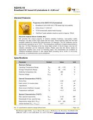
Predicting the Performance of a Photodetector - Boston Electronics ...
Predicting the Performance of a Photodetector - Boston Electronics ...
Predicting the Performance of a Photodetector - Boston Electronics ...

You also want an ePaper? Increase the reach of your titles
YUMPU automatically turns print PDFs into web optimized ePapers that Google loves.
<strong>Predicting</strong> <strong>the</strong> performance <strong>of</strong> a<br />
photodetector<br />
by Fred Perry, <strong>Boston</strong> <strong>Electronics</strong> Corporation, 91 Boylston Street, Brookline, MA 02445 USA.<br />
Comments and corrections and questions are welcome in order to insure <strong>the</strong> correctness, clarity<br />
and usefulness <strong>of</strong> this document. Phone (800)347-5445 or (617)566-3821; fax (617)731-0935;<br />
e-mail boselec@world.std.com<br />
The performance <strong>of</strong> a photodetector system can be predicted from <strong>the</strong><br />
parameters D* (detectivity), Responsivity, time constant and saturation level, and<br />
from some knowledge about <strong>the</strong> noise in <strong>the</strong> system. No photodetector should be<br />
purchased until a prediction has been made.<br />
! Detectivity and NEP<br />
The principal issue usually facing <strong>the</strong> system designer is whe<strong>the</strong>r <strong>the</strong> system<br />
will have sufficient sensitivity to detect <strong>the</strong> optical signal which is <strong>of</strong> interest.<br />
Detector manufacturers assist in making this determination by publishing <strong>the</strong><br />
figure <strong>of</strong> merit “D*”. D* is defined as follows:<br />
D*<br />
A×<br />
∆ f<br />
NEP<br />
≡ (equation 1)<br />
where A is <strong>the</strong> detector area in cm 2<br />
∆f is <strong>the</strong> signal bandwidth in hertz<br />
and NEP is an acronym for “Noise Equivalent Power”, <strong>the</strong> optical input<br />
power to <strong>the</strong> detector that produces a signal-to-noise ratio <strong>of</strong> unity (S/N=1).<br />
D* is a “figure <strong>of</strong> merit” and is invaluable in comparing one device with<br />
ano<strong>the</strong>r. The fact that S/N varies in proportion to A and ∆ f is a fundamental<br />
property <strong>of</strong> infrared photodetectors.<br />
! Active Area<br />
Consider a target about which we wish to measure some optical property. If<br />
<strong>the</strong> image <strong>of</strong> <strong>the</strong> target is larger than <strong>the</strong> photodetector, some energy from <strong>the</strong><br />
<strong>Boston</strong> <strong>Electronics</strong> Corporation, 91 Boylston Street, Brookline MA 02445<br />
(800)347-5445 or (617)566-3821 * fax (617)731-0935 * boselec@boselec.com * www.boselec.com
target falls outside <strong>the</strong> area <strong>of</strong> <strong>the</strong> detector and is lost. By increasing <strong>the</strong> detector<br />
size we can intercept more energy. Assuming <strong>the</strong> energy density at <strong>the</strong> focal plane<br />
is constant in watts/cm 2 , doubling <strong>the</strong> linear dimension <strong>of</strong> <strong>the</strong> detector means that<br />
<strong>the</strong> energy intercepted increases by 2 2 = 4 times. But NEP increases only as<br />
4 = 2 . Conversely, if <strong>the</strong> image <strong>of</strong> <strong>the</strong> target is small compared to <strong>the</strong> detector<br />
size, and if <strong>the</strong>re are no pointing issues related to making <strong>the</strong> image <strong>of</strong> <strong>the</strong> target<br />
fall on <strong>the</strong> photodetector, <strong>the</strong>n halving <strong>the</strong> linear dimension <strong>of</strong> <strong>the</strong> photodetector<br />
will similarly double S/N, since <strong>the</strong> input optical signal S stays constant while <strong>the</strong><br />
NEP DECREASES by a factor <strong>of</strong> 4 = 2 . The moral <strong>of</strong> this story is: Nei<strong>the</strong>r throw<br />
away photons nor detector area. Know your system well enough to decide on an<br />
optimized active area.<br />
! Bandwidth<br />
Error <strong>the</strong>ory tells us that signal increases in a linear fashion but noise (if it is<br />
random) adds ‘RMS’. That is, Signal increases in proportion to <strong>the</strong> time we<br />
observe <strong>the</strong> phenomenon, but Noise according to <strong>the</strong> square root <strong>of</strong> <strong>the</strong> observation<br />
time. This means that if we observe for a microsecond and achieve signal-to-noise<br />
<strong>of</strong> β, in an integration time <strong>of</strong> 100 microseconds we can expect S/N <strong>of</strong><br />
100 β = 10β . Bandwidth is related to integration time by <strong>the</strong> formula<br />
1<br />
∆f =<br />
(equation 2)<br />
2πτ<br />
where τ is <strong>the</strong> integration time or “time constant” <strong>of</strong> <strong>the</strong> system in seconds. Time<br />
constant τ is <strong>the</strong> time it takes for <strong>the</strong> detector (or <strong>the</strong> system) output to reach a value<br />
1 ⎞<br />
<strong>of</strong> 1 ≅ 63%<br />
<strong>of</strong> its final, steady state value.<br />
⎛<br />
⎜ − ⎟<br />
⎝ e ⎠<br />
! Signal<br />
Signal in all quantum photodetectors is constant versus frequency at low<br />
frequencies but begins to decline as <strong>the</strong> frequency increases. The decline is a<br />
function <strong>of</strong> <strong>the</strong> time constant. If S low is <strong>the</strong> signal at f low , a few hertz, <strong>the</strong> signal at<br />
arbitrary frequency f » f low is<br />
S<br />
low<br />
S<br />
f<br />
= (equation 3)<br />
2<br />
1+<br />
(2πτ<br />
)<br />
<strong>Boston</strong> <strong>Electronics</strong> Corporation, 91 Boylston Street, Brookline MA 02445<br />
(800)347-5445 or (617)566-3821 * fax (617)731-0935 * boselec@boselec.com * www.boselec.com
This is graphically illustrated below. Frequency f c is <strong>the</strong> point at which<br />
1<br />
S f<br />
= Slow<br />
.<br />
2<br />
! Noise<br />
Noise is not as simple as signal. Photoconductive devices like PbS, PbSe,<br />
and most HgCdTe exhibit “flicker” or 1/f noise, which is excess noise at low<br />
frequencies. Consequently, Signal-to-Noise ratio and D* are degraded at <strong>the</strong>se<br />
1<br />
frequencies. 1/f noise actually varies as in voltage terms. At high frequencies,<br />
f<br />
<strong>the</strong> detector noise actually decreases according to <strong>the</strong> same relationship as signal<br />
decreases. However, <strong>the</strong> difficulty in constructing following amplifier electronics<br />
that are significantly lower in noise than <strong>the</strong> photodetector results in system always<br />
having a noise at high frequencies that is no better than noise at low frequencies.<br />
<strong>Boston</strong> <strong>Electronics</strong> Corporation, 91 Boylston Street, Brookline MA 02445<br />
(800)347-5445 or (617)566-3821 * fax (617)731-0935 * boselec@boselec.com * www.boselec.com
The following set <strong>of</strong> graphs illustrates this.<br />
To predict low frequency performance <strong>of</strong> a photoconductor, <strong>the</strong> extent to<br />
which D* is degraded by 1/f noise must be estimated. Ei<strong>the</strong>r <strong>of</strong> <strong>the</strong> following ways<br />
is applicable:<br />
1. use <strong>the</strong> manufacturer’s published graphical data <strong>of</strong> D* versus frequency to<br />
determine <strong>the</strong> multiplication factor N excess to use to convert minimum guaranteed<br />
D* at its measured frequency to D* at <strong>the</strong> frequency <strong>of</strong> interest.<br />
2. use <strong>the</strong> 1/f “corner frequency”f corner > f low reported by <strong>the</strong> manufacturer to<br />
estimate <strong>the</strong> degradation factor at f low as<br />
excess noise factor<br />
f<br />
corner<br />
N<br />
excess<br />
= (equation 4)<br />
flow<br />
In contrast to photoconductors, photovoltaic detectors normally have no 1/f<br />
noise. Signal is flat to or near DC and <strong>the</strong>refore D* is constant below <strong>the</strong> high<br />
frequency roll-<strong>of</strong>f region, so no low frequency correction need be made.<br />
<strong>Boston</strong> <strong>Electronics</strong> Corporation, 91 Boylston Street, Brookline MA 02445<br />
(800)347-5445 or (617)566-3821 * fax (617)731-0935 * boselec@boselec.com * www.boselec.com
! Spectral response correction<br />
The D* <strong>of</strong> a quantum detector varies with wavelength λ. The detector<br />
manufacturer typically guarantees D* at <strong>the</strong> wavelength <strong>of</strong> peak response,<br />
D*(peak). When using <strong>the</strong> device at ano<strong>the</strong>r wavelength λ, <strong>the</strong> D* should be<br />
corrected by an appropriate factor:<br />
R<br />
λ<br />
=<br />
( response − at − λ)<br />
( response − at − peak)<br />
D<br />
peak<br />
×<br />
λ<br />
= D<br />
* R λ<br />
* (equation 5)<br />
where <strong>the</strong> relative response at wavelength λ is estimated by inspection <strong>of</strong> spectral<br />
response curves or o<strong>the</strong>r data supplied by <strong>the</strong> manufacturer.<br />
Therefore, <strong>the</strong> optical input power required to produce a signal-to-noise<br />
ration <strong>of</strong> 1:1 for a stated system response time and wavelength becomes:<br />
Case 1: Photoconductor at low frequency:<br />
A× ∆f<br />
NEP = ×<br />
*<br />
D<br />
λ<br />
N excess<br />
λ<br />
(equation 6)<br />
Case 2: Photovoltaic detector at low to moderate frequency:<br />
NEP<br />
λ<br />
A× ∆f<br />
= (equation 7)<br />
D<br />
*<br />
λ<br />
Case 3: Photoconductor or photovoltaic frequency at higher frequency:<br />
NEP<br />
λ<br />
S<br />
A× ∆f<br />
= (equation 8)<br />
f<br />
×<br />
D<br />
*<br />
λ<br />
This yields an estimate <strong>of</strong> <strong>the</strong> input optical power to achieve a voltage output<br />
with S/N=1.<br />
<strong>Boston</strong> <strong>Electronics</strong> Corporation, 91 Boylston Street, Brookline MA 02445<br />
(800)347-5445 or (617)566-3821 * fax (617)731-0935 * boselec@boselec.com * www.boselec.com
! Upper Limits<br />
Ano<strong>the</strong>r important question is <strong>the</strong> dynamic range <strong>of</strong> <strong>the</strong> system, e.g. <strong>the</strong> ratio<br />
<strong>of</strong> <strong>the</strong> maximum signal available to <strong>the</strong> NEP <strong>of</strong> <strong>the</strong> system. The upper limit <strong>of</strong> <strong>the</strong><br />
system is typically set by <strong>the</strong> electrical gain <strong>of</strong> <strong>the</strong> preamp or <strong>the</strong> vertical gain <strong>of</strong><br />
<strong>the</strong> oscilloscope used to display <strong>the</strong> signal, combined with <strong>the</strong> maximum output<br />
signal <strong>of</strong> <strong>the</strong> preamp or <strong>the</strong> maximum vertical deflection <strong>of</strong> <strong>the</strong> oscilloscope. The<br />
dynamic range <strong>of</strong> <strong>the</strong> system is <strong>the</strong>n expressed in multiples <strong>of</strong> <strong>the</strong> system NEP.<br />
Let <strong>the</strong> preamp gain be G. Let <strong>the</strong> responsivity <strong>of</strong> <strong>the</strong> detector in volts per<br />
watt (or volts per division in <strong>the</strong> case <strong>of</strong> an oscilloscope) at low frequency be R low<br />
and at frequency f let it be R f where<br />
R R × S<br />
f<br />
= (equation 10)<br />
low<br />
f<br />
The voltage signal from <strong>the</strong> detector into <strong>the</strong> preamp or oscilloscope when<br />
S/N=1 corresponding to this responsivity will be<br />
= (equation 11)<br />
V NEP ×<br />
f<br />
R f<br />
Then <strong>the</strong> output <strong>of</strong> <strong>the</strong> preamp at frequency f and S/N=1 will be<br />
V<br />
= V G (equation 12)<br />
preamp f<br />
×<br />
Let <strong>the</strong> maximum output <strong>of</strong> <strong>the</strong> system be Ψ preamp volts (or Ψ vertical vertical<br />
divisions in <strong>the</strong> case <strong>of</strong> an oscilloscope). The multiple <strong>of</strong> <strong>the</strong> NEP that corresponds<br />
to <strong>the</strong> maximum output Ψ preamp will <strong>the</strong>refore be<br />
Preamp Dynamic Range<br />
D<br />
Ψ<br />
preamp<br />
= (equation 13)<br />
V<br />
f<br />
× G<br />
Of course, with an oscilloscope it is usually possible to turn down <strong>the</strong> gain<br />
and thus increase <strong>the</strong> dynamic range. However, preamps usually have fixed gain.<br />
In that case <strong>the</strong> input optical must be attenuated in order to keep <strong>the</strong> output from<br />
<strong>the</strong> preamp from saturating.<br />
Sometimes <strong>the</strong> photodetector itself will saturate before <strong>the</strong> preamp. Some<br />
process, <strong>the</strong>rmal or photonic, intrinsic to <strong>the</strong> photodetector may limit it’s output.<br />
In this case, <strong>the</strong> maximum available (saturation) output signal should be specified<br />
<strong>Boston</strong> <strong>Electronics</strong> Corporation, 91 Boylston Street, Brookline MA 02445<br />
(800)347-5445 or (617)566-3821 * fax (617)731-0935 * boselec@boselec.com * www.boselec.com
y <strong>the</strong> device manufacturer, typically as a not-to-exceed output voltage Ψ detector ..<br />
Graphically <strong>the</strong> situation is illuatrated as follows:<br />
Case 1: Dynamic Range limited by <strong>the</strong> preamp<br />
D<br />
Ψ<br />
preamp det ector<br />
= <<br />
(equation 14)<br />
V<br />
f<br />
× G<br />
Ψ<br />
V<br />
f<br />
Case 2: Dynamic Range limited by <strong>the</strong> detector<br />
D<br />
Ψ<br />
V<br />
Ψ<br />
<<br />
V<br />
det ector preamp<br />
= (equation 15)<br />
f<br />
f<br />
× G<br />
This completes our prediction <strong>of</strong> system performance. We have calculated<br />
<strong>the</strong> input optical signal that corresponds to S/N=1, and <strong>the</strong> maximum output that<br />
can be extracted from <strong>the</strong> system in terms <strong>of</strong> a multiplier <strong>of</strong> <strong>the</strong> minimum input<br />
signal. The multiplier is “dynamic range”.<br />
! System options<br />
The designer has <strong>the</strong> following additional degrees <strong>of</strong> freedom in designing<br />
his system:<br />
1. He may increase <strong>the</strong> size <strong>of</strong> his optics in order to deliver more optical energy to<br />
<strong>the</strong> photodetector. The key concept to remember is that throughput in any optical<br />
system, defined asT<br />
= A× Ω , where A is area in cm 2 and Ω is solid angle field <strong>of</strong><br />
view in steradians, is a constant in <strong>the</strong> system. If A D is detector area and Ω D is<br />
<strong>Boston</strong> <strong>Electronics</strong> Corporation, 91 Boylston Street, Brookline MA 02445<br />
(800)347-5445 or (617)566-3821 * fax (617)731-0935 * boselec@boselec.com * www.boselec.com
detector FOV, <strong>the</strong>n collector area A C and collector FOV Ω C are at best satisfy<br />
AC<br />
× ΩC<br />
= T = AD<br />
× ΩD<br />
. Increasing <strong>the</strong> collector aperture decreases <strong>the</strong> FOV.<br />
2. He may increase <strong>the</strong> efficiency <strong>of</strong> his optics (transmittance and reflectance<br />
optimization, etc).<br />
3. He may increase <strong>the</strong> power <strong>of</strong> his source in a cooperative, active system<br />
(though not in a passive one).<br />
4. He may increase <strong>the</strong> time he observes <strong>the</strong> signal, that is decrease <strong>the</strong> bandwidth<br />
and increase <strong>the</strong> time constant.<br />
===========================================================<br />
Appendix 1: Sample Calculations<br />
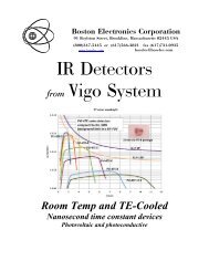
Appendix 2: D* versus wavelength and frequency for some photodetectors.<br />
<strong>Boston</strong> <strong>Electronics</strong> Corporation, 91 Boylston Street, Brookline MA 02445<br />
(800)347-5445 or (617)566-3821 * fax (617)731-0935 * boselec@boselec.com * www.boselec.com