Electron Probe Microanalysis (EPMA) - Division of Solid Mechanics
Electron Probe Microanalysis (EPMA) - Division of Solid Mechanics
Electron Probe Microanalysis (EPMA) - Division of Solid Mechanics

Create successful ePaper yourself
Turn your PDF publications into a flip-book with our unique Google optimized e-Paper software.
<strong>Electron</strong> <strong>Probe</strong> <strong>Microanalysis</strong> (<strong>EPMA</strong>)<br />
By John J. Donovan<br />
(portions from J. I. Goldstein, D. E. Newbury, P. Echlin, D. C. Joy, C. Fiori, E. Lifshin, "Scanning <strong>Electron</strong><br />
Microscopy and X-Ray <strong>Microanalysis</strong>", 2nd Ed., Plenum, New York, 1992)<br />
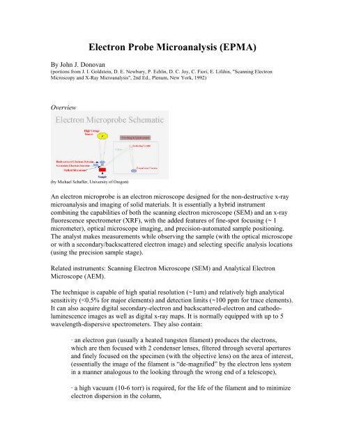
Overview<br />
(by Michael Schaffer, University <strong>of</strong> Oregon)<br />
An electron microprobe is an electron microscope designed for the non-destructive x-ray<br />
microanalysis and imaging <strong>of</strong> solid materials. It is essentially a hybrid instrument<br />
combining the capabilities <strong>of</strong> both the scanning electron microscope (SEM) and an x-ray<br />
fluorescence spectrometer (XRF), with the added features <strong>of</strong> fine-spot focusing (~ 1<br />
micrometer), optical microscope imaging, and precision-automated sample positioning.<br />
The analyst makes measurements while observing the sample (with the optical microscope<br />
or with a secondary/backscattered electron image) and selecting specific analysis locations<br />
(using the precision sample stage).<br />
Related instruments: Scanning <strong>Electron</strong> Microscope (SEM) and Analytical <strong>Electron</strong><br />
Microscope (AEM).<br />
The technique is capable <strong>of</strong> high spatial resolution (~1um) and relatively high analytical<br />
sensitivity (
· scanning coils, so the beam can raster across a specimen, producing a scanned<br />
image (a la SEM),<br />
· secondary electron detectors (which in scanning mode yield SE images, showing<br />
surface features),<br />
· backscattered electron (BSE) detectors yielding images where different phases <strong>of</strong><br />
differing mean atomic number stand out sharply,<br />
· cathodo-luminescence (CL) detectors, where the light emitted from the electronspecimen<br />
interaction can be imaged, and can clearly show features in minerals and<br />
semi-conductors that would be difficult to see compositionally (these are features<br />
due to differences in specific trace element concentrations, or crystal lattice<br />
defects)<br />
· EDS detectors which are mostly used for quick appraisal (qualitative analysis) <strong>of</strong><br />
the specimen by examining the entire x-ray spectrum, to determine the optimum<br />
analytical procedure for use with WDS<br />
Most <strong>of</strong> the periodic table can in principle be analyzed (Beryllium through Uranium),<br />
subject to several important considerations.<br />
Sample Preparation<br />
The volume sampled is typically a few cubic microns at the surface, corresponding to a<br />
weight <strong>of</strong> a few picograms and are therefore sensitive to surface contamination. Samples<br />
should be prepared as clean, flat, polished solid mounts up to 1 inch in diameter or as<br />
uncovered petrographic thin-sections, and must be stable in a 10-5 torr vacuum<br />
environment and under electron bombardment. For best results, samples must be polished<br />
to within a 0.05 um flat surface. After preparation, samples are coated with an<br />
approximately 200 Angstrom (10 nm) layer <strong>of</strong> carbon using a carbon or other conductive<br />
material in an evaporator. The use <strong>of</strong> a sputter coater which produces films <strong>of</strong> varying<br />
thickness is not used in <strong>EPMA</strong>.
What do we get from <strong>EPMA</strong>?<br />
<strong>Electron</strong> Microprobe<br />
Chemical<br />
Information<br />
Spatial<br />
Information<br />
25<br />
Cr KA1,2<br />
Cr Wavescan Counts<br />
20<br />
15<br />
10<br />
5<br />
Cr KA1<br />
Cr KA2<br />
V KB1<br />
0 V KB3<br />
V SKB''' V Cr Cr SKB'' Cr SKA4<br />
SKA3'' SKA' V SKB' V SKBN<br />
2.26 2.33<br />
Cr Angstroms<br />
Quantitative Capabilities<br />
<strong>EPMA</strong> is primarily utilized to determine the elemental composition <strong>of</strong> various materials on<br />
a micro scale. The use <strong>of</strong> standards and matrix corrections can realize accuracies <strong>of</strong><br />
typically 3-5% or better which allows the determination <strong>of</strong> many (inorganic) chemical<br />
formulas.<br />
Imaging Capabilities<br />
One may also perform digital imaging. The ability to simultaneously acquire wavelengthdispersive<br />
and energy-dispersive x-ray maps as well as secondary-electron or<br />
backscattered-electron images is <strong>of</strong>ten useful for many sample investigations.<br />
Two basic x-ray mapping modes are available, digital mapping, which is essentially a<br />
multiple-scan averaging mode that produces a binary image based on x-ray detection at<br />
each pixel (i.e. a noise suppressed dot-mapping technique), and counter-mode mapping,<br />
which is a slower pixel-by-pixel map acquisition mode with a user specified dwell time per<br />
pixel. The digital mapping and counter-mode mapping modes allow for either relatively<br />
fast acquisition with high resolution to discriminate phases with large chemical differences,<br />
and slower acquisition with low resolution to discriminate phases with smaller chemical<br />
differences, respectively.
<strong>Electron</strong> solid interactions<br />
The electron beam interacts with the specimen atoms and is significantly scattered by them<br />
as opposed to penetrating the sample in a linear fashion.<br />
When an incident electron beam interacts with the atoms in a sample, most <strong>of</strong> the energy<br />
<strong>of</strong> the electron beam will eventually end up as heat (phonon excitation <strong>of</strong> the atomic<br />
lattice), however before the electrons come to rest they primarily undergo two types <strong>of</strong><br />
scattering - elastic and inelastic.<br />
<strong>Electron</strong> scattering mechanisms:<br />
<strong>Electron</strong> <strong>Solid</strong> Interactions<br />
E e<br />
Elastic Scattering<br />
E i = E o<br />
φ e<br />
E o<br />
Inelastic Scattering<br />
E i < E o<br />
φ i
Since we are typically pushing the resolution <strong>of</strong> the instrument, it is critical to understand<br />
the size <strong>of</strong> the electron “analytical” volume (that is, the region where the x-ray are emitted<br />
from).<br />
The two trends that limit the size and shape <strong>of</strong> the interaction volume are the energy loss<br />
<strong>of</strong> the electron beam though inelastic interactions and electron loss or backscattering<br />
through elastic interactions. Specifically, the electron range is limited by the energy losses<br />
and the shape is defined by the high angle scattering <strong>of</strong> the backscattered electrons.<br />
Monte-Carlo modeling<br />
Several s<strong>of</strong>tware packages have been developed that model the scattering (elastic and<br />
inelastic) <strong>of</strong> electrons that occurs when they interact with specimens. These programs<br />
demonstrate very graphically the extent <strong>of</strong> elastic scattering that occur in bulk specimens,<br />
producing the ~micron-size "interaction volume", which is the spatial resolution <strong>of</strong><br />
chemical analysis in EMPA.<br />
from J. I. Goldstein, D. E. Newbury, P. Echlin, D. C. Joy, C. Fiori, E. Lifshin, "Scanning <strong>Electron</strong> Microscopy and X-Ray <strong>Microanalysis</strong>",<br />
2nd Ed., Plenum, New York, 1992<br />
Traditionally, textbooks show diagrams <strong>of</strong> electron scattering in a tear-shaped pattern in<br />
the specimen; this is actually a "special case", for a low atomic number plastic --<br />
appropriate for some biological material but not for higher Z materials such as minerals or<br />
metals.<br />
Interaction volumes versus beam energy
from J. I. Goldstein, D. E. Newbury, P. Echlin, D. C. Joy, C. Fiori, E. Lifshin, "Scanning <strong>Electron</strong> Microscopy and X-Ray <strong>Microanalysis</strong>",<br />
2nd Ed., Plenum, New York, 1992<br />
Interaction volumes versus atomic number
from J. I. Goldstein, D. E. Newbury, P. Echlin, D. C. Joy, C. Fiori, E. Lifshin, "Scanning <strong>Electron</strong> Microscopy and X-Ray <strong>Microanalysis</strong>",<br />
2nd Ed., Plenum, New York, 1992<br />
One can model a variety <strong>of</strong> conditions (sample thickness, accelerating voltage) on a<br />
computer prior to using an electron microbeam instrument, to determine, for example,<br />
spatial resolution <strong>of</strong> the x-ray data.<br />
X-ray production<br />
The incident electron beam traveling through the specimen may inelastically interact with<br />
the orbital electrons, as mentioned previously, to cause a displacement <strong>of</strong> the orbital<br />
electrons from their shells around nuclei <strong>of</strong> atoms comprising the sample. This interaction<br />
places the atom in an excited (unstable) state, which then seeks to return to a ground or<br />
unexcited state.<br />
<strong>Electron</strong> Energy Transition
from J. I. Goldstein, D. E. Newbury, P. Echlin, D. C. Joy, C. Fiori, E. Lifshin, "Scanning <strong>Electron</strong> Microscopy and X-Ray <strong>Microanalysis</strong>",<br />
2nd Ed., Plenum, New York, 1992<br />
There are two ways for this electron energy transition to occur, one way the energy<br />
difference is expressed is by the ejection <strong>of</strong> outer shell electrons. This is the Auger<br />
process. The other way for an atom to return to ground state is for an electron in a higher<br />
orbital to "fall" into the vacant shell and take the place <strong>of</strong> the displaced electron. When this<br />
occurs, energy is lost and a single x-ray <strong>of</strong> a narrow energy range is emitted. This is the<br />
production <strong>of</strong> characteristic x-ray radiation and it is the basis <strong>of</strong> the technique that we will<br />
be discussing.<br />
The electronic orbits <strong>of</strong> each element are relatively unique and thus the set <strong>of</strong> x-rays<br />
emitted from these electron interactions are also fairly characteristic with respect to the<br />
energy or wavelength for each element. Energy and wavelength are related by the<br />
equation,<br />
λ = 12.3985<br />
E<br />
where wavelength (lambda) is in Angstroms and energy (E) is in keV<br />
X-ray transition levels<br />
from J. I. Goldstein, D. E. Newbury, P. Echlin, D. C. Joy, C. Fiori, E. Lifshin, "Scanning <strong>Electron</strong> Microscopy and X-Ray <strong>Microanalysis</strong>",<br />
2nd Ed., Plenum, New York, 1992
For example, if an incident electron strikes an inner K shell electron and knocks it out <strong>of</strong><br />
its orbit, an L shell electron will drop into the K orbit and emit a K alpha x-ray <strong>of</strong> some<br />
diagnostic energy or wavelength; there is a lower probability that an M shell electron will<br />
drop in, yielding a K beta x-ray. Similarly, an L shell electron may be displaced by the<br />
incident electron and be replaced by an M shell, and in this case emits an L alpha x-ray.<br />
The practical result <strong>of</strong> this is that because elements <strong>of</strong> increasing Z give <strong>of</strong>f a greater<br />
variety <strong>of</strong> x-rays for they have more electrons in a greater number <strong>of</strong> orbits about their<br />
nucleus, that the lower atomic number elements have fewer lines to distribute the<br />
probability <strong>of</strong> interacting with an incident electron and hence their lines are generally are<br />
stronger in intensity, and second, the potential overlap <strong>of</strong> the greater number <strong>of</strong> peaks<br />
from higher atomic number elements constitutes the source <strong>of</strong> one potential problem in<br />
interpreting x-ray spectra.<br />
The generated characteristic x-ray intensity relates to the interaction volume because the<br />
size <strong>of</strong> this interaction volume is directly proportional to the generated x-ray intensity, that<br />
is, the greater the number <strong>of</strong> atoms excited, the greater the generated x-ray intensity, it is<br />
essential to know, if not the absolute interaction volume, then the relative interaction<br />
volume in materials <strong>of</strong> various compositions for.<br />
X-ray Detection<br />
By placing a suitable x-ray detector coupled to a set <strong>of</strong> electronic components (amplifiers,<br />
counters, analog-digital converters) and a computer, one can detect and analyze x-rays<br />
emitted from a sample undergoing electron bombardment. The resulting x-ray spectrum<br />
can be displayed according to energy (Energy Dispersive X-ray Spectroscopy - EDS) or<br />
wavelength (Wavelength Dispersive X-ray Spectroscopy -WDS). These data can then be<br />
either analyzed to give an indication <strong>of</strong> which elements occur in a sample (qualitative), or<br />
in a much more rigorous process, a precise and accurate (quantitative) chemical analysis.<br />
Energy Dispersive X-ray Analysis (EDS)<br />
X-rays emitted from a sample under electron bombardment are collected with a liquid<br />
nitrogen-cooled solid state detector<br />
EDS schematic
from J. I. Goldstein, D. E. Newbury, P. Echlin, D. C. Joy, C. Fiori, E. Lifshin, "Scanning <strong>Electron</strong> Microscopy and X-Ray <strong>Microanalysis</strong>",<br />
2nd Ed., Plenum, New York, 1992<br />
and analyzed via computer according to their energy. Typically, the computer programs<br />
used in EDS will display a real time histogram<br />
EDS spectra<br />
<strong>of</strong> number <strong>of</strong> X-rays detected per channel (variable, but usually 10 electron volts/channel)<br />
versus energy expressed in keV (thousand electron volts).<br />
In practice, EDS is most <strong>of</strong>ten used for qualitative elemental analysis, simply to determine<br />
which elements are present and their relative abundance. Depending upon the specific<br />
investigation's needs, researchers in need <strong>of</strong> quantitative results may be advised to use the<br />
electron microprobe. In some instances, however, the area <strong>of</strong> interest is simply too small<br />
and must be analyzed by TEM (where EDS is the only option) or high resolution SEM<br />
(where the low beam currents used preclude WDS, making EDS the only option).<br />
EDS Artifacts<br />
System peak, escape peaks and sum peaks, are all phenomena that an EDS user must be<br />
aware <strong>of</strong>. Modern analytical s<strong>of</strong>tware used in processing energy dispersive x-ray spectra<br />
can generally take them into account -- but such s<strong>of</strong>tware is not perfect. Also, many users<br />
will look at the raw spectra, where the s<strong>of</strong>tware may or may not have labeled the artifacts.<br />
Peak overlaps - the spectral resolution <strong>of</strong> EDS is not a great as WDS. Resolution is<br />
usually defined as the FWHM (full width at half maximum) <strong>of</strong> pure Mn Ka: ~ 150 eV.<br />
Therefore, the separation <strong>of</strong> some peaks can be poor. Examples include the case where<br />
small amounts <strong>of</strong> Fe are being investigated in the presence <strong>of</strong> large amounts <strong>of</strong> Mn (Mn<br />
Kb is very close to Fe Ka), and the case where Cu, Zn and Na are present together: the L<br />
lines <strong>of</strong> Cu and Zn are close to the K lines <strong>of</strong> Na.<br />
This figure shows the problem <strong>of</strong> attempting to analyze a Ti-V alloy with a trace amount<br />
<strong>of</strong> Cr. Because <strong>of</strong> the ubiquitous k-beta overlaps in this region <strong>of</strong> the periodic table, we<br />
have a cascade overlaps situation <strong>of</strong> a major concentration <strong>of</strong> Ti interfering with minor<br />
amount <strong>of</strong> V, which in turn significantly interferes with a trace concentration <strong>of</strong> Cr. This is<br />
a situation that definitely requires special handling to obtain quantitative results, the<br />
overlap on the trace concentration is approximately 1000%. However, much more simple<br />
and commonly encountered cases <strong>of</strong> minor spectral overlap <strong>of</strong>ten occur and the analyst is<br />
required to be aware <strong>of</strong> these difficulties.
One classic case was a paper published where Al was reported in the brains <strong>of</strong> patients<br />
with Alzheimer’s disease, but was eventually shown to be caused by the mis-identification<br />
<strong>of</strong> a minor spectral line from osmium (in osmium tetraoxide used to prepare the sample) as<br />
the Al ka line.<br />
Wavelength Dispersive Spectrometry (WDS)<br />
WDS was the original electron microprobe spectroscopy technique developed to measure<br />
precisely x-ray intensities and hence accurately determine chemical compositions <strong>of</strong><br />
microvolumes (a few cubic microns) <strong>of</strong> "thick" specimens, and the instrument used is the<br />
electron microprobe. In the 1960-70s there were roughly half a dozen companies<br />
commercially producing them; today, there are only two (JEOL and CAMECA). A fullpackage<br />
An electron microprobe today costs $500-$750,000.<br />
The key feature <strong>of</strong> the electron microprobe is a crystal-focusing spectrometer, <strong>of</strong> which<br />
there are usually 3-5, although one manufacturer in 1970-80 produced a 9 spectrometer<br />
instrument that are still much in use.<br />
WDS Schematic<br />
from J. I. Goldstein, D. E. Newbury, P. Echlin, D. C. Joy, C. Fiori, E. Lifshin, "Scanning <strong>Electron</strong> Microscopy and X-Ray <strong>Microanalysis</strong>",<br />
2nd Ed., Plenum, New York, 1992<br />
WDS focal circle figure
from J. I. Goldstein, D. E. Newbury, P. Echlin, D. C. Joy, C. Fiori, E. Lifshin, "Scanning <strong>Electron</strong> Microscopy and X-Ray <strong>Microanalysis</strong>",<br />
2nd Ed., Plenum, New York, 1992<br />
X-rays (as well as many other excited particles and radiations) are produced in the<br />
"interaction volume" immediately below the impact zone <strong>of</strong> the finely focused electron<br />
beam. A very small fraction <strong>of</strong> all x-rays will be emitted at the proper "take-<strong>of</strong>f" angle to<br />
enter the WDS spectrometer acceptance angle (a much smaller fraction compared to an<br />
EDS detector mounted a few cms from the sample). Remember each element's<br />
characteristic x-ray has a distinct wavelength, and by adjusting the tilt <strong>of</strong> the crystal in the<br />
spectrometer, at a specific angle it will diffract the wavelength <strong>of</strong> specific element's x-rays,<br />
according to Bragg’s Law:<br />
nλ<br />
= 2d<br />
sinθ<br />
Those diffracted x-rays are then directed into a gas-filled proportional counting tube,<br />
which has a thin wire (usually tungsten) running down its middle, at 1-2 kV potential. The<br />
x-rays are absorbed by gas molecules (e.g., P10: 90% Ar, 10% CH4) in the tube, with<br />
photoelectrons ejected; these produce a secondary cascade <strong>of</strong> interactions, yielding an<br />
amplification <strong>of</strong> the signal (approx. 10 6 ) so that it can be further amplified by the counting<br />
electronics.<br />
The voltage pulse produced by the incoming x-ray is accompanied by a large number (in<br />
fact an infinite number with an amplitude <strong>of</strong> zero volts) <strong>of</strong> randomly generated noise<br />
pulses <strong>of</strong> a much lower voltage. These noise pulses must be rejected before the signal is<br />
pulse counted and this is the role <strong>of</strong> pulse height analysis (PHA). Simply, special electronic<br />
circuits are adjusted so that only pulses with a certain range <strong>of</strong> energies or pulse heights<br />
(greater than the “baseline” and less than the “window”) are allowed to enter the scaler<br />
electronics for counting.
Different diffracting crystals, with 2d (lattice spacings) varying from 2.5 to 200 Å, are<br />
used to be able diffract various ranges <strong>of</strong> wavelengths that may correspond to the primary<br />
emission lines <strong>of</strong> various elements. In recent years, the development <strong>of</strong> 'layered synthetic<br />
crystals" <strong>of</strong> large 2d has lead to the ability to analyze the lower Z elements (Be, B, C, N,<br />
O), although inherent limitations in the physics <strong>of</strong> the process (e.g., large loss <strong>of</strong> signal by<br />
absorption in the sample) limit the applications.<br />
Here is a graph which illustrates the typical range <strong>of</strong> applicability for the various crystals<br />
found in many electron microprobes:<br />
Typical ranges for various analyzing crystals:<br />
80<br />
Analyzing Crystals Used in <strong>EPMA</strong> (UCB SX-51)<br />
NiCrBN<br />
60<br />
WSi60<br />
Crystal 2D<br />
40<br />
20<br />
0<br />
LiF220 LiF200 PET ADP TAP<br />
0 1 10 100<br />
Angstroms<br />
Comparison <strong>of</strong> EDS to WDS<br />
EDS can also be used to get quantitative chemical information in many situations, and the<br />
following is a comparison made at equal and optimized conditions for each method:<br />
Comparison <strong>of</strong> EDS to WDS, Equal Beam Current (from Goldstein, et. al. 1988), pure Si and Fe,<br />
10 -11 A (0.01 nA), 25 keV<br />
60 sec P (cps/10 -8 A) P/B C DL (ppm)<br />
Si Kα EDS 5400 97 580<br />
WDS 40 1513 1,710<br />
Fe Kα EDS 3000 57 1,000<br />
WDS 12 614 4,900<br />
Comparison <strong>of</strong> EDS to WDS, Optimized Conditions (from Goldstein, et. al. 1988), 15 keV, 180<br />
seconds counting time:<br />
EDS : 2 x 10 -9 A (2 nA) to give 2K cps spectrum to avoid sum peaks<br />
WDS : 3 x 10 -8 A (30 nA) to give 13K cps on Si spectrometer (> 1 % dt)<br />
Peak cps P/B C DL (ppm)<br />
EDS Na Kα 32.2 2.8 1,950<br />
Mg Kα 111.6 6.4 1,020
Al Kα 103.9 5.7 690<br />
Si Kα 623.5 22.8 720<br />
Ca Kα 169.5 8.5 850<br />
WDS Na Kα 549 83 210<br />
Mg Kα 2183 135 120<br />
Al Kα 2063 128 80<br />
Si Kα 13390 362 90<br />
Ca Kα 2415 295 90<br />
Here are some cases where WDS is the preferred technique, if available:<br />
• where greater precision is required (WDS can handle significantly higher count rates)<br />
• where the peaks are too close in EDS to be resolved (typically EDS resolution is ~150<br />
eV, versus WDS which is ~5 eV<br />
• where trace element levels are desired, WDS has a higher P/B, yielding lower<br />
minimum detection limits.<br />
WDS does not usually suffer from pulse pileup (too many counts coming in, i.e. from<br />
major elements) that occurs in EDS, and which must be compensated for mathematically.<br />
WDS has different spectral artifacts, compared with EDS: for WDS, one unique problem<br />
that may occur is if a higher order reflection (n>1) <strong>of</strong> a line falls near the line <strong>of</strong> interest<br />
and this will be discussed in the section on spectral interference below.<br />
Background correction<br />
The background correction in <strong>EPMA</strong> is required because <strong>of</strong> the production <strong>of</strong> continuum<br />
radiation from inelastic collisions by the incident electrons in the specimen. This radiation<br />
is the primary source <strong>of</strong> background in <strong>EPMA</strong> and is the limiting factor for minimum<br />
detection limits for the technique.<br />
Continuum production figure<br />
from J. I. Goldstein, D. E. Newbury, P. Echlin, D. C. Joy, C. Fiori, E. Lifshin, "Scanning <strong>Electron</strong> Microscopy and X-Ray <strong>Microanalysis</strong>",<br />
2nd Ed., Plenum, New York, 1992
Two methods are used for background correction, the most common method is the so<br />
called “<strong>of</strong>f-peak” method which measures the background due to the continuum on either<br />
side <strong>of</strong> the characteristic peak. There is also an alternative method for the correction <strong>of</strong><br />
background based on the fact that the intensity <strong>of</strong> the continuum (I c ) is a function <strong>of</strong> the<br />
mean atomic number ( Z ) <strong>of</strong> the sample.<br />
Assuming that the <strong>of</strong>f peak <strong>of</strong>fsets are appropriate and no other peaks interfere<br />
with the measurement, the intensities may be linearly interpolated and subtracted from the<br />
peak intensity. In certain cases it may be desired to utilize a measurement only on one side<br />
<strong>of</strong> the peak or to average the <strong>of</strong>f-peak measurements, however since the continuum is<br />
usually sloped and the background <strong>of</strong>fsets may not be symmetrical about the characteristic<br />
peak, care must be taken with such procedures.<br />
An example <strong>of</strong> the necessity <strong>of</strong> carefully selecting <strong>of</strong>f-peak background positions<br />
(BiPb sulfide):<br />
1500<br />
Bi Wavescan Counts<br />
1000<br />
500<br />
Pb MB<br />
Bi Bi MA1 MA2<br />
0<br />
Pb M4-O2 S S<br />
KB1<br />
SKBX Pb KB3 S Pb SMB3 Pb SKB1X SMB2 Bi SMB1 Bi Bi SMA^4 Bi SMA^3 SMA^2 SMA^1<br />
5.0 5.3<br />
Bi Angstroms<br />
An example <strong>of</strong> a curved background (MgO):<br />
634.1<br />
O Wavescan Counts<br />
0.0<br />
20000 60000<br />
O Spectrometer<br />
Peak interferences<br />
As mentioned earlier, one unique WDS spectral artifact are the higher order lines implied<br />
by Bragg’s law in which a higher energy line can diffract at the same wavelength.<br />
However, WDS can in many cases eliminate that higher order line, by fine tuning the<br />
proportional counter electronics, applying "pulse height analysis" to energy filter out the<br />
unwanted x-rays since the higher order lines, although <strong>of</strong> similar wavelength are much<br />
higher in energy. In the case <strong>of</strong> some primary (n=1) overlapping lines, even for WDS,
correction for spectral interference may be required, e.g. for V Ka in the presence <strong>of</strong><br />
abundant Ti (Kb interference) or for B Ka in the presence <strong>of</strong> abundant Mo (M-line<br />
interference).<br />
Here is an EDS spectra, <strong>of</strong> an unknown ore mineral, again acquired with a pulse<br />
processing time configured for maximum energy resolution.<br />
Ore mineral (EDS)<br />
Not a very pretty picture, since we cannot separate the Pb Lα and As Kα peaks or the Pb<br />
Mα and S kα peaks. From a qualitative viewpoint we can only state that it is at least<br />
evident that that As is present from the appearance <strong>of</strong> the As Lα line and Pb likely present<br />
from the appearance <strong>of</strong> the secondary L lines, although S is interfered strongly by the Pb<br />
Mα line and can only be inferred by the mineralogy.<br />
Here now we have the same ore mineral sample, and it's spectra acquired in the vicinity <strong>of</strong><br />
the Pb Lα and As Kα lines, using a WD spectrometer equipped with an LiF analyzing<br />
crystal with an approximate energy equivalent resolution <strong>of</strong> 10 eV.<br />
Ore mineral (WDS)<br />
5000<br />
As KA1,2<br />
Pb Wavescan Counts<br />
4000<br />
3000<br />
2000<br />
1000<br />
Pb LA1<br />
As KA2<br />
Pb LA2<br />
0<br />
1.1 1.2<br />
Pb Angstroms
As can be seen in this figure, even with the kind <strong>of</strong> resolution available with WDS, we still<br />
have large overlaps that will create confusion with qualitative analysis and much difficulty<br />
when we attempt quantitative analysis.<br />
Qualitative Analysis<br />
Qualitative analysis is the identification <strong>of</strong> the elements present in the specimen. No<br />
attempt is generally made to estimate concentrations other than major, minor, trace<br />
although even this can be difficult in many cases due to large differences in absorption<br />
between the various x-ray lines.
Quantitative analyses (Theoretical Basis)<br />
The first attempt to quantify the production <strong>of</strong> x-rays in materials was made in 1951 by<br />
Raymond Castaing, as his Ph.D. thesis at the University <strong>of</strong> Paris. Castaing proposed first,<br />
utilizing a standard along with the unknown specimen, for purpose <strong>of</strong> determining the<br />
ratio <strong>of</strong> x-ray intensities in order to eliminate calibrations pertaining to spectrometer<br />
efficiency, and second, that the ratio <strong>of</strong> those intensities could be scaled to elemental mass<br />
fraction within the specimen, seen here:<br />
ci<br />
c<br />
u<br />
s<br />
i<br />
u<br />
Ii<br />
=<br />
s<br />
(1)<br />
I<br />
i<br />
Now let’s consider, for a moment, atomic fraction averaging as a basis for modeling<br />
electron-solid interactions, which at first might seem more reasonable, although, it is<br />
evident to everyone that has worked in this area, that simple atomic fraction utterly fails to<br />
accurately describe the proportion <strong>of</strong> x-ray production contributed by the various atoms in<br />
a compound. Why is this?<br />
Figure 4<br />
In this figure, adapted from Reed (1993), we schematically depict the penetration effect <strong>of</strong><br />
the incident electron beam for a binary compound, where we have a low Z element here, a<br />
high Z element here, and in the center, a compound consisting <strong>of</strong> equal numbers <strong>of</strong> low Z<br />
and high Z atoms. It is evident, by simply comparing the number <strong>of</strong> colored circles within<br />
the interaction volumes, that the compound will contain almost as many atoms <strong>of</strong> the high<br />
Z element, as it’s pure element, but only a small fraction <strong>of</strong> the low Z element, compared<br />
to it’s pure element.<br />
Because <strong>of</strong> this disproportionality, Reed postulated that the electron beam penetrates an<br />
interaction volume <strong>of</strong> constant mass for compounds <strong>of</strong> different composition. In fact, this<br />
is only approximately true because the proportion <strong>of</strong> atomic weight (i.e., mass) to atomic<br />
number (electron interactions) or A/Z, is approximately a constant, because from isotope<br />
studies, it is known that the neutron has no effect on electron solid interactions at these<br />
energies.
In any case, a significant complication arises because we are dealing with a "thick"<br />
specimen (more than a few microns thick): absorption <strong>of</strong> X-rays, particularly long<br />
wavelength, lower energy ones, can be an important factor in reducing the number <strong>of</strong><br />
certain X-rays counted, compared to those generated in the sample.<br />
In addition to this absorption correction (A), corrections need also be made for<br />
fluorescence (F: the generated X-rays may also produce additional X-rays <strong>of</strong> other lines in<br />
the sample) and for 'atomic number effects'(Z). These three corrections are the matrix<br />
correction, ZAF, based upon various physical models developed to describe these effects,<br />
seen here:<br />
k<br />
c Z A F<br />
= (2)<br />
i i i i i<br />
Traditionally, analysts have utilized mass fraction for proportioning these inter-element<br />
effects, although as already noted above, mass is not directly involved.<br />
In the past, analysts have attempted to improve the accuracy <strong>of</strong> their analyses by selecting<br />
standards that are similar in composition to the unknowns, so that there are no large<br />
extrapolations. However, do to improvements in the algorithms used for calculation <strong>of</strong><br />
matrix effects, the use <strong>of</strong> poorly characterized standards now produce the largest errors.<br />
To avoid that, we <strong>of</strong>ten utilize, whenever possible, pure element or simple oxide standards<br />
(MgO, Al2O3, SiO2, TiO2, etc.) that have a known stoichiometric composition.<br />
Standards <strong>of</strong> this type may not always be possible to obtain (e.g., Na2O, K2O), and in<br />
those cases, and for the purposes <strong>of</strong> using secondary standards as a check on the quality <strong>of</strong><br />
the analyses, we can utilize standards whose compositions have been determined by<br />
classical wet-chemistry or other gravimetric techniques, and that similar in composition to<br />
the unknown.<br />
Absorption Correction<br />
Absorption is <strong>of</strong>ten the largest correction made to the x-ray intensities in quantitative<br />
microanalysis and therefore the accuracy with which we calculate the correction most<br />
directly influences the accuracy <strong>of</strong> the quantitative results that we may obtain. The<br />
absorption is defined as the absorption <strong>of</strong> an x-ray by the atoms present in the sample<br />
Traditionally absorption is considered a one <strong>of</strong> the terms in the ZAF correction, but within<br />
the last few decades much work has been done to describe the absorption correction as a<br />
function <strong>of</strong> the depth distribution <strong>of</strong> the generated x-rays within the sample. Therefore<br />
both factors for x-ray absorption and electron scattering (electron and energy loss) are<br />
considered at the same time. This is called the φρz curve method.<br />
In either case, the most important parameters for the correction are<br />
1. incident electron energy<br />
2. x-ray take<strong>of</strong>f angle
3. mass absorption coefficients<br />
Th incident energy <strong>of</strong> the electron beam can be determined by careful measurements <strong>of</strong> the<br />
continuum in the region where the overvoltage approaches zero also known as the Duane-<br />
Hunt limit. Use <strong>of</strong> this technique can determine the true accelerating voltage to within 50<br />
volts or so.<br />
The x-ray take-<strong>of</strong>f angle can not be directly measured except by comparison <strong>of</strong> k-ratios for<br />
opposite pairs <strong>of</strong> spectrometers.<br />
Mass absorption values which describe the photo-absorption <strong>of</strong> x-rays in the various<br />
elements have been the subject <strong>of</strong> intense experimental effort, especially for those x-ray<br />
energies equal to the emission line energies.<br />
Heinrich (CITZAF) Henke (1982)<br />
Mg Kα in Si 802 859<br />
Mg Ka in Fe 6121 5250<br />
Si Kα in Mg 2825 2902<br />
Si Kα in Fe 2502 2305<br />
As one can see there is about 20% difference in the mass absorption coefficients for Mg<br />
kα in Fe although the others are reasonably close. This difference will have a significant<br />
effect on the quantitative analysis (about 1 % or so) in this case.<br />
Atomic Number Correction<br />
The atomic number correction is used to describe electron scattering in specimens <strong>of</strong><br />
various composition. The two primary mechanisms creating the atomic number effect are<br />
changes in trajectory due to high angle scattering that cause little or no reduction in the<br />
energy <strong>of</strong> the electron (elastic scattering) and can result in a significant loss <strong>of</strong> electrons<br />
backscattered out <strong>of</strong> the sample and hence no longer involved in the production <strong>of</strong><br />
characteristic x-rays and reduction in energy <strong>of</strong> the incident electrons involved in various<br />
elastic processes such as continuum and characteristic x-ray production as well as phonon,<br />
auger, and secondary electron production.<br />
This correction may be calculated separately or combined in the φρz curve method along<br />
with the absorption correction.<br />
Fluorescence Correction<br />
The fluorescence correction is required due to the fact that not only can electrons cause x-<br />
ray fluorescence but x-rays generated by the electron beam (primary) can also cause<br />
additional x-ray fluorescence (secondary) in other elements that may also be present.<br />
The complete form <strong>of</strong> the correction (along with an analogous correction for spectral<br />
interference) is shown here:
C A<br />
u<br />
=<br />
C A<br />
s<br />
[ZAF]<br />
s<br />
lA<br />
[ZAF]<br />
u<br />
lA<br />
I u (l A<br />
)<br />
−<br />
[ZAF]<br />
s<br />
lA<br />
C B<br />
s<br />
I A<br />
s (lA )<br />
C B<br />
u<br />
[ZAF]<br />
u<br />
lA<br />
I B<br />
s (lA )<br />
Where the following notation has been adopted :<br />
j<br />
C i<br />
is the concentration <strong>of</strong> element i in matrix j<br />
[ ZAF]<br />
I i<br />
j<br />
( λ )<br />
i<br />
j<br />
λ<br />
i<br />
is the ZAF (atomic #, absorption and fluorescence) correction term for<br />
matrix j (Z and A are for wavelength λ i and F is for the characteristic line at<br />
λ i for element i)<br />
is the measured x-ray intensity excited by element i in matrix j at<br />
wavelength λ i<br />
s<br />
refers to an interference standard which contains a known quantity <strong>of</strong> the<br />
interfering element B, but none <strong>of</strong> the interfered element A<br />
Precision<br />
Precision is <strong>of</strong>ten defined as the “reproducibility” <strong>of</strong> the measurement. In other words,<br />
“what is the probability that if the measurement is repeated, we will obtain the same<br />
result”?<br />
Because the microprobe is based on x-ray counting statistics, the “significance” <strong>of</strong> the<br />
measurement is intimately related to the number <strong>of</strong> counts that we obtain. Consider that if<br />
we count for a short enough time (or at a low enough count rate), so that we obtain only<br />
a single count, the chances are roughly 50/50 that the next measurement (under the same<br />
conditions) will again produce a single count. About half the time, we will obtain no<br />
counts. So our precision error is 100%.<br />
By counting longer (and/or at higher count rates using more voltage and beam current) we<br />
will increase the total number <strong>of</strong> counts obtained and hence decrease the counting error.<br />
Because at high count rates, x-ray counting statistics can be described by essentially<br />
Gaussian statistics (low count rates are more accurately described by Poisson statistics due<br />
to the fact that we cannot measure less than zero counts), we can easily predict the<br />
precision <strong>of</strong> a measurement based simply on the total number <strong>of</strong> measured counts as<br />
shown in the following table:<br />
Precision in <strong>EPMA</strong> is related to count rate (at low to moderate cps)<br />
Total number <strong>of</strong> counts<br />
Approximate precision (assuming<br />
normal gaussian statistics)<br />
Approximate time to<br />
acquire (assuming 1K<br />
counts/sec)
100 10% 0.1 sec<br />
1,000 3.1% 1 sec<br />
10,000 1% 10 sec<br />
100,000 0.31% 100 sec<br />
1,000,000 0.1% 1000 sec<br />
Total number <strong>of</strong> counts Approximate number <strong>of</strong> significant<br />
digits (assuming 99% confidence)<br />
100
Mg Analyses<br />
“Primary” standard MgO MgO<br />
“Secondary” standard chromite diopside<br />
Measured 9.229 11.311<br />
“Published” 9.166 11.192<br />
Percent Variance 0.69 1.06<br />
Al Analyses<br />
“Secondary” standard nepheline orthoclase chromite<br />
“Primary” standard Al2O3 Al2O3 Al2O3<br />
Measured 17.607 8.379 5.181<br />
“Published” 17.868 8.849 5.250<br />
Percent Variance -1.46 -5.31 -1.32<br />
In practice, there are two ways to proceed. The first method is that by using standards as<br />
close as possible in composition to the unknown, and by assuming that the standard<br />
compositions are accurately known, because the matrix correction for an unknown that is<br />
identical in composition to the standard is exactly 1.000, we can eliminate errors due to<br />
the matrix correction itself. However, it is not always possible to find standards with<br />
similar compositions to our unknowns.<br />
The problem with this assumption is that the accuracy <strong>of</strong> the standard composition itself is<br />
not always known. While it is easy to believe that pure Si is 99.999% Si (if we can detect<br />
no trace elements) and even pure SiO2, may be said to be 99.999% SiO2, if similar in<br />
purity, it is quite a different thing to know the composition <strong>of</strong> a more complex compound<br />
that is not restricted by purity or stoichiometry (which is normally the case for a standard<br />
close in composition to our unknown).<br />
For example, an olivine standard requires that Mg, Fe and Si be known (assuming that<br />
oxygen may be calculated by stoichiometry). But because there is a solid solution from<br />
pure Fe2SiO4 to Mg2SiO4, we cannot by simple stoichiometry “know” the true<br />
composition <strong>of</strong> the olivine standard. In an attempt to determine the “true” composition <strong>of</strong><br />
Fe and Mg, it is required that these be measured independently <strong>of</strong> the microprobe. One<br />
common method is so called “classical” wet chemical methods based on gravimetric<br />
(weighing) measurements.<br />
This means that our wet chemical precision is related to the reproducibility <strong>of</strong> our<br />
weighing, mixing and diluting and the accuracy is related to the accuracy <strong>of</strong> the scale. In<br />
fact wet chemical methods have their own systematic errors that affect the accuracy <strong>of</strong> the<br />
determination <strong>of</strong> the standard composition. For example, when Al is precipitated out <strong>of</strong><br />
solution in preparation for weighing, significant Fe may also be precipitated. It is unlikely<br />
that these systematic errors in wet chemistry would cancel any systematic errors inherent<br />
in <strong>EPMA</strong> methods.
The other way to proceed with our measurements, is to utilize pure elements or simple<br />
oxides and assume that due to purity and constraints <strong>of</strong> stoichiometry (for simple oxides),<br />
that the compositions are accurately known. We then rely solely on the accuracy <strong>of</strong> the<br />
matrix corrections themselves. The accuracy <strong>of</strong> the matrix correction may be determined<br />
by careful comparison <strong>of</strong> well characterized “secondary” standards. Once again, we need<br />
to judge the accuracy <strong>of</strong> these secondary standards, but it is possible, for example, that by<br />
measuring Si Ka in a pure Mg2SiO4 against a pure SiO2 standard, we might be able to<br />
assign a confidence in how well we can matrix correction the effect Mg on Si Ka. Since<br />
both materials can be obtained pure and may be considered stoichiometric, any error in<br />
that measurement might be considered a measurement <strong>of</strong> the accuracy <strong>of</strong> the matrix<br />
correction (for that particular case at least).<br />
Trace elements<br />
Trace elements are those measurements where due to numerous factors, the signal level <strong>of</strong><br />
our measurement is similar to the measurement <strong>of</strong> the background itself.<br />
The background in the microprobe is almost entirely due to the production <strong>of</strong> continuum<br />
x-rays from the deceleration <strong>of</strong> the primary beam electrons in the sample. This presence <strong>of</strong><br />
this continuum, is the limiting factor for trace elements detection in the microprobe.<br />
To circumvent this limitation <strong>of</strong> the electron beam, some effort has been made to develop<br />
focused x-ray beams which produce much lower x-ray backgrounds. Due to the difficulty<br />
in focusing x-ray beams this still remains expensive is usually found only in large<br />
synchrotron beam lines.<br />
What signifies the detection <strong>of</strong> an element? Assuming again Gaussian statistics, it is<br />
usually stated that any measurement that exceeds 3 times the standard deviation <strong>of</strong> the<br />
background has a 99% confidence <strong>of</strong> being “real” (that is, truly present).<br />
Since the standard deviation may be described as the square root <strong>of</strong> the background<br />
counts, the calculation may be performed utilizing the formula given here, adapted from<br />
Love and Scott (1974).<br />
I<br />
CDL = ( ZAF) 3 B<br />
⋅100<br />
I t<br />
S<br />
Where : ZAF is the ZAF correction factor for the sample matrix<br />
I S is the count rate on the analytical (pure element) standard<br />
I B is the background count rate on the unknown sample<br />
t is the counting time on the unknown sample<br />
An analogous calculation which describes the analytical sensitivity <strong>of</strong> the measurement can<br />
also be calculated from similar information. The analytical sensitivity is the precision <strong>of</strong> a
measurement and allows one to assign a confidence that two measurements that differ, are<br />
in fact different.<br />
This expression, also from Love and Scott, is usually multiplied by a factor <strong>of</strong> 100 to give<br />
a percent analytical error <strong>of</strong> the net count rate.<br />
Where :<br />
N P<br />
is the total peak counts<br />
N B is the total background counts<br />
t P is the peak count time<br />
t B is the background count time<br />
Calculations based on the actual measured standard deviation <strong>of</strong> the measurement is useful<br />
for several reasons. First it allows us to determine if the variation in the measurements in<br />
due to actual variation in the sample or simply to the statistics.<br />
Secondly, once the level <strong>of</strong> homogeneity for the sample is known, we can determine the<br />
worst case analytical sensitivity since the measured standard deviation also includes<br />
variability from instrument drift, x-ray focusing, surface and coating variability.<br />
The following expressions are based on equations adapted from "Scanning <strong>Electron</strong><br />
Microscopy and X-Ray <strong>Microanalysis</strong>" by Goldstein, et. al. (Plenum Press, 1992 ed.,<br />
1981) p. 432 - 436.<br />
1. The range <strong>of</strong> homogeneity in plus or minus weight percent.<br />
W<br />
1−<br />
α<br />
= ± C t n<br />
1−<br />
α<br />
n −1<br />
1/<br />
2<br />
SC<br />
N<br />
2. The level <strong>of</strong> homogeneity in plus or minus percent <strong>of</strong> the concentration.<br />
1−<br />
α<br />
W1 −α<br />
( t<br />
± = ±<br />
n−<br />
1<br />
) SC( 100)<br />
C<br />
1/<br />
2<br />
n N<br />
3. The trace element detection limit in weight percent.<br />
C<br />
DL<br />
=<br />
N<br />
S<br />
C<br />
−<br />
S<br />
N<br />
SB<br />
/<br />
1−<br />
α<br />
2 1 2 ( t S<br />
n − 1 )<br />
1/<br />
2<br />
n<br />
C
4. The analytical sensitivity in weight percent.<br />
∆C = C − C′ ≥<br />
/<br />
1−<br />
α<br />
2 1 2 C ( t S<br />
n − 1 ) C<br />
1/<br />
2<br />
n ( N − N )<br />
B<br />
Where : C′<br />
C<br />
C s<br />
1−<br />
α<br />
t n − 1<br />
n<br />
S C<br />
N<br />
N B<br />
N S<br />
N SB<br />
is the concentration to be compared with<br />
is the actual concentration in weight percent <strong>of</strong> the sample<br />
is the actual concentration in weight percent <strong>of</strong> the standard<br />
is the Student t for a 1-α confidence and n-1 degrees <strong>of</strong> freedom<br />
is the number <strong>of</strong> data points acquired<br />
is the standard deviation <strong>of</strong> the measured values<br />
is the average number <strong>of</strong> counts on the unknown<br />
is the continuum background counts on the unknown<br />
is the average number <strong>of</strong> counts on the standard<br />
is the continuum background counts on the standard<br />
Optimal Detection Limits on the <strong>Electron</strong> Microprobe<br />
element (x-ray line) matrix voltage<br />
(KeV)<br />
current<br />
(nA)<br />
C DL<br />
(ppm)<br />
count time<br />
(sec)<br />
Al (Ka) quartz 20 100 20 640<br />
Fe (Ka) quartz 20 100 30 640<br />
Ge (Ka) Fe-Ni meteorite 35 200 20 1800<br />
C (Ka) Fe 10 50 300 1800<br />
Ca (Ka) olivine 15 200 13 2400<br />
Al (Ka olivine 15 200 18 2400<br />
Ti (Ka olivine 15 200 25 2400<br />
Cr (Ka olivine 15 200 13 2400<br />
Mn (Ka) olivine 15 200 14 2400<br />
Ni (Ka) olivine 15 200 14 2400<br />
P (Ka) olivine 15 200 14 2400<br />
Na (Ka) olivine 15 200 13 2400
Volatile element Correction<br />
Some element intensities may vary over time with exposure to the electron beam. This<br />
may be observed as either an increase or decrease in intensity over time. Since this effect is<br />
typically observed as a loss in intensity it is <strong>of</strong>ten referred to as a volatile element loss.<br />
There are several proposed mechanisms for these effects including temperature and subsurface<br />
charging. To see the effect that temperature could have on the specimen, here are<br />
some calculations for beam induced heating in various samples:<br />
Where :<br />
E i<br />
∆T = ⋅ ⎛ ⎝ ⎜ 0 ⎞<br />
4.<br />
8 ⎟<br />
kd ⎠<br />
E 0<br />
= electron beam in KeV<br />
i = beam current in uA<br />
k = thermal conductivity in watts cm-1 K-1-1<br />
d = beam diameter in um (microns)<br />
Material k DT o K (15 keV, 0.02 uA, 2 DT o K (20 keV, 0.05 uA, 2 um)<br />
um)<br />
obsidian glass 0.014 51 171<br />
zircon 0.042 17 57<br />
quartz 0.10 7.2 24<br />
calcite 0.05 14 48<br />
mica 0.006 120 400<br />
iron metal 0.80 0.9 3<br />
epoxy 0.002 360 1200<br />
This is <strong>of</strong>ten the case for volatile elements such as sodium or potassium, but the<br />
extrapolation correction can also be applied to any degradation (or enhancement) <strong>of</strong> the x-<br />
ray intensities over time due to other causes such as sample damage, carbon<br />
contamination, etc. This correction is especially useful for samples which are too small to<br />
utilize a defocused beam and allows the user to run higher sample currents to improve the<br />
analytical sensitivity.<br />
For instance, when sodium loss in observed in an alkali glass sample, a<br />
corresponding gain in silicon and aluminum x-rays may be noted. The extrapolation<br />
correction used in <strong>Probe</strong> for Windows can be applied to some or all elements in an sample,<br />
regardless <strong>of</strong> whether the x-ray intensities are decreased or increased during the<br />
acquisition (as long as the elements to be corrected are acquired as the first element<br />
on each spectrometer, i.e., order number = 1). The correction assumes that the change<br />
in counts is linear versus time when the natural LOG <strong>of</strong> the x-ray counts are plotted<br />
(Nielsen and Haraldur, 1981) as shown here :
LOG<br />
counts<br />
25<br />
20<br />
Si<br />
Na<br />
15<br />
10<br />
5<br />
0<br />
1 2 3 4 5 6 7 8 9 10 11 12<br />
Time in seconds<br />
Depending on the sample, this may or may not be a valid assumption. Under certain<br />
conditions, with very volatile hydrous alkali glasses, the change in count rate may actually<br />
decrease more quickly than a simple log decay. In this case, it may be necessary to defocus<br />
the beam slightly before acquisition.<br />
Sample Homogeneity on the Scale <strong>of</strong> the Beam Size<br />
Consider the extreme situation depicted below. An interface <strong>of</strong> Al and Cu metal where the<br />
electron beam excites x-rays from both sides <strong>of</strong> the interface.<br />
e-<br />
Al<br />
Cu<br />
In this situation, x-rays <strong>of</strong> both metals will be produced. However, note that because the<br />
Cu x-rays are generated mostly in a pure Cu matrix and the Al x-rays are mostly generated<br />
in an pure Al matrix, the actual matrix correction that needs to be applied to the measured<br />
x-rays will be different than simply the matrix correction for a homogenous alloy sample<br />
consisting <strong>of</strong> both Al and Cu.<br />
Now, as you may know, the matrix correction for the x-ray <strong>of</strong> an element in the pure<br />
element is considered to be 1.0. Hence for the majority <strong>of</strong> the x-rays produced in this<br />
sample, the matrix correction that needs to be applied to each x-ray is very close to 1.0<br />
since, as stated above, most <strong>of</strong> the Cu x-rays are generated in a pure Cu matrix and most<br />
<strong>of</strong> the Al x-rays are generated in a pure Al matrix. However, when the microprobe<br />
measures the x-ray intensities at this boundary and receives both Al and Cu x-rays, it<br />
knows nothing <strong>of</strong> the actual geometry, and can only assume that all the x-rays measured<br />
are to be matrix corrected using a composition that is determined by iteratively correcting<br />
the measured x-ray intensities. This is the nature <strong>of</strong> the ZAF or phi-rho-z matrix<br />
correction. Of course, one could apply a geometric model to the matrix correction to
correct for the interface effect, but this would require precise knowledge <strong>of</strong> the interface<br />
shape and orientation which is usually not available.<br />
Since determining the geometry <strong>of</strong> a buried interface is difficult if not impossible,<br />
the s<strong>of</strong>tware can only assume a matrix correction based on a composition consisting <strong>of</strong><br />
both Cu and Al, since both x-rays were detected. The matrix correction for Al x-rays in a<br />
homogenous Cu-Al alloy is <strong>of</strong> course quite different than that <strong>of</strong> pure Al, which is really<br />
the situation that created the Al x-rays in our example and the same is true for the Cu x-<br />
rays as well. The effect <strong>of</strong> assuming a homogenous matrix, when in fact the sample is very<br />
inhomogenous, is to apply the wrong matrix correction to the x-rays detected from the<br />
sample.<br />
The following is a calculation for the correction <strong>of</strong> Cu kα and Al kα x-rays in a<br />
50:50 homogenous alloy at 15kV and a 52.5 degrees take<strong>of</strong>f angle :<br />
50:50 Cu-Al alloy Cu Al<br />
Elemental k-ratio 0.45732 0.34037<br />
ZAF correction 1.0933 1.4690<br />
As you can see, the correction for both x-rays, but especially Al kα (47% ZAF<br />
correction), is significantly higher than the correction for each x-ray in the pure element<br />
(1.0). This will result in a very high total as the beam straddles the interface between the<br />
two phases, since both x-rays will be over corrected by homogenous alloy composition<br />
matrix correction. This example is extreme, but the situation applies to any inhomogenous<br />
sample in which the matrix correction for the different phases present are not equal. This is<br />
because the matrix correction itself is non-linear and cannot be applied to the normalized<br />
x-ray intensities generated from the different phases.<br />
It is best to remember the words <strong>of</strong> the late Chuck Fiori, who said : "if the feature is<br />
smaller than the size <strong>of</strong> the beam, then all bets are <strong>of</strong>f".<br />
It is also important to remember that when the sample inhomogeneity is much smaller than<br />
the scale <strong>of</strong> the beam (for example particle phases less than 0.05 microns), that this effect<br />
becomes insignificant due to the fact that the many phases involved in the production and<br />
absorption <strong>of</strong> the x-rays tend to average out the contribution from a single phase. Of<br />
course this also means that it is possible to only determine the average composition <strong>of</strong><br />
very fine grained materials. But at least we don't have to worry about inhomogeneity on<br />
the atomic scale!<br />
Sample preparation<br />
Poor sample preparation- rough surfaces can preferentially bias the analysis against low<br />
energy x-ray as seen in this figure,<br />
Rough surface figure
Rough surface problems:<br />
Conductive coatings (if any) must be carefully applied to clean surfaces and is required to<br />
be <strong>of</strong> the same composition and thickness for both the standard and the unknown sample.<br />
In many cases, (light element analysis) this may require that the standards and unknowns<br />
be coated at the same time.<br />
Problems with sample geometry<br />
Tilted sample problems:<br />
Line <strong>of</strong> sight problems:<br />
Incorrect sample geometry - X-rays emerge from a sample and travel line - <strong>of</strong> -sight<br />
trajectories. Thus, if the sample is tilted incorrectly, something may actually block the path<br />
between detector and sample.<br />
This will manifest itself either as an inordinately low number <strong>of</strong> X-rays (expressed as<br />
counts sec-1) or you may notice an absence <strong>of</strong> low energy X-rays (either due to blocking<br />
or re-absorption) in the spectrum being collected. This is not normally a concern on the<br />
microprobe where specimens are polished flat, although it can occur when the analyzed<br />
area is near the edge <strong>of</strong> the mounted sample as seen in the above figure.<br />
Carbon coat thickness variation
Variations in the thickness <strong>of</strong> the carbon (or other conductor) coat, can result in a<br />
difference in intensity emitted from the specimen surface. This may result from two<br />
different mechanisms.<br />
In the first, s<strong>of</strong>t x-ray emitted from the sample are absorbed by the coating, hence if the<br />
absorption is significant enough, then differences in the thickness <strong>of</strong> the coating between<br />
the standard and the unknown will produce a difference in the intensity <strong>of</strong> the x-ray<br />
detected from the sample and standards. Due to the non-linear and complex nature <strong>of</strong> the<br />
absorption (absorption edges) it is not possible to make a general statement regarding the<br />
magnitude <strong>of</strong> the effect. The following table gives several examples for absorption <strong>of</strong><br />
several commonly measured s<strong>of</strong>t x-rays in carbon coats <strong>of</strong> three different thicknesses:<br />
Percent x-ray transmission (assume density <strong>of</strong> carbon is 2.7 gm/cm3):<br />
10 nm (carbon) 20 nm (carbon) 40 nm (carbon)<br />
Ti Kα (19.76) 0.99994 0.99989 0.99978<br />
Si Kα (356.8) 0.99903 0.99807 0.99615<br />
Al Kα (557.2) 0.99849 0.99699 0.99400<br />
Mg Kα (904.8) 0.99756 0.99512 0.99027<br />
Na Kα (1534) 0.99586 0.99175 0.98356<br />
F Kα (6366) 0.98295 0.96620 0.93355<br />
O Kα (12,380) 0.96712 0.93533 0.87484<br />
N Kα (25,490) 0.93349 0.87140 0.75935<br />
Another way in which the carbon coat can affect the emitted intensities is due to the<br />
absorption <strong>of</strong> the primary beam electrons in the coating. This slowing down <strong>of</strong> the primary<br />
electrons results in an effective loss in energy <strong>of</strong> the incident electrons. For x-rays with a<br />
high overvoltage this reduction in primary beam energy is negligible, but for elements with<br />
an over voltage closer to 1.5 to 2 (for example Fe Ka at 10 KeV), this could affect the<br />
generated intensity calculation significantly.
Appendix A: Timeline <strong>of</strong> <strong>Electron</strong> Microscopy and X-ray <strong>Microanalysis</strong><br />
1895 - X-rays discovered by Roentgen, produced by electron bombardment <strong>of</strong> inert gas in<br />
tubes; gas fluoresces and nearby photographic plates are exposed (X-rays' wavelength =<br />
0.05 - 100 Å)<br />
1898 - Starke in Berlin found backscatter intensity varies with Z<br />
1909 - term "characteristic x-rays" first used by Barkla and Sadler but the physical origin<br />
<strong>of</strong> x-rays not clear and Kaye built an cathode ray tube with an ionization chamber to detect<br />
x-rays<br />
1912 - Von Laue, Friedrich and Knipping confirmed that X-rays could be diffracted by<br />
crystals with lattice spacings <strong>of</strong> similar dimension<br />
1913 - the Bohr model <strong>of</strong> the atom explained the characteristic x-ray spectra and Bragg<br />
obtained the first X-ray spectrum <strong>of</strong> Pt using an NaCl crystal (Bragg’s Law: n*lamda = 2d<br />
*sin theta )<br />
1913 - Mosely found that there was a systematic variation <strong>of</strong> the wavelength <strong>of</strong><br />
characteristic X-rays from various elements ( wavelength inversely proportional to Z<br />
squared )<br />
λ =<br />
B<br />
( Z − C) 2<br />
where B and C are constants for each characteristic line family and Z is the atomic<br />
number.<br />
1922 - Hadding used X-ray spectra to chemically analyze minerals<br />
1923 - von Hevesy discovered Hf after noticing a gap at Z=72<br />
late 1920's - in Germany, development <strong>of</strong> transmission electron microscopes, with first<br />
demonstration in 1932 <strong>of</strong> transmission electron microscopy by Ernst Ruska<br />
(belated Nobel prize for it in 1986) prototype build by Siemens & Halske Co but WWII<br />
prevented sale and use outside Germany<br />
1930's - scanning coils added to TEM, producing STEM (image produced by secondary<br />
electrons emitted by specimen)<br />
1940 - RCA sold first commercial TEM outside Germany<br />
1942 - first use <strong>of</strong> SEM to examine surfaces <strong>of</strong> thick specimens at RCA Labs
1949 - Castaing built first electron microprobe for microchemical analysis (with crystal<br />
focusing wavelength dispersive spectrometer = WDS) for Ph.D at University<br />
<strong>of</strong> Paris, and developed the basic theory<br />
1956 - commercial production <strong>of</strong> electron microprobe began (Cameca)<br />
1965 - commercial production <strong>of</strong> SEM began<br />
1968 - solid state EDS detectors developed
Useful References<br />
J. T. Armstrong, "Quantitative analysis <strong>of</strong> silicates and oxide minerals: Comparison <strong>of</strong> Monte-Carlo, ZAF<br />
and Phi-Rho-Z procedures," Microbeam Analysis--1988, p 239-246.<br />
J. T. Armstrong, "Bence-Albee after 20 years: Review <strong>of</strong> the Accuracy <strong>of</strong> a-factor Correction Procedures<br />
for Oxide and Silicate Minerals," Microbeam Analysis--1988, p 469-476.<br />
G. F. Bastin and H. J. M. Heijligers, "Quantitative <strong>Electron</strong> <strong>Probe</strong> <strong>Microanalysis</strong> <strong>of</strong> Carbon in Binary<br />
Carbides," Parts I and II, X-Ray Spectr. 15: 135-150, 1986<br />
J. J. Donovan, D. A. Snyder and M. L. Rivers, "An Improved Interference Correction for Trace Element<br />
Analysis" Microbeam Analysis, 2: 23-28, 1993<br />
J. J. Donovan and T. N. Tingle, "An Improved Mean Atomic Number Correction for Quantitative<br />
<strong>Microanalysis</strong>" in Journal <strong>of</strong> Microscopy, v. 2, 1, p. 1-7, 1996<br />
J. I. Goldstein, D. E. Newbury, P. Echlin, D. C. Joy, C. Fiori, E. Lifshin, "Scanning <strong>Electron</strong> Microscopy<br />
and X-Ray <strong>Microanalysis</strong>", Plenum, New York, 1981<br />
J. I. Goldstein, D. E. Newbury, P. Echlin, D. C. Joy, C. Fiori, E. Lifshin, "Scanning <strong>Electron</strong> Microscopy<br />
and X-Ray <strong>Microanalysis</strong>", 2nd Ed., Plenum, New York, 1992<br />
K. F. J. Heinrich, "Mass Absorption Coefficients for <strong>Electron</strong> <strong>Probe</strong> <strong>Microanalysis</strong>" in Proc. 11th<br />
ICXOM 67: 1, 1982.<br />
McQuire, A. V., Francis, C. A., Dyar, M. D., "Mineral standards for electron microprobe analysis <strong>of</strong><br />
oxygen", Am. Mineral., 77, 1992, p. 1087-1091.<br />
Nielsen, C. H. and Sigurdsson, H., "Quantitative methods for electron microprobe analysis <strong>of</strong> sodium in<br />
natural and synthetic glasses", Am. Mineral., 66, p. 547-552, 1981<br />
J. L. Pouchou and F. M. A. Pichoir, "Determination <strong>of</strong> Mass Absorption Coefficients for S<strong>of</strong>t X-Rays by<br />
use <strong>of</strong> the <strong>Electron</strong> Microprobe" Microbeam Analysis, Ed. D. E. Newbury, San Francisco Press, 1988, p.<br />
319-324.<br />
S. J. B. Reed, <strong>Electron</strong> <strong>Probe</strong> Analysis, 2nd ed., Cambridge University Press, Cambridge, 1993<br />
V. D. Scott and G. Love, "Quantitative <strong>Electron</strong>-<strong>Probe</strong> <strong>Microanalysis</strong>", Wiley & Sons, New York, 1983<br />
K. G. Snetsinger, T. E. Bunch and K. Keil, "<strong>Electron</strong> Microprobe Analysis <strong>of</strong> Vanadium in the Presence<br />
<strong>of</strong> Titanium", Am. Mineral., v. 53, (1968) p. 1770-1773