Owens Design Introduces High Speed Automation Platform for PV ...
Owens Design Introduces High Speed Automation Platform for PV ...
Owens Design Introduces High Speed Automation Platform for PV ...
Create successful ePaper yourself
Turn your PDF publications into a flip-book with our unique Google optimized e-Paper software.
Press Release<br />
For Immediate Release<br />
1 P.M. EDT, Oct. 5, 2009<br />
Contact Mark Danna | 510.659.1800<br />
mdanna@owensdesign.com<br />
<strong>Owens</strong> <strong>Design</strong> <strong>Introduces</strong> <strong>High</strong> <strong>Speed</strong> <strong>Automation</strong><br />
<strong>Plat<strong>for</strong>m</strong> <strong>for</strong> <strong>PV</strong> Wafer Inspection Applications<br />
<strong>PV</strong> Wafer Handling Module combines Industry-Leading Throughput with<br />
low Breakage Rate<br />
Fremont, Cali<strong>for</strong>nia: <strong>Owens</strong> <strong>Design</strong> Inc., a leading equipment design and build service<br />
provider to the solar, semiconductor, and data storage capital equipment markets, today<br />
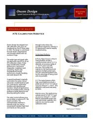
introduced a c-Si Inspection <strong>Automation</strong> <strong>Plat<strong>for</strong>m</strong> optimized <strong>for</strong> use with productionvolume,<br />
high-speed photovoltaic (<strong>PV</strong>) wafer inspection applications. The <strong>Owens</strong> c-Si<br />
Inspection <strong>Automation</strong> <strong>Plat<strong>for</strong>m</strong> provides high speed, high reliability wafer handling in<br />
customizable configurations to meet advanced factory automation requirements. Input<br />
load modules can be configured <strong>for</strong> either cassette or coin stack input while the output<br />
sorter module can be expanded from 6 to 18 output bins. Available <strong>for</strong> either 125mm x<br />
125mm (5 inch) or 156mm x 156 mm (6 inch) <strong>PV</strong> wafers, <strong>Owens</strong> c-Si automation<br />
plat<strong>for</strong>m delivers an industry-leading throughput of 3600 wafers per hour, coupled with a<br />
low breakage rate of less than 0.2 percent. <strong>Design</strong>ed to be customizable to the specific<br />
requirements of any <strong>PV</strong> inspection tool, the module is ideal <strong>for</strong> volume-production<br />
applications.<br />
“We developed the c-Si automation plat<strong>for</strong>m to enable our OEM solar customers to<br />
rapidly introduce their wafer inspection technology into high volume solar fabs,” said<br />
John Apgar, <strong>Owens</strong> <strong>Design</strong>’s President. “The inspection of <strong>PV</strong> wafers is an important<br />
step in maximizing yield <strong>for</strong> outgoing and incoming quality assurance. This automation<br />
plat<strong>for</strong>m allows our customers to focus on their inspection technology while depending<br />
on us to provide high wafer throughput at a very low breakage rate; both of which are of<br />
critical importance to the solar fab.”<br />
To learn more about the c-Si Inspection <strong>Automation</strong> <strong>Plat<strong>for</strong>m</strong> or more about <strong>Owens</strong><br />
<strong>Design</strong> visit us at Solar Power International 2011, Booth 4842, at the Dallas Convention<br />
Center, October 18-20.<br />
<strong>Owens</strong> <strong>Design</strong> offers capital equipment manufacturers a proven methodology to reduce<br />
tool development costs, minimize technical risk and speed their time to market. By
working closely with an established design and build services company, such as <strong>Owens</strong><br />
<strong>Design</strong>, a capital equipment company can focus its internal ef<strong>for</strong>ts on its core<br />
technology. In turn, <strong>Owens</strong> <strong>Design</strong> can focus on integrating this core technology into a<br />
system level plat<strong>for</strong>m that has been optimized to meet the equipment manufacturer’s<br />
per<strong>for</strong>mance specifications.<br />
For more in<strong>for</strong>mation about <strong>Owens</strong> <strong>Design</strong>’s products and services, please visit<br />
www.owensdesign.com.<br />
About <strong>Owens</strong> <strong>Design</strong><br />
— End —<br />
<strong>Owens</strong> <strong>Design</strong> specializes in engineering and manufacturing of capital equipment. Located<br />
in Silicon Valley <strong>for</strong> over 25 years, they have been a strategic partner in the co-creation and<br />
manufacturing process <strong>for</strong> many leading OEM capital equipment companies. <strong>Owens</strong><br />
<strong>Design</strong> engineers and manufactures customer's products from concept, through alpha,<br />
beta, pilot and on-going production. Their development process results in a rapid design<br />
cycle and concurrent manufacturing introduction. <strong>Owens</strong> <strong>Design</strong> has and continues to be<br />
an innovative and reliable partner <strong>for</strong> equipment companies in the semiconductor, solar<br />
and related industries.


