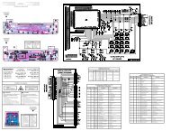
CAM350 V 6.0 : Plot Separate Sheet - sch-8000-3.pcb - Reptips
CAM350 V 6.0 : Plot Separate Sheet - sch-8000-3.pcb - Reptips
CAM350 V 6.0 : Plot Separate Sheet - sch-8000-3.pcb - Reptips

Create successful ePaper yourself
Turn your PDF publications into a flip-book with our unique Google optimized e-Paper software.
Service Manual<br />
___________________________________________________________________________________<br />
Chassis Professional <strong>8000</strong><br />
___________________________________________________________________________________<br />
Service notes<br />
After a repair the cables must be laid out as originally fitted to save compliance with original approval<br />
and to avoid failures or disturbances.<br />
The mains cable prevents interference from the mains supply and is part of the product approval. For<br />
replacement the original spare part only must be used.<br />
Note di servizio<br />
Dopo una riparazione i cavi devono essere disposti come posizionati all’origine per mantenere la<br />
corrispondenza con le approvazioni originali ed evitare guasti o disturbi.<br />
Il cavo di alimentazione previene interferenze provenienti dalla rete elettrica ed è parte delle<br />
approvazioni del prodotto. Per la sostituzione deve essere utilizzato esclusivamente il ricambio<br />
originale.<br />
Modifications reserved - Con riserva di modifiche
Service procedure for Chassis Professional <strong>8000</strong><br />
Power supply<br />
Adjust PP1 for 140 V +/- 0.5 V across CP37.<br />
Entering service mode<br />
1. Turn on the appliance at the mains switch while holding down the MENU key on the<br />
local control until the red LED lights up.<br />
2. Release the MENU key on the local control and press the stand-by key on the remote<br />
control. The appliance will start up in service mode with a specific support menu.<br />
3. The various functions can be selected using the P+ and P- keys on the remote control<br />
and the adjustment can be made using the Volume + keys. It is advisable to make a note of<br />
the initial value before making the adjustment so that it can easily be restored if necessary.<br />
If the memory NVM (ICR3) is replaced, it is essential to carry out all the adjustments<br />
required in service mode because the replacement memory is supplied NOT preprogrammed.<br />
If the EPROM (ICR2) containing the software is replaced, compatibility with<br />
the existing NVM is verified automatically and if necessary it is initialised. These<br />
operations may take some time, so you must wait until they are completed.<br />
Although the individual settings can be accessed and memorised individually and<br />
independently, it is advisable to carry them out in the sequence in which they appear<br />
when pressing the P- key.<br />
Option byte<br />
The correct value to be set for each appliance is marked on the label on the back of each item<br />
alongside the writing Option byte. The value can be entered using the number keys on the<br />
remote control.<br />
AFC setting<br />
Connect a generator (or a known transmitter of reliable quality) to the antenna input and use<br />
the remote control number keys to enter the value of its RF frequency (which must be within<br />
the frequency band indicated by the menu), then press OK. The setting will be made<br />
automatically.<br />
Repeat the procedure for BG, L and L’ standards. If any of the settings are omitted, operation,<br />
automatic search and tuning in this standard may be incorrect.<br />
AGC tuner setting<br />
Connect a generator with an RF level of 1 mV (60 dBµV) (or a known transmitter of reliable<br />
quality) to the antenna input and use the remote control number keys to enter the value of its<br />
frequency (which must be within the frequency band indicated by the menu), then press OK.<br />
The setting will be made automatically.<br />
Screen grid voltage (Vg2)<br />
Adjust the potentiometer G2 on the transformer EHT until the confirmation message appears.<br />
No particular signal set-up is required.<br />
Vertical geometry<br />
The VS (Vertical Slope) function must be adjusted in such a way that the central horizontal<br />
line in the test signal is exactly on the border between the visible image and the lower black<br />
part. It must not subsequently be altered.<br />
Now set the remaining parameters as accurately as possible in the sequence in which they<br />
appear.
Horizontal geometry<br />
Adjust as accurately as possible in the sequence in which they appear.<br />
Adjusting white (Red/Green)<br />
Using a B/W bar signal, adjust to obtain a grey image. The blue setting is fixed.<br />
Exiting service mode<br />
Once you have made the necessary adjustments, press the OK key on the remote control in<br />
one of the menus in which it is active to memorise all the functions and return to normal<br />
operation of the appliance.
Oscillograms Chassis Professional <strong>8000</strong> (1/5)<br />
0 V<br />
0 V<br />
0 V<br />
1 1 V/Div 10 µs/Div<br />
2 1 V/Div 10 µs/Div<br />
3 1 V/Div 10 µs/Div<br />
0 V<br />
0 V 0 V<br />
4 20 V/Div 10 µs/Div 5 20 V/Div 10 µs/Div 6 20 V/Div 10 µs/Div<br />
0 V 0 V<br />
0 V<br />
7 100 V/Div 5 µs/Div 8 5 V/Div 5 µs/Div<br />
9 100 V/Div 5 µs/Div<br />
0 V<br />
10 500 mV/Div 5 µs/Div<br />
0 V<br />
11 2 V/Div 5 µs/Div 12 100 V/Div 5 µs/Div<br />
0 V<br />
0 V<br />
0 V<br />
13 2 V/Div 10 µs/Div 14 500 mV/Div 10 µs/Div<br />
0 V<br />
15 1 V/Div 5 ms/Div<br />
1
Oscillograms Chassis Professional <strong>8000</strong> (2/5)<br />
0 V<br />
0 V<br />
0 V<br />
16 1 V/Div 10 µs/Div<br />
17 5 V/Div 10 µs/Div<br />
18 2 V/Div 10 µs/Div<br />
0 V 0 V<br />
19 200 V/Div 10 µs/Div<br />
20 5 V/Div 5 ms/Div 21 50 V/Div 10 µs/Div<br />
0 V<br />
0 V<br />
0 V<br />
0 V<br />
22 50 V/Div 5 ms/Div 23 10 V/Div 5 ms/Div<br />
24 10 V/Div 10 µs/Div<br />
0 V<br />
0 V<br />
25 50 V/Div 10 µs/Div<br />
0 V<br />
26 50 V/Div 5 ms/Div<br />
27 50 V/Div 10 µs/Div<br />
0 V<br />
0 V<br />
0 V<br />
28 5 V/Div 10 µs/Div<br />
29 1 V/Div 10 µs/Div<br />
30 1 V/Div 10 µs/Div<br />
2
Oscillograms Chassis Professional <strong>8000</strong> (3/5)<br />
0 V<br />
0 V<br />
0 V<br />
31 1 V/Div 10 µs/Div<br />
32 500 mV/Div 10 µs/Div<br />
33 500 mV/Div 10 µs/Div<br />
0 V<br />
0 V<br />
0 V<br />
34 500 mV/Div 10 µs/Div<br />
35 1 V/Div 10 µs/Div<br />
36 1 V/Div 5 ms/Div<br />
0 V<br />
0 V<br />
0 V<br />
37 1 V/Div 5 ms/Div<br />
38 2 V/Div 10 µs/Div 39 1 V/Div 10 µs/Div<br />
0 V<br />
40 2 V/Div 10 µs/Div<br />
0 V<br />
41 200 mV/Div 50 ns/Div<br />
0 V<br />
42 2 V/Div 10 µs/Div<br />
0 V<br />
0 V<br />
0 V<br />
43 500 mV/Div 10 µs/Div 44 1 V/Div 20 µs/Div<br />
45 1 V/Div 20 µs/Div<br />
3
Oscillograms Chassis Professional <strong>8000</strong> (4/5)<br />
0 V<br />
46 1 V/Div 5 ms/Div<br />
0 V<br />
47 500 mV/Div 20 µs/Div<br />
0 V<br />
48 500 mV/Div 20 µs/Div<br />
0 V<br />
49 500 mV/Div 20 µs/Div<br />
0 V<br />
50 500 mV/Div 20 µs/Div<br />
0 V<br />
51 500 mV/Div 20 µs/Div<br />
0 V<br />
52 1 V/Div 20 µs/Div<br />
0 V<br />
53 500 mV/Div 10 µs/Div<br />
0 V<br />
54 500 mV/Div 10 µs/Div<br />
0 V<br />
55 500 mV/Div 10 µs/Div<br />
0 V<br />
56 500 mV/Div 20 µs/Div<br />
0 V<br />
57 500 mV/Div 20 µs/Div<br />
0 V<br />
58 500 mV/Div 20 µs/Div<br />
0 V<br />
59 1 V/Div 20 µs/Div<br />
0 V<br />
60 1 V/Div 5 ms/Div<br />
4
Oscillograms Chassis Professional <strong>8000</strong> (5/5)<br />
0 V<br />
0 V<br />
0 V<br />
61 1 V/Div 10 µs/Div<br />
62 1 V/Div 5 ms/Div<br />
63 1 V/Div 10 µs/Div<br />
0 V<br />
64 1 V/Div 5 ms/Div<br />
5
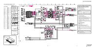
Chassis Professional <strong>8000</strong><br />
Circuit description<br />
Modifications reserved - Aenderungen vorbehalten - Con riserva di modifiche<br />
1
Power supply<br />
Consists of two completely separate sections:<br />
• Stand-by power supply<br />
• Main power supply<br />
Stand-by power supply<br />
This is an SMPS (Switch Mode Power Supply) operating at about 50 kHz with primary<br />
side control and stabilisation performed by the integrated circuit VIPer20A (ICP10), which<br />
provides exclusively the voltages required by the appliance in stand-by mode.<br />
In these conditions the main power supply is completely deactivated, which allows for an<br />
exceptionally low overall consumption (< 1 W), far lower than even the most stringent<br />
standards.<br />
The transformer TRP2 performs the dual function of isolating the appliance from the<br />
mains power supply and generating on the secondary winding the supply voltage + 5 Vsb<br />
which powers the IR receiver (IRH1), the microcontroller (ICR1), the NVM memory (ICR3),<br />
the reset circuit (ICR6) and the EPROM (ICR2) containing the software. A duplicator<br />
circuit is used to obtain a voltage of about 20 V used for turning off the electromagnetic<br />
mains switch (optional).<br />
Main power supply<br />
This is an SMPS (Switch Mode Power Supply) operating at about 45 kHz with secondary<br />
side control and stabilisation performed by the integrated circuit TEA2262 (ICP1).<br />
The transformer TRP1 performs the dual function of isolating the appliance from the<br />
mains power supply and generating the correct supply voltages on the various secondary<br />
windings.<br />
In stand-by the TRIAC DP2 does not conduct, so the circuit (including the PTC powering<br />
the degaussing coil) is completely disconnected from the power supply and therefore has<br />
no power consumption.<br />
When it is turned on by means of the photo-coupler ICP3, the TRIAC DP2 is made to<br />
conduct and the rectified and smoothed mains voltage across CP14, via winding 5/2 of<br />
transformer TRP1, is present on the collector of TP1, which does not conduct because<br />
ICP1 is not yet powered.<br />
Simultaneously CP16 is charged from mains via RP3. As soon as the voltage across it<br />
reaches a value of about 10 V, the integrated circuit begins to operate and generates on<br />
pin 14 the driving pulses for making transistor TP1 conduct.<br />
Current therefore begins to flow in the primary winding 5/2 of the transformer and across<br />
the winding 1/7 there are formed pulses which are rectified by DP4 and smoothed by<br />
CP16 and ensure a complete power supply of ICP1.<br />
At the same time currents are also induced in the secondary windings; after being rectified<br />
and smoothed these currents generate the various power supply voltages.<br />
A voltage taken from across CP37 by way of the voltage divider made up of<br />
RP35/RP29/RP23/RP33/PP1 is applied to the base of TP4 and causes a proportional<br />
current to flow in the photodiode contained in the optocoupler ICP2.<br />
2
This value is transferred via the photo-coupler emitter to the input (pin 6 of ICP1) of a<br />
comparator which regulates the duration of the base drive pulses of transistor TP1.<br />
This controls the time for which current is allowed to flow in the primary winding (and<br />
therefore regulates the energy fed into the transformer) and gives extremely precise<br />
stabilisation of the voltages available on the transformer’s secondary windings.<br />
The circuit made up of CP24/CP25/LP10/DP6 controls the current harmonics towards the<br />
mains power supply and may be present or absent depending on applicable regulations.<br />
This solution activates automatic demagnetisation of the CRT every time the appliance is<br />
turned on, not just from the switch but also from stand-by. This solves the problem of<br />
possible purity degradation if the appliance (as often happens) is not turned off regularly<br />
from the mains switch.<br />
Protection<br />
To protect against supply voltage variations, the integrated circuit ICP1 interrupts<br />
generation of driving pulses to pin 14 if the voltage at pin 16 is higher than about 15.5 V.<br />
Furthermore the current that flows in the transistor TP1 is read across RP9 and is applied<br />
to pin 3 via RP5/RP14; if it exceeds the maximum permitted value, the driving pulses to<br />
pin 14 are interrupted.<br />
This protects the transistor TP1 and safeguards against short-circuits in the transformer’s<br />
secondary windings.<br />
Microcontroller<br />
A latest-generation device with 16-bit architecture (ICR1 - M30612SFP) is used,<br />
supported by an EPROM (Electrically Programmable Read Only Memory) that contains all<br />
the appliance software.<br />
The various functions are controlled either by changing the logic state (L or H) of some<br />
pins on the microcontroller or by way of a two-wire digital bus (pins 27/28) designated IICbus<br />
(Inter Integrated Circuit Bus).<br />
An additional IIC-bus (pins 91/92) is devoted exclusively to dialoguing with the NVM<br />
memory (Non Volatile Memory) (ICR3) to provide maximum protection against data<br />
corruption.<br />
Connected to pins 32/33/34 there is also a special high-speed M3-L bus dedicated<br />
exclusively to dialoguing with ICR5 (SDA5273-2P) for managing teletext and graphic<br />
OSDs (On Screen Displays).<br />
The signal from the IR receiver is applied to pin 7 of the microcontroller, which begins its<br />
activity when the supply voltage is present and the reset cycle (active L) at pin 12 has<br />
been completed.<br />
For this reason if the system shows abnormal behaviour it is important to turn the power<br />
switch off and back on again to generate a reset pulse allowing the program to be<br />
reinitialised.<br />
3
When the reset pulse has terminated, the microcontroller waits until the control signals<br />
from IR are present at pin 7 or those from the local control are present at pin 97.<br />
Execution of the entire program is timed by the clock signal generated by the 10 MHz<br />
crystal and applied to pins 13/15.<br />
A valid command for exiting standby generates a level L at output pin 100, thereby<br />
enabling powering up of all the circuits as described in the power supply section.<br />
The microcontroller first verifies that the power supply has come on correctly by checking<br />
that pin 18 (START) is at level H, then all the possible peripherals are interrogated via the<br />
IIC-Bus to recognise the configuration of the appliance and thereby structure the program.<br />
All data regarding the operating parameters required for correct setting of all the functions<br />
(tuning, analogue values, geometries, option bytes, etc.) are subsequently called up from<br />
the memory ICR3.<br />
The various functions are carried out and commands given primarily via the digital buses.<br />
The functions of the remaining microcontroller pins are described below:<br />
Pin 1 - Output (LPW) which goes to level L during the main power supply start-up to<br />
activate initial operation of the horizontal deflection stage.<br />
Pins 3/4 - DAC (Digital to Analog Converter) outputs for headphone volume and balance<br />
control.<br />
Pin 19 – Input connected to vertical flyback pulse used for managing communication<br />
timing with 100 Hz processor.<br />
Pin 20 – Output which goes to level H to activate audio power amplifier muting.<br />
Pin 21 – Output for controlling satellite antenna system switching.<br />
Pins 24/25 – Inputs for automatically recognising the configuration of the 100 Hz<br />
conversion system.<br />
Pin 26 – Input for automatically recognising correspondence of deflection hardware used.<br />
Pin 30 – Input for automatically recognising the presence of the Comb filter.<br />
Pins 35/36/37 – Outputs reserved for future use.<br />
Pin 38 – Output for controlling loudspeaker configuration in Dolby Pro Logic mode.<br />
Pin 89 – Input used for controlling VGA input enabling.<br />
Pin 93 – Output for controlling illumination of local control LED.<br />
Pin 94 – Output for controlling activation of electromagnetic switch (if present).<br />
Pin 95 – Input connected internally to an ADC (Analog to Digital Converter) to measure<br />
the value of the tuner’s AGC voltage.<br />
4
Pin 97 – Input connected internally to an ADC (Analog to Digital Converter) to measure<br />
the value of the voltage generated by the local control keys and hence discriminating the<br />
control.<br />
Note that the software also identifies the configuration of the appliance by way of an<br />
option code contained in the memory ICR3. This option code must therefore be checked<br />
and if necessary adjusted if ICR3 is replaced. The correct value for each model is marked<br />
on the label on the back of each item after the words “option code”. It can be set by<br />
entering service mode (follow the necessary safety procedures).<br />
In this mode it is also possible to make all the adjustments for the various calibrations<br />
under the control of a specific program contained in the microcontroller, which also verifies<br />
automatically whether NVM data initialisation operations are required.<br />
NVM memory (ICR3)<br />
This is an EEPROM (Electrically Erasable Programmable Read Only Memory) NVM (Non<br />
Volatile Memory) with a 16K bit capacity and an IIC-bus interface.<br />
The microcontroller writes and reads all the variable data relevant to operation in the<br />
memory.<br />
In addition to user option data (tuning, analogue levels, etc.), memory ICR3 also contains<br />
data regarding the settings of many of the appliance’s functions, such as geometries,<br />
option bytes, white level adjustment, etc.<br />
If the memory is replaced, these settings must be restored through the appropriate<br />
service procedures.<br />
However, the program contains special check routines so the appliance can be turned on<br />
when the memory is not programmed or even not present, thereby simplifying the service<br />
procedures.<br />
Video signal processing / deflection<br />
The various items of information in the video signal are processed by the integrated<br />
circuits TDA9321H (ICC2), TDA9332H (ICC1) and SAA4977H (ICY1).<br />
• TDA9321H<br />
5
Video<br />
The IF signal from the tuner whose band is limited by the surface wave filter FCC5 is<br />
routed to pins 2/3, which are connected to the input of the video demodulator<br />
(synchronous PLL type with active carrier regeneration). This assures ultralinear<br />
demodulation, an excellent demodulation figure, a low harmonic content and an excellent<br />
impulsive response.<br />
The only residual adjustment that must be carried out on the video demodulation circuits<br />
is tuning of coil LC9 of the VCO oscillator and setting the working point of the tuner AGC,<br />
which is controlled by way of pin 62. Both the adjustments are performed fully<br />
automatically by the software in service mode.<br />
The baseband video signal is available with an amplitude of 2 Vpp at pin 10 and is applied<br />
via the audio carrier suppression filter FCC3 to pin 12, which represents the input of the<br />
group delay correction circuit controlled by software.<br />
After this treatment the signal is available at pin 13 with an amplitude of 2 Vpp.<br />
From here it is sent both to the SCART 1 output and to one of the video selector inputs<br />
(pin 14) after being taken to the level of 1 Vpp.<br />
Further video inputs are available at pins 16 (AV1), 18 (SAT), 20 (AV2) and 23 (FRONT).<br />
S-VHS sources whose chrominance signals are connected to pins 21 and 24 can also be<br />
connected to the AV2 and FRONT inputs respectively.<br />
The video signal of the selected source is taken from pin 26 to power the teletext decoder.<br />
In order to send the selected signal to the screen, it is routed internally through a bandpass<br />
filter to remove the chrominance signal and a trap to eliminate the colour subcarrier<br />
from the luminance signal.<br />
In the case of SVHS sources these circuits are bypassed.<br />
Switched capacitance circuits are also included for creating luminance delay lines.<br />
The chrominance signal is demodulated in accordance with the PAL/SECAM/NTSC<br />
standard identified automatically and with the aid of integrated delay lines. The carrier<br />
reconstruction oscillators are connected to their respective crystals via pins 54 and 57.<br />
Original spare parts must be used for these components as all the functions of the<br />
integrated circuit take their frequencies as reference.<br />
After the treatments described above, the luminance signal Y50 and the colour difference<br />
signals U50, V50 are available on pins 49, 50 and 51 respectively.<br />
There are also two video outputs which can be freely connected to any of the inputs and<br />
are used for the SCART2 output (pin 34) and for the PIP module (pin 32).<br />
Pins 25, 26, 27, 28, 29 and 30 are used for connection to an optional comb-filter. The<br />
SCART1 RGB input is connected to pins 40, 41, 42 and 43 and the PIP source Y/U/V<br />
signals to pin 36, 37, 38, 39.<br />
Pins 19 and 22 are outputs which can be placed in an H or L level under the control of the<br />
software and are used respectively for L/L’ switching of the audio filter FCC4 and for<br />
switching of the video signal output on SCART1 by means of the transistors TW3, TW4,<br />
TW5, TW6, TW7 and TW8.<br />
Audio<br />
The IF signal from the tuner whose band is limited by the surface wave filter FCC4 is<br />
routed to pins 63/64, which are connected to the mixer consisting of a multiplier which<br />
6
converts the IF signal to the intercarrier frequency. This frequency is available at pin 5<br />
after a high-pass filter which eliminates the video content.<br />
The is also an AM audio demodulator whose output is also connected to pin 5.<br />
Deflection<br />
The horizontal and vertical synchronising signals are extracted from the screen video<br />
signal.<br />
The horizontal synchronising pulse HA is available at pin 60, the vertical synchronising<br />
pulse VA at pin 61 and the sandcastle pulse at pin 59.<br />
• SAA4977H (1fH / 2fH converter)<br />
The signals Y50, U50, V50 coming from ICC2 are connected to input pins 26, 28 and 30,<br />
while the horizontal HA and vertical VA synchronising signals are connected to pins 22<br />
and 20 respectively.<br />
To double the field frequency (100 Hz) it is necessary to write the same original field twice<br />
on the screen.<br />
For this purpose, the incoming video signals are first digitalised by sampling them at 8 bits<br />
and then transferred to a memory (ICY4), from which they are read at double speed.<br />
Digital to analog reconversion is then performed and the double-frequency analog signals<br />
are available at pins 79, 76 and 74. The circuits formed by TY1/TY2, TY3/TY4 and<br />
TY5/TY6 adapt the levels for the ICC1 inputs.<br />
It is also necessary to generate the HD/VD synchronising pulses at double frequency and<br />
synchronous to those of the original HA/VA signal.<br />
This is done with the help of the PLL circuit made up of ICY2 and ICY3.<br />
All checks and signals needed for the various functions and for memory management are<br />
inside ICY1, which also contains a microcontroller and resident software to carry out the<br />
various activities. The transistors TY8/TY9 form the reset circuit for this microcontroller.<br />
The integrated circuit ICY9 switches the synchronising signals between the internal<br />
source (pins 2 and 5) and the VGA input (pins 3 and 6). Switching is controlled by pin 3 of<br />
ICY1.<br />
The integrated circuit ICY5 (if present) increases the definition by acting on the signal’s<br />
transient fronts.<br />
• TDA9332H<br />
Video<br />
Signals Y100, U100 and V100 from the 100Hz conversion module are connected to pins<br />
26, 27 and 28.<br />
The RGB signals for performing saturation, contrast and brightness controls are restored<br />
by way of the matrix circuits. The signals for driving the video final amplifiers are therefore<br />
available on output pins 40, 41 and 42.<br />
Pin 44 is the input for the measurement pulses for adjusting the cut-off, which uses an<br />
automatic system for alignment at both low and high current, thereby optimising the<br />
7
performance of the tube. Adjustment of voltage Vg2 is fully automated in service mode by<br />
a special software procedure.<br />
Pin 43 is the control input for automatic limitation of the tube current.<br />
Pins 35, 36, 37 and 38 are the inputs of the RGB signals for the OSD and teletext, while<br />
pins 30, 31, 32 and 33 are the RGB inputs of the VGA source. These inputs require<br />
sources with a horizontal frequency of 32 kHz.<br />
Deflection<br />
The entire management of the deflection controls refers to the 12 MHz oscillator FCC1<br />
connected to pins 20/21.<br />
When turned on, the transistor TC3 is made to conduct by pin 1 of microcontroller ICR1,<br />
thereby powering pin 22. This activates the output of horizontal driving pulses from pin 8<br />
at a frequency of about 50 kHz. This starts the horizontal deflection stage, whose<br />
consumption permits stabilisation of the power supply.<br />
When the power supply voltage on pins 17/39 reaches 8V, the horizontal driving output<br />
progressively switches to its rated frequency (32 kHz) and the steady-state operating<br />
mode is reached. The software now disconnects the power supply voltage from pin 22.<br />
The transistor TC4 is normally inhibited because its base, via RC34, is connected to earth<br />
by the jumper JF1 situated on the power supply/deflection circuit and this level L is also<br />
carried to pin 26 of the microcontroller. This also allows the correct operating frequency of<br />
ICC1 (H = 32 kHz; L = 15 kHz) to be provided via pin 12, which also depends on the<br />
deflection hardware used.<br />
The horizontal HD and vertical VD synchronising pulses are applied to input pin 24 and 23<br />
respectively.<br />
Pin 13 is the input of the horizontal flyback pulse and pin 4 is the input for dimensional<br />
stabilisation of the image as the tube current varies.<br />
Pin 9 is used as input to protect the tube, blancking it out in the event of a fault in the<br />
vertical deflection circuits.<br />
Pins 1 and 2 are the symmetrical outputs for vertical driving and pin 3 is the output for<br />
E/W correction control.<br />
All the adjustments are performed in service mode by a special support software program.<br />
Video final amplifiers<br />
The RGB signals available at pins 40/41/42 on ICC1 (TDA9332H) must be amplified and<br />
inverted in order to reach the level required for driving the CRT.<br />
The integrated circuit TDA6108 (ICV1) is used for this purpose.<br />
The final amplifier inputs are connected to pins 1/2/3 and the outputs (pins 7/8/19) are<br />
connected directly to the CRT’s cathodes via the protection resistors RV5/RV7/RV10.<br />
A copy of the currents flowing in the CRT’s cathodes are available at pin 5 and this<br />
information is sent to the video processor TDA9332H for automatic cut-off control circuit<br />
operation.<br />
8
Transistors TV1 and TV4 form a circuit which serves to eliminate CRT spot formation when<br />
the appliance is turned off.<br />
During operation the heater’s supply pulses, which are rectified and filtered by DV6 and CV6,<br />
keep TV1 saturated and hence inhibit TV4.<br />
The capacitor CV19 is therefore able to charge up at the voltage of +200V by way of RV19<br />
and DV10. Grids 1 (G1) of the tube remain at ground potential since DV10 is conducting.<br />
As soon as the appliance is turned off, the final line stage stops providing the heater’s power<br />
supply pulses; TV1 is inhibited and TV4 is saturated by the +200V voltage still present and<br />
applied at its base via RV18.<br />
The collector of TV4 grounds the positive armature of CV19. As a result, grids 1 of the CRT<br />
are polarised with the negative 200V voltage present on its negative armature since the diode<br />
DV10 is now polarised the other way round.<br />
This way the CRT is completely inhibited for the time it takes CV19 to di<strong>sch</strong>arge, thus<br />
preventing spot formation.<br />
The RGB signals, decoupled by means of the transistors TV7/TV8/TV9, are added<br />
together and transferred to the power stage made up of TV5 and TV6 by means of the<br />
circuit made up of TV2 and TV3. The coupling capacitor CV13 together with the power<br />
stage input impedance forms a differentiator circuit which generates pulses of suitable<br />
polarity upon each signal transition. This drives a special deflection coil on the CRT which<br />
modulates the deflection velocity (Beam Velocity Modulation), thereby significantly<br />
improving image definition.<br />
Horizontal deflection<br />
The output line transistor is driven by the transformer TRL1 whose primary winding is<br />
driven by the transistor TL1, connected to the horizontal drive output of ICC1 via the<br />
emitter-follower TC5.<br />
The horizontal deflection stage is carried out in a conventional manner with the deflection<br />
transistor TL2, the diode (DL4/DL5) EW modulation circuit and pin-cushion distortion<br />
correction (CL8/LL6). The correction signal EW is injected into the central point of the<br />
diodes via LG2.<br />
The capacitive divider formed by CL11/CL12 is used for picking up the horizontal flyback<br />
pulse to be applied to pin 13 of ICC1, limiting its maximum value to 8V by means of the<br />
diode DL11.<br />
Vertical deflection – EW correction<br />
9
These functions are performed by the integrated circuit TDA8351 (ICF1). This is a power<br />
amplifier with a bridge output that allows the vertical deflection coils to be connected<br />
directly to pins 4 and 7. The resistances RF9/RF10, which provide pin 9 with the<br />
necessary feedback signal, are placed in series.<br />
The differential input circuit (pins 1/2) is driven by the voltage formed across RF3/RF4 for<br />
the symmetrical driving currents provided by ICC1.<br />
Pin 8 is an output which switches to the value H at vertical flyback. This signal is<br />
connected to pin 9 of ICC1 and is used to protect the CRT in the event of failure of the<br />
vertical deflection circuits.<br />
Two separate supply voltages are used for the deflection part (pin 3) and for generating<br />
the flyback pulse (pin 6), thereby achieving a high value of efficiency.<br />
The power stage for EW correction consists of transistor TG1 which is driven directly by<br />
ICC1 and whose collector is connected to the injection coil LG2 by means of RG4.<br />
Audio signal processing<br />
The various audio functions are treated by the circuits TDA9870/5A (ICS1), SAA7710T<br />
(ICS4), TDA7467D (ICS5), TDA2616 (ICS2/ICS6), TDA7053AT (ICS3).<br />
• TDA 9870A / TDA 9875A<br />
The integrated circuits have the same basic functions: the version TDA9875A additionally<br />
contains a complete NICAM digital audio decoder.<br />
The audio IF signal from pin 5 of ICC2 is applied to input pin 12. The AM audio signal (in<br />
the case of L/L’ standard) is also extracted by way of the transistor TS1 and the low-pass<br />
filter formed by RS34 and CS13 and is taken to input pin 29. A second IF input (pin 10) is<br />
used for the audio signal of the satellite receiver (if present).<br />
All audio functions (demodulation, stereo/NICAM decoding, input/output switching,<br />
volume/tone control, effects) for BG/DK/I/LL’ standards are contained in the integrated<br />
circuit and are totally selected and controlled via software.<br />
The audio inputs from the SCART 1 and SCART 2 sockets are connected to pins 33/34<br />
and 36/37 respectively, while the audio input from the front RCA sockets (optional) is<br />
connected to pins 31/32.<br />
10
Pins 47/48 and 51/52 are the outputs towards the SCART 1 and SCART 2 sockets<br />
respectively.<br />
Pins 62/63 are the constant level outputs for the LINE OUT sockets, fed by the transistors<br />
TW11 and TW13; pins 60/61 are the outputs for the loudspeaker power amplifiers (ICS2).<br />
Pins 22/23/25/26/27 are the inputs/outputs of the I2S digital bus used for communications<br />
with ICS4 (present only in Dolby Pro Logic appliances).<br />
• SAA 7710T<br />
This is present only in appliances equipped with Dolby Pro Logic decoding and also<br />
provides the function of a 5-band audio equaliser.<br />
Signal treatment is fully digital and data transfer to and from ICS1 is performed via the bus<br />
I2S which is connected to pins 22/23/24/28/29.<br />
A specific software program is responsible for complete management of all functions,<br />
including a special spatial sound (Incredible Sound) which offers effects similar to Pro<br />
Logic decoding without the need to install rear loudspeakers.<br />
• TDA 7467D<br />
ICS5 can be used as an alternative to the Dolby Pro Logic decoder ICS4. This creates<br />
special spatial sound effects while using solely the loudspeakers contained in the<br />
appliance.<br />
The input signal to be processed is connected to the pins 2/3 and the outputs are<br />
connected to pins 1/28. It is fully managed by software.<br />
• TDA 2616<br />
This is a double Hi-Fi audio power amplifier in accordance with DIN45500.<br />
ICS2 is always present, whereas ICS6 is used solely in Dolby Pro Logic appliances to<br />
amplify the central and rear channels.<br />
The input signals are connected to pins 1/9 and the outputs to pins 4/6.<br />
Pin 2 mutes the amplifiers and is controlled via the transistor TW9.<br />
The transistors TW12 and TW14 activate MUTE during power supply transients.<br />
The right and left channel signals are also added together and sent, via the transistor<br />
TW10, to the woofer box amplifier (present in some models only).<br />
• TDA 7053AT<br />
This is a double amplifier used to power the headphone socket.<br />
The inputs are connected to pins 4/6 and the outputs to pins 9/16. The reproduced signal<br />
is the same as that of the loudspeakers and its volume and balance can be controlled by<br />
way of pins 2/8 connected to the output pins 3/4 of microcontroller ICR1.<br />
11
Woofer amplifier<br />
This is present in some models only and is used to power the woofer loudspeaker box.<br />
The integrated circuit LM358N (ICB1A/B) constitutes a two-stage low-pass filter in<br />
cascade and serves to eliminate all frequencies higher than about 300 Hz from the audio<br />
signal spectrum.<br />
Power amplification is performed by the integrated circuit TDA2616 (ICB2) connected in a<br />
bridge configuration, which directly powers the box loudspeaker.<br />
The circuit made up of the transistor TB2 and the relay RLB1 is used solely in Dolby Pro<br />
Logic appliances to adapt the internal loudspeaker connections according to the<br />
installation configuration chosen by the user from the OSD menu.<br />
Switching is managed by pin 38 of the microcontroller, which directly drives the base of<br />
TB2.<br />
VGA interface<br />
This option (present only on some models) allows the appliance to be used as a computer<br />
monitor at the following VGA resolutions only:<br />
pixel horizontal vertical<br />
640x480 31.5 kHz 60 Hz<br />
640x350 31.5 kHz 70 Hz<br />
640x400 31.5 kHz 70 Hz<br />
The PC’s graphic interface must be set for these resolutions.<br />
The RGB video signals are sent directly to the input pins 30/31/32 of ICC1 while the<br />
synchronising signals from pins 13 and 14 of CNM1 are applied to the integrated circuit<br />
ICM1 (Quad.2-input exclusive-OR) which provides positive pulses to output pins 3/6<br />
whatever the input polarity. This way the appliance is automatically adapted to any type of<br />
PC.<br />
The presence of horizontal and vertical synchronising pulses is checked by means of<br />
ICM2, whose output pins 6 and 10 are at level H only if the horizontal and vertical<br />
synchronising pulses respectively are present.<br />
Only in this case can pin 2 of CNM3 (VGA ENABLE) go to level H.<br />
The integrated circuit ICM3 is used to check that the frequency of the horizontal<br />
synchronising pulses is lower than the maximum value set by PM1 to prevent an incorrect<br />
PC resolution setting damaging the television’s horizontal deflection stages.<br />
Potentiometer PM1 is factory-set. It requires special equipment for adjustment and<br />
its setting must not be altered.<br />
12
If the value of the horizontal frequency is not correct, pin 10 of ICM3 is kept at level L and<br />
consequently the communication line with the microcontroller (VGA ENABLE) goes to<br />
about 2.5 V. This information is used to generate a specific error message.<br />
The integrated circuit ICM4 switches between VGA and front RCA audio sources and the<br />
transistors TM1/TM2/TM3/TM4 adapt the VGA audio level to that inside the TV set.<br />
13
Spare parts list<br />
Lista parti di ricambio Chassis Professional <strong>8000</strong><br />
Rev 1.2<br />
Ref./pos<br />
Part.No.<br />
Codice<br />
Description Descrizione NOTE<br />
S00055<strong>8000</strong> Front End PCB <strong>8000</strong> cpl. Base Front End <strong>8000</strong> cpl.<br />
S000558750 Front End PCB <strong>8000</strong> Nicam/Dolby cpl. Base Front End <strong>8000</strong> Nicam/Dolby cpl.<br />
S000558500 Front End PCB <strong>8000</strong> Nicam cpl. Base Front End <strong>8000</strong> Nicam cpl.<br />
S000558250 Front End PCB <strong>8000</strong> Dolby cpl. Base Front End <strong>8000</strong> Dolby cpl.<br />
! S047501000 Fusible resistor 1 Ohm Resistenza sicurezza 1 Ohm<br />
! S047502200 Fusible resistor 2,2 Ohm Resistenza sicurezza 2,2 Ohm<br />
! S047504700 Fusible resistor 4,7 Ohm Resistenza sicurezza 4,7 Ohm<br />
RW46 S055408020 Wire wound resistor 1 Ohm 7W Resistenza a filo 1 Ohm 7W<br />
S061112050 Diode BAS 32 L Diodo BAS 32 L<br />
DC4/DC5 S061517920 Diode BA792/T1 Diodo BA792/T1<br />
ZC4 S061518100 Diode BAS81 Diodo BAS81<br />
ZR1 S061703300 Zener diode 3V3 Diodo zener 3V3<br />
ZC3 S061706800 Zener diode 6V8 Diodo zener 6V8<br />
ZC5 S061713300 Zener diode 33V Diodo zener 33V<br />
S062608500 Transistor BC 847 B Transistor BC 847 B<br />
S062608600 Transistor BC 857 B Transistor BC 857 B<br />
ICS2/ICS6 S063126160 I.C. TDA 2616/N1 I.C. TDA 2616/N1<br />
ICS1 S063198700 I.C. TDA 9870A (no Nicam) I.C. TDA 9870A (no Nicam)<br />
ICS1 S063198750 I.C. TDA9875A V2 (Nicam) I.C. TDA 9875A V2 (Nicam)<br />
ICR3 S063286160 I.C. EEPROM M24C16-BN6 I.C. EEPROM M24C16-BN6<br />
ICR2 S063342700 I.C. EPROM M27C4001-80XF1 I.C. EPROM M27C4001-80XF1<br />
ICR4 S063344400 I.C. MSM514400D-60 I.C. MSM514400D-60<br />
ICR1 S063362060 I.C. M30612SFP I.C. M30612SFP<br />
ICR6 S063363190 I.C. M51953BFP I.C. M51953BFP<br />
ICS4 S063377100 I.C. SAA 7710T/N104/T3 (Pro Logic only) I.C. SAA 7710T/N104/T3 (Pro Logic solo)<br />
ICR5 S063552730 I.C. SDA 5273 2P I.C. SDA 5273 2P<br />
ICS3 S063570530 I.C. TDA 7053AT/N2,118 I.C. TDA 7053AT/N2,118<br />
ICC2 S063593200 I.C. TDA 9321H/N1/T3 I.C. TDA 9321H/N1/T3<br />
ICC1 S063593310 I.C. TDA 9332H/N1/T3 1Y I.C. TDA 9332H/N1/T3 1Y<br />
ICC1 S020030000 I.C. TDA 9332H/N2/T3 2Y I.C. TDA 9332H/N2/T3 2Y<br />
QC4 S066900150 Quarz 3,58 Mhz Quarzo 3,58 Mhz<br />
QC1 S066900250 Quarz 4,43 Mhz Quarzo 4,43 Mhz<br />
QR1 S066900400 Quarz 10 Mhz Quarzo 10 Mhz<br />
QR2 S066902040 Quarz 20,48 Mhz Quarzo 20,48 Mhz<br />
QS1 S066902450 Quarz 24,576 Mhz Quarzo 24,576 Mhz<br />
Pagina 1
QS2 S066903680 Quarz 36,864 Mhz Quarz 36,864 Mhz<br />
FCC5 S067322000 SAW Filter K3953M Filtro SAW K3953M<br />
FCC4 S067322500 SAW Filter K9453M Filtro SAW K9453M<br />
FCC1 S067330610 Ceramic resonator CSTCS 12.0MT Risuonatore ceramico CSTCS 12.0MT<br />
FCC3 S067401050 Ceramic filter TPS 5,5 MWA Filtro ceramico TPS 5,5 MWA<br />
LC9 S067408200 Coil P3691NAS-A41 Bobina P3691NAS-A41<br />
TUC1 S069023200 Tuner UV 1316 AI2 Tuner UV 1316 AI2<br />
PLS1/PLS2 S071013400 Ext. Speaker connector Presa x altop. esterno<br />
SC1/SC2 S071014800 Double SCART connector Presa SCART doppia<br />
CNS6 S071015400 Line out RCA connector Presa RCA line out<br />
S087170000 Chassis holder side Staffa supporto telaio<br />
S087178100 Chassis rear connector cover Sfondo posteriore<br />
S087178500 Chassis holder front Supporto telaio anteriore<br />
S000568500 Power PCB <strong>8000</strong> 4:3 25" PH cpl. Modulo Power <strong>8000</strong> 4:3 25" PH cpl.<br />
S000568510 Power PCB <strong>8000</strong> 4:3 28" PH cpl. Modulo Power <strong>8000</strong> 4:3 28" PH cpl.<br />
S000568520 Power PCB <strong>8000</strong> 4:3 29" PH cpl. Modulo Power <strong>8000</strong> 4:3 29" PH cpl.<br />
S000568530 Power PCB <strong>8000</strong> 4:3 34" VI cpl. Modulo Power <strong>8000</strong> 4:3 34" VI cpl.<br />
S000568800 Power PCB <strong>8000</strong> 16:9 28" VI cpl. Modulo Power <strong>8000</strong> 16:9 28" VI cpl.<br />
S000568810 Power PCB <strong>8000</strong> 16:9 32" VI cpl. Modulo Power <strong>8000</strong> 16:9 32" VI cpl.<br />
S000568820 Power PCB <strong>8000</strong> 16:9 28" PH cpl. Modulo Power <strong>8000</strong> 16:9 28" PH cpl.<br />
! S044010100 Fusible resistor 1 Ohm NFR25 Resistenza sicurezza 1 Ohm NFR25<br />
! S044010470 Fusible resistor 4,7 Ohm NFR25 Resistenza sicurezza 4,7 Ohm NFR25<br />
! S048002200 Fusible resistor 2,2 Ohm NFR25H Resistenza sicurezza 2,2 Ohm NFR25H<br />
! S048033000 Fusible resistor 33 Ohm NFR25H Resistenza sicurezza 33 Ohm NFR25H<br />
! S048147000 Fusible resistor 470 Ohm NFR25H Resistenza sicurezza 470 Ohm NFR25H<br />
RP1 ! S053051000 Safety resistor 1MOhm VR37 Resistenza 1 MOhm VR37<br />
RP38 ! S053210700 Safety resistor 4M7Ohm VR68 Resistenza 4M7 Ohm VR68<br />
RP9 S054000150 Wire wound resistor 0,15 Ohm 3W Resistenza a filo 0,15 Ohm 3W<br />
S054001000 Resistor 1 Ohm 2W Resistenza 1 Ohm 2W<br />
S054004700 Resistor 4,7 Ohm 2W Resistenza 4,7 Ohm 2W<br />
RF11 S054115000 Resistor 150 Ohm 2W Resistenza 150 Ohm 2W<br />
RP3 S054347000 Resistor 47 KOhm 2W Resistenza 47 KOhm 2W<br />
RP16 S055492270 Resistor 27 KOhm 7W Resistenza 27 KOhm 7W<br />
NTC1 S056590200 NTC resistor 4,7 Ohm Resistenza NTC 4,7 Ohm<br />
PTC1 ! S056591100 PTC resistor 12A Resistenza PTC 12A<br />
S061002100 Diode BAV 21/A52A Diodo BAV 21/A52A<br />
DF1 S061111320 Diode 1N 4007 Diodo 1N 4007<br />
S061112050 Diode BAS 32L Diodo BAS 32L<br />
S061281050 Diode BAV 203-GS18 Diodo BAV 203-GS18<br />
S061301360 Diode BYW 36 Diodo BYW 36<br />
S061401370 Diode BYD 37K/T1 Diodo BYD 37K/T1<br />
S061503750 Diode BYD37J,115 Diodo BYD37J,115<br />
Pagina 2
DP16/DP24 S061706200 Zener diode 6V2 Diodo zener 6V2<br />
ZF1/ZL1 S061909350 Zener diode BZT03-C51/A52A Diodo zener BZT03-C51/A52A<br />
ZP1 S061703300 Zener diode 3V3 Diodo zener 3V3<br />
DP20 S061011000 Bridge rectifier B250D Diodo ponte B250D<br />
DP1 S061270000 Bridge rectifier B380C3200-2200 Diodo ponte B380C3200-2200<br />
DP10 S061299080 Diode BYW 80PI-200 Diodo BYW 80PI-200<br />
DP5/DP8 S061299120 Diode BYT 12PI-1000 Diodo BYT 12PI-1000<br />
S061303800 Diode BYV 98-200 Diodo BYV 98-200<br />
DL10 S061316870 Diode BY 228 Diodo BY 228<br />
DL5 S061316900 Diode BY 229F-800 Diodo BY 229F-800<br />
DL4 S061319200 Diode BY 459X-1500 Diodo BY 459X-1500<br />
DP2 S061401480 Triac BTA 08-700CW Triac BTA 08-700CW<br />
TL1 S062520300 Transistor BC 635-16 Transistor BC 635-16<br />
S062608500 Transistor BC 847 B Transistor BC 847 B<br />
S062608600 Transistor BC 857 B Transistor BC 857 B<br />
TP1 S062756700 Transistor STH 7NA80 FI Transistor STH 7NA80 FI<br />
TL2 S062764100 Transistor BUH 1015 HI Transistor BUH 1015 HI<br />
TG1 S062815480 Transistor STP 12NB30FP Transistor STP 12NB30FP<br />
ICP1 S063164520 I.C. TEA 2262 I.C. TEA 2262<br />
ICP9 S063249500 I.C. LE 50CZ AP I.C. LE 50CZ AP<br />
ICP3 ! S063410300 I.C. K 3023 P I.C. K 3023 P<br />
ICP2 ! S063411010 I.C. TCD T 1102 GB I.C. TCD T 1102 GB<br />
ICF1 S063183510 I.C. TDA 8351/N6 I.C. TDA 8351/N6<br />
ICP4 S063209700 I.C. L 78S05/CV I.C. L 7808CV<br />
ICP7 S063210500 I.C. L 7808CV I.C. L 7808CV<br />
ICP6 S063210520 I.C. L 7812CV I.C. L 7812CV<br />
ICP10 S063240000 I.C. VIPER 20A DIP I.C. VIPER 20A DIP<br />
FP1/FP4/FP5 ! S070503900 Fuse T2,5A Fusibile T2,5A<br />
FP3 ! S070503940 Fuse T4A Fusibile T4A<br />
FP7 ! S070504000 Fuse T315 mA Fusibile T315 mA<br />
FP2 ! S070506500 Fuse T 3,15A Fusibile T 3,15A<br />
CP17 S017120000 Condensator 220 pF 1000V Condensatore 220 pF 1000V<br />
CP23 S020222000 Condensator 2K2 pF 4000V Condensatore 2K2 pF 4000V<br />
CP73 S040780100 Condensator 10 µF 385V Condensatore 10 µF 385V<br />
CP14 S040781500 Condensator 150 µF 385V Condensatore 150 µF 385 V<br />
TRL2 ! S065624000 Flyback transformer Trasformatore EAT<br />
TRL2 ! S031010010 Flyback transformer (Dynamic focus) Trasformatore EAT (Dynamic focus)<br />
TRP2 ! S065701100 Stand-by transformer Trasformatore Stand-by<br />
TRP1 ! S065706100 Power supply transformer Trasformatore di alimentazione<br />
TRP3 ! S066541750 Mains filter Filtro rete<br />
TRL1 S06654<strong>8000</strong> Line driver transformer Trasformatore di riga<br />
LG2 S067070800 E/W Coil Bobina E/W<br />
LL6 S030040020 Bridge Coil Bobina ponte<br />
Pagina 3
LG1 S067081440 Linearity coil Bobina linearità<br />
S067419000 Choke 110 µH Choke 110 µH<br />
S000678510 RGB PCB cpl. (PHILIPS CRT) Modulo RGB cpl. (cinescopio PHILIPS)<br />
S000678500 RGB PCB cpl. (VIDEOCOLOR CRT) Modulo RGB cpl. (cinescopio VIDEOC)<br />
RV40 S054001000 Resistor 1 Ohm 2W Resistenza 1 Ohm 2W<br />
S061002100 Diode BAV 21/A52A Diodo BAV 21/A52A<br />
DV10 S061111320 Diode 1N 4007 Diodo 1N 4007<br />
DV6 S061112050 Diode BAS 32 L Diodo BAS 32 L<br />
DV4/DV8 S061281050 Diode BAV 203-GS18 Diodo BAV 203-GS18<br />
TV6 S062528230 Transistor BD 230/B Transistor BD 230/B<br />
TV5 S062528240 Transistor BD 231/B Transistor BD 231/B<br />
TV4 S062607200 Transistor BF 720,115 Transistor BF 720,115<br />
S062608500 Transistor BC 847 B Transistor BC 847 B<br />
S062608600 Transistor BC 857 B Transistor BC 857 B<br />
TV2/TV3 S062620000 Transistor BSV52,215 Transistor BSV52,215<br />
ICV1 S063161080 I.C. TDA 6108JF/N1 I.C. TDA 6108JF/N1<br />
CNV2 S070001200 CRT socket Zoccolo cinescopio<br />
S000530210 100Hz Features PCB cpl. Modulo Features 100Hz cpl.<br />
S061112050 Diode BAS 32 L Diodo BAS 32 L<br />
DY2 S061500400 Diode BBY40/T1 Diodo BBY40/T1<br />
DY3 S061515500 Diode BZV55C3V6 Diodo BZV55C3V6<br />
DY1 S061518010 Diode BAS16/T1 Diodo BAS16/T1<br />
TY7 S062605500 Transistor BF 550/T1 Transistor BF 550/T1<br />
S062608500 Transistor BC 847 B Transistor BC 847 B<br />
S062608600 Transistor BC 857 B Transistor BC 857 B<br />
ICY6/ICY8 S063209600 I.C. L 78L05ACZ AP I.C. L 78L05ACZ AP<br />
ICY4 S063349550 I.C. SAA 4955TJ/V1/T3 I.C. SAA 4955TJ/V1/T3<br />
S020020000 I.C. SAA 4956TJ/V1/T3 I.C. SAA 4956TJ/V1/T3<br />
ICY1 S063349770 I.C. SAA 4977H/V1/T3 I.C. SAA 4977H/V1/T3<br />
ICY2 S063367400 I.C. M74HCT 04 I.C. M74HCT 04<br />
ICY9 S063367420 I.C. M74HCT 157 I.C. M74HCT 157<br />
ICY7 S063549310 I.C. L4931-CDT33 I.C. L4931-CDT33<br />
ICY3 S063574400 I.C. 74 HCT4046AD/T3 I.C. 74 HCT4046AD/T3<br />
LY4 S067407900 Coil A638AN-0164Z Bobina A638AN-0164Z<br />
S00076<strong>8000</strong> VGA PCB cpl. Modulo VGA cpl.<br />
S062608500 Transistor BC 847 B Transistor BC 847 B<br />
S062608600 Transistor BC 857 B Transistor BC 857 B<br />
ICM4 S063574000 I.C. 74 HC 4053D,653 I.C. 74 HC 4053D,653<br />
ICM1 S063574080 I.C. 74 HCT86 D I.C. 74 HCT86 D<br />
ICM2/ICM3 S063574450 I.C. 74 HCT4538D I.C. 74 HCT4538D<br />
Pagina 4
CNM7 S071020100 RCA connector withe Presa RCA bianca<br />
CNM6 S071020110 RCA connector red Presa RCA rossa<br />
CNM1 S071040150 VGA connector Connettore VGA<br />
S000868100 Audio Booster PCB cpl. Modulo Audio Booster cpl.<br />
S055408020 Wire wound resistor 1 Ohm 7W Resistenza a filo 1 Ohm 7W<br />
S063001800 I.C. LM 358 N I.C. LM 358 N<br />
S063126160 I.C. TDA 2616/N1 I.C. TDA 2616/N1<br />
S068070900 Relais SVR-12 Relais SVR-12<br />
Pagina 5