1 PHILIPS MD 1.1 E (AA) Chassis
1 PHILIPS MD 1.1 E (AA) Chassis
1 PHILIPS MD 1.1 E (AA) Chassis

You also want an ePaper? Increase the reach of your titles
YUMPU automatically turns print PDFs into web optimized ePapers that Google loves.
➝➝<br />
➝➝<br />
➝➝<br />
➝➝<br />
<strong>PHILIPS</strong> <strong>MD</strong> <strong>1.1</strong> E (<strong>AA</strong>) <strong>Chassis</strong><br />
Recommended Safety Parts Recommended Safety Parts<br />
Item Part No. Description<br />
Item Part No. Description<br />
L05 4822 267 40646 2P<br />
6513 4822 130 31933 1N5061<br />
L01 4822 265 30389 2P yellow<br />
6524 4822 130 31631 BYV10-20<br />
L02 4822 265 30389 2P yellow<br />
6530 4822 130 30621 1N4148<br />
1500 4822 256 92053 Fuse Holder<br />
6567 4822 130 81175 BYD74G<br />
4822 502 13712 SCREW.SELFTAP<br />
6591 4822 130 30621 1N4148<br />
1463 4822 252 51185 19398E1(0,63A)<br />
6600 4822 130 30621 1N4148<br />
1501 4822 070 32502 21802.5(2.5A)<br />
6601 4822 130 30621 1N4148<br />
1566 4822 252 51175 19398E1 (2,5A)<br />
6763 4822 130 30621 1N4148<br />
1572 4822 071 52502 19372(2.5A)<br />
7420 4822 130 63271 BU2508AF<br />
1580 4822 252 51186 19398E1(2,0A)<br />
7420 4622 130 63788 BU2506DF<br />
2423 4822 121 40479 390nF 10% 250V<br />
7450 4822 130 44197 BC558B<br />
2423 4822 121 42376 470nF 5% 250V<br />
7556 4822 130 10025 CNX82A<br />
2425 4822 121 70434 11nF 5% 1.6KV<br />
7561 4822 130 44197 BC558B<br />
2425 4822 121 70618 12nF 5% 1600V<br />
7591 4822 130 44197 BC558B<br />
2425 4822 121 70637 8.2nF 5% 1600V<br />
7602 4822 130 41344 BC337-40<br />
2426 4822 121 40488 22nF 10% 400V<br />
7605 4822 130 44197 BC558B<br />
2426 4822 121 42934 27nF 10% 400V<br />
2101 5322 126 10223 4.7nF 10% 63V<br />
2427 4822 121 40479 390nF 10% 250V<br />
2104 5322 126 10223 4.7nF 10% 63V<br />
2427 5322 121 44128 680nF 10% 250V<br />
2105 5322 126 10223 4.7nF 10% 63V<br />
2433 4822 126 12274 1500pF 10%R(HR) 2KV<br />
2108 5322 126 10223 4.7nF 10% 63V<br />
2450 4822 121 40518 100nF 10% 250V<br />
2158 4822 124 40433 47uF 20% 25V<br />
2500 4822 121 70285 470nF 10% 250V<br />
2184 4822 122 33172 390pF 5% 50V<br />
2506 4822 121 40487 100nF 10% 400V<br />
2700 4822 122 33177 10nF 20% 50V<br />
2511 4822 126 11141 2.2nF 10% 1KV<br />
2703 5322 122 32654 22nF 10% 63V<br />
2512 4822 126 11141 2.2nF 10% 1KV<br />
2709 4822 122 33177 10nF 20% SOV<br />
2520 4822 124 41525 100uF 20% 25V<br />
2712 5322 122 32654 22nF 10% 63V<br />
2540 4822 126 12426 330pF 10% 1KV<br />
3031 4822 051 20472 4k7 5% 0.1W<br />
2550 4822 126 13474 2.2nF 20% 400V<br />
3032 4822 051 20472 4k7 5% 0.1W<br />
2559 4822 124 40433 47uF 20% 25V<br />
3033 4822 051 20472 4k7 5% 0.1W<br />
2565 4822 124 41525 100uF 20% 25V<br />
3162 4822 052 10478 4Ω7 5% 0.33W<br />
2568 4822 126 12426 330pF 10% 1KV<br />
3193 4822 051 20472 4k7 5% 0.1W<br />
2582 4822 124 41525 100uF 20% 25V<br />
3614 4822 051 20472 4k7 5% 0.1W<br />
2609 4822 124 40433 47uF 20% 25V<br />
3624 4822 051 20472 4k7 5% 0.1W<br />
3401 4822 052 11229 22Ω 5%0.SW<br />
3670 4822 051 20472 4k7 5% 0.1W<br />
3402 4822 052 11229 22Ω 5% 0.5W<br />
3704 4822 051 20008 0Ω JUMP. (0805)<br />
3430 4822 117 11433 2k7 5%<br />
3805 4822 052 10109 10Ω 5% 0.33W<br />
3431 4822 117 11433 2k7 5%<br />
3817 4822 051 20472 4k7 5% 0.1W<br />
3443 4822 052 10688 6Ω8 5% 0.33W<br />
3826 4822 051 20121 120Ω 5% 0.1W<br />
3461 4822 052 10228 2Ω2 5% 0.33W<br />
3847 4822 052 10109 10Ω 5% 0.33W<br />
3462 4822 052 10228 2Ω2 5% 0.33W<br />
3860 4822 051 20472 4k7 5% 0.1W<br />
3464 4822 052 11568 5Ω6 5% 0.5W<br />
6030 4822 130 30621 1N4148 (COL)<br />
3465 4822 053 20225 2M2 5% 0.25W<br />
6031 4822 130 30621 1N4148 (COL)<br />
3472 4822 052 10228 2Ω2 5% 0.33W<br />
6032 4822 130 30621 1N4148 (COL)<br />
3483 4822 050 24708 4Ω7 1% 0.6W<br />
6700 4822 130 30621 1N4148 (CCL)<br />
3484 4822 050 24708 4Ω7 1% 0.6W<br />
6830 4822 130 31983 BAT85 (COL)<br />
3500 4822 116 21224 1M A/387V<br />
7030 5322 130 41982 BC848B<br />
3505 4822 113 80603 1.5Ω 10% 7W<br />
7031 5322 130 41982 BC848B<br />
3506 4822 116 40263 22Ω 276V 3k 25%<br />
7032 5322 130 41982 BC848B<br />
3524 4822 052 10109 10Ω 5% 0.33W<br />
7102 5322 130 41982 BC848B<br />
3540 4822 116 83027 R22 5% 3W<br />
7700 5322 130 41982 BC848B<br />
3541 4822 052 10102 1k 5% 0.33W<br />
7826 5322 130 41982 BC848B<br />
3545 4822 052 10339 33Ω 5% 0.33W<br />
7850 5322 130 41982 BC848B<br />
3588 4822 052 10228 2Ω2 5% 0.33W<br />
4822 255 70261 CRT-socket BTB<br />
3752 4822 052 10828 8Ω2 5% 0.33W<br />
2300 4822 122 33172 390pF 5% 50V<br />
3753 4822 052 10828 8Ω2 5% 0.33W<br />
2320 4822 122 33172 390pF 5% 50V<br />
5410 4822 142 40351 TRANSF,DRIVER<br />
2321 4822 121 51408 33nF 10% 250V<br />
5421 4822 156 50097 COIL<br />
2340 4822 122 33172 390pF 5% 50V<br />
5421 4822 157 63079 COIL<br />
2360 4822 124 41525 100uF 20% 25V<br />
5424 4822 157 53069 COIL<br />
2383 4822 124 40433 47pF 20% 25V<br />
5430 4822 140 10526 LOT 21”<br />
3309 4822 052 10102 1k 5% 0.33W<br />
5430 4822 140 10527 LOT BLS 25”/28”<br />
3329 4822 052 10102 1k 5% 0.33W<br />
5430 4822 140 10528 LOT BM 25”/28”<br />
3349 4822 052 10102 1k 5% 0.33W<br />
5480 4822 158 10728 TRANSF. 11uH<br />
3360 4822 051 20121 120Ω 5% 0.1W<br />
5503 4822 157 63073 COIL,CHOKE<br />
3369 4822 051 20121 120Ω 5% 0.1W<br />
5550 4822 146 31469 TRANSF,supply<br />
3370 4822 051 20121 120Ω 5% 0.1W<br />
6423 4822 130 41275 BY228/20<br />
3386 4822 052 10128 1Ω2 5% 0.33W<br />
6424 4822 130 41602 BYW95C/20<br />
3387 4822 052 10109 10Ω 5% 0.33W<br />
6462 4822 130 81175 BYD74G<br />
3388 4822 052 10689 68Ω 5% 0.33W<br />
6463 4822 130 81175 BYD74G<br />
6344 4822 130 30621 1N4148<br />
6480 4822 130 30621 1N4148<br />
7301 5322 130 41982 BC848B<br />
6481 4822 130 30621 1N4148<br />
7321 5322 130 41982 BC848B<br />
6510 4822 130 31933 1N5061<br />
7340 S322 130 41982 BC848B<br />
6511 4822 130 31933 1N5061<br />
7360 5322 130 41982 BC848B<br />
6512 4822 130 31933 1N5061<br />
7365 5322 130 41982 BC848B<br />
1<br />
Recommended Safety Parts<br />
Item Part No. Description<br />
7366 5322 130 41982 BC848B<br />
2382 5322 122 34123 1nF 10% 50V<br />
2383 5322 122 34123 1nF 10% 50V<br />
2386 5322 122 34123 1nF 10% 50V<br />
2387 5322 122 34123 1nF 10% 50V<br />
2388 5322 122 34123 1nF 10% 50V<br />
2389 5322 122 34123 1nF 10% 50V<br />
2390 5322 122 34123 1nF 10% 50V<br />
2395 5322 122 34123 1nF 10% 50V<br />
2396 4822 122 33172 390pF 5% 50V<br />
2397 4822 122 33172 390pF 5% 50V<br />
2452 5322 126 10223 4.7nF 10% 63V<br />
2453 5322 126 10223 4.7nF 10% 63V<br />
2454 5322 126 10223 4.7nF 10% 63V<br />
2455 5322 126 10223 4.7nF 10% 63V<br />
3395 4822 051 20008 0Ω JUMP. (0805)<br />
6384 4822 130 30621 1N4148 (COL)<br />
7382 5322 130 41982 BC848B<br />
7383 5322 130 41982 BC848B<br />
7357 5322 130 41982 BC848B<br />
7389 5322 130 41982 BC848B<br />
7415 5322 130 41962 BC848B<br />
7420 5322 130 41982 BC848B<br />
7427 5322 130 41982 BC848B<br />
7430 5322 130 41982 BC848B<br />
7432 5322 130 41982 BC848B<br />
2000 5322 126 10223 4.7nF 10% 63V<br />
7002 5322 130 41982 BC848B<br />
4822 502 13712 SCREW.SELFTAP<br />
4822 276 12597 SWITCH.MAINS<br />
4822 265 30389 2P BTB<br />
4822 256 91766 Panel MAINS<br />
2811 4822 124 41525 100uF 20% 25V<br />
3520 4822 053 21475 4M7 5% 0.5W<br />
3521 4822 053 21475 4M7 5% 0.5W<br />
7811 4822 130 44197 BC558B<br />
7812 4822 130 44197 BC558B<br />
(For 16:9 Only)<br />
3544 4822 051 20472 4k7 5% 0.1W<br />
3547 4822 051 20472 4k75% 0.1W<br />
6530 4822 130 34173 BZX79-C5V6 (COL)<br />
7501 5322 130 41982 BC848B<br />
7502 5322 130 41982 BC848B<br />
2406 4822 124 41579 10µF 20% 50V<br />
2420 532212234123 1nF 10% 50V<br />
2426 4822 124 41525 100µF 20% 25V<br />
2436 532212234123 1nF 10% 50V<br />
3405 4822 051 20472 4k7 5% 0.1W<br />
3427 4822 052 10479 47Ω 5% 0.33W<br />
5402 4822 158 10728 TRANSF. 11µH<br />
8402 4822 130 30621 1N4148 (CCL)<br />
6403 4822 130 30621 1N4148 (CCL)<br />
6404 4822 130 30621 1N4148 (CCL)<br />
6405 4822 130 30621 1N4148 (CCL)<br />
6420 4822 130 34173 BZX79-F5V6 (CCL)<br />
7401 5322 130 41982 BC848B<br />
7402 5322 130 41882 BC848B<br />
7403 5322 130 41982 BC848B<br />
7404 5322 130 41882 BC848B<br />
7405 5322 130 41982 BC848B<br />
7406 5322 130 41882 BC848B<br />
7411 5322 130 41582 BC848B<br />
7415 5322 130 41982 BC848B<br />
7420 5322 130 41582 BC848B<br />
7421 5322 130 41882 BC848B<br />
7422 5322 130 41982 BC848B<br />
7435 5322 130 41982 BC848B<br />
2285 5322 122 32654 22nF 10% 63V<br />
3278 4822 051 20332 3k3 5% 0.1W<br />
3288 4822 052 10108 1Ω 5% 0.33W<br />
3292 4822 052 10689 68Ω 5% 0.33W<br />
7276 5322 130 41982 BC8488<br />
7282 5322 130 41982 BC848B<br />
Electrical<br />
Adjustments<br />
Electrical alignments<br />
Alignment conditions:<br />
All electrical adjustments should be performed<br />
under the following conditions:<br />
• Power supply voltage: 240V ±10%,50Hz ± 5%.<br />
• Warm-up time: 10 minutes<br />
• The voltages and oscillograms are measured<br />
in relation to the tuner earth.<br />
• Test probe: Ri> 10MΩ2; Ci 21”<br />
Connect a volmeter to the cathode of D6567.<br />
With the aid of R3559 adjust the power supply<br />
voltage to 140V ±1v.<br />
1.2 VG2 adjustment<br />
Connect a pattern generator displaying a full<br />
black picture. Switch the TV-set to the service<br />
default mode (see 7.4). Connect an oscilloscope<br />
to the picture tube cathodes for red, green and<br />
blue (pins 6, 8 and 11 of the picture tube<br />
socket). Set the oscilloscope to DC, 50V/div and<br />
2 mS/div. Measure the DC level of the measuring<br />
pulses at the end of the frameblanking (see<br />
Fig. 7.1) Using the Vg2 potentiometer on the line<br />
transformer (bottom potentiometer) the measuring<br />
pulse with the highest level must be set to<br />
+160V ± 2V.<br />
Fig. 7.1<br />
1.3 Focusing<br />
Is aligned using the focus potentiometer on the<br />
linetransformer (top potentiometer).<br />
2. Alignments on the small signal panel<br />
2.1 40.4 MHz IF filter<br />
(only for sets with SECAM LL’ reception)<br />
Using a signal generator (b.v. PM5326) and a<br />
capacitor of 5,6 pF supply a 40,4 MHz signal ton<br />
pin 17 of the tuner. Connect an oscilloscope to<br />
pin 1 of filter 1016. Switch on the set and set the<br />
system selection (installationmenu) to BG. Set<br />
L5117 for minimal amplitude. Remove the<br />
supplied signal.<br />
2.2 AFC<br />
Switch the set to service default mode (see 7.4).<br />
Using a pattern generator (e.g. PM5518) supply<br />
a signal on a frequency of 475,25 MHz.<br />
Align coil L51 14 for optimal picture quality.<br />
2.3 Picture demodulator<br />
(only for sets with SECAM LL’ reception)<br />
Using a signal generator (eg. PM5326) supply a<br />
32.95 MHz signal via a 5,6 pF capacitor to pin<br />
17 of the tuner.<br />
Align the signal level of the generator so that the<br />
DC-voltage on pin 5 of the tuner is 5V. Switch on<br />
the set and set the system selection (installation<br />
menu) to system LL’. Align capacitor C2106 for<br />
minimal voltage on pin 5 of the tuner. Remove<br />
the supplied signal.<br />
2.4 RF-AGC<br />
If the signal of a strong local transmitter is<br />
distorted, align the value for AX (AGC crossover)<br />
in the service menu (see 7.4) until the<br />
picture is no longer distorted.<br />
2.5 Audio demodulator<br />
(not for sets with LL’ and NICAM reception<br />
possibility)<br />
Using a signal generator (eg. PM5326) supply a<br />
38.9MHz signal via a 5,6 pF capacitor to pin 17<br />
of the tuner. Connect an oscilloscope (2ms/div)<br />
to pin 12 of IC7033 (TDA3845). Align coil L5030<br />
for minimal amplitude. Remove the supplied<br />
signal.<br />
3. Adjustments in the service menu (see 7.4)<br />
3.1 White balance<br />
Alignment without a colour temperature meter<br />
Connect a pattern generator and select a white<br />
picture. Switch on the servicemenu (see 7.4)<br />
and using the keys go to the GD setting.<br />
Using the ➝ keys, set GD to 50. Go to<br />
setting RD, and set it to 57. Go to setting BD,<br />
and set it to 45.<br />
If necessary change the settings for RD and BD<br />
for a correct white balance.<br />
Alignment with a colour temperature meter<br />
Switch on the service menu (see 7.4) and go to<br />
the GD, RD and BD settings using the keys.<br />
Set all three values to 32 using the ➝ keys.<br />
Connect a pattern generator and select a green<br />
field. put the probe onto the screen, and set the<br />
meter to NIT (cd/m 2 ) measurement. Go to the<br />
GD adjustment and set it to:<br />
• 21 : 350 NIT ± 10 NIT<br />
• 25/28 black matrix : 270 NIT ± 10 NIT<br />
• 25/28 Blackline-S : 300 NIT ± 10 NIT<br />
Now select a white picture and suing the RD<br />
and BD alignments adjust for the following<br />
values:<br />
• x = 0.299<br />
• y = 0,308<br />
➝<br />
➝<br />
3.2 Options<br />
Go to the service mode (see 7.4). The following<br />
options can be selected using the keys, and<br />
can be controlled<br />
using the ➝ keys.<br />
➝<br />
• NI : NICAM present<br />
(IC7353 = M5P3410)<br />
• UO : UHF only (tuner = U944)<br />
• LL : System secam LL’ possible<br />
(coil 5117 present).<br />
• TT : Teletext available<br />
(IC7702 present)<br />
• ET : East-european teletext.<br />
• E2 : Second Euroconnector present.<br />
3.3 Geometry adjustments.<br />
Supply a geometry adjustment pattern.<br />
Go to the service menu (see 7.4). the following<br />
adjustments can be selected with the keys,<br />
and can be adjusted using the ➝ keys.<br />
• VP : Vertical Shift<br />
Set this for the correct vertical position.<br />
• VA : Picture height<br />
Set this for the correct picture height.<br />
• VL : Vertical linearity.<br />
Set this so that the vertical centre of<br />
the picture is at the centre of the tube.<br />
• VS : Vertical S-correction<br />
Set this so that the height of the<br />
squares in the top of the picture equal<br />
the height in the bottom of the picture.<br />
• HD : Horizontal shift.<br />
Set this so that the horizontal centre of<br />
the picture is on the centre of the tube.<br />
For sets with a screensize larger than 21”, the<br />
following alignments can be done as well. For<br />
21” sets these alignments have no function.<br />
• HW : Horizontal Width<br />
Align the picture width with this.<br />
• HP : East-west correction<br />
Set this so that the vertical lines at the<br />
sides of the screen are straight.<br />
• HC : East-west corner-correction.<br />
Set this so that the vertical lines are<br />
straight in the corners.<br />
• HT : Trapezium correction<br />
Set this so that the vertical lines are<br />
as vertical as possible.<br />
➝<br />
Electrical Adjustments / Safety Parts / Service Notes / Controls Diagram / CRT Diagram / Euroconnector 1 & 2 / Fault Finding Tree ...(16:9) / Front Control Diagram<br />
Horizontal Output Diagram / Audio Amp / Audio Module Interface / Audio Module / CTI/Black Stretch Diagram / Nicam Diagram / Power Supply Block / Tuner IF Diagram<br />
Power Supply Diagram / Power Supply Diagrams (21” 16:9) (25/28”/16:9) / 16:9 Module Diagram / Small Signal Panel / Sound IF Diagram / Text Diagram / Sync. Diagram<br />
Synchronisation Block / Testpoint Diagrams / Vertical Output Diagram / Video Processing / Video Processing Block / Waveforms / WSSB Module Diagram
<strong>PHILIPS</strong> <strong>MD</strong> <strong>1.1</strong> E (<strong>AA</strong>) <strong>Chassis</strong><br />
2<br />
Service Notes<br />
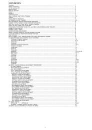
The contents of this service information:<br />
• The power supply circuit diagram that is<br />
divided into two separate parts:<br />
• 21” power supply circuit diagram<br />
- power supply circuit diagram for 25” and 28”<br />
• fault-finding tree for repairing the television<br />
because:<br />
- the error register in the service menu is not<br />
filled in sets bearing code QG00 for the<br />
Netherlands and Italy. For all other countries<br />
the error registers in the service menus of<br />
sets bearing code QG03 and lower is not<br />
filled.<br />
• Introduction of two new features, 16:9 module<br />
and WSSB (wide screen signalling bit<br />
detection) module, with accompanying copper<br />
track layout and spare parts list with accompanying<br />
diagram.<br />
Description of the new features in the <strong>MD</strong><strong>1.1</strong><br />
TV set.<br />
The WSSB enables the TV set to switch<br />
automatically to the various display formats<br />
(16:9 letterbox, 14:9 letterbox, 4:3) using<br />
signalling bits. The signalling bits are transmitted<br />
in line 23 of the video signal. IC7119<br />
(TDA8366) is used to match the convergence to<br />
the various formats in cooperation with the 16:9<br />
panel.<br />
Table 1<br />
ITEM DESCRIPTION SERVICE CODE<br />
NUMBER<br />
LARGE SIGNAL PANEL<br />
F1501 2183.15 (3.15A) 4822 070 33152<br />
C2420 1nF 10%2KV 4822 126 13449<br />
C2425 15nF 5%1.6KV 5322 121 44345<br />
C2426 12nF 5%1.6KV 4822 121 70618<br />
C2470 4.7nF 5% 250V 4822 121 43856<br />
C2479 330nF 5% 63V 5322 121 42661<br />
R3421 68KΩ 5% 0.5W 4822 116 52297<br />
R3470 1.5MΩ 5% 0.5W 4822 116 81783<br />
R3479 680KΩ 5% 0.5W 4822 116 52298<br />
R3480 120KΩ 5%0.5W 4822 116 52239<br />
R3482 680KΩ 5% 0.5W 4822 116 52298<br />
R3483 10Ω 5% 0.5W 4822 116 52176<br />
R3484 6.8RΩ 1% 0.6W 4822 050 26808<br />
R3506 18Ω-3KQ PTC/PTC 25% 4822 117 12027<br />
R3507 18Ω-3Kg PTC/PTC 25% 4822 117 12027<br />
R3625 100Ω LIN 4822 101 11319<br />
R3626 4.7Ω 1% 0.6W 4822 050 24708<br />
R3627 10Ω 5% 0.5W 4822 116 52176<br />
L5421 Lin. Corr. Coil LC90 4822 157 10992<br />
L5424 Bal. Coil 4822 157 10993<br />
L5463 10µH 4822 157 51462<br />
L5550 Transf. pow. 10300300-P1 4822 146 10705<br />
D6424 BYW96E 5322 130 32042<br />
D6482 BZX79-B68 4822 130 30864<br />
T7480 IRF520FI 4822 130 61706<br />
SMALL SIGNAL PANEL<br />
7600 µP MIWS1111 (3324) (F,D,NL,I,E) 4822 900 10853<br />
7600 µP MIWS1211 (S,DK,N,Fl,GB) 4822 900 10851<br />
7600 µP MIWS1311 (GB,E,P,GR) 4822 900 10852<br />
7600 µP MIWS1511 (3325) (GB,D,NL) 4822 900 10855<br />
7600 µP MIWS1611 (GB,HU,POL,CZ,RU) 4822 900 10854<br />
Audio Amp Diagram<br />
1. <strong>MD</strong><strong>1.1</strong> E 28” WideScreen<br />
The information published in the Service Manual<br />
and SI <strong>MD</strong>1 .1 -E 95.01 is also valid for <strong>MD</strong>1 .1<br />
E 28” WideScreen sets. However, there is some<br />
diversity in the spare parts list (See Table 1).<br />
2. Microprocessors<br />
The listed microprocessors (Table 1) can be<br />
used for “24” and “28” Widescreen <strong>MD</strong><strong>1.1</strong> E sets.<br />
When the µPs are used in a “28” WS set, the<br />
option “28” in the Service Alignment Menu<br />
should be set to “Y”. When the µPs are used in<br />
a 24” WS set, the option “28” should be set to<br />
“N”.“28 N” is the default value of these µPs after<br />
replacement.<br />
3. Mechanics<br />
The mechanical execution of the WideScreen<br />
sets (24” and 28”) differs from the other <strong>MD</strong>1 .1<br />
E sets. Service positions and other mechanical<br />
intructions are described in the <strong>MD</strong>1 .2E Service<br />
section (Styling with top control and side input/<br />
output).<br />
CRT PANEL<br />
C2300 220pF 50V 4822 122 31173<br />
R3304 47W 5% 4822 116 52195<br />
R3310 5K6Ω 5% 4822 116 52289<br />
R3312 6K8Ω 5% 4822 116 83961<br />
R3324 47Ω 5% 4822 116 52195<br />
R3344 47Ω 5% 4822 116 52195<br />
L5381 39uH 4822 157 70703<br />
Audio<br />
Module<br />
Interface<br />
Diagram<br />
CTI/Black Stretch Diagram<br />
4. Black Stretch Panel<br />
In a number of <strong>MD</strong>1 .1 E sets, a Black Stretch<br />
panel [F] is used. This panel increases the detail<br />
of dark parts of the picture. The schematic, layout<br />
and spare parts list of this panel are<br />
published in this SI.<br />
Electrical Adjustments / Safety Parts / Service Notes / Controls Diagram / CRT Diagram / Euroconnector 1 & 2 / Fault Finding Tree ...(16:9) / Front Control Diagram<br />
Horizontal Output Diagram / Audio Amp / Audio Module Interface / Audio Module / CTI/Black Stretch Diagram / Nicam Diagram / Power Supply Block / Tuner IF Diagram<br />
Power Supply Diagram / Power Supply Diagrams (21” 16:9) (25/28”/16:9) / 16:9 Module Diagram / Small Signal Panel / Sound IF Diagram / Text Diagram / Sync. Diagram<br />
Synchronisation Block / Testpoint Diagrams / Vertical Output Diagram / Video Processing / Video Processing Block / Waveforms / WSSB Module Diagram
<strong>PHILIPS</strong> <strong>MD</strong> <strong>1.1</strong> E (<strong>AA</strong>) <strong>Chassis</strong><br />
3<br />
Audio Module Diagram<br />
Electrical Adjustments / Safety Parts / Service Notes / Controls Diagram / CRT Diagram / Euroconnector 1 & 2 / Fault Finding Tree ...(16:9) / Front Control Diagram<br />
Horizontal Output Diagram / Audio Amp / Audio Module Interface / Audio Module / CTI/Black Stretch Diagram / Nicam Diagram / Power Supply Block / Tuner IF Diagram<br />
Power Supply Diagram / Power Supply Diagrams (21” 16:9) (25/28”/16:9) / 16:9 Module Diagram / Small Signal Panel / Sound IF Diagram / Text Diagram / Sync. Diagram<br />
Synchronisation Block / Testpoint Diagrams / Vertical Output Diagram / Video Processing / Video Processing Block / Waveforms / WSSB Module Diagram
<strong>PHILIPS</strong> <strong>MD</strong> <strong>1.1</strong> E (<strong>AA</strong>) <strong>Chassis</strong><br />
Nicam<br />
Diagram<br />
4<br />
Controls Diagram<br />
Sound IF<br />
Diagram<br />
Electrical Adjustments / Safety Parts / Service Notes / Controls Diagram / CRT Diagram / Euroconnector 1 & 2 / Fault Finding Tree ...(16:9) / Front Control Diagram<br />
Horizontal Output Diagram / Audio Amp / Audio Module Interface / Audio Module / CTI/Black Stretch Diagram / Nicam Diagram / Power Supply Block / Tuner IF Diagram<br />
Power Supply Diagram / Power Supply Diagrams (21” 16:9) (25/28”/16:9) / 16:9 Module Diagram / Small Signal Panel / Sound IF Diagram / Text Diagram / Sync. Diagram<br />
Synchronisation Block / Testpoint Diagrams / Vertical Output Diagram / Video Processing / Video Processing Block / Waveforms / WSSB Module Diagram
<strong>PHILIPS</strong> <strong>MD</strong> <strong>1.1</strong> E (<strong>AA</strong>) <strong>Chassis</strong><br />
5<br />
Text Diagram<br />
Electrical Adjustments / Safety Parts / Service Notes / Controls Diagram / CRT Diagram / Euroconnector 1 & 2 / Fault Finding Tree ...(16:9) / Front Control Diagram<br />
Horizontal Output Diagram / Audio Amp / Audio Module Interface / Audio Module / CTI/Black Stretch Diagram / Nicam Diagram / Power Supply Block / Tuner IF Diagram<br />
Power Supply Diagram / Power Supply Diagrams (21” 16:9) (25/28”/16:9) / 16:9 Module Diagram / Small Signal Panel / Sound IF Diagram / Text Diagram / Sync. Diagram<br />
Synchronisation Block / Testpoint Diagrams / Vertical Output Diagram / Video Processing / Video Processing Block / Waveforms / WSSB Module Diagram
<strong>PHILIPS</strong> <strong>MD</strong> <strong>1.1</strong> E (<strong>AA</strong>) <strong>Chassis</strong><br />
Power Supply Block Diagram<br />
6<br />
Testpoint Diagrams<br />
Power Supply<br />
Synchronisation<br />
Small Signal Panel<br />
Synchronisation Block Diagram<br />
Electrical Adjustments / Safety Parts / Service Notes / Controls Diagram / CRT Diagram / Euroconnector 1 & 2 / Fault Finding Tree ...(16:9) / Front Control Diagram<br />
Horizontal Output Diagram / Audio Amp / Audio Module Interface / Audio Module / CTI/Black Stretch Diagram / Nicam Diagram / Power Supply Block / Tuner IF Diagram<br />
Power Supply Diagram / Power Supply Diagrams (21” 16:9) (25/28”/16:9) / 16:9 Module Diagram / Small Signal Panel / Sound IF Diagram / Text Diagram / Sync. Diagram<br />
Synchronisation Block / Testpoint Diagrams / Vertical Output Diagram / Video Processing / Video Processing Block / Waveforms / WSSB Module Diagram
<strong>PHILIPS</strong> <strong>MD</strong> <strong>1.1</strong> E (<strong>AA</strong>) <strong>Chassis</strong><br />
7<br />
Video Processing Block Diagram<br />
Waveforms<br />
Power Supply<br />
Synchronisation<br />
Small Signal Panel<br />
Diagram<br />
Synchronisation Diagram<br />
Small Signal Panel<br />
Electrical Adjustments / Safety Parts / Service Notes / Controls Diagram / CRT Diagram / Euroconnector 1 & 2 / Fault Finding Tree ...(16:9) / Front Control Diagram<br />
Horizontal Output Diagram / Audio Amp / Audio Module Interface / Audio Module / CTI/Black Stretch Diagram / Nicam Diagram / Power Supply Block / Tuner IF Diagram<br />
Power Supply Diagram / Power Supply Diagrams (21” 16:9) (25/28”/16:9) / 16:9 Module Diagram / Small Signal Panel / Sound IF Diagram / Text Diagram / Sync. Diagram<br />
Synchronisation Block / Testpoint Diagrams / Vertical Output Diagram / Video Processing / Video Processing Block / Waveforms / WSSB Module Diagram
<strong>PHILIPS</strong> <strong>MD</strong> <strong>1.1</strong> E (<strong>AA</strong>) <strong>Chassis</strong><br />
8<br />
Video Processing Block Diagram<br />
Electrical Adjustments / Safety Parts / Service Notes / Controls Diagram / CRT Diagram / Euroconnector 1 & 2 / Fault Finding Tree ...(16:9) / Front Control Diagram<br />
Horizontal Output Diagram / Audio Amp / Audio Module Interface / Audio Module / CTI/Black Stretch Diagram / Nicam Diagram / Power Supply Block / Tuner IF Diagram<br />
Power Supply Diagram / Power Supply Diagrams (21” 16:9) (25/28”/16:9) / 16:9 Module Diagram / Small Signal Panel / Sound IF Diagram / Text Diagram / Sync. Diagram<br />
Synchronisation Block / Testpoint Diagrams / Vertical Output Diagram / Video Processing / Video Processing Block / Waveforms / WSSB Module Diagram
<strong>PHILIPS</strong> <strong>MD</strong> <strong>1.1</strong> E (<strong>AA</strong>) <strong>Chassis</strong><br />
9<br />
CRT Diagram<br />
Electrical Adjustments / Safety Parts / Service Notes / Controls Diagram / CRT Diagram / Euroconnector 1 & 2 / Fault Finding Tree ...(16:9) / Front Control Diagram<br />
Horizontal Output Diagram / Audio Amp / Audio Module Interface / Audio Module / CTI/Black Stretch Diagram / Nicam Diagram / Power Supply Block / Tuner IF Diagram<br />
Power Supply Diagram / Power Supply Diagrams (21” 16:9) (25/28”/16:9) / 16:9 Module Diagram / Small Signal Panel / Sound IF Diagram / Text Diagram / Sync. Diagram<br />
Synchronisation Block / Testpoint Diagrams / Vertical Output Diagram / Video Processing / Video Processing Block / Waveforms / WSSB Module Diagram
<strong>PHILIPS</strong> <strong>MD</strong> <strong>1.1</strong> E (<strong>AA</strong>) <strong>Chassis</strong><br />
10<br />
Euroconnector 1 Diagram<br />
Euroconnector 2 Diagram<br />
Electrical Adjustments / Safety Parts / Service Notes / Controls Diagram / CRT Diagram / Euroconnector 1 & 2 / Fault Finding Tree ...(16:9) / Front Control Diagram<br />
Horizontal Output Diagram / Audio Amp / Audio Module Interface / Audio Module / CTI/Black Stretch Diagram / Nicam Diagram / Power Supply Block / Tuner IF Diagram<br />
Power Supply Diagram / Power Supply Diagrams (21” 16:9) (25/28”/16:9) / 16:9 Module Diagram / Small Signal Panel / Sound IF Diagram / Text Diagram / Sync. Diagram<br />
Synchronisation Block / Testpoint Diagrams / Vertical Output Diagram / Video Processing / Video Processing Block / Waveforms / WSSB Module Diagram
<strong>PHILIPS</strong> <strong>MD</strong> <strong>1.1</strong> E (<strong>AA</strong>) <strong>Chassis</strong><br />
11<br />
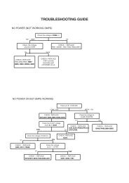
Fault Finding Tree Fault Finding Tree (16:9)<br />
Electrical Adjustments / Safety Parts / Service Notes / Controls Diagram / CRT Diagram / Euroconnector 1 & 2 / Fault Finding Tree ...(16:9) / Front Control Diagram<br />
Horizontal Output Diagram / Audio Amp / Audio Module Interface / Audio Module / CTI/Black Stretch Diagram / Nicam Diagram / Power Supply Block / Tuner IF Diagram<br />
Power Supply Diagram / Power Supply Diagrams (21” 16:9) (25/28”/16:9) / 16:9 Module Diagram / Small Signal Panel / Sound IF Diagram / Text Diagram / Sync. Diagram<br />
Synchronisation Block / Testpoint Diagrams / Vertical Output Diagram / Video Processing / Video Processing Block / Waveforms / WSSB Module Diagram
<strong>PHILIPS</strong> <strong>MD</strong> <strong>1.1</strong> E (<strong>AA</strong>) <strong>Chassis</strong><br />
Front Control Diagram<br />
12<br />
Horizontal Output Diagram<br />
Electrical Adjustments / Safety Parts / Service Notes / Controls Diagram / CRT Diagram / Euroconnector 1 & 2 / Fault Finding Tree ...(16:9) / Front Control Diagram<br />
Horizontal Output Diagram / Audio Amp / Audio Module Interface / Audio Module / CTI/Black Stretch Diagram / Nicam Diagram / Power Supply Block / Tuner IF Diagram<br />
Power Supply Diagram / Power Supply Diagrams (21” 16:9) (25/28”/16:9) / 16:9 Module Diagram / Small Signal Panel / Sound IF Diagram / Text Diagram / Sync. Diagram<br />
Synchronisation Block / Testpoint Diagrams / Vertical Output Diagram / Video Processing / Video Processing Block / Waveforms / WSSB Module Diagram
<strong>PHILIPS</strong> <strong>MD</strong> <strong>1.1</strong> E (<strong>AA</strong>) <strong>Chassis</strong><br />
13<br />
Power Supply Diagram<br />
Electrical Adjustments / Safety Parts / Service Notes / Controls Diagram / CRT Diagram / Euroconnector 1 & 2 / Fault Finding Tree ...(16:9) / Front Control Diagram<br />
Horizontal Output Diagram / Audio Amp / Audio Module Interface / Audio Module / CTI/Black Stretch Diagram / Nicam Diagram / Power Supply Block / Tuner IF Diagram<br />
Power Supply Diagram / Power Supply Diagrams (21” 16:9) (25/28”/16:9) / 16:9 Module Diagram / Small Signal Panel / Sound IF Diagram / Text Diagram / Sync. Diagram<br />
Synchronisation Block / Testpoint Diagrams / Vertical Output Diagram / Video Processing / Video Processing Block / Waveforms / WSSB Module Diagram
<strong>PHILIPS</strong> <strong>MD</strong> <strong>1.1</strong> E (<strong>AA</strong>) <strong>Chassis</strong><br />
Power Supply (21” 16:9) Diagram<br />
14<br />
Power Supply (25” & 28” 16:9) Diagram<br />
Electrical Adjustments / Safety Parts / Service Notes / Controls Diagram / CRT Diagram / Euroconnector 1 & 2 / Fault Finding Tree ...(16:9) / Front Control Diagram<br />
Horizontal Output Diagram / Audio Amp / Audio Module Interface / Audio Module / CTI/Black Stretch Diagram / Nicam Diagram / Power Supply Block / Tuner IF Diagram<br />
Power Supply Diagram / Power Supply Diagrams (21” 16:9) (25/28”/16:9) / 16:9 Module Diagram / Small Signal Panel / Sound IF Diagram / Text Diagram / Sync. Diagram<br />
Synchronisation Block / Testpoint Diagrams / Vertical Output Diagram / Video Processing / Video Processing Block / Waveforms / WSSB Module Diagram
<strong>PHILIPS</strong> <strong>MD</strong> <strong>1.1</strong> E (<strong>AA</strong>) <strong>Chassis</strong><br />
Tuner IF Diagram<br />
15<br />
16:9 Module Diagram<br />
Vertical Output Diagram<br />
WSSB Module Diagram<br />
Electrical Adjustments / Safety Parts / Service Notes / Controls Diagram / CRT Diagram / Euroconnector 1 & 2 / Fault Finding Tree ...(16:9) / Front Control Diagram<br />
Horizontal Output Diagram / Audio Amp / Audio Module Interface / Audio Module / CTI/Black Stretch Diagram / Nicam Diagram / Power Supply Block / Tuner IF Diagram<br />
Power Supply Diagram / Power Supply Diagrams (21” 16:9) (25/28”/16:9) / 16:9 Module Diagram / Small Signal Panel / Sound IF Diagram / Text Diagram / Sync. Diagram<br />
Synchronisation Block / Testpoint Diagrams / Vertical Output Diagram / Video Processing / Video Processing Block / Waveforms / WSSB Module Diagram
<strong>PHILIPS</strong> <strong>MD</strong> <strong>1.1</strong> E (<strong>AA</strong>) <strong>Chassis</strong><br />
16<br />
Video Processing Diagram<br />
Electrical Adjustments / Safety Parts / Service Notes / Controls Diagram / CRT Diagram / Euroconnector 1 & 2 / Fault Finding Tree ...(16:9) / Front Control Diagram<br />
Horizontal Output Diagram / Audio Amp / Audio Module Interface / Audio Module / CTI/Black Stretch Diagram / Nicam Diagram / Power Supply Block / Tuner IF Diagram<br />
Power Supply Diagram / Power Supply Diagrams (21” 16:9) (25/28”/16:9) / 16:9 Module Diagram / Small Signal Panel / Sound IF Diagram / Text Diagram / Sync. Diagram<br />
Synchronisation Block / Testpoint Diagrams / Vertical Output Diagram / Video Processing / Video Processing Block / Waveforms / WSSB Module Diagram