
You also want an ePaper? Increase the reach of your titles
YUMPU automatically turns print PDFs into web optimized ePapers that Google loves.
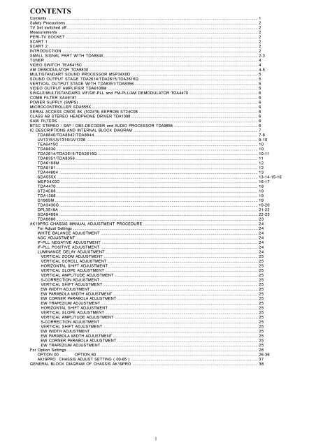
<strong>CONTENTS</strong><br />
Contents ................................................................................................................................................................................................. 1<br />
Safety Precautions ................................................................................................................................................................................ 2<br />
TV Set switched off ............................................................................................................................................................................... 2<br />
Measurements ....................................................................................................................................................................................... 2<br />
PERI-TV SOCKET ................................................................................................................................................................................ 2<br />
SCART 1 ................................................................................................................................................................................................ 2<br />
SCART 2 ................................................................................................................................................................................................ 2<br />
INTRODUCTION ................................................................................................................................................................................... 2<br />
SMALL SIGNAL PART WITH TDA884X ............................................................................................................................................. 2-3<br />
TUNER ................................................................................................................................................................................................... 4<br />
VIDEO SWITCH TEA6415C ................................................................................................................................................................ 4<br />
AM DEMODULATOR TDA9830 ........................................................................................................................................................... 4-5<br />
MULTISTANDART SOUND PROCESSOR MSP34X0D .................................................................................................................... 5<br />
SOUND OUTPUT STAGE TDA2614/TDA2615/TDA2616Q ............................................................................................................ 5<br />
VERTICAL OUTPUT STAGE WITH TDA8351/TDA8356 ................................................................................................................. 5<br />
VIDEO OUTPUT AMPLIFIER TDA6108M .......................................................................................................................................... 5<br />
SINGLE/MULTISTANDARD VIF/SIF-PLL and FM-PLL/AM DEMODULATOR TDA4470 ............................................................... 6<br />
COMB FILTER SAA9181 ..................................................................................................................................................................... 6<br />
POWER SUPPLY (SMPS) .................................................................................................................................................................... 6<br />
MICROCONTROLLER SDA555X ........................................................................................................................................................ 6<br />
SERIAL ACCESS CMOS 8K (1024*8) EEPROM ST24C08 ............................................................................................................. 6<br />
CLASS AB STEREO HEADPHONE DRIVER TDA1308 .................................................................................................................... 6<br />
SAW FILTERS ....................................................................................................................................................................................... 6<br />
BTSC STEREO / SAP / DBX-DECODER end AUDIO PROCESSOR TDA9855 ............................................................................. 6<br />
IC DESCRIPTIONS AND INTERNAL BLOCK DIAGRAM .................................................................................................................. 7<br />
TDA8840/TDA8842/TDA8844...................................................................................................................................................... 7-8<br />
UV1315/UV1316/UV1336 ............................................................................................................................................................. 9-10<br />
TEA6415C ...................................................................................................................................................................................... 10<br />
TDA9830......................................................................................................................................................................................... 10<br />
TDA2614/TDA2615/TDA2616Q................................................................................................................................................... 10-11<br />
TDA8351/TDA8356 ....................................................................................................................................................................... 11<br />
TDA6108M ..................................................................................................................................................................................... 12<br />
TDA9181......................................................................................................................................................................................... 12<br />
TDA44604 ...................................................................................................................................................................................... 13<br />
SDA555X ........................................................................................................................................................................................ 13-14-15-16<br />
MSP34X0D ..................................................................................................................................................................................... 16-17<br />
TDA4470......................................................................................................................................................................................... 18<br />
ST24C08......................................................................................................................................................................................... 19<br />
TDA1308......................................................................................................................................................................................... 19<br />
G1965M .......................................................................................................................................................................................... 19<br />
TDA3430G ...................................................................................................................................................................................... 19-20<br />
DPL3519A ...................................................................................................................................................................................... 21-22<br />
SDA9488A ...................................................................................................................................................................................... 22-23<br />
TDA9886......................................................................................................................................................................................... 23<br />
AK19PRO CHASSIS MANUAL ADJUSTMENT PROCEDURE ......................................................................................................... 24<br />
For Adjust Settings ......................................................................................................................................................................... 24<br />
WHITE BALANCE ADJUSTMENT ................................................................................................................................................ 24<br />
AGC ADJUSTMENT ....................................................................................................................................................................... 24<br />
IF-PLL NEGATIVE ADJUSTMENT ............................................................................................................................................... 24<br />
IF-PLL POSITIVE ADJUSTMENT ................................................................................................................................................ 24<br />
LUMINANCE DELAY ADJUSTMENT ............................................................................................................................................ 24<br />
VERTICAL ZOOM ADJUSTMENT ............................................................................................................................................. 25<br />
VERTICAL SCROLL ADJUSTMENT .......................................................................................................................................... 25<br />
HORIZONTAL SHIFT ADJUSTMENT ......................................................................................................................................... 25<br />
VERTICAL SLOPE ADJUSTMENT ............................................................................................................................................ 25<br />
VERTICAL AMPLITUDE ADJUSTMENT ................................................................................................................................... 25<br />
S-CORRECTION ADJUSTMENT ................................................................................................................................................ 25<br />
VERTICAL SHIFT ADJUSTMENT .............................................................................................................................................. 25<br />
EW WIDTH ADJUSTMENT .......................................................................................................................................................... 25<br />
EW PARABOLA WIDTH ADJUSTMENT ..................................................................................................................................... 25<br />
EW CORNER PARABOLA ADJUSTMENT ................................................................................................................................. 25<br />
EW TRAPEZIUM ADJUSTMENT ................................................................................................................................................ 25<br />
For Option Settings ............................................................................................................................................................................... 26<br />
OPTION 00 ...... OPTION 60 .................................................................................................................................................... 26-36<br />
AK19PRO CHASSIS ADJUST SETTING ( 00-65 ) .................................................................................................................... 37<br />
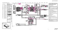
GENERAL BLOCK DIAGRAM OF CHASSIS AK19PRO ................................................................................................................... 38<br />
1
DO NOT CHANGE ANY MODULE UNLESS THE SET IS SWITCH OFF<br />
The mains supply side of the switch mode power supply transformer is live.<br />
Use an isolating transformer.<br />
The receivers fulfill completely the safety requirements.<br />
Safety precautions:<br />
Servicing of this TV should only be carried out by a qualified person.<br />
- Components marked with the warning symbol on the circuit diagram are critical for safety and must only be replaced with an identical<br />
component.<br />
- Power resistor and fusable resistors must be mounted in an identical manner to the original component.<br />
- When servicing this TV, check that the EHT does not exceed 26kV.<br />
TV Set switched off:<br />
Make short-circuit between HV-CRT clip and CRT ground layer.<br />
Short C804 (150mF) before changing IC802 or other components in primary side of SMPS.<br />
Measurements:<br />
Voltage readings and oscilloscope traces are measured under following conditions.<br />
Antenna signal 60dB from colourbar generator. (100% white, 75% colour saturation)<br />
Brightness, contrast, colour set for a normal picture.<br />
Mains supply, 220VAC, 50Hz.<br />
PERI-TV SOCKET<br />
SCART 1 (SC050)<br />
SCART 2 (SC051)<br />
1 Audio right output 0.5Vrms / 1K 1 Audio right output 0.5Vrms / 1K<br />
2 Audio right input 0.5Vrms / 10K 2 Audio right input 0.5Vrms / 10K<br />
3 Audio left output 0.5Vrms / 1K 3 Audio left output 0.5Vrms / 1K<br />
4 Ground AF 4 Ground AF<br />
5 Ground Blue 5 Ground Blue<br />
6 Audio left input 0.5Vrms / 10K 6 Audio left input 0.5Vrms / 10K<br />
7 Blue input 0.7Vpp / 75ohm 7 Blue input 0.7Vpp / 75ohm<br />
8 AV switching input 0-12VDC /10K 8 AV switching input 0-12VDC /10K<br />
9 Ground Green 9 Ground Green<br />
10 - 10 -<br />
11 Green input 0.7Vpp / 75ohm 11 -<br />
12 - 12 -<br />
13 Ground Red 13 Ground Red<br />
14 Ground Blanking 14 Ground Blanking<br />
15 Red input 0.7Vpp / 75ohm 15 -<br />
16 Blanking input 0-0.4VDC, 1-3VDC / 75ohm 16 -<br />
17 Ground CVS output 17 Ground CVS output<br />
18 Ground CVS input 18 Ground CVS input<br />
19 CVS output 1Vpp / 75ohm 19 CVS output 1Vpp / 75ohm<br />
20 CVS input 1Vpp / 75ohm 20 CVS input 1Vpp / 75ohm<br />
21 Ground 21 Ground<br />
1. INTRODUCTION<br />
11AK19 is a 90ø and 110ø chassis capable of driving 20-21”,24”,25”,28-29”,32”,33” tubes at appropriate currents.<br />
The chassis is capable of working in both PAL and SECAM. The sound system is capable of giving 6watts<br />
RMS output into a load of 8ohms.<br />
One 8 page simple TELETEXT, TOPTEXT and FASTEXT is provided.<br />
The chassis is equipped with 21-pin scart connectors which can accept via scart the SVHS format from VCRs so equipped.<br />
2. SMALL SIGNAL PART WITH TDA884X<br />
The TDA8840/8842/8844 combine all small signal functions required for a colour TV receiver, except tuning.<br />
2.1. Vision IF amplifier<br />
The IF-amplifier contains 3 AC-coupled control stages with a total gain control range which is higher than 66dB.<br />
The sensitivity of the circuit is comparable with that of modern IF-IC’ s. The video signal is demodulated by means of a PLL<br />
carrier regenerator. This circuit contains a frequency detector and a phase detector. The AFC output is obtained by using the<br />
VCO control voltage of the PLL and can be read via the I²C-bus. For fast search tuning systems the window of<br />
the AFC can be increased with a factor 3. The setting is realised with the AFW bit.<br />
Depending on the type the AGC-detector operates on top-sync level (single standard versions) or on top sync and top<br />
white-level (multi standard versions). The demodulation polarity is switched via the I²C-bus. The AGC detector time-constant<br />
capacitor is connected externally. This mainly because of the flexibility of the application. The time-constant of the AGC<br />
system during positive modulation is rather long to avoid visible variations of the signal amplitude.<br />
2
To improve the speed of the AGC system a circuit has been included which detects whether the AGC detector is activated every frame<br />
period. When during 3 frame periods no action is detected the speed of the system is increased. For signals without peak white<br />
information the system switches automatically to a gated black level AGC. Because a black level clamp pulse is required for this way<br />
of operation the circuit will only switch to black level AGC in the internal mode.<br />
The circuits contain a video identification circuit which is independent of the synchronisation circuit. Therefore search tuning is<br />
possible when the display section of the receiver is used as a monitor. The ident output is supplied to the tuning system via<br />
the I²C-bus. The video ident circuit can be made less sensitive by means of the STM bit. This mode can be used during search<br />
tuning to avoid that the tuning system will stop at very weak input signals.<br />
2.2. Video Switches<br />
The circuits have two CVBS inputs (internal and external CVBS) and Y/C input. When the Y/C input is not required the Y input can be<br />
used as third CVBS input. The selection of the various sources is made via the I²C-bus. The circuit has one CVBS output.<br />
2.3. Sound Circuit<br />
The sound band pass and trap filters have to be connected externally. The filtered intercarrier signal is fed to a limiter circuit<br />
and is demodulated by means of a PLL demodulator. This PLL circuit tunes itself automatically to the incoming carrier signal<br />
so that no adjustment is required.<br />
The volume is controlled via the I²C-bus. The deemphasis capacitor has to be connected externally. The non-controlled audio<br />
signal can be obtained from this pin. The FM demodulator can be muted via the I²C-bus. This function can be used to switch-off<br />
the sound during a channel change so that high output peaks are prevented. The TDA8840/8842 contain an automatic volume<br />
levelling (AVL) circuit which automatically stabilises the audio output signal to a certain level which can be set by the viewer by means<br />
of the volume control. This function prevents big audio output fluctuations due to variations of the modulation depth of the transmitter.<br />
The AVL function can be activated via the I²C-bus.<br />
2.4. Synchronisation circuit<br />
The sync seperator is preceded by a controlled amplifier which adjusts the sync pulse amplitude to a fixed level. These pulses<br />
are fed to the slicing stage which is operating at 50% of the amplitude. The separated sync pulses are fed to the first phase<br />
detector and to the coincidence detector. This coincidence detector is used to detect whether the line oscillator is synchronised<br />
and can also be used for transmitter identification. The first PLL has a very high statical steepness so that the phase of the<br />
picture is independent of the line frequency. The horizontal output signal is generated by means of an oscillator which is running at<br />
twice the line frequency. Its frequency is divided by 2 to lock the first control loop to the incoming signal. The time-constant of the loop<br />
can be forced by the I²C-bus (fast or slow).<br />
If required the IC can select the time-constant depending on the noise content of the incoming video signal.<br />
To protect the horizontal output transistor, the horizontal drive is immediately switched off when a power-on-reset is detected .<br />
The drive signal is switched-on again when the normal switch-on procedure is followed.<br />
Via the I²C-bus, adjustments can be made of the horizontal and vertical geometry. The vertical sawtooth generator drives the<br />
vertical output drive circuit which has a differrential output current. For the EW drive a single ended current output is available.<br />
When the horizontal scan is reduced to display 4 : 3 pictures on a 16 : 9 picture tube an accurate video blanking can be switched on<br />
to obtain well defined edges on the screen.<br />
Overvoltage conditions can be detected via the EHT tracking pin.When an overvoltage condition is detected the horizontal output<br />
drive signal will be switched-off via the slow stop procedure but it is also possible that the drive is not switched-off and that just a<br />
protection indication is given in the I²C-bus output byte. The choice is made via the input bit PRD.<br />
2.5. Chroma and Luminance processing<br />
The circuits contain a chroma bandpass and trap circuit. The filters are realised by means of gyrator circuits and they are<br />
automatically calibrated by comparing the tuning frequency with the X-tal frequency of the decoder.<br />
The luminance delay line and the delay for the peaking circuit are also realised by means of gyrator circuits.<br />
The centre frequency of the chroma bandpass filter is switchable via the I²C-bus so that the performance can be optimised for<br />
“front-end” signals and external CVBS signals.<br />
During SECAM reception the centre frequency of the chroma trap is reduced to get a better suppression of the SECAM<br />
carrier frequencies.<br />
2.6. Colour Decoder<br />
The decoder contains an alignment-free X-tal oscillator, a killer circuit and two colour difference demodulators. The 90° phase shift<br />
for the reference signal is made internally.<br />
The IC contains an automatic colour limiting (ACL) circuit which prevents that oversaturation occurs when signals with a high<br />
chroma-to-burst ratio are received. The ACL circuit is designed such that it only reduces the chroma signal and not the burst signal.<br />
This has the advantage that the colour sensitivity is not affected by this function.<br />
The base-band delay line is integrated in the PAL/SECAM IC’ s.<br />
The demodulated colour difference signals are internally supplied to the delay line. The matrixed signals are externally available.<br />
The colour difference matrix switches automatically between<br />
PAL/SECAM and NTSC, however, it is also possible to fix the matrix in the PAL standard.<br />
Which colour standard the IC can decode depends on the external X-tals. The X-tal to be connected to pin 34 must have a frequency<br />
of 3.5 MHz (NTSC-M, PAL-M or PAL-N) and pin 35 can handle X-tals with a frequency of 4.4 and 3.5 MHz. To prevent calibration<br />
problems of the horizontal oscillator the external switching between the 2 X-tals should be carried out when the oscillator is forced to<br />
pin 35. For a reliable calibration of the horizontal oscillator it is very important that the X-tal indication bits (XA and XB) are not<br />
corrupted. For this reason the X-tal bits can be read in the output bytes so that the software can check the I²C-bus transmission.<br />
2.7. RGB output circuit and black-current stabilisation<br />
The colour-difference signals are matrixed with the luminance signal to obtain the RGB-signals. The TDA 884X device has one<br />
linear RGB input. This RGB signal can be controlled on contrast and brightness.<br />
The output signal has an amplitude of about 2 volts black-to-white at nominal input signals and nominal settings of the controls.<br />
To increase the flexibility of the IC it is possible to insert OSD and/or teletext signals directly at the RGB outputs.<br />
This insertion mode is controlled via the insertion input (pin 26 in the S-DIP 56- and pin 38 in the QFP-64 level). This blanking action<br />
at the RGB outputs has some delay which must be compansated externally.<br />
To obtain an accurate biasing of the picture tube a “Continuous Cathode Calibration” circuit has been developed.<br />
This function is realised by means of a 2-point black level stabilisation circuit.<br />
When the TV receiver is switched-on, the RGB output signals are blanked and the black current loop will try to set the right picture<br />
tube bias levels.Via the AST bit a choice can be made between automatic start-up or a start-up via the m-processor.<br />
3
3. TUNER<br />
Either a PLL or a VST tuner is used as a tuner.<br />
UV1316 (VHF/UHF) is used as a PLL tuner. For only PALM/N, NTSC M applications UV 1336 is used as the PLL tuner. UV 1315 (VHF/<br />
UHF) is used as a VST Tuner.<br />
Channel coverage of UV1316:<br />
BAND<br />
OFF-AIR CHANNELS<br />
CABLE CHANNELS<br />
CHANNELS FREQUENCY CHANNELS FREQUENCY<br />
RANGE (MHz)<br />
RANGE (MHz)<br />
Low Band E2 to C 48.25 to 82.25 (1) S01 to S08 69.25 to 154.25<br />
Mid Band E5 to E12 175.25 to 224.25 S09 to S38 161.25 to 439.25<br />
High Band E21 to E69 471.25 to 855.25 (2) S39 to S41 447.25 to 463.25<br />
(1). Enough margin is available to tune down to 45.25 MHz.<br />
(2). Enough margin is available to tune up to 863.25 MHz.<br />
Noise Typical Max. Gain Min. Typical Max.<br />
Low band : 5dB 9dB All channels : 38dB 44dB 52dB<br />
Mid band : 5dB 9dB Gain Taper (of-air channels) : - - 8dB<br />
High band : 6dB 9dB<br />
Channel Coverage UV1336:<br />
BAND CHANNELS FREQUENCY<br />
RANGE (MHz)<br />
Low Band 2 to D 55.25 to 139.25<br />
Mid Band E to PP 145.25 to 391.25<br />
High Band QQ to 69 397.25 to 801.25<br />
Noise is typically 6dB for all channels. Gain is minimum 38dB and maximum 50dB for all channels.<br />
Channel Coverage of UV1315:<br />
BAND<br />
OFF-AIR CHANNELS CABLE CHANNELS<br />
CHANNELS FREQUENCY CHANNELS FREQUENCY<br />
RANGE (MHz)<br />
RANGE (MHz)<br />
Low Band E2 to C 48.25 to 82.25 (1) S01 to S10 69.25 to 168.25<br />
Mid Band E5 to E12 175.25 to 224.25 S11 to S39 231.25 to 447.25<br />
High Band E21 to E69 471.25 to 855.25 (2) S40 to S41 455.25 to 463.25<br />
(1). Enough margin is available to tune down to 45.25 MHz.<br />
(2). Enough margin is available to tune up to 863.25 MHz.<br />
Noise Typ. Max. Gain Min. Typ. Max.<br />
Low band : 6dB 9dB All Channels 38dB 44dB 50dB<br />
Mid band : 6dB 10dB Gain Taper - - 8dB<br />
High band : 6dB 11dB (off-air channels)<br />
4.VIDEO SWITCH TEA6415C<br />
In case of three or more external sources are used, the video switch IC TEA6415C is used. The main function of this device is to switch<br />
8 video input sources on the 6 outputs.<br />
Each output can be switched on only one of each input. On each input an alignment of the lowest level of the signal is made (bottom<br />
of sync. top for CVBS or black level for RGB signals).<br />
Each nominal gain between any input and output is 6.5dB.For D2MAC or Chroma signal the alignment is switched off by forcing, with<br />
an external resistor bridge, 5VDC on the input. Each input can be used as a normal input or as a MAC or Chroma input (with external<br />
resistor bridge). All the switching possibilities are changed through the BUS.<br />
Driving 75ohm load needs an external resistor.<br />
It is possible to have the same input connected to several outputs.<br />
4
5. AM DEMODULATOR TDA9830<br />
The TDA9830 is designed for AM-sound demodulation used in L and L’ standard.<br />
Sound IF Input:<br />
The sound IF amplifier consists of three AC-coupled differential amplifier stages each with approximately 20dB gain.<br />
At the output of each stage is a multiplier for gain controlling. The overall control range is approximately -6 to +60dB and the<br />
frequency response (-3dB) of the IF amplifier is approximately 6 to 70MHz. The steepness of gain control is approximately 10mV/dB.<br />
IF AGC:<br />
The automatic gain control voltage to maintain the AM demodulator output signal at a constant level is generated by a mean<br />
level detector.The AGC-detector charges and discharges the capacitor at pin 3 controlled by the output signal of the<br />
AM-demodulator compared to an internal reference voltage.The maximum charge/discharge current is approximately 5 mA.<br />
AM-demodulator<br />
The IF amplifier output signal is fed to a limiting amplifier (two stages) and to a multiplier circuit.<br />
However the limiter output signal (which is not any more AM modulated) is also fed to the multiplier, which provides AM<br />
demodulation (in phase demodulation). After lowpass filtering (fg @ 400kHz) for carrier rejection and buffering,<br />
the demodulator output signal is present at pin 6.<br />
Audio Switch<br />
This circuit is an operational amplifier with three input stages and internal feedback network determining gain (0dB) and<br />
frequency response (fg @ 700kHz). Two of the input stages are connected to pin 7 and pin 9, the third input stage to an<br />
internal reference voltage. Controlled by the switching pins 10 and 12, one of the three input stages can be activated and a<br />
choice made between two different AF signals or mute state. The selected signal is present at pin 8. The decoupling capacitors<br />
at the input pins are needed, because the internally generated bias voltage for the input stages must not be influenced<br />
by the application in order to avoid DC-plop in case of switching.<br />
Reference Circuit:<br />
This circuit is a band gap stabiliser in combination with a voltage regulation amplifier, which provides an internal reference voltage<br />
of about 3.6V nearly independent from supply voltage and temperature. This reference voltage is filtered by the capacitor at<br />
pin 4 in order to reduce noise. It is used as a reference to generate all important voltages and currents of the circuit.<br />
For application in 12V power supply concepts, there is an internal voltage divider in combination with a Darlington transistor in<br />
order to reduce the supply voltage for all IC function blocks to approximately 6V.<br />
6. MULTISTANDARD SOUND PROCESSOR:<br />
The MSP 34x0D is designed to perform demodulation of FM or AM-Mono TV sound. Alternatively, two-carrier FM systems<br />
according to the German or Korean terrestrial specs or the satellite specs can be processed with the MSP 34x0D.<br />
Digital demodulation and decoding of NICAM-coded TV stereo sound, is done only by the MSP 3410. The MSP 34x0D offers<br />
a powerful feature to calculate the carrier field strength which can be used for automatic standard detection (terrestrial) and<br />
search algorithms (satellite).<br />
7. SOUND OUTPUT STAGE TDA2614/TDA2615/TDA2616Q<br />
TDA2614 is used as the AF output amplifier for mono applications. It is supplied by ±12VDC coming from a separate winding in the<br />
SMPS transformer. An output power of 2*6W (THD=0.5%) can be delivered into an 8ohm load.<br />
TDA2615 is used as the AF output amplifier for stereo applications. It is supplied by<br />
±12VDC coming from a separate winding in the SMPS transformer. An output power of 2*6W (THD=0.5%)<br />
can be delivered into an 8ohm load.<br />
TDA2616Q is used as the AF output amplifier for stereo and dolby prologic applications. It is supplied by ±16VDC coming from<br />
a separate winding in the SMPS transformer. An output power of 2*12W (THD=0.5%) can be delivered into an 8ohm load.<br />
8. VERTICAL OUTPUT STAGE WITH TDA8351/8356<br />
The TDA8351/8356 vertical deflection circuit can be used in 90° and 110° deflection systems with field frequencies from<br />
50 up to 120Hz. With its bridge configuration the deflection output can be DC coupled with few external components.<br />
Only a single supply voltage for the scan and a second supply for the flyback are needed. The TDA8356 is intended for 90°<br />
systems and the TDA8351 is intended for 110° systems.<br />
The drive voltage is amplified by an amplifier and fed to two amplifiers, one is inverting and the other is a non inverting amplifier.<br />
The outputs (pins 7 and 4) are connected to the series connection of the vertical deflection coil and feedback resistor Rsense<br />
(R702//R703). The voltage across Rsense is fed via pin 9 to correction amplifier, to obtain a deflection current which is proportional<br />
to the drive voltage. The supply voltage for the TDA8351/8356 is 15VDC at pin 3. The supply voltage generator has a separate<br />
supply voltage of 45VDC at pin 6.<br />
9. VIDEO OUTPUT AMPLIFIER TDA6108M<br />
The TDA6108M consists of three monolithic video output amplifiers. The amplifier can be seen as an operational amplifier<br />
with negative feedback.<br />
The advantage of negative feedback is that the amplifier characteristics do not play an important role up to certain frequencies.<br />
The internal flash diodes protect the amplifiers against flash over in the picture tube.<br />
The only protections required at the cathode outputs are a flash resistor and a sparkgap.<br />
The TDA6108M has an internal thermal protection circuit which gives a decrease of the slew rate at high temperatures.<br />
Furthermore, the device needs only one power supply voltage (Vdd).<br />
In contrast to previous types of DMOS video amplifiers, all the external resistors (Rf, Ri and Ra) are integrated, so the gain is fixed<br />
and saves 9 resistors.<br />
Furthermore, the reference voltage is integrated, it saves a resistor divider and a decoupling capacitor. So, the replacement<br />
value of the TDA6108MQ is very high.<br />
The TDA6108M is provided with a black current data pin. Since TDA884X is used as drive device, no adjustments are required<br />
for gain and black setting, as the TDA884X has I²C white point adjustment and black current set-up.<br />
5
10. SINGLE/MULTISTANDARD VIF/SIF-PLL and FM-PLL/AM DEMODULATOR TDA4470<br />
The TDA4470 is an integrated bipolar circuit for multi-standard video / sound IF (VIF/SIF) signal processing, in TV/VCR and<br />
multimedia applications. The circuit processes all TV video IF signals with negative modulation (e.g.. B/G standard) posidive<br />
modulation (e.g.. L standard) and the AM, FM/NICAM sound IF signals.<br />
11. COMBFILTER TDA9181<br />
The TDA TDA 9181 is an adaptive PAL/NTSC comb filter with two internal delay lines, filters, clock control, and input clamps.<br />
Video standards PAL B, G, H, I, M and N NTSC M are supported. Two CVBS input signals can be selected by means of input switch.<br />
In addition to the comb filter the circuit contains an output switch so that a selection can be made between the combed CVBS<br />
signal and an external Y/C signal. The supply voltage is 5V.<br />
12. POWER SUPPLY (SMPS)<br />
The DC voltages required at various parts of the chassis are provided by an SMPS transformer controlled by the IC MC44604<br />
which is designed for driving, controlling and protecting switching transistor of SMPS. The transformer produces 150/115V for<br />
FBT input, ±14V for audio output IC, S+2.5V and S+3.3V for microcontroller, +15V for vertical output (field scan) and +33V for<br />
tuner and some other ICs and transistors.<br />
13. MICROCONTROLLER SDA5555<br />
The device is TV PRO tuning and control system based on the SDA 5555 TV TEXT microcontroller. It is designed for a low<br />
cost mono TV-SET with analogue picture and sound control. Neverthless the system offers an on screen display (OSD) and<br />
IR remote control of all functions.<br />
SDA5555 has the following features:<br />
- Display of program number, channel number, TV standard, analogue values, sleep timer, parental control, and mute is<br />
done by OSD.<br />
- Single LED for IR active, standby and on mode indication.<br />
- 1 Control line to select external source.<br />
- 3 Control lines for TV standard selection.<br />
- Frequency synthesis tuning (62.5 kHz steps)<br />
- 192 step fine tuning<br />
- Channels corresponding to standards B/G, OIRT, L and I (I+)<br />
- Mono sound control by analogue voltage<br />
- System configuration with service mode<br />
14. SERIAL ACCESS CMOS 8K (1024*8) EEPROM ST24C08<br />
The ST24C08 is a 8Kbit electrically erasable programmable memory (EEPROM), organised as 4 blocks of 256*8 bits.<br />
The memory is compatible with the I²C standard, two wire serial interface which uses a bi-directional data bus and serial clock.<br />
The memory carries a built-in 4 bit, unique device identification code (1010) corresponding to the I²C bus definition.<br />
This is used together with 1 chip enable input (E) so that up to 2*8K devices may be attached to the I²C bus and selected individually.<br />
15. CLASS AB STEREO HEADPHONE DRIVER TDA1308<br />
The TDA1308 is an integrated class AB stereo headphone driver contained in a DIP8 plastic package.<br />
The device is fabricated in a 1 mm CMOS process and has been primarily developed for portable digital audio applications.<br />
16. SAW FILTERS<br />
Saw filter type : Model:<br />
G1965M : PAL-SECAM B/G MONO<br />
G3962M : PAL-SECAM B/G GER&NIC STEREO, PAL I’ NIC STEREO, INT-1<br />
G1984 : PAL-SECAM B/G GER&NIC STEREO INT-2<br />
J1951M : PAL-I MONO<br />
J3950M : PAL-I NIC STEREO<br />
J1956M : PAL-I’ MONO<br />
K2955M : PAL-SECAM B/G-D/K MONO, PAL-SECAM B/G-D/K-I’, MONO, PAL-SECAM B/G-D/K-L MONO<br />
K2958M : PAL-SECAM B/G-D/K (38) MONO<br />
K2962M : PAL-SECAM B/G-L/L’ MONO<br />
G3957M : PAL-SECAM B/G-L/L’ GER&NIC BG/L STEREO<br />
K6256K : PAL-SECAM B/G-D/K-I-L/L’ MONO, PAL-SECAM B/G-D/K-I, L/L’ GER&NIC BG/L STEREO,<br />
PAL-SECAM B/G-D/K-I-L/L’ I, NICAM STEREO, PAL-SECAM B/G-D/K-I-L/L’ GER&NIC I’-B/G-L, STEREO<br />
K6259K : PAL-SECAM B/G-D/K-I-M/N (EURO) MONO<br />
M1963M : PAL M/N MONO, NTSC M MONO, PAL M/N-NTSC M MONO<br />
17. BTSC STEREO/SAP/DBX-DECODER and AUDIO PROCESSOR TDA9855<br />
The TDA9855 is a BTSC stereo/SAP/dbx decoder and audio processor. It performs all functions to transform the composite<br />
baseband signal into the appropriate audio output signals to line out and to the loudspeaker output stages.<br />
6
IC DESCRIPTIONS AND INTERNAL BLOCK DIAGRAM<br />
n TDA8840/8842/8844<br />
n TUNER (UV1315, UV1316, UV1336)<br />
n TEA6415C<br />
n TDA9830<br />
n TDA2614/2615/2616Q<br />
n TDA8351/8356<br />
n TDA6108M<br />
n TDA9181<br />
n TDA 44608<br />
n SDA555X<br />
n MSP34X0D<br />
n TDA4470<br />
n ST24C08<br />
n TDA1308<br />
n G1965M<br />
n TDA3430G<br />
n DPL3519A<br />
n SDA9488A<br />
n TDA9886<br />
TDA8840/8842/8844:<br />
The TDA884X is I²C-bus controlled single chip TV processor which is intended to be applied in PAL, NTSC, PAL/NTSC and<br />
multi-standard television receivers. These IC’ s are nearly pin compatible with the TDA837X TV processors but have a higher<br />
degree of integration because the delay line (TDA4665 function) and the SECAM decoder have been integrated. In addition to<br />
these functions some additional features have been added like “Continuous Cathode Calibration” (2-point black current loop<br />
which results in an accurate biasing of the 3 guns), adjustable luminance delay time, blue stretching and dynamic skin tone control.<br />
Features:<br />
n Vision IF circuit with PLL demodulator<br />
n Alignment-free multi-standard FM sound demodulator (4.5 MHz to 6.5 MHz)<br />
n Audio switch<br />
n Flexible source selection with CVBS switch and Y(CVBS)/C input so that a comb filter can be applied<br />
n Integrated chrominance trap circuit<br />
n Integrated luminance delay line<br />
n Asymmetrical peaking in the luminance channel with a noise coring function<br />
n Black stretching of non-standard CVBS or luminance signals<br />
n Integrated chroma band-pass filter with switchable center frequency<br />
n Blue stretch circuit which offsets colours near white towards blue<br />
n RGB control circuit with “Continuous Cathode Calibration” and white point adjustment<br />
n Linear RGB inputs and fast blanking<br />
n Possibility to insert a “blue black” option when no video signal is available<br />
n Horizontal synchronisation with two control loops and alignment-free horizontal oscillator<br />
n Vertical count-down circuit<br />
n Vertical driver optimised for DC-coupled vertical output stages<br />
n I²C-bus control of various functions<br />
n Low dissipation (850 mW)<br />
Functional Differences between the 8840/8842/8844:<br />
IC VERSION (TDA) 8840 8842 8844<br />
Multi-standard IF X X<br />
Automatic Volume Limiting X X<br />
PAL Decoder X X X<br />
SECAM Decoder X X<br />
NTSC Decoder X X<br />
Dynamic Skin Control X<br />
Colour Matrix PAL/NTSC (Japan) X X<br />
Colour Matrix NTSC Japan/USA<br />
YUV interface X<br />
Base-band delay line X X X<br />
Adjustable luminance delay time X<br />
Horizontal geometry X<br />
Horizontal and vertical zoom X<br />
Vertical scroll X<br />
PINNING<br />
PIN VALUE<br />
1. Sound IF input : 1mVrms<br />
2. External audio input : 500mVrms<br />
3. IF demodulator tuned circuit 1<br />
4. IF demodulator tuned circuit 2<br />
5. IF-PLL loop filter : Min:32-Max:60 MHz<br />
6. IF video output : 4.7V (Negative Modulation), 2V (Positive Modulation)<br />
7. Serial clock input : Low level max:1.5 V, High level min 3.5V<br />
8. Serial data input/output : Low level max:1.5 V, High level min 3.5V<br />
9. Bandgap decoupling<br />
10. Chrominance input (S-VHS) : 1Vpp, Max:1.4Vpp<br />
11. External CVBS/Y input : 1Vpp, Max:1.4Vpp<br />
12. Main supply voltage 1 : 8V, Min:7.2V, Max:8.8V<br />
13. Internal CVBS input : 1Vpp, Max:1.4Vpp<br />
14. Ground 1<br />
7
15. Audio output : 700mVrms, Min:500mVrms, Max:900mVrms<br />
16. SECAM PLL decoupling<br />
17. External CVBS input : Vpp, Max:1.4Vpp<br />
18. Black-current input : Amplitude of “low” reference current : 8mA<br />
Amplitude of “high” reference current : 20mA<br />
19. Blue output : 2Vpp<br />
20. Green output : 2Vpp<br />
21. Red output : 2Vpp<br />
22. Beam current limiter input/V-guard input<br />
23. Red input for insertion : 0.7Vpp, Max:0.8Vpp<br />
24. Green input for insertion : 0.7Vpp, Max:0.8Vpp<br />
25. Blue input for insertion : 0.7Vpp, Max:0.8Vpp<br />
26. RGB insertion input : Max:0.3V<br />
27. Luminance input : 1.4Vpp<br />
28. Luminance output : 1.4Vpp<br />
29. (B-Y) signal output : 1.05Vpp<br />
30. (R-Y) signal output : 1.05Vpp<br />
31. (B-Y) signal input : 1.05Vpp<br />
32. (R-Y) signal input : 1.05Vpp<br />
33. Subcarrier reference output : 3.58/4.43 MHz<br />
34. 3.58 MHz crystal connection<br />
35. 4.43/3.58 MHz crystal connection<br />
36. Loop filter phase detector<br />
37. 2nd supply voltage 1 : 8V, Min:7.2V, Max:8.8V<br />
38. CVBS output : 1Vpp, Max:1.4Vpp<br />
39. Decoupling digital supply : 1.8V<br />
40. Horizontal output : Max: 0.3V<br />
41. Flyback input/sandcastle output : Min:100ma, Max:300mA<br />
42. Phase-2 filter : 150 ms/ms<br />
43. Phase-1 filter : ±0.9 kHz, Max: ±1.2 kHz<br />
44. Ground 2<br />
45. East-west drive output<br />
46. Vertical drive A output : 0.95mA<br />
47. Vertical drive B output : 0.95mA<br />
48. IF input 1<br />
49. IF input 2<br />
50. EHT/overvoltage protection input : Min:1.2V, Max : 2.8V<br />
51. Vertical sawtooth capacitor : 3Vpp<br />
52. Reference current input : 3Vpp<br />
53. AGC decoupling capacitor<br />
54. Tuner AGC output : Max:9V (Maximum tuner AGC output voltage), 300mV (Output saturation voltage)<br />
55. Audio deemphasis : 500mVrms<br />
56. Decoupling sound demodulator<br />
UV1315, UV1316, UV1336<br />
General description of UV1315:<br />
The UV1315 tuner belongs to the UV 1300 familiy of tuners, which are designed to meet a wide range of applications.<br />
It is a combined VHF, UHF tuner suitable for CCIR systems B/G, H, L, L’, I and I’. The low IF output impedance has been<br />
designed for direct drive of a wide variety of SAW filters with sufficient suppression of triple transient.<br />
Features of UV1315:<br />
n Member of the UV1300 family small sized UHF/VHF tuners<br />
n Systems CCIR:B/G, H, L, L’, I and I’; OIRT:D/K<br />
n Voltage synthesized tuning (VST)<br />
n Off-air channels, S-cable channels and Hyperband<br />
n Standardized mechanical dimensions and pinning<br />
n Compact size<br />
PINNING PIN VALUE<br />
1. Gain control voltage (AGC) : 4.0V, Max:4.5V<br />
2. Tuning voltage<br />
3. High band switch : 5V, Min:4.75V, Max:5.5V<br />
4. Mid band switch : 5V, Min:4.75V, Max:5.5V<br />
5. Low band switch : 5V, Min:4.75V, Max:5.5V<br />
6. Supply voltage : 5V, Min:4.75V, Max:5.5V<br />
7. Not connected<br />
8. Not connected<br />
9. Not connected<br />
10. Symmetrical IF output 1<br />
11. Symmetrical IF output 2<br />
Bandswitching table:<br />
Pin 3 Pin 4 Pin 5<br />
Low band 0V 0V +5V<br />
Mid band 0V +5V 0V<br />
High band +5V 0V 0V<br />
8
General description of UV1316:<br />
The UV1316 tuner belongs to the UV 1300 family of tuners, which are designed to meet a wide range of applications.<br />
It is a combined VHF, UHF tuner suitable for CCIR systems B/G, H, L, L’, I and I’. The low IF output impedance has been designed<br />
for direct drive of a wide variety of SAW filters with sufficient suppression of triple transient.<br />
Features of UV1316:<br />
n Member of the UV1300 family small sized UHF/VHF tuners<br />
n Systems CCIR: B/G, H, L, L’, I and I’; OIRT: D/K<br />
n Digitally controlled (PLL) tuning via IýC-bus<br />
n Off-air channels, S-cable channels and Hyperband<br />
n World standardized mechanical dimensions and world standard pinning<br />
n Compact size<br />
n Complies to “CENELEC EN55020” and “EN55013”<br />
PINNING PIN VALUE<br />
1. Gain control voltage (AGC) : 4.0V, Max:4.5V<br />
2. Tuning voltage<br />
3. I²C-bus address select : Max:5.5V<br />
4. I²C-bus serial clock : Min:-0.3V, Max:5.5V<br />
5. I²C-bus serial data : Min:-0.3V, Max:5.5V<br />
6. Not connected<br />
7. PLL supply voltage : 5.0V, Min:4.75V, Max:5.5V<br />
8. ADC input<br />
9. Tuner supply voltage : 33V, Min:30V, Max:35V<br />
10. Symmetrical IF output 1<br />
11. Symmetrical IF output 2<br />
General description of UV1336:<br />
UV1336 series is developed for reception of channels broadcast in accordance with the M, N standard. The tuning is available<br />
through built-in digitally controlled IýC bus (PLL).<br />
Features of UV1336:<br />
n Global standard pinning<br />
n Integrated Mixer-Oscillator&PLL function<br />
n Conforms to CISPR 13, FCC and DOC (Canada) regulations<br />
n Low power consumption<br />
n Both Phono connector and ‘F’ connector are available<br />
PINNING PIN VALUE<br />
1. Gain control voltage : 4.0V, Max:4.5V<br />
2. Tuning voltage<br />
3. Address select : Max:5.5V<br />
4. Serial clock : Min:-0.3V, Max:5.5V<br />
5. Serial data : Min:-0.3V, Max:5.5V<br />
6. Not connected<br />
7. Supply voltage : 5.0V, Min:4.75V, Max:5.5V<br />
8. ADC input (optional)<br />
9. Tuning supply voltage : 33V, Min:30V, Max:35V<br />
10. Ground<br />
11. IF output<br />
TEA6415C:<br />
General Description:<br />
The main function of the TEA6415C is to switch 8 video input sources on the 6 outputs.<br />
Each output can be switched to only one of the inputs whereas but any same input may be connected to several outputs.<br />
All switching possibilities are controlled through the IýC-bus.<br />
Features:<br />
n 20 MHz Bandwith<br />
n Cascadable with another TEA6415C (Internal address can be changed by pin 7 voltage)<br />
n 8 inputs (CVBS, RGB, Mac, CHROMA, …)<br />
n 6 Outputs<br />
n Possibility of MAC or chroma signal for each input by switching-off the clamp with an external resistor bridge<br />
n Bus controlled<br />
n 6.5dB gain between any input and output<br />
n -55dB crosstaljk at 5MHz<br />
n Fully ESD protected<br />
PINNING<br />
PIN VALUE<br />
1. Input : Max : 2Vpp, Input Current : 1mA, Max : 3mA<br />
2. Data : Low level : -0.3V Max:1.5V, High level : 3.0V Max : Vcc+0.5V<br />
3. Input : Max : 2Vpp, Input Current : 1mA, Max : 3mA<br />
4. Clock : Low level : -0.3V Max:1.5V, High level : 3.0V Max : Vcc+0.5V<br />
5. Input : Max : 2Vpp, Input Current : 1mA, Max : 3mA<br />
9
6. Input : Max : 2Vpp, Input Current : 1mA, Max : 3mA<br />
7. Prog<br />
8. Input : Max : 2Vpp, Input Current : 1mA, Max : 3mA<br />
9. Vcc : 12V<br />
10. Input : Max : 2Vpp, Input Current : 1mA, Max : 3mA<br />
11. Input : Max : 2Vpp, Input Current : 1mA, Max : 3mA<br />
12. Ground<br />
13. Output : 5.5Vpp, Min : 4.5Vpp<br />
14. Output : 5.5Vpp, Min : 4.5Vpp<br />
15. Output : 5.5Vpp, Min : 4.5Vpp<br />
16. Output : 5.5Vpp, Min : 4.5Vpp<br />
17. Output : 5.5Vpp, Min : 4.5Vpp<br />
18. Output : 5.5Vpp, Min : 4.5Vpp<br />
19. Ground<br />
20. Input : Max : 2Vpp, Input Current : 1mA, Max : 3mA<br />
TDA9830:<br />
General description:<br />
The TDA9830, a monolithic integrated circuit, is designed for AM-sound demodulation used in L- and L’-standard.<br />
The IC provides an audio source selector and also mute switch.<br />
Features:<br />
n Adjustment free wideband synchronous AM demodulator<br />
n Audio source-mute switch (low noise)<br />
n Audio level according EN50049<br />
n 5 to 8V power supply or 12 V alternative<br />
n Low power consumption<br />
PINNING PIN VALUE<br />
1. Sound IF differential input signal : Minimum IF input signal (between pins 1 and 16):60mV<br />
Max:100mV Maximum IF input signal (between pins 1 and 16) :120mV Min :70mV<br />
2. Not connected<br />
3. AGC capacitor<br />
4. REF voltage filtering capacitor<br />
5. Not connected<br />
6. AM demodulator output : THD:0.8%, Max:2%; S/N:53dB, Min:47%; DC potential:2.15V, Min : 2.00V Max :2.30V<br />
7. Input signal (from AM) to audio switch : Max:1.2V<br />
8. Output signal from audio switch : 80dB, Min : 70dB<br />
9. Input signal (from external) to audio switch : Max:1.2V<br />
10. Switch input select control : Audio switching voltage to activate pin7 : Min :0V, Max :0.8V<br />
Audio switching voltage to activate pin9 : Min:1.5V, Max :Vp<br />
11. Supply voltage : 12V, Min:10.8V, Max:13.2V<br />
12. Mute control : For Mute-ON Min : 0V, Max : 0.8V For Mute-OFF Min : 1.5V, Max : Vp<br />
13. Ground<br />
14. Supply voltage : 5V, Min : 4.5V, Max : 8.8V<br />
15. Not connected<br />
16. Sound IF differential input signal : Look at pin 1<br />
TDA2614/TDA2615/TDA2616Q:<br />
General Description of TDA2614:<br />
The TDA2614 is a power amplifier in a 9-lead single-in-line (SIL9) plastic medium power package. It has been especially<br />
designed for mains fed applications.<br />
Features:<br />
n Requires very few external components<br />
n No switch-on/switch-off clicks<br />
n Input mute during switch-on and switch-off<br />
n Low offset voltage between output and ground<br />
n Hi-fi in accordance with IEC 268 and DIN 45500<br />
n Short-circuit proof and thermal protected<br />
n Mute possibility<br />
PINNING<br />
PIN VALUE<br />
1. Not connected<br />
2. Mute input : 300mA (For mute to activate)<br />
3. Ground<br />
4. Not connected<br />
5. Supply voltage (negative) : -12VDC<br />
6. Output : 6.9Vrms<br />
7. Supply voltage (positive) : +12VDC<br />
8. Inverting input (Ground) : 0V<br />
9. Non-inverting input : 700mVrms, Min : 500mVrms, Max : 900mVrms<br />
10
General Description of TDA2615:<br />
The TDA2615 is a dual power amplifier in a 9-lead single-in-line (SIL9). It has been especially designed for mains fed applications.<br />
Features:<br />
n Requires very few external components<br />
n No switch-on/switch-off clicks<br />
n Input mute during switch-on and switch-off<br />
n Low offset voltage between output and ground<br />
n Excellent gain balance of both amplifiers<br />
n Hi-fi in accordance with IEC 268 and DIN 45500<br />
n Short-circuit proof and thermal protected<br />
n Mute possibility<br />
PINNING<br />
PIN VALUE<br />
1. Non-inverting input 1 : 700mVrms, Min :500mVrms, Max : 900mVrms<br />
2. Mute input : 300mA (For mute to activate)<br />
3. Ground<br />
4. Output 1 : 6.9Vrms<br />
5. Supply voltage (negative) : -12VDC<br />
6. Output 2 : 6.9Vrms<br />
7. Supply voltage (positive) : +12VDC<br />
8. Inverting inputs 1 and 2 (Ground) : 0V<br />
9. Non-inverting input 2 : 700mVrms, Min : 500mVrms, Max : 900mVrms<br />
General Description of TDA2616Q:<br />
The TDA2616Q is a dual power amplifier. It is supplied in a 9-lead SIL-bent-to DIL plastic power package (SOT157).<br />
It has been especially designed for mains fed applications.<br />
Features:<br />
n Requires very few external components<br />
n No switch-on/switch-off clicks<br />
n Input mute during switch-on and switch-off<br />
n Low offset voltage between output and ground<br />
n Excellent gain balance of both amplifiers<br />
n Hi-fi in accordance with IEC 268 and DIN 45500<br />
n Short-circuit proof and thermal protected<br />
n Mute possibility<br />
PINNING<br />
PIN VALUE<br />
1. Non-inverting input 1 : 700mVrms, Min : 500mVrms, Max : 900mVrms<br />
2. Mute input : 300mA (For mute to activate)<br />
3. Ground<br />
4. Output 1 : 9.8Vrms<br />
5. Supply voltage (negative) : -16VDC<br />
6. Output 2 : 9.8Vrms<br />
7. Supply voltage (positive) : +16VDC<br />
8. Inverting inputs 1 and 2 (Ground) : 0V<br />
9. Non-inverting input 2 : 700mVrms, Min : 500mVrms, Max : 900mVrms<br />
TDA8351/8356:<br />
General Description:<br />
The TDA8356 is a power circuit for use in 90ø colour deflection system for field frequencies of 50 to 120 Hz.<br />
The circuit operates as a highly efficient class G system.<br />
The TDA8351 is a power circuit for use in 110ø colour deflection system for field frequencies of 50 to 120 Hz.<br />
The circuit operates as a highly efficient class G system.<br />
Features:<br />
n Few external components<br />
n Highly efficient fully DC-coupled vertical output bridge circuit<br />
n Vertical flyback switch<br />
n Guard circuit<br />
n Protection against:<br />
- short-circuit of the output pins (7 and 4)<br />
- short-circuit of the output pins to Vp<br />
n Temperature (thermal) protection<br />
n High EMC immunity because of common mode inputs<br />
n A guard signal in zoom mode<br />
PINNING<br />
PIN VALUE<br />
1. Input power-stage (positive); includes Ii(sb) signal bias : 400mA, Min : 50mA, Max : 500mA<br />
2. Input power-stage (negative); includes Ii(sb) signal bias : 400mA, Min : 50mA, Max : 500mA<br />
3. Operating supply voltage : +15VDC<br />
4. Output voltage B : Max : 52V Output current : 2App (TDA8356) 3App (TDA8351)<br />
5. Ground<br />
6. Input flyback supply voltage : Min : Vp, Max : 50V<br />
7. Output voltage A : Max : 52V Output current : 2App (TDA8356) 3App (TDA8351)<br />
8. Guard output voltage : Max:5.5V (Io:100mA)<br />
9. Input feedback voltage : Max:52V<br />
11
TDA6108:<br />
The TDA6108 includes three video output amplifiers in a SIL 9 MP (Single In Line 9 pins Medium Power) package SOT111BE,<br />
using high-voltage DMOS technology, and is intended to drive the three cathodes of a colour picture tube.<br />
In contrast to previous types of DMOS video amplifiers, all external resistors (Rf, Ri and Ra) are integrated, so the gain is fixed<br />
and it saves 9 resistors.<br />
To obtain maximum performance, the amplifier should be used with black-current control and mounted on the CRT panel.<br />
Features:<br />
n Bandwith: 4.0 MHz typ at 100Vpp (Measured in appli,cation set-up, with Rfl=1K5 and Cl=Ctube+Cpcb=10pF)<br />
n Slewrate: 950V/ms<br />
n Fixed gain of 50 times<br />
n No external components, only the well known supply decoupling<br />
n Very simple application with a variety of colour decoders<br />
n Black-current measurement output for automatic black current stabilization<br />
n Only one supply voltage needed<br />
n Internal protection against positive appearing CRT flash-over discharges<br />
n Protection against ESD<br />
n Internal reference voltage<br />
n Thermal protection<br />
n Controllable switch-off behaviour<br />
n Very small PCB dimensions<br />
n Very high replacement value<br />
PINNING<br />
PIN VALUE<br />
1. Inverting input 1 : 2Vpp<br />
2. Inverting input 2 : 2Vpp<br />
3. Inverting input 3 : 2Vpp<br />
4. Ground<br />
5. BSC-output : Max:7V<br />
6. Supply voltage : 200VDC<br />
7. Cathode output 3 : 20mA, 100Vpp<br />
8. Cathode output 2 : 20mA, 100Vpp<br />
9. Cathode output 1 : 20mA, 100Vpp<br />
TDA 9181<br />
General description:<br />
The TDA TDA 9181 is an adaptive PAL/NTSC comb filter with two internal delay lines, filters, clock control, and input clamps.<br />
Video standards PAL B, G, H, I, M and N NTSC M are supported. Two CVBS input signals can be selected by means of input switch.<br />
In addition to the comb filter the circuit contains an output switch so that a selection can be made between the combed CVBS<br />
signal and an external Y/C signal. The supply voltage is 5V.<br />
Features:<br />
n One-chip multistandard adaptive comb filter<br />
n Cross luminance reduction<br />
n Cross colour reduction<br />
n No chroma trap, so sharper vertical luminance transients<br />
n Analog discrete-time signal processing, so no quantization noise<br />
n Anti aliasing and reconstruction filters are included<br />
n Input switch selects between two Y/ CVBS inputs.<br />
n Output switch selects between combed CVBS and an external Y-C source.<br />
n Fsc as well as 2 x Fsc colour subcarrier signal may be applied<br />
n Alignment free<br />
n Few external components<br />
n Low power<br />
PINNING<br />
1. Off time circuit<br />
2. Primary current simulation<br />
3. Regulation and zero Crossing input<br />
4. Soft-Start and Regulation Capacitor<br />
5. Opto Coupler Input<br />
6. Fault Comparator 2<br />
7. Synchronization Input<br />
8. Not Connected<br />
9. Reference Voltage and Current<br />
10. Fault Comparator 1<br />
11. Primary Voltage Check<br />
12. Ground<br />
13. Output<br />
14. Supply Voltage<br />
12
MC44604<br />
General description:<br />
The MC44604 is an enhanced high performance controller that is specifically designed for off-line and DC-to-OC converter<br />
applications. In fact , the MC44604 is an evalution of the MC44603 and enables the sama working in normal mode. So, it offers a<br />
really safe and reliable power management thanks particulary to its protection features (foldback, overvoltage detection, soft start<br />
accurate demagnetization detection). Its high current totem pole output is also ideally suited for driving a power MOSFET but can<br />
be used for driving a bipolar transistor in low power converters ( < 150 W).<br />
In addition to these MC44603 features, the MC44605 features a new efficient way to reduce the stand-by power, indeed, the<br />
circuit is able to detect transitions between stand-by and normal mode, and to control a patented stand-by burst mode working of the<br />
converter enabling to significantly reduce the converter consumption in stand-by mode.<br />
Features<br />
n Operation up to 250 kHZ Output Switching Frequency<br />
n Inherent Feed Forward Compensation<br />
n Latching PWM for Cycle-by-Cycle Current Limiting<br />
n Oscillator with Precise Frequency Control<br />
n Externally Programmable Reference Current<br />
n Secondary or Primary Sensing<br />
n High Current Totem Pole Output<br />
n Overvoltage Lockout with Hysteresis<br />
n Overvoltage Protection Facility against Open Loop<br />
n Protection against Short Circuit on Oscillator Pin<br />
n Fully Programmable Foldback<br />
n Soft-Start Feature<br />
n Accurate max Duty Cycle Setting<br />
n Demagnetization (Zero Current Detection) Protection<br />
n Internally Trimmed Referance<br />
n Low Start-Up and Operating Current<br />
n Patented Stand-by Burst Mode for low stand-by losses<br />
n Low dV/dT for Low EMI radiations<br />
PINNING<br />
1. Positive suppy voltage<br />
2. Output high state voltage<br />
3. Output<br />
4. Ground<br />
5. Foldback input<br />
6. Overvoltage Protection<br />
7. Current sense input<br />
8. Demagnetization detection<br />
9. Stand-by current set<br />
10. Oscillator frequency set<br />
11. Soft-Start / Dmax / voltage - mode<br />
12. Clamp error amplifier input<br />
13. E / A Out (Error amplifier output)<br />
14. Voltage Feedback<br />
15. Stand-by management<br />
16. Internal Reference current<br />
SDA5555<br />
General description:<br />
The SDA 5555 is a single chip teletext decoder for decoding World System Teletext data as well as Video Programming System<br />
(VPS), Program Delivery Control (PDC), and Wide Screen Signalling (WSS) data used for PAL plus transmissions (line 23).<br />
The device also supports Closed caption acquisition and decoding. The device provides an integrated general-purpose, fully<br />
8051-compatible Microcontroller with television specific hardware features. Microcontroller has been enhanced to provide powerful<br />
features such as memory banking, data pointers and additional interrupts etc. Device has an internal ROM of 128 KBytes, and an<br />
Internal XRAM consists of 16 KBytes. The SDA 5555 supports a wide range of standards including PAL, NTSC and contains a<br />
digital slicer for VPS, WSS, PDC, TTX and Closed Caption, an accelerating acquisition hardware module, a display generator for<br />
Level 1.5 TTX data and powerful On screen Display capabilities based on parallel attributes, and Pixel oriented characters<br />
(DRCS). The 8-bit Microcontroller runs at 360 ns. cycle time(min.). Controller with dedicated hardware does most of the internal<br />
TTX acquisition processing, transfers data to/from external memory interface and receives/transmits data via I 2 C-firmware<br />
user-interface. The slicer combined with dedicated hardware stores TTX data in a VBI buffer of 1 Kilobyte. The Microcontroller<br />
firmware performs all the acquisition tasks (hamming- and parity-checks, page search and evaluation of header control bits)<br />
once per field. Additionally, the firmware can provide high-end Teletext-features like Packet-26-handling, FLOF, TOP<br />
and list-pages. The interface to user software is optimized for minimal overhead.<br />
SDA 5555 is realized in 0.25 micron technology with 2.5V supply voltage and 3.3V I/O (TTL compatible).<br />
13
Features<br />
General<br />
n Feature selection via special function register<br />
n Simultaneous reception of TTX, VPS, PDC, and WSS (line 23)<br />
n Supply Voltage 2.5 and 3.3 V<br />
n ROM version package P-SDIP 52, P-MQFP64<br />
n Romless version package P-MQFP100,P-LCC84<br />
External Crystal and Programmable clock speed<br />
n Single external 6MHz crystal, all necessary clocks are generated internally<br />
n CPU clock speed selectable via special function registers.<br />
n Normal Mode 33.33 Mhz CPU clock, Power Save mode 8.33 Mhz<br />
Microcontroller Features<br />
n 8bit 8051 instruction set compatible CPU.<br />
n 33.33-MHz internal clock (max.)<br />
n 0.360ms (min.) instruction cycle<br />
n Two 16-bit timers<br />
n Watchdog timer<br />
n Capture compare timer for infrared remote control decoding<br />
n Pulse width modulation unit (2 channels 14 bit, 6 channels 8 bit)<br />
n ADC (4 channels, 8 bit)<br />
n UART<br />
Memory<br />
n Non-multiplexed 8-bit data and 16 … 20-bit address bus (ROMless Version)<br />
n Memory banking up to 1Mbyte (Romless version)<br />
n Up to 128 Kilobyte on Chip Program ROM<br />
n Eight 16-bit data pointer registers (DPTR)<br />
n 256-bytes on-chip Processor Internal RAM (IRAM)<br />
n 128bytes extended stack memory.<br />
n Display RAM and TXT/VPS/PDC/WSS-Acquisition-Buffer directly accessible via MOVX<br />
n UP to 16KByte on Chip Extended RAM(XRAM) consisting of;<br />
- 1 Kilobyte on-chip ACQ-buffer-RAM (access via MOVX)<br />
- 1 Kilobyte on-chip extended-RAM (XRAM, access via MOVX) for user software<br />
- 3 Kilobyte Display Memory<br />
Display Features<br />
n ROM Character Set Supports all East and West European Languages in single device<br />
n Mosaic Graphic Character Set<br />
n Parallel Display Attributes<br />
n Single/Double Width/Height of Characters<br />
n Variable Flash Rate<br />
n Programmable Screen Size (25 Rows x 33...64 Columns)<br />
n Flexible Character Matrixes (HxV) 12 x 9...16<br />
n Up to 256 Dynamical Redefinable Characters in standard mode; 1024 Dynamical<br />
Redefinable Characters in Enhanced Mode<br />
n CLUT with up to 4096 color combinations<br />
n Up to 16 Colors per DRCS Character<br />
n One out of Eight Colors for Foreground and Background Colors for 1-bit DRCS and ROM Characters<br />
n Shadowing<br />
n Contrast Reduction<br />
n Pixel by Pixel Shiftable Cursor With up to 4 Different Colors<br />
n Support of Progressive Scan and 100 Hz.<br />
n 3 X 4Bits RGB-DACs On-Chip<br />
n Free Programmable Pixel Clock from 10 MHZ to 32MHz<br />
n Pixel Clock Independent from CPU Clock<br />
n Multinorm H/V-Display Synchronization in Master or Slave Mode<br />
Acquisition Features<br />
n Multistandard Digital Data Slicer<br />
n Parallel Multi-norm Slicing (TTX, VPS, WSS, CC, G+)<br />
n Four Different Framing Codes Available<br />
n Data Caption only Limited by available Memory<br />
n Programmable VBI-buffer<br />
n Full Channel Data Slicing Supported<br />
n Fully Digital Signal Processing<br />
n Noise Measurement and Controlled Noise Compensation<br />
n Attenuation Measurement and Compensation<br />
n Group Delay Measurement and Compensation<br />
n Exact Decoding of Echo Disturbed Signals<br />
Ports<br />
n One 8-bit I/O-port with open drain output and optional I 2 C Bus emulation support(Port0)<br />
n Two 8-bit multifunction I/O-ports (Port1, Port3)<br />
n One 4-bit port working as digital or analog inputs for the ADC (Port2)<br />
n One 2-bit I/O port with secondary functions (P4.2, 4.3, 4.7)<br />
n One 4-bit I/O-port with secondary function (P4.0, 4.1, 4.4) (Not available in P-SDIP 52)<br />
14
PINNING<br />
1. Filter (sound standard) selection output 1 Low Level : 0V<br />
High Level : 3.3 V<br />
2. Filter (sound standard) selection output 2 Low Level : 0V<br />
High Level : 3.3 V<br />
3. Mod-switch selection output Low Level : 0V<br />
High Level : 3.3 V<br />
4. Loc.key.switch input Low Level : 0V<br />
High Level : 3.3 V<br />
5. Loc.key.switch input Low Level : 0V<br />
High Level : 3.3 V<br />
6. Loc.key.switch input Low Level : 0V<br />
High Level : 3.3 V<br />
7. Loc.key.switch input Low Level : 0V<br />
High Level : 3.3 V<br />
8. Mute output Low Level : 0V<br />
High Level : 3.3 V<br />
9. Digital supply voltage 2.5 V<br />
10. Ground<br />
11. Digital supply voltage 3.3 V<br />
12. CVBS input 1 Vpp<br />
13. Analog supply voltage 2.5 V<br />
14. Analog ground<br />
15. Safety input Low Level : 0V<br />
High Level : 2.5 V<br />
16. AV-1 status input Low Level : 0V<br />
High Level : 2.5 V<br />
17. AV-2 status input Low Level : 0V<br />
High Level : 2.5 V<br />
18. Service output Low Level : 0V<br />
High Level : 2.5 V<br />
19. SAND input Low Level : 0V<br />
High Level : 2.5 V<br />
20. ODD/EVEN output Low Level : 0V<br />
High Level : 3.3 V<br />
21. Cristal selection output 1 Low Level : 0V<br />
High Level : 3.3 V<br />
22. St-by output Low Level : 0V<br />
High Level : 3.3 V<br />
23. Local connection Low Level : 0V<br />
High Level : 3.3 V<br />
24. IR-input Low Level : 0V<br />
High Level : 3.3 V<br />
25. Data output Low Level : 0V<br />
High Level : 3.3 V<br />
26. Clock signal output Low Level : 0V<br />
High Level : 3.3 V<br />
27. Cristal selection output 2 Low Level : 0V<br />
High Level : 3.3 V<br />
28. IDTV serial communication output Low Level : 0V<br />
High Level : 3.3 V<br />
29. Ground<br />
30. Digital supply voltage 3.3 V<br />
31. L-ACC output Low Level : 0V<br />
High Level : 3.3 V<br />
32. Write Protect output Low Level : 0V<br />
High Level : 3.3 V<br />
33. Reset output Low Level : 0V<br />
High Level : 3.3 V<br />
34. 6 MHz cristal connection 2 Low Level : 0V<br />
High Level : 3.3 V<br />
35. 6 MHz cristal connection 1 Low Level : 0V<br />
High Level : 3.3 V<br />
36. Analog ground<br />
37. Analog supply voltage 2.5 V<br />
38. OSD-Red output 0.7 Vpp to 1.2 Vpp<br />
39. OSD-Green output 0.7 Vpp to 1.2 Vpp<br />
40. OSD-Blue output 0.7 Vpp to 1.2 Vpp<br />
41. OSD-Blanking output Low Level : 0V<br />
High Level : 3.3 V<br />
42. Digital supply voltage 2.5 V<br />
43. Ground<br />
15
44. Digital supply voltage 3.3 V<br />
45. Comb Filter Standard Selection 1 Low Level : 0V<br />
High Level : 3.3 V<br />
46. Comb Filter Standard Selection 2 Low Level : 0V<br />
High Level : 3.3 V<br />
47. Audio Switch Transistor Selection 1 Low Level : 0V<br />
High Level : 3.3 V<br />
48. Audio Switch Transistor Selection 2 Low Level : 0V<br />
High Level : 3.3 V<br />
49. Audio Switch Transistor Selection 3 Low Level : 0V<br />
High Level : 3.3 V<br />
50. Audio Switch Transistor Selection 4 Low Level : 0V<br />
High Level : 3.3 V<br />
51. Tuning output Low Level : 0V<br />
High Level : 3.3 V<br />
52. Comb Filter PAL-SECAM selection output Low Level : 0V<br />
High Level : 3.3 V<br />
MSP 34X0D<br />
General Description<br />
The MSP 34x0D is designed to perform demodulation of FM or AM-Mono TV sound. Two kinds of MSP’s are used in TV Text PRO.<br />
MSP 3400D and MSP 3410D. The MSP 3400D is fully pin and software-compatible to the MSP 3410D, but is not able to decode<br />
NICAM. It is also compatible to the MSP 3400C.<br />
Features<br />
Demodulator and NICAM Decoder Section<br />
The MSP 34x0D is designed to perform demodulation of FM or AM-Mono TV sound. Alternatively, two-carrier FM systems<br />
according to the German or Korean terrestrial<br />
specs or the satellite specs can be processed with the MSP 34x0D. Digital demodulation and decoding of NICAM-coded TV<br />
stereo sound, is done only by the MSP 3410.<br />
The MSP 34x0D offers a powerful feature to calculate the carrier field strength which can be used for automatic standard<br />
detection (terrestrial) and search algorithms (satellite).<br />
n two selectable analog inputs (TV and SAT-IF sources)<br />
n Automatic Gain Control (AGC) for analog IF input. Input range: 0.10–3 V pp<br />
n integrated A/D converter for sound-IF inputs<br />
n all demodulation and filtering is performed on chip and is individually programmable<br />
n easy realization of all digital NICAM standards (B/G, I, L, and D/K) with MSP 3410.<br />
n FM demodulation of all terrestrial standards (incl. identification decoding)<br />
n FM demodulation of all satellite standards<br />
n no external filter hardware is required<br />
n only one crystal clock (18.432 MHz) is necessary<br />
n FM carrier level calculation for automatic search algorithms and carrier mute function<br />
n High-deviation FM-Mono mode (max. deviation: approx. ±360 kHz)<br />
DSP Section (Audio Baseband Processing)<br />
n<br />
n<br />
n<br />
n<br />
n<br />
n<br />
n<br />
flexible selection of audio sources to be processed<br />
two digital input and one output interface via I 2 S bus for external DSP processors, featuring surround sound, ADR etc.<br />
digital interface to process ADR (ASTRA Digital Radio) together with DRP 3510A<br />
performance of all deemphasis systems including adaptive Wegener Panda 1 without external components or controlling<br />
digitally performed FM identification decoding and dematrixing<br />
digital baseband processing: volume, bass, treble, 5-band equalizer, loudness, pseudostereo, and basewidth enlargement<br />
simple controlling of volume, bass, treble, equalizer etc.<br />
Analog Section<br />
n<br />
n<br />
n<br />
n<br />
n<br />
n<br />
four selectable analog pairs of audio baseband inputs(=four SCART inputs)input level:==25 KW<br />
one selectable analog mono input (i.e. AM sound): input level: ==15 KW<br />
two high-quality A/D converters, S/N-Ratio: >=85 dB<br />
20 Hz to 20 kHz bandwidth for SCART-to-SCART copy facilities<br />
MAIN (loudspeaker) and AUX (headphones): two pairs of fourfold oversampled D/A-converters output level per channel: max.<br />
1.4 V RMS output resistance: max. 5 KW S/N-ratio: >=85 dB at maximum volume max. noise voltage in mute mode:<br />
==85 dB (20 Hz ... 16 kHz)<br />
16
PINNING<br />
1. Audio clock output (18.432 MHz)<br />
2. Not connected<br />
3. Not connected<br />
4. Digital control output 1<br />
5. Digital control output 0<br />
6. I2C Bus address select<br />
7. Standby (low-active)<br />
8. Not connected<br />
9. I2C clock<br />
10. I2C data<br />
11. I2S clock<br />
12. I2S word strobe<br />
13. I2S data output<br />
14. I2S1 data input<br />
15. ADR data output<br />
16. ADR word strobe<br />
17. ADR clock<br />
18. Digital power supply +5 V<br />
19. Digital ground<br />
20. I2S2 data input<br />
21. Not connected<br />
22. Not connected<br />
23. Not connected<br />
24. Power-on reset<br />
25. Headphone out, right<br />
26. Headphone out, left<br />
27. Reference ground 2 high voltage part<br />
28. Loudspeaker out, right<br />
29. Loudspeaker out, left<br />
30. Not connected<br />
31. Subwoofer output<br />
32. Not connected<br />
33. SCART output 2, right<br />
34. SCART output 2, left<br />
35. Reference ground 1 high voltage part<br />
36. SCART output 1, right<br />
37. SCART output 1, left<br />
38. Volume capacitor AUX<br />
39. Analog power supply 8.0 V<br />
40. Volume capacitor MAIN<br />
41. Analog ground<br />
42. Analog reference voltage high voltage part<br />
43. SCART input 4 in, left<br />
44. SCART input 4 in, right<br />
45. Analog Shield Ground 4<br />
46. SCART input 3 in, left<br />
47. SCART input 3 in, right<br />
48. Analog Shield Ground 2<br />
49. SCART input 2 in, left<br />
50. SCART input 2 in, right<br />
51. 32 Analog Shield Ground 1<br />
52. SCART input 1 in, left<br />
53. SCART input 1 in, right<br />
54. Reference voltage IF A/D converter<br />
55. Mono input<br />
56. Analog ground<br />
57. Analog power supply +5 V<br />
58. IF input 1<br />
59. 24 IF common<br />
60. IF input 2 (if ANA_IN1+ is used only, connect to AVSS with 50 pF capacitor)<br />
61. Test pin<br />
62. Crystal oscillator<br />
63. Crystal oscillator<br />
64. Test pin<br />
17
TDA 4470<br />
Features:<br />
n 5 V supply voltage; low power consumption<br />
n Aktive carrier generation by FPLL principle (frequency - phase - locked - loop) for true synchronous demodulation.<br />
n Very linear video demodulation, good pulse response and execellent intermodulation figures.<br />
n VCO circuit is operating on picture carrier frequency, the VCO frequency is switchable for L’ - mode.<br />
n Alignmend - free AFC without external reference circuit, polarity of the AFC curve is switchable.<br />
n VIF-AGC for negative modulated signals (peak sync detection) and for posidive modulation (peak white / black level detector).<br />
n Tuner AGC with adjustable take over point<br />
n Alignment-free quasi parallel sound ( QPS ) mixer for FM / NICAM sound IF signals.<br />
n Intercarrier output signal is gain controlled (necessary for digital sound processing).<br />
n Complete alignment - free AM demodulator with gain controlled AF output.<br />
n Separate SIF - AGC with avarage detection.<br />
n Two independent SIF inputs.<br />
n Parallel operation of the AM demodulator and QPS mixer (for NICAM - L stereo sound)<br />
n Package and relevant pinning is compatible with the single standard version TDA4472, simplifies the design<br />
of an univeral IF module<br />
PINNING<br />
1. SIF1 input (symmmetrical)<br />
2. SIF1 input (symmmetrical)<br />
3. Input selector switch<br />
4. Ground<br />
5. SIF - AGC (time constant)<br />
6. VIF input (symmetrical)<br />
7. VIF input (symmetrical)<br />
8. VIF AGC (time constant)<br />
9. Ground<br />
10. Take over point, tuner AGC<br />
11. Tuner AGC output current<br />
12. Video ouput<br />
13. Standart switch<br />
14. L’ switch<br />
15. Black level capacitor<br />
16. Ground<br />
17. Internal reference voltage<br />
18. Loop filter<br />
19. AFC switch<br />
20. VCO circuit<br />
21. VCO circuit<br />
22. AFC output<br />
23. Supply voltage<br />
24. Intercarrier output<br />
25. AF output - AM sound<br />
26. Offset compensation<br />
27. SIF 2 input (symmetrical)<br />
28. SIF 2 input (symmetrical)<br />
S-24C08A<br />
General description:<br />
The S-24C08A is a series of 2-wire , low power 8Kbit EEPROM with a wide operating range. It is organized as 1K-word<br />
X 8-bit. It is capable of page write and sequential read.<br />
Features:<br />
n Power consumption<br />
- standby : 1.0 uA Max. (Vcc = 5.5 V)<br />
- Operating : 0.8 mA Max. (Vcc = 5.5 V f=400kHz)<br />
0.4 mA Max. (Vcc = 4.5 V f=100kHz)<br />
n Operating voltage range<br />
- Write : 2.5 V to 5.5 V<br />
- Read : 1.8 V to 5.5 V<br />
n Page write<br />
- 16 bytes<br />
n Sequential read capable<br />
n Endurance : 100.000 cycles / word<br />
n Data retention : 10 years<br />
n Write Protection<br />
n 8 K bit<br />
18
PIN FUNCTIONS<br />
Pin No Name Function<br />
1 AO Connected to ground<br />
2 A1 Connected to ground<br />
3 A2 Connected to ground<br />
4 A3 Connected to ground<br />
5 SDA Serial data input/output<br />
6 SCL Serial clock input<br />
7 WP Write Protection Pin<br />
· Connected to Vcc : Protection valid<br />
· Connected to Ground : Protection invalid<br />
8 Vcc Power Supply<br />
TDA1308:<br />
Features:<br />
n Wide temperature range<br />
n No switch ON/OFF clicks<br />
n Excellent power supply ripple rejection<br />
n Low power consumption<br />
n Short-circuit resistant<br />
n High performance<br />
- high signal-to-noise ratio<br />
- high slew rate<br />
- low distortion<br />
n Large output voltage swing<br />
PINNING<br />
PIN VALUE<br />
1. Output A (Voltage swing) : Min : 0.75V, Max : 4.25V<br />
2. Inverting input A : Vo(clip) : Min : 1400mVrms<br />
3. Non-inverting input A : 2.5V<br />
4. Ground : 0V<br />
5. Non-inverting input B : 2.5V<br />
6. Inverting input B : Vo(clip) : Min : 1400mVrms<br />
7. Output B (Voltage swing) : Min : 0.75V, Max : 4.25V<br />
8. Positive supply<br />
G1965M:<br />
Features:<br />
n TV IF filter with Nyquist slope and sound shelf at typ. 20.4dB<br />
n High colour carrier level at typ. 1.0dB<br />
n Constant group delay<br />
n Insertion attenuation typ. 15.0dB<br />
PINNING<br />
1. Input<br />
2. Input-ground<br />
3. Chip carrier-ground<br />
MSP 3430G<br />
General Description<br />
The MSP3430G is the BTSC version of the MSP34X0G series Multi Standard Sound Processors.<br />
Features<br />
n Standard Selection with single I 2 C transmission<br />
n Automatic Standard Detection of terrestrial TV standards<br />
n Automatic Sound Selection (mono/stereo/bilingual), new registers MODUS, STATUS<br />
n Two selectable sound IF (SIF) inputs<br />
n Automatic Carrier Mute function<br />
n Interrupt output programmable (indicating status change)<br />
n Loudspeaker / Headphone channel with volume, balance, bass, treble, loudness<br />
n AVC: Automatic Volume Correction<br />
n Subwoofer output with programmable low-pass and complementary high-pass filter<br />
n 5-band graphic equalizer for loudspeaker channel<br />
n Spatial effect for loudspeaker channel<br />
n Four Stereo SCART (line) inputs, one Mono input; two Stereo SCART outputs<br />
n Complete SCART in/out switching matrix<br />
n Two I 2 S inputs; one I 2 S output<br />
n Dolby Pro Logic with DPL 351xA coprocessor<br />
n Demodulation of the BTSC multiplex signal and the SAP channel<br />
n Alignment free digital DBX noise reduction for BTSC Stereo and SAP<br />
n BTSC stereo separation (MSP 3420/40G also EIA-J) significantly better than spec.<br />
n SAP and stereo detection for BTSC system<br />
n Demodulation of the FM-Radio multiplex signal<br />
19
PINNING<br />
1. Audio clock output (18.432 MHz)<br />
2. Not connected<br />
3. Not connected<br />
4. D_CTR_I/O_1<br />
5. D_CTR_I/O_0<br />
6. I2C Bus address select<br />
7. Stand-by (low-active)<br />
8. Not connected<br />
9. I2C clock<br />
10. I2C data<br />
11. I2S clock<br />
12. I2S word strobe<br />
13. I2S data output<br />
14. I2S1 data input<br />
15. ADR data output<br />
16. ADR word strobe<br />
17. ADR clock<br />
18. Digital power supply 5 V<br />
19. Digital ground<br />
20. I 2 S2-data input<br />
21. Not connected<br />
22. Not connected<br />
23. Not connected<br />
24. Power-on-reset<br />
25. Headphone out, right<br />
26. Headphone out, left<br />
27. Reference ground 2<br />
28. Loudspeaker out, right<br />
29. Loudspeaker out, left<br />
30. Not connected<br />
31 Subwoofer output<br />
32 Not connected<br />
33 SCART output 2, right<br />
34 SCART output 2, left<br />
35 Reference ground 1<br />
36 SCART output 1, right<br />
37 SCART output 1, left<br />
38 Volume capacitor AUX<br />
39 Analog power supply 8 V<br />
40 Volume capacitor MAIN<br />
41 Analog ground<br />
42 Analog reference voltage<br />
43 SCART 4 input, left<br />
44 SCART 4 input, right<br />
45 Analog Shield Ground 4<br />
46 SCART 3 input, left<br />
47 SCART 3 input, right<br />
48 Analog Shield Ground 2<br />
49 SCART 2 input, left<br />
50 SCART 2 input, right<br />
51 Analog Shield Ground 1<br />
52 SCART 1 input, left<br />
53 SCART 1 input, right<br />
54 Reference voltage IF A/D converter<br />
55 Mono input<br />
56 Analog ground<br />
57 Analog power supply 5 V<br />
58 IF input 1<br />
59 IF common (can be left vacant, only if IF input 1 is also not in use)<br />
60 IF input 2 (can be left vacant, only if IF input 1 is also not in use)<br />
61 Test pin<br />
62 Crystal oscillator<br />
63 Crystal oscillator<br />
64 Test pin<br />
20
DPL 3519A DOLBY SURROUND PROLOGIC IC.<br />
The DPL 3519A processor is designed to decode Dolby encoded surround sound. The IC integrates the complete<br />
Dolby Surround Pro Logic decoding on chip without any necessary external circuitry. The DPL 3519A is designed as<br />
a coprocessor to the MSP family. Together with the MSP, a TV set with up to six outputs (L,R,C,SUB,SL,SR) can be<br />
developed together with headphones and several line outputs.<br />
Features:<br />
n Full Dolby Surround Pro Logic Adaptive Matrix<br />
n Pseudo-surround mode for signals not encoded in Dolby Surround<br />
n PANORAMA sound mode (3-D Surround sound via 2 loudspeakers)<br />
n Noise sequencer<br />
n Automatic input balance control<br />
n 7 kHz low-pass filter<br />
n 100 Hz low-pass filter for subwoofer<br />
n Modified Dolby B-type NR decoder<br />
n 30 ms surround delay according to table created by Dolby Laboratories (1 ms steps)<br />
n 2 I²S input channels (e.g. MSP and DRPA)<br />
n 2 I²S output channels, freely programmable with sound channels L/R (resp. L _ C/R _ C), C/S, Sub or I²S input<br />
n Mode control: normal/phantom/wide/three channel/center off/panorama sound/stereo bypass<br />
n Surround matrix mode control: adaptive/passive/effect<br />
n Additional surround basewidth effect<br />
n Reverberation of surround signals<br />
n 2 digital input/output pins<br />
n 1 digital input pin<br />
n Master volume control in dB units<br />
n Level Trim for L, C, R, S in dB units, _ 12 dB<br />
n Identical treble/bass/loudness function for L, C, R, S<br />
n Separate volume control for two surround outputs<br />
n Additional line output for HIFI receiver connection (SCART output). Volume for this output is in dB units.<br />
n 3 pairs of D/A converters<br />
n Scart switches<br />
PINNING<br />
1. NC Not connected<br />
2. NC Not connected<br />
3. NC Not connected<br />
4. I²S_DA_IN1 I²S1 data input<br />
5. I²S_DA_OUT1 I²S1 data output<br />
6. I²S_WS I²S wordstrobe<br />
7. I²S_CL I²S clock<br />
8. I²C_DA I²C data<br />
9. I²C_CL I²C clock<br />
10. NC Not connected<br />
11. STANDBYQ Standby (low-active)<br />
12. ADR_SEL I²C-Bus address select<br />
13. D_CTR_IO0 Digital control IO 0<br />
14. D_CTR_IO1 Digital control IO 1<br />
15. NC Not connected<br />
16. NC Not connected<br />
17. NC Not connected<br />
18. AUD_CL_OUT Audio clock output<br />
19. D_CTR_IN Digital control input<br />
20. XTAL_OUT Crystal oscillator<br />
21. XTAL_IN Crystal oscillator<br />
22. TESTEN Test pin<br />
23. NC Not connected<br />
24. NC Not connected<br />
25. NC Not connected<br />
26. AVSUP Analog power supply +5 V<br />
27. AVSS Analog ground<br />
28. MONO_IN Mono input<br />
29. VREFTOP Reference voltage<br />
30. SC1_IN_R Scart input 1 in, right<br />
31. SC1_IN_L Scart input 1 in, left<br />
32. ASG1 Analog Shield Ground 1<br />
33. SC2_IN_R Scart input 2 in, right<br />
34. SC2_IN_L Scart input 2 in, left<br />
35. ASG2 Analog Shield Ground 2<br />
36. SC3_IN_R Scart input 3 in, right<br />
37. SC3_IN_L Scart input 3 in, left<br />
38. ASG4 Analog Shield Ground 4<br />
39. NC Not connected<br />
40. NC Not connected<br />
41. NC Not connected<br />
21
42. AGNDC Analog reference voltage high voltage part<br />
43. AHVSS Analog ground<br />
44. CAPL_C1 Volume capacitor Channel1<br />
45. AHVSUP Analog power supply 8.0 V<br />
46. CAPL_C2 Volume capacitor Channel2<br />
47. SC1_OUT_L Scart output 1, left<br />
48. SC1_OUT_R Scart output 1, right<br />
49. VREF1 Reference ground 1 high voltage part<br />
50. SC2_OUT_L Scart output 2, left<br />
51. SC2_OUT_R Scart output 2, right<br />
52. ASG3 Analog Shield Ground 3<br />
53. NC Not connected<br />
54. NC Not connected<br />
55. NC Not connected<br />
56. DACC1_L Analog output Channel 1, left<br />
57. DACC1_R Analog output Channel 1, right<br />
58. VREF2 Reference ground 2 high voltage part<br />
59. DACC2_L Analog output Channel 2, left<br />
60. DACC2_R Analog output Channel 2, right<br />
61. RESETQ Power-on-reset<br />
62. NC Not connected<br />
63. NC Not connected<br />
64. I²S_DA_OUT2 I²S2-data output<br />
65. I²S_DA_IN2 I²S2-data input<br />
66. DVSS Digital ground<br />
67. DVSUP Digital power supply +5 V<br />
68. NC Not connected<br />
SDA 9488X High-end Picture-In-Picture (PIP) IC<br />
Features<br />
n Single chip solution:<br />
- AD-conversion for CVBS or Y/C or YUV, multistandard color decoding, PLL for synchronization of inset channel,<br />
decimation filtering, embedded memory, RGB-matrix, DA-conversion, RGB/YUV switch, data-slicer and clock<br />
generation integrated on chip<br />
n Analog inputs:<br />
- 3x CVBS or 1x CVBS and 1x Y/C or 1xYUV alternatively<br />
- Clamping of each input<br />
- All ADCs with 8 bit amplitude resolution<br />
- Automatic Gain Control (AGC) for Y and CVBS<br />
n Inset Synchronization:<br />
- Multiple time constants for reliable synchronization<br />
- Automatic recognition of 625 lines / 525 lines standard<br />
n Color Decoder:<br />
- PAL-B/G, PAL-M, PAL-N(Argentina), PAL60, NTSC-M, NTSC4.4 and SECAM<br />
- Adjustable Chroma Saturation<br />
- Hue Control for NTSC<br />
- Automatic Chroma Control (-24 dB ... +6 dB)<br />
- Automatic recognition of chroma standards: different search strategies selectable<br />
- Single crystal for all standards<br />
- IF-characteristic compensation filter<br />
n Display Features:<br />
- 16:9 compatibility<br />
- Display on VGA and SVGA screen (f H limited to 40kHz)<br />
- Coarse positioning at 4 corners of the parent picture<br />
n Output signal processing:<br />
- 7 Bit DAC<br />
- RGB or YUV switch: connection of an external source without PIP processing<br />
- Analog outputs: Y, +(B-Y), +(R-Y), or Y, -(B-Y), -(R-Y) or RGB.<br />
- Three RGB matrices available: NTSC(Japan), NTSC(USA) or EBU<br />
- Slicing of closed-caption or WSS data (’violence blocking capability’)<br />
n I²C-Bus control (400 kHz)<br />
n High stability clock generation<br />
n SDA 9388X / SDA 9389X pinout compatibility<br />
n 3.3V supply voltage (5V input capable)<br />
PINNING<br />
1. XIN crystal oscillator (input) or crystal clock (from another IC)<br />
2. XQ crystal oscillator (output)<br />
3. HSP horizontal sync for parent channel<br />
4. VSP vertical sync for parent channel<br />
5. SDA I²C-bus data<br />
6. SCL I²C-bus clock<br />
7. VDD digital supply voltage<br />
8. VSS digital ground<br />
9. I²C I²C Address<br />
22
10. INT interrupt<br />
11. IN1 V/R Input for external YUV/RGB source<br />
12. IN2 Y/G Input for external YUV/RGB source<br />
13. IN3 U/B Input for external YUV/RGB source<br />
14. FSW fast switch input for YUV/RGB switch<br />
15. SEL fast blanking output for PIP<br />
16. OUT3 analog output: chrominance signal +(B-Y) or -(B-Y) or B<br />
17. OUT2 analog output: luminance signal Y or G<br />
18. OUT1 analog output: chrominance signal +(R-Y) or -(R-Y) or R<br />
19. VDDA2 analog supply voltage (V DDA ) for DAC<br />
20. VSSA2 analog ground (V SS ) for DAC<br />
21. VREFH reference voltage for ADC and DAC (high)<br />
22. VDDA1 analog supply voltage (V DDA ) for ADC<br />
23. VSSA1 analog ground (Vss) for ADC<br />
24. CVBS3 CVBS Input 3 or C (selectable via I²C-bus)<br />
25. VREFL reference voltage for ADC (low)<br />
26. CVBS2 CVBS Input 2 or Y (selectable via I²C-bus)<br />
27. VREFM reference voltage for ADC(medium)<br />
28. CVBS1 CVBS Input 1 (selectable via I²C-bus)<br />
TDA9886<br />
I²C-bus controlled single/multistandard alignment-free IF-PLL<br />
The TDA9886 is an alignment-free multistandard (PAL, SECAM and NTSC) vision IF signal PLL demodulator for positive<br />
and negative modulation.<br />
Features<br />
n 5 V supply voltage<br />
n Gain controlled wide-band Vision Intermediate Frequency (VIF) amplifier (AC-coupled)<br />
n Multistandard demodulation with active carrier regeneration<br />
n Gated phase detector for L/L accent standard<br />
n Fully integrated VIF Voltage Controlled Oscillator (VCO), alignment-free; frequencies switchable for all negative<br />
and positive modulated standards via I²C-bus<br />
n Digital acquisition help, VIF frequencies of 33.4, 33.9, 38.0, 38.9, 45.75 and 58.75 MHz<br />
n 4 MHz reference frequency input [signal from PLL tuning system] or operating as crystal oscillator<br />
n VIF Automatic Gain Control (AGC) detector for gain control,<br />
n Fully digital Automatic Frequency Control (AFC) detector with 4-bit digital-to-analog converter;<br />
n Alignment-free selective FM-PLL demodulator with high linearity and low noise<br />
n I²C-bus control for all functions<br />
PINNING<br />
1. VIF1 VIF differential input 1<br />
2. VIF2 VIF differential input 2<br />
3. OP1 Output 1 (open-collector)<br />
4. FMPLL FM-PLL for loop filter<br />
5. DEEM De-emphasis output for capacitor<br />
6. AFD AF decoupling input for capacitor<br />
7. DGND Digital ground<br />
8. AUD Audio output<br />
9. TOP Tuner AGC TakeOver Point (TOP)<br />
10. SDA I² C-bus data input/output<br />
11. SCL I² C-bus clock input<br />
12. SIOMAD Sound intercarrier output and MAD select<br />
13. NC Not connected<br />
14. TAGC Tuner AGC output<br />
15. REF 4 MHz crystal or reference input<br />
16. VAGC VIF-AGC for capacitor<br />
17. CVBS Video output<br />
18. AGND Analog ground<br />
19. VPLL VIF-PLL for loop filter<br />
20. VP Supply voltage (+5 V)<br />
21. AFC AFC output<br />
22. OP2 Output 2 (open-collector)<br />
23. SIF1 SIF differential input 1<br />
24. SIF2 SIF differential input 2<br />
23
AK19PRO CHASSIS MANUAL ADJUSTMENTS PROCEDURE<br />
In order to enter the service menu, first enter the installation menu and then press the digits 4, 7, 2 and 5 respectively.<br />
For ADJUST settings:<br />
Select Adjust using or button and press or button to enter it. To select different adjust parameters, use or button.<br />
To change the selected parameter, use or button.<br />
WHITE BALANCE ADJUSTMENT:<br />
The following three parameters are used to make white balance adjustment. To do this, use a Colour Analyser. Using white point<br />
RED, white point GREEN and white point BLUE parameters, insert the + sign in the square which is in the middle of the screen.<br />
ADJUST 00 = White Point RED<br />
ADJUST 01 = White Point GREEN<br />
ADJUST 02 = White Point BLUE<br />
AGC ADJUSTMENT:<br />
In order to do AGC adjustment, enter a 60dBmV RF signal level from channel C-12.<br />
Connect a digital voltmeter to pin 1 of the tuner. Change the AGC parameter until you see 3.70VDC on voltmeter display. Check<br />
that picture is normal at 90dBmV signal level.<br />
ADJUST 03 = AGC<br />
IF-PLL NEGATIVE ADJUSTMENT (Only with PLL tuner):<br />
Connect 38.9 MHz test pattern for PAL B/G, PAL-SECAM B/G, 39.5 MHz test pattern for PAL I or 45.75 MHz test pattern for<br />
PAL M/N, NTSC M model to Z401 SAW filter input terminals. Change the IF-PLL Negative parameter until you see IN, DOWN<br />
below. If you cannot catch IN, DOWN position this way, using a screwdriver rotate the VIF-COIL LT401 left or right until you<br />
see IN, DOWN.<br />
ADJUST 04 = IF-PLL Negative<br />
IF-PLL POSITIVE ADJUSTMENT (Only with PLL tuner):<br />
Connect 33.9 MHz test pattern for SECAM L’ model to Z401 SAW filter input terminals. Change the IF-PLL Positive parameter<br />
until you see IN, DOWN below. If you cannot catch IN, DOWN position this way, using a screwdriver rotate the VIF-COIL LT401<br />
left or right until you see IN, DOWN.<br />
ADJUST 05 = IF-PLL Positive<br />
LUMINANCE DELAY ADJUSTMENT (with only TDA 8844 video processor):<br />
ADJUST 06 = Y-Delay PAL<br />
Enter a PAL B/G colour and black-white bar test pattern via RF. Adjust Y-Delay PAL till the colour transients on the colour bar of<br />
the pattern become as sharper and colours between transients do not mix with each other as possible.<br />
Note: If the SAW filter is one of the G1965M, J1951M, J3950M, K2958M, K2962M, G3957M, K6256K, K6259K or M1963M, there is<br />
constant group delay distortion, so for an equal delay of the luminance and chrominance signal the delay must be set at a<br />
value of 160nS. This means the adjustment must be set to the maximum value.<br />
ADJUST 07 = Y-Delay SECAM<br />
Enter a SECAM B/G colour and black-white bar test pattern via RF. Adjust Y-Delay SECAM till the colour transients on the colour<br />
bar of the pattern become as sharper and colours between transients do not mix with each other as possible.<br />
Note: If the SAW filter is one of the G1965M, K2958M, K2962M, G3957M, K6256K or K6259K, there is constant group delay<br />
distortion, so for an equal delay of the luminance and chrominance signal the delay must be set at a value of 160nS.<br />
This means the adjustment must be set to the maximum value.<br />
ADJUST 08 = Y-Delay NTSC<br />
Enter an NTSC colour and black-white bar test pattern via RF. Adjust Y-Delay NTSC till the colour transients on the colour bar<br />
of the pattern become as sharper and colours between transients do not mix with each other as possible.<br />
Note: If the SAW filter is M1963M, there is constant group delay distortion, so for an equal delay of the luminance and<br />
chrominance signal the delay must be set at a value of 160nS. This means the adjustment must be set to the maximum value.<br />
ADJUST 09 = Y-Delay Other<br />
In case of other colour systems, enter this system with colour and black-white bar test pattern via RF. Adjust Y-Delay Other till the<br />
colour transients on the colour bar of the pattern become as sharper and colours between transients do not mix with each other<br />
as possible. Normally for an equal delay of the luminance and chrominance signal the delay must be set at a value of 160nS.<br />
This means the adjustment must be set to the maximum value.<br />
24
VERTICAL ZOOM ADJUSTMENT (only for 110ø picture tubes):<br />
ADJUST 10 (4:3 PICTURE MODE), ADJUST 21 (16:9 PICTURE MODE), ADJUST 32 (CINEMA PICTURE MODE),<br />
ADJUST 43 (SUBTITLE PICTURE MODE), ADJUST 54 (SUPER ZOOM PICTURE MODE) = Vertical Zoom<br />
Enter a PAL B/G circle test pattern via RF. Change vertical zoom till you see the upper and lower limit of the circle as close to the<br />
upper and lower limit of the picture tube as possible.<br />
VERTICAL SCROLL ADJUSTMENT (only for 110ø picture tubes):<br />
ADJUST 11 (4:3 PICTURE MODE), ADJUST 22 (16:9 PICTURE MODE), ADJUST 33 (CINEMA PICTURE MODE),<br />
ADJUST 44 (SUBTITLE PICTURE MODE), ADJUST 55 (SUPER ZOOM PICTURE MODE) = Vertical Scroll<br />
Enter a PAL B/G circle test pattern via RF. Change vertical scroll till you see the circle exactly in the middle of the screen.<br />
4:3 HORIZONTAL SHIFT ADJUSTMENT:<br />
ADJUST 12 (4:3 PICTURE MODE), ADJUST 23 (16:9 PICTURE MODE), ADJUST 34 (CINEMA PICTURE MODE),<br />
ADJUST 45 (SUBTITLE PICTURE MODE), ADJUST 56 (SUPER ZOOM PICTURE MODE) = Horizontal Shift<br />
Enter a RED PURITY test pattern via RF.Change horizontal shift till the picture is horizontally centred. Check whether this adjustment<br />
is correct after completing Service Mode Adjustment.<br />
VERTICAL SLOPE ADJUSTMENT:<br />
ADJUST 13 (4:3 PICTURE MODE), ADJUST 24 (16:9 PICTURE MODE), ADJUST 35 (CINEMA PICTURE MODE),<br />
ADJUST 46 (SUBTITLE PICTURE MODE), ADJUST 57 (SUPER ZOOM PICTURE MODE) = Vertical Slope<br />
Enter a CROSS-HATCH B/G test pattern via RF. Change vertical slope till the size of squares on both the upper and lower part<br />
of test pattern become equal to the squares laying on the vertical centre of the test pattern. Check and readjust VERTICAL<br />
SLOPE item if the adjustment becomes improper after some other geometric adjustments are done.<br />
VERTICAL AMPLITUDE ADJUSTMENT:<br />
ADJUST 14 (4:3 PICTURE MODE), ADJUST 25 (16:9 PICTURE MODE), ADJUST 36 (CINEMA PICTURE MODE),<br />
ADJUST 47 (SUBTITLE PICTURE MODE), ADJUST 58 (SUPER ZOOM PICTURE MODE) = Vertical Amplitude<br />
Enter a PAL B/G test pattern via RF. Change vertical slope till horizontal black lines on both the upper and lower part of the test<br />
pattern become very close to the upper and lower horizontal sides of picture tube and nearly about to disappear. Check and readjust<br />
VERTICAL AMPLITUDE item if the adjustment becomes improper after some other geometric adjustments are done.<br />
S-CORRECTION ADJUSTMENT:<br />
ADJUST 15 (4:3 PICTURE MODE), ADJUST 26 (16:9 PICTURE MODE), ADJUST 37 (CINEMA PICTURE MODE),<br />
ADJUST 48 (SUBTITLE PICTURE MODE), ADJUST 59 (SUPER ZOOM PICTURE MODE) = S-Correction<br />
Enter a PAL B/G circle test pattern via RF. Change S-correction till the middle part of the circle is as round as possible.<br />
VERTICAL SHIFT ADJUSTMENT:<br />
ADJUST 16 (4:3 PICTURE MODE), ADJUST 27 (16:9 PICTURE MODE), ADJUST 38 (CINEMA PICTURE MODE),<br />
ADJUST 49 (SUBTITLE PICTURE MODE), ADJUST 60 (SUPER ZOOM PICTURE MODE) = Vertical Shift<br />
Enter a PAL B/G test pattern via RF. Change Vertical Shift till the test pattern is vertically centred, i.e. horizontal line at the centre<br />
pattern is in equal distance both to upper and lower side of the picture tube. Check and readjust Vertical Shift item if the adjustment<br />
becomes improper after some other geometric adjustments are done.<br />
EW WIDTH ADJUSTMENT (only for 110ø picture tubes):<br />
ADJUST 17 (4:3 PICTURE MODE), ADJUST 28 (16:9 PICTURE MODE), ADJUST 39 (CINEMA PICTURE MODE),<br />
ADJUST 50 (SUBTITLE PICTURE MODE), ADJUST 61 (SUPER ZOOM PICTURE MODE) = EW Width<br />
Enter a PAL B/G test pattern via RF. Change EW Width till the vertical black and white bars on both left and right side of the<br />
pattern exactly disappear.<br />
EW PARABOLA WIDTH ADJUSTMENT (only for 110ø picture tubes):<br />
ADJUST 18 (4:3 PICTURE MODE), ADJUST 29 (16:9 PICTURE MODE), ADJUST 40 (CINEMA PICTURE MODE),<br />
ADJUST 51 (SUBTITLE PICTURE MODE), ADJUST 62 (SUPER ZOOM PICTURE MODE) = EW Parabola Width<br />
Enter a PAL B/G test pattern via RF. Change EW Parabola Width till vertical lines close to the both sides of the picture frame become<br />
parallel to vertical sides of picture tube. Check and readjust EW Parabola Width item if the adjustment becomes improper after<br />
some other geometric adjustments are done.<br />
EW CORNER PARABOLA ADJUSTMENT (only for 110ø picture tubes):<br />
ADJUST 19 (4:3 PICTURE MODE), ADJUST 30 (16:9 PICTURE MODE), ADJUST 41 (CINEMA PICTURE MODE),<br />
ADJUST 52 (SUBTITLE PICTURE MODE), ADJUST 63 (SUPER ZOOM PICTURE MODE) = EW Corner Parabola<br />
Enter a PAL B/G test pattern via RF. Change EW Corner Parabola till vertical lines at the corners of both sides of picture frame<br />
become vertical and parallel to vertical corner sides of picture tube. Check and readjust EW Corner Parabola item if the<br />
adjustment becomes improper after some other geometric adjustments are done.<br />
EW TRAPEZIUM ADJUSTMENT (only for 110ø picture tubes):<br />
ADJUST 20 (4:3 PICTURE MODE), ADJUST 31 (16:9 PICTURE MODE), ADJUST 42 (CINEMA PICTURE MODE),<br />
ADJUST 53 (SUBTITLE PICTURE MODE), ADJUST 64 (SUPER ZOOM PICTURE MODE) = EW Trapezium<br />
Enter a PAL B/G test pattern via RF. Change EW Trapezium till vertical lines, especially lines at the sides of the picture frame<br />
became parallel to the both sides of picture tube as close as possible. Check and readjust EW Trapezium item if the adjustment<br />
becomes improper after some other geometric adjustments are done.<br />
ADJUST 65 OSD position<br />
Determines the horizontal position of the OSD’s.<br />
25
For OPTION settings:<br />
Select OPTION using or button and press or button to enter it. To select different option bytes, use or button. Usine<br />
or button select the bit you want to set and then set it pressing 0 or 1 button.<br />
Option 0.<br />
Video Processor Crystal indication<br />
B7: Ina = x<br />
B6: Inb = x<br />
B5: Inc = x<br />
B4: Akb = 0 ((0x 02) Hue B6 (Black current stablisation))<br />
B3: Foa = x<br />
B2: Fob = x<br />
B1: Xa = note1 (Crystal indication)<br />
B0: Xb = note1 (Crystal indication)<br />
note 1:<br />
Xa,Xb<br />
0,1 : Pal M, Pal N, Ntsc M<br />
Pin 34 : 3.58 (1, 2 or 3 crystals)<br />
Pin 35 : No crystal<br />
1,0 : Pal BG, Pal DK, Pal I/I+, Secam BG, Secam DK, Secam L/L’, Secam K1<br />
Pin 34 : No crystal<br />
Pin 35 : 4.43 (1 crystal)<br />
1,1 : Pal BG, Pal DK, Pal I/I+, Secam BG, Secam DK, Secam L/L’, Secam K1, Pal M, Pal N, Ntsc M<br />
Pin 34 : 3.58 (1, 2 or 3 crystals)<br />
Pin 35 : 4.43 (1 crystal)<br />
Option 01 (0x01) Video Processor Decoder Mode Register<br />
B7 : Forf = 1 (Forced fiel frequency auto (50Hz when line not synchronized))<br />
B6 : Fors = 1 (Forced fiel frequency auto (50Hz when line not synchronized))<br />
B5 : Dl = x<br />
B4 : Stb = x (Stand-by)<br />
B3 : Poc = x<br />
B2 : Cm2 = x<br />
B1 : Cm1 = x<br />
B0 : Cm0 = x<br />
Option 02 (0x18) Video Processor Blanking Control<br />
B7 : Oso = 0 (Switch-off in vertical overscan)<br />
B6 : Vsd = 0 (Vertical scan disable)<br />
B5 : Cb = 0 (Chroma bandpass center frequency)<br />
B4 : Bls = 0 (Blue Stretch)<br />
B3 : Bks = 0 (Black Stretch)<br />
B2 : Ie1 = x<br />
B1 : Afw = x<br />
B0 : Bb = 0 (Blue back when no video signal is identified)<br />
Option 03 (0x 19) Video Processor Cathode Drive Level<br />
B7 : Hob = x note 1<br />
B6 : Bps = 0 (Bypass of chroma base-band delay line)<br />
B5 : Acl = x<br />
B4 : Cmb = note 2 (Enable external comb filter)<br />
B3 : Ast = x<br />
B2 : Cl2 = 1 (Cathode drive level) +57%<br />
B1 : Cl1 = 0 (Cathode drive level) +57%<br />
B0 : Cl0 = 0 (Cathode drive level) +57%<br />
note 1:<br />
0 = Pal+ helper output blanking disabled<br />
1 = Pal+ helper output blanking enabled<br />
note 2:<br />
0 = Comb filter disabled<br />
1 = Comb filter enabled<br />
Option 04<br />
B7 : Ifs = x<br />
B6 : Mod = x<br />
B5 : Vsw = x<br />
B4 : Sm = x<br />
B3 : Ds = 0 ((0x1A) LuminanceDelay (Dynamic skin control on/off ))<br />
B2 : Dsa = 0 ((0x1A) LuminanceDelay (Dynamic skin control angle))<br />
B1 : Fav = 0 ((0x14) (VolumeControl B6 (Fixed Audio Volume )))<br />
B0 : Lfa = x<br />
26
Option 05 CTI Available<br />
B7 : Hbl = 0 ((0x02) Hue (RGB blanking mode (TDA8844/47/54/57)))<br />
B6 : Lbm = 0 ((0x09) Vertical Amplitude (Long blanking mode))<br />
B5 : Vim = x<br />
B4 : Gai = note 1 ((0x03) Horizontal Shift B6 (Gain of luminace channel))<br />
B3 : Nci = x<br />
B2 : Stm = x<br />
B1 : Vid = x<br />
B0 : … = x<br />
note 1:<br />
0 = CTI disabled<br />
1 = CTI available<br />
Option 06<br />
B7 : Hco = x<br />
B6 : Evg = 1((0x0A) S-Correction ( Enable vertical guard (RGB blanking)))<br />
B5 : Sbl = 1((0x0B) Vertical Shift B7 (Service Blanking))<br />
B4 : Prd = x<br />
B3 : Mat = note 1 ((0x 0E White Point Blue B7(PAL-SECAM/NTSC matrix(TDA8841/42/44/54)))<br />
B2 : Rbl = x<br />
B1 : Cor = x<br />
B0 : … = x<br />
Option 07 Country Value, PLL_VST, PIP Zoom Mode, PIP Position<br />
B7 : C3 = note 1<br />
B6 : C2 = note 1<br />
B5 : C1 = note 1<br />
B4 : C0 = note 1<br />
B3 : P/V = note 2<br />
B2 : PZM = note 3<br />
B1 : PP1 = note 4<br />
B0 : PP0 = note 4<br />
note 1:<br />
C3,C2,C1,C0 = Country<br />
0,0,0,0 = ? Not allowed<br />
0,0,0,1 = D Germany<br />
0,0,1,0 = A Austria<br />
0,0,1,1 = CH Switzerland<br />
0,1,0,0 = I Italy<br />
0,1,0,1 = F France<br />
0,1,1,0 = B Belgium<br />
0,1,1,1 = DK Denmark<br />
1,0,0,0 = S Sweden<br />
1,0,0,1 = N Norway<br />
1,0,1,0 = SF Finland<br />
1,0,1,1 = GB Great Britain<br />
1,1,0,0 = NL Netherlands<br />
1,1,0,1 = P Portugal<br />
1,1,1,0 = E Spain<br />
1,1,1,1 = TR Turkey<br />
note 2:<br />
P/V : PLL / VST bit<br />
1 : = VST Tuner<br />
0 : = PLL Tuner<br />
note 3:<br />
PZM :PIP zoom mode<br />
1 : = 16 : 9<br />
0 : = 4:3<br />
note 4:<br />
PP1, PP0 : PIP position<br />
00 : = LEFT-TOP<br />
01 : = LEFT BOTTOM<br />
10 : = RIGHT-BOTTOM<br />
11 : = RIGHT-TOP<br />
Option 08 Tube Size, Default Zoom mode, IF Frequency<br />
B7 : Tub = note 1<br />
B6 : Z.Def = note 2<br />
B5 : IfI = note 3<br />
B4 : IfD = note 4<br />
B3 : IfM = note 5<br />
B2 : Aps = note 6<br />
B1 : Hp = note 7<br />
B0 : Hue = note 8<br />
27
note 1:<br />
Tub : Tube size<br />
0 = 16:9 Tube size<br />
1 = 4:3 Tube size<br />
note 2:<br />
Z.Def : Zoom Default Mode<br />
0 = 16:9 mode default<br />
1 = 4:3 mode default<br />
note 3:<br />
IfI<br />
0 = IF I 39.5 MHz Great Britain I, Only UHF Tuner<br />
1 = IF I 38.9 MHz Ireland I+, Standard Tuner<br />
note 4:<br />
IfD<br />
0 = IF DK 38.0 MHz<br />
1 = IF DK 38.9 MHz<br />
note 5:<br />
IfM<br />
0 = IF M,N 45.75 MHz S&N American Models, Tuner UV1336 (Only Pal M/N, Ntsc M)<br />
1 = IF M,N 38.9 MHz Euro M,N Models , Standard Tuner<br />
Note 6:<br />
Aps ( Only for PLL )<br />
0 = A.P.S. done<br />
1 = A.P.S. set<br />
note 7:<br />
Hp : Headphone available<br />
0 = No headphone<br />
1 = Headphone available<br />
note 8:<br />
Hue : Hue Available<br />
0 = No hue<br />
1 = Hue available<br />
Option 09 Standard Available<br />
B7 : NM = note 1<br />
B6 : PN = note 1<br />
B5 : PM = note 1<br />
B4 : K1 = note 1<br />
B3 : L = note 1<br />
B2 : I = note 1<br />
B1 : DK = note 1<br />
B0 : BG = note 1<br />
note 1:<br />
0 = Standard not supported<br />
1 = Standard available<br />
Option 10 Scart , Combfilter, Teletext Language<br />
B7 : TXL2 = note 1<br />
B6 : TXL1 = note 1<br />
B5 : TXL0 = note 1<br />
B4 : Com = note 2<br />
B3 : Svh = note 3<br />
B2 : Fro = note 4<br />
B1 : Sc2 = note 5<br />
B0 : .. = x<br />
note 1:<br />
TXL2,TXL1,TXL0: Primary Language<br />
000 = WEST, {{ENGLISH}, {FRENCH}, {SCAND}, {CZECH }, {GERMAN}, {SPANISH}, {ITALIAN}, {ENGLISH }}<br />
001 = WEST-EAST{{POLISH }, {FRENCH}, {SCAND}, {CZECH}, {GERMAN}, {SERBIAN}, {ITALIAN}, {RUMANIAN}}<br />
010 = WEST-TR{{ENGLISH}, {FRENCH}, {SCAND}, {TURKISH}, {GERMAN}, {SPANISH}, {ITALIAN}, {GREEK}}<br />
011 = EAST (Cyrillic) {{ENGLISH}, {RUSSIAN},{HUNGARIAN},{CZECH}, {GERMAN},{UKRAINIAN},{LETTISH}, {RUMANIAN}}<br />
100 = ARABIC{{ENGLISH}, {FRENCH} ,{ENGLISH }, {ENGLISH}, {ENGLISH},{HEBREW}, {ENGLISH}, {ARABIC}}<br />
note 2:<br />
0 = Comb filter not supported<br />
1 = Comb filter available<br />
note 3:<br />
0 = S-VHS not supported<br />
1 = S-VHS available<br />
note 4:<br />
0 = Front/Back AV (AV-3) not supported<br />
1 = Front/Back AV (AV-3) available<br />
note 5:<br />
0 = Scart 2 not supported<br />
1 = Scart 2 available<br />
28
Option 11 Pll tuner control 1 byte<br />
B7 : b7 = note 1<br />
B6 : b6 = note 1<br />
B5 : b5 = note 1<br />
B4 : b4 = note 1<br />
B3 : b3 = note 1<br />
B2 : b2 = note 1<br />
B1 : b1 = note 1<br />
B0 : b0 = note 1<br />
note 1 :<br />
Pll tuner control 1 byte<br />
b7 b6 b5 b4 b3 b2 b1 b0<br />
Philips UV1316MK2 1 0 0 0 1 1 1 0<br />
Alps TELE9X062A 1 0 0 0 1 1 1 0<br />
Samsung TEXX2949PG28A 1 0 0 0 1 1 1 0<br />
Siel PT060 1 0 0 0 1 1 1 0<br />
Temic 5001PH5-3X0003 1 0 0 0 1 1 1 0<br />
Thomson CTT5020 1 0 0 0 1 1 1 0<br />
Option 12 Pll tuner control 2 low byte<br />
B7 : b7 = note 1<br />
B6 : b6 = note 1<br />
B5 : b5 = note 1<br />
B4 : b4 = note 1<br />
B3 : b3 = note 1<br />
B2 : b2 = note 1<br />
B1 : b1 = note 1<br />
B0 : b0 = note 1<br />
note 1 :<br />
Pll tuner control 2 low byte<br />
b7 b6 b5 b4 b3 b2 b1 b0<br />
Philips UV1316MK2 1 0 1 0 0 0 0 1<br />
Alps TELE9X062A 0 0 0 0 0 0 0 1<br />
Samsung TEXX2949PG28A 0 0 0 0 0 0 0 1<br />
Siel PT060 0 1 1 0 0 0 0 0<br />
Temic 5001PH5-3X0003 0 0 0 0 0 0 1 0<br />
Thomson CTT5020 0 0 0 0 0 0 1 1<br />
Option 13 Pll tuner control 2 mid byte<br />
B7 : b7 = note 1<br />
B6 : b6 = note 1<br />
B5 : b5 = note 1<br />
B4 : b4 = note 1<br />
B3 : b3 = note 1<br />
B2 : b2 = note 1<br />
B1 : b1 = note 1<br />
B0 : b0 = note 1<br />
note 1 :<br />
Pll tuner control 2 mid byte<br />
b7 b6 b5 b4 b3 b2 b1 b0<br />
Philips UV1316MK2 1 0 0 1 0 0 1 0<br />
Alps TELE9X062A 0 0 0 0 0 0 1 0<br />
Samsung TEXX2949PG28A 0 0 0 0 0 0 1 0<br />
Siel PT060 0 1 0 1 0 0 0 0<br />
Temic 5001PH5-3X0003 0 0 0 0 0 1 0 0<br />
Thomson CTT5020 0 0 0 0 0 1 1 0<br />
Option 14 Pll tuner control 2 high byte<br />
B7 : b7 = note 1<br />
B6 : b6 = note 1<br />
B5 : b5 = note 1<br />
B4 : b4 = note 1<br />
B3 : b3 = note 1<br />
B2 : b2 = note 1<br />
B1 : b1 = note 1<br />
B0 : b0 = note 1<br />
29
note 1 :<br />
Pll tuner control 2 high byte<br />
b7 b6 b5 b4 b3 b2 b1 b0<br />
Philips UV1316MK2 0 0 1 1 0 1 0 0<br />
Alps TELE9X062A 0 0 0 0 1 0 0 0<br />
Samsung TEXX2949PG28A 0 0 0 0 1 0 0 0<br />
Siel PT060 0 0 1 1 0 0 0 0<br />
Temic 5001PH5-3X0003 0 0 0 0 0 0 0 1<br />
Thomson CTT5020 1 0 0 0 0 1 0 1<br />
Option 15<br />
Pll tuner VHF LOW - VHF HIGH crossover low byte<br />
B7 : b7 = note 1<br />
B6 : b6 = note 1<br />
B5 : b5 = note 1<br />
B4 : b4 = note 1<br />
B3 : b3 = note 1<br />
B2 : b2 = note 1<br />
B1 : b1 = note 1<br />
B0 : b0 = note 1<br />
note 1 :<br />
Pll tuner VHF LOW - VHF HIGH crossover low byte<br />
b7 b6 b5 b4 b3 b2 b1 b0<br />
Philips UV1316MK2 0 0 0 0 1 0 1 0 (0A hex)<br />
Alps TELE9X062A 0 0 0 0 0 0 0 0<br />
Samsung TEXX2949PG28A 0 0 0 0 1 0 0 0<br />
Siel PT060 0 0 0 0 0 0 0 0<br />
Temic 5001PH5-3X0003 0 0 0 0 0 0 0 0<br />
Thomson CTT5020 1 0 1 0 1 0 1 0 (AA hex)<br />
Option 16 Pll tuner VHF LOW - VHF HIGH crossover high byte<br />
B7 : b7 = note 1<br />
B6 : b6 = note 1<br />
B5 : b5 = note 1<br />
B4 : b4 = note 1<br />
B3 : b3 = note 1<br />
B2 : b2 = note 1<br />
B1 : b1 = note 1<br />
B0 : b0 = note 1<br />
note 1 :<br />
Pll tuner VHF LOW - VHF HIGH crossover high byte<br />
b7 b6 b5 b4 b3 b2 b1 b0<br />
Philips UV1316MK2 0 0 0 0 1 1 0 0 (0C hex)<br />
Alps TELE9X062A 0 0 0 0 0 0 0 0<br />
Samsung TEXX2949PG28A 0 0 0 0 1 1 0 1<br />
Siel PT060 0 0 0 0 0 0 0 0<br />
Temic 5001PH5-3X0003 0 0 0 0 0 0 0 0<br />
Thomson CTT5020 0 0 0 0 1 0 0 1 (09 hex)<br />
Option 17 Pll tuner VHF HIGH - UHF crossover low byte<br />
B7 : b7 = note 1<br />
B6 : b6 = note 1<br />
B5 : b5 = note 1<br />
B4 : b4 = note 1<br />
B3 : b3 = note 1<br />
B2 : b2 = note 1<br />
B1 : b1 = note 1<br />
B0 : b0 = note 1<br />
note 1 :<br />
Pll tuner VHF HIGH - UHF crossover low byte<br />
b7 b6 b5 b4 b3 b2 b1 b0<br />
Philips UV1316MK2 1 1 1 0 0 0 1 0 (E2 hex)<br />
Alps TELE9X062A 0 0 0 0 0 0 0 0<br />
Samsung TEXX2949PG28A 1 0 1 0 0 0 1 0<br />
Siel PT060 0 0 0 0 0 0 0 0<br />
Temic 5001PH5-3X0003 0 0 0 0 0 0 0 0<br />
Thomson CTT5020 1 0 1 0 0 0 1 0 (A2 hex)<br />
30
Option 18. Pll tuner VHF HIGH - UHF crossover high byte<br />
B7 : b7 = note 1<br />
B6 : b6 = note 1<br />
B5 : b5 = note 1<br />
B4 : b4 = note 1<br />
B3 : b3 = note 1<br />
B2 : b2 = note 1<br />
B1 : b1 = note 1<br />
B0 : b0 = note 1<br />
note 1 :<br />
Pll tuner VHF HIGH - UHF crossover high byte<br />
b7 b6 b5 b4 b3 b2 b1 b0<br />
Philips UV1316MK2 0 0 0 1 1 1 1 0 (1D hex)<br />
Alps TELE9X062A 0 0 0 0 0 0 0 0<br />
Samsung TEXX2949PG28A 0 0 0 1 1 1 1 0<br />
Siel PT060 0 0 0 0 0 0 0 0<br />
Temic 5001PH5-3X0003 0 0 0 0 0 0 0 0<br />
Thomson CTT5020 0 0 0 1 1 0 1 1 (1B hex)<br />
Option 19 PIP Pll tuner control 1 byte<br />
B7 : b7 = note 1<br />
B6 : b6 = note 1<br />
B5 : b5 = note 1<br />
B4 : b4 = note 1<br />
B3 : b3 = note 1<br />
B2 : b2 = note 1<br />
B1 : b1 = note 1<br />
B0 : b0 = note 1<br />
note 1 :<br />
Pll tuner control 1 byte<br />
b7 b6 b5 b4 b3 b2 b1 b0<br />
Philips UV1316MK2 1 0 0 0 1 1 1 0<br />
Alps TELE9X062A 1 0 0 0 1 1 1 0<br />
Samsung TEXX2949PG28A 1 0 0 0 1 1 1 0<br />
Siel PT060 1 0 0 0 1 1 1 0<br />
Temic 5001PH5-3X0003 1 0 0 0 1 1 1 0<br />
Thomson CTT5020 1 0 0 0 1 1 1 0<br />
Option 20 PIP Pll tuner control 2 low byte<br />
B7 : b7 = note 1<br />
B6 : b6 = note 1<br />
B5 : b5 = note 1<br />
B4 : b4 = note 1<br />
B3 : b3 = note 1<br />
B2 : b2 = note 1<br />
B1 : b1 = note 1<br />
B0 : b0 = note 1<br />
note 1 :<br />
Pll tuner control 2 low byte<br />
b7 b6 b5 b4 b3 b2 b1 b0<br />
Philips UV1316MK2 1 0 1 0 0 0 0 1<br />
Alps TELE9X062A 0 0 0 0 0 0 0 1<br />
Samsung TEXX2949PG28A 0 0 0 0 0 0 0 1<br />
Siel PT060 0 1 1 0 0 0 0 0<br />
Temic 5001PH5-3X0003 0 0 0 0 0 0 1 0<br />
Thomson CTT5020 0 0 0 0 0 0 1 1<br />
Option 21 PIP Pll tuner control 2 mid byte<br />
B7 : b7 = note 1<br />
B6 : b6 = note 1<br />
B5 : b5 = note 1<br />
B4 : b4 = note 1<br />
B3 : b3 = note 1<br />
B2 : b2 = note 1<br />
B1 : b1 = note 1<br />
B0 : b0 = note 1<br />
31
note 1 :<br />
Pll tuner control 2 mid byte<br />
b7 b6 b5 b4 b3 b2 b1 b0<br />
Philips UV1316MK2 1 0 0 1 0 0 1 0<br />
Alps TELE9X062A 0 0 0 0 0 0 1 0<br />
Samsung TEXX2949PG28A 0 0 0 0 0 0 1 0<br />
Siel PT060 0 1 0 1 0 0 0 0<br />
Temic 5001PH5-3X0003 0 0 0 0 0 1 0 0<br />
Thomson CTT5020 0 0 0 0 0 1 1 0<br />
Option 22 PIP Pll tuner control 2 high byte<br />
B7 : b7 = note 1<br />
B6 : b6 = note 1<br />
B5 : b5 = note 1<br />
B4 : b4 = note 1<br />
B3 : b3 = note 1<br />
B2 : b2 = note 1<br />
B1 : b1 = note 1<br />
B0 : b0 = note 1<br />
note 1 :<br />
Pll tuner control 2 high byte<br />
b7 b6 b5 b4 b3 b2 b1 b0<br />
Philips UV1316MK2 0 0 1 1 0 1 0 0<br />
Alps TELE9X062A 0 0 0 0 1 0 0 0<br />
Samsung TEXX2949PG28A 0 0 0 0 1 0 0 0<br />
Siel PT060 0 0 1 1 0 0 0 0<br />
Temic 5001PH5-3X0003 0 0 0 0 0 0 0 1<br />
Thomson CTT5020 1 0 0 0 0 1 0 1<br />
Option 23<br />
PIP Pll tuner VHF LOW - VHF HIGH crossover low byte<br />
B7 : b7 = note 1<br />
B6 : b6 = note 1<br />
B5 : b5 = note 1<br />
B4 : b4 = note 1<br />
B3 : b3 = note 1<br />
B2 : b2 = note 1<br />
B1 : b1 = note 1<br />
B0 : b0 = note 1<br />
note 1 :<br />
Pll tuner VHF LOW - VHF HIGH crossover low byte<br />
b7 b6 b5 b4 b3 b2 b1 b0<br />
Philips UV1316MK2 0 0 0 0 1 0 1 0 (0A hex)<br />
Alps TELE9X062A 0 0 0 0 0 0 0 0<br />
Samsung TEXX2949PG28A 0 0 0 0 1 0 0 0<br />
Siel PT060 0 0 0 0 0 0 0 0<br />
Temic 5001PH5-3X0003 0 0 0 0 0 0 0 0<br />
Thomson CTT5020 1 0 1 0 1 0 1 0 (AA hex)<br />
Option 24 PIP Pll tuner VHF LOW - VHF HIGH crossover high byte<br />
B7 : b7 = note 1<br />
B6 : b6 = note 1<br />
B5 : b5 = note 1<br />
B4 : b4 = note 1<br />
B3 : b3 = note 1<br />
B2 : b2 = note 1<br />
B1 : b1 = note 1<br />
B0 : b0 = note 1<br />
note 1 :<br />
Pll tuner VHF LOW - VHF HIGH crossover high byte<br />
b7 b6 b5 b4 b3 b2 b1 b0<br />
Philips UV1316MK2 0 0 0 0 1 1 0 0 (0C hex)<br />
Alps TELE9X062A 0 0 0 0 0 0 0 0<br />
Samsung TEXX2949PG28A 0 0 0 0 1 1 0 1<br />
Siel PT060 0 0 0 0 0 0 0 0<br />
Temic 5001PH5-3X0003 0 0 0 0 0 0 0 0<br />
Thomson CTT5020 0 0 0 0 1 0 0 1 (09 hex)<br />
32
Option 25 PIP Pll tuner VHF HIGH - UHF crossover low byte<br />
B7 : b7 = note 1<br />
B6 : b6 = note 1<br />
B5 : b5 = note 1<br />
B4 : b4 = note 1<br />
B3 : b3 = note 1<br />
B2 : b2 = note 1<br />
B1 : b1 = note 1<br />
B0 : b0 = note 1<br />
note 1 :<br />
Pll tuner VHF HIGH - UHF crossover low byte<br />
b7 b6 b5 b4 b3 b2 b1 b0<br />
Philips UV1316MK2 1 1 1 0 0 0 1 0 (E2 hex)<br />
Alps TELE9X062A 0 0 0 0 0 0 0 0<br />
Samsung TEXX2949PG28A 1 0 1 0 0 0 1 0<br />
Siel PT060 0 0 0 0 0 0 0 0<br />
Temic 5001PH5-3X0003 0 0 0 0 0 0 0 0<br />
Thomson CTT5020 1 0 1 0 0 0 1 0 (A2 hex)<br />
Option 26 PIP Pll tuner VHF HIGH - UHF crossover high byte<br />
B7 : b7 = note 1<br />
B6 : b6 = note 1<br />
B5 : b5 = note 1<br />
B4 : b4 = note 1<br />
B3 : b3 = note 1<br />
B2 : b2 = note 1<br />
B1 : b1 = note 1<br />
B0 : b0 = note 1<br />
note 1 :<br />
Pll tuner VHF HIGH - UHF crossover high byte<br />
b7 b6 b5 b4 b3 b2 b1 b0<br />
Philips UV1316MK2 0 0 0 1 1 1 1 0 (1D hex)<br />
Alps TELE9X062A 0 0 0 0 0 0 0 0<br />
Samsung TEXX2949PG28A 0 0 0 1 1 1 1 0<br />
Siel PT060 0 0 0 0 0 0 0 0<br />
Temic 5001PH5-3X0003 0 0 0 0 0 0 0 0<br />
Thomson CTT5020 0 0 0 1 1 0 1 1 (1B hex)<br />
Option 27 LANGUAGE AVAILABLE 1<br />
B7 : L7 = DANISH<br />
B6 : L6 = SWEDISH<br />
B5 : L5 = ITALIAN<br />
B4 : L4 = PORTUGUESE<br />
B3 : L3 = SPANISH<br />
B2 : L2 = FRENCH<br />
B1 : L1 = GERMAN<br />
B0 : L0 = ENGLISH<br />
1 : Language available<br />
0 : Language not available<br />
Option 28 LANGUAGE AVAILABLE 2<br />
B7 : L15 = RUSSIA<br />
B6 : L14 = BULGARIAN<br />
B5 : L13 = RUMANIAN<br />
B4 : L12 = HRVATSKI<br />
B3 : L11 = POLISH<br />
B2 : L10 = CZECH<br />
B1 : L9 = HUNGARY<br />
B0 : L8 = TURKEY<br />
1 : Language available<br />
0 : Language not available<br />
33
Option 29 LANGUAGE AVAILABLE 3 and Zoom Mode Available<br />
B7 : ZSP = SUPER ZOOM MODE<br />
B6 : ZSB = SUBTITLE ZOOM MODE<br />
B5 : ZCN = CINEMA ZOOM MODE<br />
B4 : PMK = note 1<br />
B3 : L19 = Not used<br />
B2 : L18 = Not used<br />
B1 : L17 = ARABIC<br />
B0 : L16 = HEBREW<br />
1 : Available<br />
0 : Not available<br />
note 1 :<br />
PMK : Picture mode key<br />
0 : Not available picture mode key from RC<br />
1 : available picture mode key from RC<br />
OPTION 38. TV TELETEXT MODE SELECTION, Child Lock, Equalizer, Country<br />
B7 : B7 = x<br />
B6 : C = note 2<br />
B5 : LM = 0<br />
B4 : EQ = 0<br />
B3 : … = x<br />
B2 : CL = note 1<br />
B1 : T1 = x<br />
B0 : T0 = x<br />
note 1 :<br />
CL = Child Lock<br />
0 = Off<br />
1 = On (Active)<br />
note 2 :<br />
C = Country Line available / Aps available or not<br />
0 = Country Line not available / Aps not available<br />
1 = Country Line available / Aps available<br />
OPTION 50. FM PRESCALE<br />
B7 : b7 = note 1<br />
B6 : b6 = note 1<br />
B5 : b5 = note 1<br />
B4 : b4 = note 1<br />
B3 : b3 = note 1<br />
B2 : b2 = note 1<br />
B1 : b1 = note 1<br />
B0 : b0 = note 1<br />
note 1 :<br />
b7 b6 b5 b4 b3 b2 b1 b0<br />
FM PRESCALE 0 0 0 0 1 1 0 0<br />
OPTION 51. NICAM PRESCALE<br />
B7 : b7 = note 1<br />
B6 : b6 = note 1<br />
B5 : b5 = note 1<br />
B4 : b4 = note 1<br />
B3 : b3 = note 1<br />
B2 : b2 = note 1<br />
B1 : b1 = note 1<br />
B0 : b0 = note 1<br />
note 1 :<br />
b7 b6 b5 b4 b3 b2 b1 b0<br />
NICAM PRESCALE 0 0 1 0 1 1 0 1<br />
OPTION 52. SCART PRESCALE and AVL Bit<br />
B7 : b7 = note 1<br />
B6 : b6 = note 1<br />
B5 : b5 = note 1<br />
B4 : b4 = note 1<br />
B3 : b3 = note 1<br />
B2 : b2 = note 1<br />
B1 : b1 = note 1<br />
B0 : b0 = note 1<br />
note 1 :<br />
b7 b6 b5 b4 b3 b2 b1 b0<br />
SCART PRESCALE 0 0 0 1 0 1 1 0<br />
34
OPTION 53. I2S PRESCALE<br />
B7 : b7 = note 1<br />
B6 : b6 = note 1<br />
B5 : b5 = note 1<br />
B4 : b4 = note 1<br />
B3 : b3 = note 1<br />
B2 : b2 = note 1<br />
B1 : b1 = note 1<br />
B0 : b0 = note 1<br />
note 1 :<br />
b7 b6 b5 b4 b3 b2 b1 b0<br />
I2S PRESCALE 0 0 0 0 0 1 1 0<br />
OPTION 54. MSP SCART OUTPUT VOLUME<br />
B7:b7 = note 1<br />
B6:b6 = note 1<br />
B5:b5 = note 1<br />
B4:b4 = note 1<br />
B3:b3 = note 1<br />
B2:b2 = note 1<br />
B1:b1 = note 1<br />
B0:b0 = note 1<br />
note 1 :<br />
b7 b6 b5 b4 b3 b2 b1 b0<br />
MSP SCART OUTPUT VOLUME 1 0 0 0 0 0 0 0<br />
OPTION 55. SPEAKER SETUP<br />
B7:b7 = note 1<br />
B6:b6 = note 1<br />
B5:b5 = note 1<br />
B4:b4 = note 1<br />
B3:b3 = note 1<br />
B2:b2 = note 1<br />
B1:b1 = note 1<br />
B0:b0 = note 1<br />
note 1 :<br />
b7 b6 b5 b4 b3 b2 b1 b0<br />
SPEAKER SETUP (L/R, L/C/R, L/R/S, L/C/R/S) 0 0 0 0 0 0 0 0<br />
OPTION 56. AUDIO OPTIONS AVAILABLE OR NOT<br />
B7 : nicam = x<br />
B6 : b6 = x<br />
B5 : SRS = note 1<br />
B4 : … = x<br />
B3 : … = x<br />
B2 : Bbe = note 2<br />
B1 : Spa = note 3<br />
B0 : Avl = note 4<br />
note 1 :<br />
SRS = TruSurround , TruBass , BBE<br />
0 = SRS not available<br />
1 = SRS available<br />
note 2 :<br />
Bbe = BBE (Analog BBE)<br />
0 = BBE not available<br />
1 = BBE available<br />
note 3 :<br />
Spa = Spatial Efect available<br />
0 = Spatial Efect not available<br />
1 = Spatial Efect available<br />
note 4 :<br />
Avl = Automatic volume level available<br />
0 = Automatic volume level not available<br />
1 = Automatic volume level available<br />
35
OPTION 57. STEREO THRESHOLD<br />
B7 : b7 = note 1 Remark :<br />
B6 : b6 = note 1<br />
B5 : b5 = note 1 -Threshold for all FM A2 signals to switch from MONO to STEREO.<br />
B4 : b4 = note 1 -For first check after programme change half value is changed (0Ch) 19h/2<br />
B3 : b3 = note 1 -For switching from STEREO back to MONO: 19h/4 *3<br />
B2 : b2 = note 1<br />
B1 : b1 = note 1<br />
B0 : b0 = note 1<br />
note 1 :<br />
b7 b6 b5 b4 b3 b2 b1 b0<br />
MSP STEREO/MONO THRESHOLD 0 0 0 1 1 0 0 1<br />
OPTION 58. MSP AUDIO FLAGS<br />
B7 : b7 = x<br />
B6 : b6 = x<br />
B5 : b5 = x<br />
B4 : Trs = note 1<br />
B3 : Trb = note 1<br />
B2 : Bbe = note 1<br />
B1 : Spa = note 1<br />
B0 : Avl = note 1<br />
note 1 :<br />
Defines whether the feature is toggled ON or OFF in the menu and stored.<br />
0 : OFF<br />
1 : ON<br />
OPTION 59. Nicam Threshold<br />
B7 : b7 = note 1<br />
B6 : b6 = note 1<br />
B5 : b5 = note 1<br />
B4 : b4 = note 1<br />
B3 : b3 = note 1<br />
B2 : b2 = note 1<br />
B1 : b1 = note 1<br />
B0 : b0 = note 1<br />
note 1 :<br />
b7 b6 b5 b4 b3 b2 b1 b0<br />
MSP NICAM THRESHOLD 0 1 1 0 0 1 0 0<br />
OPTION 60. Power Delay Time<br />
B7 : L7 = note 1<br />
B6 : L6 = note 1<br />
B5 : L5 = note 1<br />
B4 : L4 = note 1<br />
B3 : L3 = note 1<br />
B2 : L2 = note 1<br />
B1 : L1 = note 1<br />
B0 : L0 = note 1<br />
Note 1:<br />
L7 L6 L5 L4 L3 L2 L1 L0<br />
Default Value : 0 0 1 1 0 0 0 0<br />
36
AK19PRO CHASSIS ADJUST SETTING<br />
ADJUST 00-65<br />
ADJUST 00 = White Point RED<br />
ADJUST 01 = White Point GREEN<br />
ADJUST 02 = White Point BLUE<br />
ADJUST 03 = AGC<br />
ADJUST 04 = IF-PLL Negative<br />
ADJUST 05 = IF-PLL Positive<br />
ADJUST 06 = Y-Delay PAL<br />
ADJUST 07 = Y-Delay SECAM<br />
ADJUST 08 = Y-Delay NTSC<br />
ADJUST 09 = Y-Delay OTHER<br />
ADJUST 10 = 4:3 Vertical Zoom<br />
ADJUST 11 = 4:3 Vertical Scroll<br />
ADJUST 12 = 4:3 Horizontal Shift<br />
ADJUST 13 = 4:3 Vertical Slope<br />
ADJUST 14 = 4:3 Vertical Amplitude<br />
ADJUST 15 = 4:3 S-correction<br />
ADJUST 16 = 4:3 Vertical Shift<br />
ADJUST 17 = 4:3 EW Width<br />
ADJUST 18 = 4:3 EW Parabola Width<br />
ADJUST 19 = 4:3 EW Corner Parabola<br />
ADJUST 20 = 4:3 EW Trapezium<br />
ADJUST 21 = 16:9 Vertical Zoom<br />
ADJUST 22 = 16:9 Vertical Scroll<br />
ADJUST 23 = 16:9 Horizontal Shift<br />
ADJUST 24 = 16:9 Vertical Slope<br />
ADJUST 25 = 16:9 Vertical Amplitude<br />
ADJUST 26 = 16:9 S-correction<br />
ADJUST 27 = 16:9 Vertical Shift<br />
ADJUST 28 = 16:9 EW Width<br />
ADJUST 29 = 16:9 EW Parabola Width<br />
ADJUST 30 = 16:9 EW Corner Parabola<br />
ADJUST 31 = 16:9 EW Trapezium<br />
ADJUST 32 = Cinema Vertical Zoom<br />
ADJUST 33 = Cinema Vertical Scroll<br />
ADJUST 34 = Cinema Horizontal Shift<br />
ADJUST 35 = Cinema Vertical Slope<br />
ADJUST 36 = Cinema Vertical Amplitude<br />
ADJUST 37 = Cinema S-correction<br />
ADJUST 38 = Cinema Vertical Shift<br />
ADJUST 39 = Cinema EW Width<br />
ADJUST 40 = Cinema EW Parabola Width<br />
ADJUST 41 = Cinema EW Corner Parabola<br />
ADJUST 42 = Cinema EW Trapezium<br />
ADJUST 43 = Subtitle Vertical Zoom<br />
ADJUST 44 = Subtitle Vertical Scroll<br />
ADJUST 45 = Subtitle Horizontal Shift<br />
ADJUST 46 = Subtitle Vertical Slope<br />
ADJUST 47 = Subtitle Vertical Amplitude<br />
ADJUST 48 = Subtitle S-correction<br />
ADJUST 49 = Subtitle Vertical Shift<br />
ADJUST 50 = Subtitle EW Width<br />
ADJUST 51 = Subtitle EW Parabola Width<br />
ADJUST 52 = Subtitle EW Corner Parabola<br />
ADJUST 53 = Subtitle EW Trapezium<br />
ADJUST 54 = Super Zoom Vertical Zoom<br />
ADJUST 55 = Super Zoom Vertical Scroll<br />
ADJUST 56 = Super Zoom Horizontal Shift<br />
ADJUST 57 = Super Zoom Vertical Slope<br />
ADJUST 58 = Super Zoom Vertical Amplitude<br />
ADJUST 59 = Super Zoom S-correction<br />
ADJUST 60 = Super Zoom Vertical Shift<br />
ADJUST 61 = Super Zoom EW Width<br />
ADJUST 62 = Super Zoom EW Parabola Width<br />
ADJUST 63 = Super Zoom EW Corner Parabola<br />
ADJUST 64 = Super Zoom EW Trapezium<br />
ADJUST 65 = OSD position<br />
37
GENERAL BLOCK DIAGRAM OF CHASSIS AK19PRO<br />
38
PTC<br />
DEGAUSS<br />
COIL<br />
D 811<br />
IC 804<br />
S + 5V<br />
D 801,802,803,804<br />
+ 12V<br />
D 806<br />
D 812<br />
IC 805<br />
+ 8V<br />
+ 14V<br />
220V/AC<br />
D 813<br />
IC 807<br />
+ 5V<br />
+ 300V<br />
D 814<br />
+ 14V<br />
R 806 START UP<br />
D 815<br />
- 14V<br />
IC 802<br />
9 8<br />
10 7<br />
11 6<br />
PROTECTION<br />
SENSE<br />
Q 802<br />
D 816<br />
+ 115 / 150V<br />
REG-SENSE<br />
12<br />
13<br />
14<br />
15<br />
5<br />
4<br />
3<br />
2<br />
R 819<br />
OPTOCOPPLER<br />
IC 801<br />
Q 807<br />
Q 810<br />
16<br />
1<br />
I-SENS<br />
Q809<br />
STAND-BY = LOW<br />
ON = HIGH<br />
STAND-BY = HIGH<br />
ON = LOW<br />
D 819
SCHALTNETZTEİ L<br />
E İ NSCHALTEN DES GERAETES<br />
WENN DAS FSG Mİ T DEM NETZSCHALTER Eİ NGESCHALTET W İ RD BEKOMMT DAS IC 802 ÜBER DEM W İ DERSTAND<br />
R 806 AN PIN 1 EIN “ START-IM PULS ”.DAS IC 802 ERZEUGT NUN AM Pİ N 3 DAS ANSTEUERSİ GNAL FÜR DEN<br />
THYRİ STOR.DIE VERSORGUNGSSPANNUNG DES THYRISTORS ERZEUGEN Dİ E GLEICHRICHTERDIODEN<br />
D801,D802,D803 UND D804.DIESE GELANGT ÜBER DIE W ICKLUNG DES SM PS-TRAFOS AN DEN GAIN DES<br />
THYRISTORS.SOBALD DAS IC 802 DAS ANSTEUERSIGNAL Lİ EFERT,BEGINNT DER THYRISTOR ZU ARBEITEN UND<br />
AM SMPS TRAFO SIND NUN ALLE SEKUNDAER SPANNUNGEN VORHANDEN.DIE SPANNUNGSVERSORGUNG DES IC<br />
802 ERFOLGT NUN ÜBER Dİ E Dİ ODE D805.<br />
STAND-BY ZUSTAND<br />
WENN AM CONTROLLER IC 501 DIE VERSORGUNGSSPANNUNG S +5V ANLIEGT,BEFINDET SICH DIESER<br />
ZUNAECHST IN STAND-BY ZUSTAND.IN DIESEM FALL W İ RD DER TRANSISTOR Q 807 LEITEND ,DIE ZENER DIODE<br />
D819 Lİ EGT AN M ASSE ,AM IC 802 PIN 15 LIEGT EINE GLEICHSPANNUNG VON CA.10V AN.DAS NETZTEIL ARBEITET<br />
NUN IM BURST MODE SO DAS ALLE SEKUNDAER SPANNUNGEN AUF CA.10% IHRES NORMALWERTES FALLEN.IM<br />
STAND-BY ZUSTAND IST DER THYRISTOR Q810 LEITEND, DAS STABI IC 804 BEKOMMT SEINE GLEICHSPANNUNG<br />
VON DER B+ WICKLUNG UND SOMIT W IRD GEWAEHRLEISTET DAS IM STAND-BY ZUSTAND DIE S +5V SPANNUNG<br />
ERHALTEN BLEIBT.<br />
REGELUNG<br />
DIE NETZTEILREGELUNG ERFOLGT DURCH DEN AUS TL 431,IC 801 UND IC 802 GEBILDETEN SCHALTKREIS.<br />
IC 801 IST EIN OPTOCOPPLER,DURCH DEN DIE GLEICHSPANNUNG DES IC 802 PIN 15 BESTİ MMT WIRD.MIT DEM<br />
WERT DIESER GLEICHSPANNUNG W IRD DAS NETZTEIL GEREGELT.DIE LEITFAHIGKEIT DES OPTOCOPPLERS IC 801<br />
W IRD DURCH DIE REGELBARE ZENER DIODE TL 431 GESTEUERT.DIE REGELBARE ZENER DIODE TL 431 BEKOM M T<br />
DAS ANSTEUERSIGNAL DIREKT VON DER B+ VERSORGUNGS-SPANNUNG,SO DAS GERINGSTE ANDERUNGEN<br />
SEKUNDAR DIREKT WAHRGENOMMEN WERDEN.AUF DIESE WEISE ERFOLGT DIE REGELUNG DER<br />
STROM VERSORGUNG.<br />
ÜBERSTROMSCHUTZ<br />
DER ÜBERSTROMSCHUTZ W IRD DURCH ÜBERW ACHUNG DER SOURCESPANNUNG VOM THYRISTOR Q802,DURCH<br />
DAS IC 502 PIN 7,ERREICHT. W ENN EIN ZU HOHER STROM AUFTRITT SCHALTET DAS IC 502 DAS NETZTEIL SOFORT<br />
IN STAND-BY UND FÜHRT SOFORT Eİ NEN RESTART DURCH.<br />
HAUPT-VERSORGUNGSSPANNUNGEN<br />
B + 1 15 V (2 0 ”,2 1 ”) Z E IL E N E N D S T U F E<br />
15 0 V (28 ”,33 ”)<br />
-1 4 V A A U D IO -E N D S T U F E<br />
+14V A<br />
+ 5 V T U N E R ,S T E R E O -M O D U L<br />
+ 1 4 V Z E IL E N T R E IB E R<br />
+ 8 V IF -V ID E O P R O C E S S O R ,V ID E O S W IT C H IC ,S T E R E O-MODUL,AM-<br />
D E M O D U L A T O R IC<br />
S + 5 V C O N T R O L L E R ,N V M
1<br />
SCART 1<br />
1 2 3 6<br />
AV 1<br />
1 2 3 6<br />
SCART 2<br />
AV 2<br />
IC 100 AUDIO OUTPUT<br />
MUTE<br />
1 2 3 4 5 6 7 8 9<br />
MONO 2 SPEAKERS<br />
WITH TDA 2615<br />
2<br />
3<br />
4<br />
CONTR. PIN 19<br />
Q 051<br />
Q 053<br />
CONTR. PIN 21<br />
Q 100<br />
- 14V + 14V<br />
5<br />
6<br />
7<br />
+5V<br />
S 054 ONLY 1 SCART<br />
MODEL<br />
8<br />
9<br />
IF 10<br />
IF 11<br />
TUNER<br />
Z401<br />
IC502<br />
8<br />
+ 5V<br />
1 IN TUNER OUT 55<br />
SCL 6<br />
2 EXT<br />
SDA 5<br />
6 IF O<br />
IC 401<br />
7 SCL<br />
Z 20*<br />
+ 8V<br />
8 SDA IF 49<br />
IF 48<br />
12<br />
IC<br />
501<br />
15 MONO OUT<br />
SDA 43<br />
37<br />
+ 8V<br />
SCL 42<br />
MUTE 40<br />
RESET<br />
15<br />
37<br />
+ 5V<br />
AUDIO BLOCK<br />
DIAGRAM MONO<br />
MODEL
AUDIO SIGNAL VERARBEITUNG MONO TV MIT 2 EXT.ANSCHLÜSSEN<br />
TUNER AUDIO SIGNAL<br />
DAS ZF-SIGNAL,DAS DEN TUNER VERLAESST,BEKOMMT ZUNAECHST DURCH DAS OBERFLACHENWELLENFILTER<br />
Z 401 DIE ERFORDERLICHE BANDPASS-FORMUNG UND GELANGT DANN AN PIN 48 UND 49 DES IF-VIDEO<br />
PROCESSORS .AN PIN 6 DES IF-VIDEO PROCESSOR IC 401 LIEGT NUN EIN CVBS SIGNAL AN.DURCH DAS<br />
ENTSPRECHENDE KERAMIKFILTER WIRD NUN UNSER TON-ZF-SIGNAL GESIEBT UM DANN IM IF-VIDEO<br />
PROCESSOR PIN 1 DEMODULIERT WERDEN ZU KÖNNEN.DAS DEMODULIERTE NF-SIGNAL VERLAESST DEN IF-<br />
VIDEO PROCESSOR AN PIN 15 UND GELANGT AN DIE AUDIO-ENDSTUFE IC 100 PIN 9.BEI VERWENDUNG EINER<br />
STEREO-ENDSTUFE (TDA2615) KANN DAS GERAET MIT EINEM ZWEITEN LAUTSPRECHER BESTÜCKT WERDEN.<br />
EXT. AUDIO SIGNAL<br />
DAS NF SIGNAL VON DER SCART BUCHSE 1 BZW. SCART BUCHSE 2 GELANGT ZUNAECHST AN DIE TRANSISTOREN<br />
Q 051 UND Q 053 .DURCH WAHL DES ENTSPRECHENDEN AV EINGANG’S WERDEN DIESE TRANSISTOREN VON DEM<br />
CONTROLLER IC 501 MIT EINEM HIGH SIGNAL LEITEND.DANACH HABEN WIR AM PIN 2 DES IF-VIDEO PROCESSORS<br />
DAS GEWAEHLTE AUDIO-SIGNAL DAS VOM PIN 15 AN DIE AUDIO-ENDSTUFE GELANGT.WENN DAS GERAET NUR<br />
EINE SCARTBUCHSE HAT GELANGT DAS AUDIO-SIGNAL ÜBER DIE BRÜCKE S 054 DIREKT AN DEN PIN 2 DES IF-<br />
VIDEO PROCESSORS,SOMIT SIND DANN DIE TRANSISTOREN Q 051 UND Q 053 NICHT BESTÜCKT.DAS INTERNE<br />
AUDIO SIGNAL(TUNER) GELANGT VOM PIN 56 DES IF-VIDEO PROCESSOR AN PIN 1 UND 3 (AUDIO OUT) DER SCART<br />
BUCHSEN.<br />
AUDIO EINSTELLUNGEN<br />
DIE LAUTSTAERKE REGELUNG ERFOLGT INTERN IM IF-VIDEO PROCESSOR IC 401 ,KONTROLLIERT VIA I2C-BUS<br />
VOM CONTROLLER IC 501. GESTEUERT.DURCH EIN HIGH SIGNAL VOM CONTROLLER IC 501 PIN 40 WIRD DER<br />
TRANSISTOR Q100 LEITEND UND SOMIT WIRD DIE AUDIO-ENDSTUFE GEMUTET.
1<br />
SCART 1<br />
1 2 3 6<br />
AV 1<br />
1 2 3 6<br />
SCART 2<br />
AV 2<br />
IC 100 AUDIO OUTPUT<br />
MUTE<br />
1 2 3 4 5 6 7 8 9<br />
MONO 2 SPEAKER<br />
WITH TDA 2615<br />
2<br />
3<br />
4<br />
5<br />
6<br />
7<br />
8<br />
CONTR. PIN 19<br />
Q 051<br />
+5V<br />
CONTR. PIN 21<br />
Q 053<br />
Q 050<br />
L=AM H=FM<br />
CONTR. PIN 9<br />
+ 8V<br />
CONTR. PIN 18<br />
Z 402<br />
Q 100<br />
9 8<br />
10<br />
IC 402<br />
14<br />
16 1<br />
- 14V + 14V<br />
9<br />
IF 10<br />
IF 11<br />
TUNER<br />
Z401<br />
IC502<br />
8<br />
+ 5V<br />
1IN TUNER OUT 55<br />
SCL 6<br />
2 EXT<br />
SDA 5<br />
6 IF O<br />
IC 401<br />
7 SCL<br />
Z 20*<br />
+ 8V<br />
8 SDA IF 49<br />
IF 48<br />
12<br />
IC<br />
501<br />
15 MONO OUT<br />
SDA 43<br />
37<br />
+ 8V<br />
SCL 42<br />
MUTE 40<br />
RESET<br />
15<br />
37<br />
+ 5V<br />
AUDIO BLOCK DIAGRAM<br />
SECAM L MONO
AUDIO SIGNAL VERARBEITUNG MONO TV MIT 2 EXT.ANSCHLÜSSEN<br />
TUNER AUDIO SIGNAL FM<br />
DAS ZF-SIGNAL,DAS DEN TUNER VERLAESST,BEKOMMT ZUNAECHST DURCH DAS OBERFLACHENWELLENFILTER<br />
Z 401 DIE ERFORDERLICHE BANDPASS-FORMUNG UND GELANGT DANN AN PIN 48 UND 49 DES IF-VIDEO<br />
PROCESSORS . AN PIN 6 DES IF-VIDEO PROCESSOR IC 401 LIEGT NUN EIN CVBS SIGNAL AN .DURCH DAS<br />
ENTSPRECHENDE KERAMIKFILTER WIRD NUN UNSER TON-ZF-SIGNAL GESIEBT UM DANN IM IF-VIDEO<br />
PROCESSOR PIN 1 DEMODULIERT WERDEN ZU KÖNNEN.DAS DEMODULIERTE NF-SIGNAL VERLAESST DEN IF-<br />
VIDEO PROCESSOR AN PIN 15 UND GELANGT AN DIE AUDIO-ENDSTUFE IC 100 PIN 9.BEI VERWENDUNG EINER<br />
STEREO-ENDSTUFE (TDA2615) KANN DAS GERAET MIT EINEM ZWEITEN LAUTSPRECHER BESTÜCKT WERDEN.<br />
TUNER AUDIO SIGNAL AM<br />
DAS ZF-SIGNAL,DAS DEN TUNER VERLAESST,BEKOMMT ZUNAECHST DURCH DAS OBERFLACHENWELLENFILTER<br />
Z 402 DIE ERFORDERLICHE BANDPASS-FORMUNG UND GELANGT DANN AN PIN 1 UND 16 DES AM DEMODULATOR<br />
IC 402.NACH DER DEMODULATION INTERN STEHT UNS AM PIN 8 EIN NF-SIGNAL ZUR VERFÜGUNG ,DAS AN DEN<br />
TRANSISTOR Q 050 GELANGT.BEI SECAM L STANDART WAHL WIRD DIESER TRANSISTOR DURCH EIN HIGH<br />
SIGNAL VOM CONTROLLER IC 501 PIN 18 LEITEND SO DASS DAS AUDIO SIGNAL AN PIN 2 DES IF-VIDEO<br />
PROCESSOR GELANGT.DIESER EINGANG WIRD VIA I2C-BUS BEI SECAM L STANDART ANSTATT PIN 1<br />
GEWAEHLT.VOM PIN 15 AUS GELANGT DAS AUDIO SIGNAL AN DIE AUDIO-ENDSTUFE IC 100 PIN 9.<br />
EXT. AUDIO SIGNAL<br />
DAS NF SIGNAL VON DER SCART BUCHSE 1 BZW. SCART BUCHSE 2 GELANGT ZUNAECHST AN DIE TRANSISTOREN<br />
Q 051 UND Q 053 .DURCH WAHL DES ENTSPRECHENDEN AV EINGANG’S WERDEN DIESE TRANSISTOREN VON DEM<br />
CONTROLLER IC 501 MIT EINEM HIGH SIGNAL LEITEND.DANACH HABEN WIR AM PIN 2 DES IF-VIDEO PROCESSORS<br />
DAS GEWAEHLTE AUDIO-SIGNAL DAS VOM PIN 15 AN DIE AUDIO-ENDSTUFE GELANGT. JE NACH WAHL DES<br />
STANDARDES LIEGT AM AM-DEMODULATOR IC 402 PIN 10 EIN HIGH (FM) ODER LOW (AM) SIGNAL AN . VOM PIN 8<br />
DES AM DEMODULATOR IC 402 GELANGT DAS GEWAEHLTE AUDIO SIGNAL AN PIN 1 UND 3 (AUDIO OUT) DER<br />
SCART BUCHSEN.<br />
AUDIO EINSTELLUNGEN<br />
DIE LAUTSTAERKE REGELUNG ERFOLGT INTERN IM IF-VIDEO PROCESSOR IC 401 ,KONTROLLIERT VIA I2C-BUS<br />
VOM CONTROLLER IC 501. GESTEUERT.DURCH EIN HIGH SIGNAL VOM CONTROLLER IC 501 PIN 40 WIRD DER<br />
TRANSISTOR Q100 LEITEND UND SOMIT WIRD DIE AUDIO-ENDSTUFE GEMUTET.
SCART 1<br />
1 2 3 6<br />
AV 1<br />
1 2 3 6<br />
SCART 2<br />
AV 2<br />
IC 100 AUDIO OUTPUT<br />
L MUTE L R R<br />
1 2 3 4 5 6 7 8 9<br />
1<br />
2<br />
3<br />
4<br />
5<br />
6<br />
+5V<br />
+ 5V<br />
64 61 60 52 51 48 47 37 36 34 33<br />
- 14V + 14V<br />
R<br />
L<br />
7<br />
MAIN AV 2 AV 1 AV 2 AV 1<br />
8<br />
9<br />
IF 10<br />
IF 11<br />
TUNER<br />
SCL SDA QSS IC 301 HEADPHONE<br />
4 5 12 15 29 57 58<br />
+ 5V<br />
Z301<br />
IC 303<br />
24 23 21 IC302<br />
Z300<br />
1 2 8 12<br />
AM-MONO<br />
6 7 8<br />
2 1<br />
+ 5V<br />
L<br />
H-PHONE<br />
R<br />
STEREO-MODUL<br />
WITH TDA 987X<br />
IC502<br />
8<br />
+ 5V<br />
Q100<br />
SCL 6<br />
IC<br />
SDA 5<br />
401<br />
+ 8V<br />
7 SCL<br />
8 SDA<br />
12<br />
IC<br />
501<br />
SDA 43<br />
37<br />
+ 8V<br />
SCL 42<br />
MUTE 40<br />
RESET<br />
15<br />
37<br />
+ 5V<br />
AUDIO BLOCK DIAGRAM<br />
STEREO MODEL
AUDIO SIGNAL VERARBEITUNG STEREO TV<br />
TUNER AUDIO SIGNAL FM<br />
DAS ZF-SIGNAL,DAS DEN TUNER VERLAESST,BEKOMMT ZUNAECHST DURCH DIE OBERFLACHENWELLENFILTER<br />
Z 300 UND Z301 DIE ERFORDERLICHE BANDPASS-FORMUNGEN,MIT DENEN DER IF-PROCESSOR IC 302 INTERN EIN<br />
QUASI-SPLIT-SOUND SIGNAL (QSS) ERZEUGT.DAS QSS SIGNAL,DASS EIN FREQUENZBAND VON 5.5 MHZ BIS 6.5<br />
MHZ UMFASST,GELANGT VON PIN 12 DES IF-PROCESSOR IC 302 AUF PIN 12 DES STEREO DECODER IC 301.IM<br />
STEREO DECODER IC 301 WIRD DAS QSS SIGNAL DEMODULIERT UND DIE ENTSTANDENE NF GELANGT NUN VON<br />
PIN 60 UND 61 DES STEREO DECODER IC 301 AUF PIN 1 UND 9 DER AUDIO ENDSTUFE IC 100 BZW. VON PIN 57 UND<br />
58 AUF PIN 6 UND 2 DES KOPFHÖRERVERSTAERKER IC 303.<br />
TUNER AUDIO SIGNAL AM<br />
DAS ZF-SIGNAL,DAS DEN TUNER VERLAESST,BEKOMMT ZUNAECHST DURCH DIE OBERFLACHENWELLENFILTER<br />
Z 300 UND Z301 DIE ERFORDERLICHE BANDPASS-FORMUNGEN,MIT DENEN DER IF-PROCESSOR IC 302 INTERN EIN<br />
SECAM L MONO SIGNAL ERZEUGT.DAS SECAM L MONO SIGNAL GELANGT VON PIN 8 DES IF PROCESSOR IC 302<br />
AUF PIN 29 DES STEREO DECODER IC 301.BEI WAHL DES SECAM STANDART WIRD VIA I2C BUS DIESES AM MONO<br />
SIGNAL AUF PIN 60 UND 61 FÜR DIE AUDIO ENDSTUFE BZW. AUF PIN 57 UND 58 FÜR DEN<br />
KOPFHÖRERVERSTAERKER INTERN GESCHALTET.<br />
EXT. AUDIO SIGNAL<br />
IM STEREO DECODER IC301 IST EINE AUDIO SWITCH FUNKTION INTEGRIERT.NACH WAHL DER GEWÜNSCHTEN<br />
EXT. QUELLE WIRD DAS GEWAEHLTE EXT. AUDIOSIGNAL AUF PIN 60 UND 61 FÜR DIE AUDIO ENDSTUFE BZW.<br />
AUF PIN 57 UND 58 FÜR DEN KOPFHÖRERVERSTAERKER GESCHALTET. KONTROLLIERT WIRD ES VIA I2C BUS VOM<br />
CONTROLLER IC 501.BEI KONZEPTEN MIT MEHR ALS 2 EXT. QUELLEN IST DAS AUDIO OUT SIGANAL DER SCART 2<br />
BUCHSE PIN 1 UND 3 VON DER WAHL DER COPY FUNKTION ABHAENGIG. KONTROLLIERT WIRD ES VIA I2C BUS<br />
VOM CONTROLLER IC 501. AN DER SCART 1 BUCHSE PIN 1 UND 3 LIEGT IMMER DAS INTERNE (TUNER) AUDIO<br />
SIGNAL AN.<br />
AUDIO EINSTELLUNGEN<br />
DIE AUDIO EINSTELLUNGEN ERFOLGEN INTERN IM STEREO DECODER IC 301 ,KONTROLLIERT VIA I2C BUS VOM<br />
KONTROLER IC 501.GESTEUERT.DURCH EIN HIGH SIGNAL VOM CONTROLLER IC 501 PIN 40 WIRD DER<br />
TRANSISTOR Q100 LEITEND UND SOMIT WIRD DIE AUDIO-ENDSTUFE GEMUTET.
SCART 1<br />
1 2 3 6<br />
AV 1<br />
1 2 3 6<br />
SCART 2<br />
AV 2<br />
IC 100 AUDIO OUTPUT<br />
L MUTE L R R<br />
1 2 3 4 5 6 7 8 9<br />
1<br />
2<br />
3<br />
4<br />
5<br />
6<br />
+5V<br />
+ 5V<br />
+ 8V<br />
58 57 53 52 50 49 39 37 36 34 33<br />
- 14V + 14V<br />
R<br />
L<br />
7<br />
QSS R AV1 L R AV2 L L AV1 R L AV2 R<br />
8<br />
9<br />
SCL SDA HP MAIN<br />
9 10 18 24 25 26 28 29<br />
+ 5V<br />
Q100<br />
IF 10<br />
IF 11<br />
TUNER<br />
+ 5V<br />
RESET<br />
Z301 24 23 IC307<br />
IC 303 6 7 8<br />
1 2 6 7<br />
2 1<br />
Z302<br />
L<br />
H-PHONE<br />
R<br />
STEREO-MODUL<br />
WITH MSP 34XX<br />
IC502<br />
8<br />
+ 5V<br />
SCL 6<br />
SDA 5<br />
IC 401<br />
+ 8V<br />
7 SCL<br />
8 SDA<br />
12<br />
IC<br />
501<br />
SDA 43<br />
37<br />
+ 8V<br />
SCL 42<br />
MUTE 40<br />
RESET<br />
15<br />
37<br />
+ 5V<br />
AUDIO BLOCK DIAGRAM<br />
STEREO MODEL
AUDIO SIGNAL VERARBEITUNG STEREO TV<br />
TUNER AUDIO SIGNAL FM<br />
DAS ZF-SIGNAL,DAS DEN TUNER VERLAESST,BEKOMMT ZUNAECHST DURCH DIE OBERFLACHENWELLENFILTER<br />
Z 300 UND Z301 DIE ERFORDERLICHE BANDPASS-FORMUNGEN,MIT DENEN DER IF-PROCESSOR IC 302 INTERN EIN<br />
QUASI-SPLIT-SOUND SIGNAL (QSS) ERZEUGT.DAS QSS SIGNAL,DASS EIN FREQUENZBAND VON 5.5 MHZ BIS 6.5<br />
MHZ UMFASST,GELANGT VON PIN 24 DES IF-PROCESSOR IC 302 AUF PIN 58 DES STEREO DECODER IC 301.IM<br />
STEREO DECODER IC 301 WIRD DAS QSS SIGNAL DEMODULIERT UND DIE ENTSTANDENE NF GELANGT NUN VON<br />
PIN 28 UND 29 DES STEREO DECODER IC 301 AUF PIN 1 UND 9 DER AUDIO ENDSTUFE IC 100 BZW. VON PIN 25 UND<br />
26 AUF PIN 6 UND 2 DES KOPFHÖRERVERSTAERKER IC 303.<br />
TUNER AUDIO SIGNAL AM<br />
DAS ZF-SIGNAL,DAS DEN TUNER VERLAESST,BEKOMMT ZUNAECHST DURCH DIE OBERFLACHENWELLENFILTER<br />
Z 300 UND Z301 DIE ERFORDERLICHE BANDPASS-FORMUNGEN,MIT DENEN DER IF-PROCESSOR IC 302 INTERN EIN<br />
SECAM L MONO SIGNAL ERZEUGT.DAS SECAM L MONO SIGNAL GELANGT VON PIN 25 DES IF PROCESSOR IC 302<br />
AUF PIN 55 DES STEREO DECODER IC 301.BEI WAHL DES SECAM STANDART WIRD VIA I2C BUS DIESES AM MONO<br />
SIGNAL AUF PIN 28 UND 29 FÜR DIE AUDIO ENDSTUFE BZW. AUF PIN 25 UND 26 FÜR DEN<br />
KOPFHÖRERVERSTAERKER INTERN GESCHALTET.<br />
EXT. AUDIO SIGNAL<br />
IM STEREO DECODER IC301 IST EINE AUDIO SWITCH FUNKTION INTEGRIERT.NACH WAHL DER GEWÜNSCHTEN<br />
EXT. QUELLE WIRD DAS GEWAEHLTE EXT. AUDIOSIGNAL AUF PIN 28 UND 29 FÜR DIE AUDIO ENDSTUFE BZW.<br />
AUF PIN 25 UND 26 FÜR DEN KOPFHÖRERVERSTAERKER GESCHALTET. KONTROLLIERT WIRD ES VIA I2C BUS VOM<br />
CONTROLLER IC 501.BEI KONZEPTEN MIT MEHR ALS 2 EXT. QUELLEN IST DAS AUDIO OUT SIGANAL DER SCART 2<br />
BUCHSE PIN 1 UND 3 VON DER WAHL DER COPY FUNKTION ABHAENGIG. KONTROLLIERT WIRD ES VIA I2C BUS<br />
VOM CONTROLLER IC 501. AN DER SCART 1 BUCHSE PIN 1 UND 3 LIEGT IMMER DAS INTERNE (TUNER) AUDIO<br />
SIGNAL AN.<br />
AUDIO EINSTELLUNGEN<br />
DIE AUDIO EINSTELLUNGEN ERFOLGEN INTERN IM STEREO DECODER IC 301 ,KONTROLLIERT VIA I2C BUS VOM<br />
KONTROLER IC 501.GESTEUERT.DURCH EIN HIGH SIGNAL VOM CONTROLLER IC 501 PIN 40 WIRD DER<br />
TRANSISTOR Q100 LEITEND UND SOMIT WIRD DIE AUDIO-ENDSTUFE GEMUTET.
1<br />
2<br />
SCART 1<br />
AV 1<br />
SCART 2<br />
19 20<br />
AV 2<br />
19 20<br />
IC 901<br />
B R G BLK G R B<br />
1 2 3 4 5 6 7 8 9<br />
3<br />
4<br />
5<br />
6<br />
7<br />
+5V<br />
+ 200V<br />
8<br />
9<br />
IF 10<br />
IF 11<br />
TUNER<br />
Z 20*<br />
6 IF-OUT<br />
7 SCL<br />
8 SDA<br />
Z401<br />
IC502<br />
8<br />
SCL 6<br />
SDA 5<br />
+ 5V<br />
11 CVBS IF 49<br />
+ 8V<br />
12 IF 48<br />
13 CVBS-TUNER<br />
17 CVBS<br />
18 BLK<br />
CVBS 38<br />
19 B<br />
20 G 37<br />
21 R<br />
+ 8V<br />
FBL 50<br />
OSD B 49<br />
OSD G 48<br />
OSD R 47<br />
SDA 43<br />
SCL 42<br />
VIDEOSIGNAL BLOK<br />
DIAGRAM WITH 2<br />
EXTERNAL INPUT<br />
23 R IN<br />
24 G IN<br />
25 B IN<br />
26 FBL<br />
RESET<br />
15<br />
37<br />
TXT 30<br />
28<br />
+ 5V<br />
+ 5V TXT
VIDEO SIGNAL VERARBEITUNG MIT 2 EXT. ANSCHLÜSSEN<br />
TUNER VIDEO SIGNAL<br />
DAS ZF-SIGNAL,DAS DEN TUNER VERLAESST,BEKOMMT ZUNAECHST DURCH DAS OBERFLACHENWELLENFILTER<br />
Z 401 DIE ERFORDERLICHE BANDPASS-FORMUNG UND GELANGT DANN AN DIE PIN’S 48 UND 49 DES IF-VIDEO<br />
PROCESSORS .INTERN WIRD ES NUN VERSTARKT UND AM PIN 6 STEHT UNS NUN EIN CVBS SIGNAL ZUR<br />
WEITERVERARBEITUNG AN.DURCH DAS ENTSPRECHENDE TRAPFİLTER Z 20* WIRD DAS AUDIO ZF-SIGNAL<br />
GESIEBT,DAS NUN VORHANDENE CVBS SIGNAL GELANGT AN DEN PIN 13 DES IF-VIDEO PROCESSOR .INTERN<br />
WIRD DIESES SIGNAL ZU R-G-B SİGNALEN VERARBEITET UND GELANGT VON PIN 19,20 UND 21 AN DIE RGB-<br />
ENDSTUFE IC 901 PIN 1,2 UND 3.<br />
EXT. VIDEO SIGNAL<br />
DER IF-VIDEO PROCESSOR IC 401 HAT 2 EXT. VIDEOEINGAENGE DIE VIA I2C BUS GEWAEHLT WERDEN.DAS VIDEO<br />
SIGNAL VON DER ERSTEN SCART BUCHSE WIRD AN PIN 17,DAS VIDEO SIGNAL VON DER ZWEITEN SCART BUCHSE<br />
WIRD AN PIN 11 DES IF-VIDEO PROCESSOR IC 401 GELEGT. INTERN WIRD DIESES SIGNAL ZU R-G-B SİGNALEN<br />
VERARBEITET UND GELANGT VON PIN 19,20 UND 21 AN DIE RGB-ENDSTUFE IC 901 PIN 1,2 UND 3.NACH DER<br />
FILTERUNG DES AUDIO ZF SIGNALS DES INTERNEN(TUNER) VIDEOSIGNALES,GELANGT DIESES AN PIN 19 (VIDEO<br />
OUT) DER BEIDEN SCART BUCHSEN.<br />
OSD<br />
DAS CONTROLLER IC 501 ERZEUGT DAS OSD .VOM PIN 47 , 48 UND 49 DES CONTROLLER IC 501 GELANGEN DIE R-G-<br />
B-SIGNALE DES OSD AN PIN 23 ,24 UND 25 DES IF-VIDEO-PROCESSORS.ZUSAETZLICH WIRD EIN FAST-BLANKING-<br />
SIGNAL ERZEUGT,DAS ZUR DUNKELTASTUNG DES INTERNEN VIDEOSIGNAL BENÖTIGT WIRD.<br />
TXT<br />
IM CONTROLLER IC 501 IST EIN VIDEOTEXT-DECODER INTEGRIERT.DER IF-VIDEO PROCESSOR IC 401 LIEFERT VON<br />
PIN 38 EIN VIDEOSIGNAL AN PIN 30 DES CONTROLLER IC 501.INTERN WIRD DAS TXT SIGNAL VERARBEITET UND<br />
GELANGT DANN ALS R-G-B-SİGNAL VON PIN 47 ,48 UND 49 DES CONTROLLER IC 501 AN PIN 23 ,24 UND 25 DES IF-<br />
VIDEO PROCESSORS.<br />
BILDEINSTELLUNGEN<br />
DIE KONTRAST-,HELLIGKEIT-,FARB-,FOCUS-EINSTELLUNGEN GESCHEHEN INTERN IM IF-VIDEO PROCESSOR IC 401<br />
VIA I2C BUS.DIE INFORMATION DAFÜR LIEFERT DAS CONTROLLER IC 501.ES SIND KEINE EXTERNE<br />
EINSTELLUNGEN VORHANDEN.
1<br />
2<br />
SCART 1<br />
AV 1<br />
SCART 2<br />
19 20<br />
AV 2<br />
19 20<br />
IC 901<br />
B R G BLK G R B<br />
1 2 3 4 5 6 7 8 9<br />
3<br />
4<br />
5<br />
6<br />
+5V<br />
+ 200V<br />
7<br />
8<br />
9<br />
IF 10<br />
IF 11<br />
TUNER<br />
Z 20*<br />
6 IF-OUT<br />
7 SCL<br />
8 SDA<br />
Z401<br />
IC502<br />
8<br />
SCL 6<br />
SDA 5<br />
+ 5V<br />
FRONT<br />
AV 3<br />
1 IN OUT<br />
2 SDA<br />
3 IN<br />
4 SCL<br />
5 IN<br />
6 IN OUT<br />
VIDEOSIGNAL BLOCK<br />
DIAGRAM WITH 3<br />
EXTERNAL INPUT<br />
9<br />
+ 8V<br />
IC 050<br />
+ 8V<br />
IF 49<br />
12 IF 48<br />
13 CVBS-TUNER<br />
17 CVBS IN<br />
18 BLK<br />
19 B<br />
20 G CVBS OUT 38<br />
21 R 37<br />
23 R IN<br />
24 G IN<br />
25 B IN<br />
26 FBL<br />
+ 8V<br />
RESET<br />
15<br />
FBL 50<br />
OSD B 49<br />
OSD G 48<br />
OSD R 47<br />
SDA 43<br />
SCL 42<br />
37<br />
TXT 30<br />
28<br />
+ 5V<br />
+ 5VTXT
VIDEO SIGNAL VERARBEITUNG MIT 3 EXT. ANSCHLÜSSEN<br />
TUNER VIDEO SIGNAL<br />
DAS ZF-SIGNAL,DAS DEN TUNER VERLAESST,BEKOMMT ZUNAECHST DURCH DAS OBERFLACHENWELLENFILTER<br />
Z 401 DIE ERFORDERLICHE BANDPASS-FORMUNG UND GELANGT DANN AN DIE PIN’S 48 UND 49 DES IF-VIDEO<br />
PROCESSORS .INTERN WIRD ES NUN VERSTARKT UND AM PIN 6 STEHT UNS NUN EIN CVBS SIGNAL ZUR<br />
WEITERVERARBEITUNG AN.DURCH DAS ENTSPRECHENDE TRAPFİLTER Z 20* WIRD DAS AUDIO ZF-SIGNAL<br />
GESIEBT,DAS NUN VORHANDENE CVBS SIGNAL GELANGT AN DEN PIN 13 DES IF-VIDEO PROCESSOR .INTERN<br />
WIRD DIESES SIGNAL ZU R-G-B SİGNALEN VERARBEITET UND GELANGT VON PIN 19,20 UND 21 AN DIE RGB-<br />
ENDSTUFE IC 901 PIN 1,2 UND 3.<br />
EXT. VIDEO SIGNAL<br />
BEI MEHR ALS 2 EXT. EINGAENGE WIRD EIN VIDEO-SWITCH IC 050 BENÖTIGT.JE NACH WAHL DER GEWÜNSCHTEN<br />
EXT. QUELLE WIRD DAS VIDEO SIGNAL VIA I2C BUS VOM CONTROLLER IC 501 AUF PIN 17 DES VIDEO SWITCH IC<br />
050 GESCHALTET.VON DORT AUS GELANGT ES AN PIN 17 DES IF-VIDEO PROCESSORS,WO ES DANN INTERN ZU R-G-<br />
B-SIGNALEN VERARBEITET WIRD UND VON PIN 19 ,20 UND 21 AN DIE RGB-ENDSTUFE IC 901 PIN 1 ,2 UND 3<br />
GELANGT.AN PIN 15 KANN ZU DEN EXT. VIDEOSIGNALEN AUCH DAS INTERNE (TUNER) VIDEOSIGNAL VIA I2C<br />
BUS VOM CONTROLLER (COPY FUNKTION) IC 501 GESCHALTET WERDEN.VON DORT AUS GELANGT ES AN PIN 19<br />
(VIDEO OUT) DER SCART BUCHSE 2.ALS VIDEO OUT SIGNAL DER SCART BUCHSE 1 PIN 19 WIRD NUR DAS INTERNE<br />
(TUNER) VIDEOSIGNAL VERWENDET.<br />
OSD<br />
DAS CONTROLLER IC 501 ERZEUGT DAS OSD .VOM PIN 47 , 48 UND 49 DES CONTROLLER IC 501 GELANGEN DIE R-G-<br />
B-SIGNALE DES OSD AN PIN 23 ,24 UND 25 DES IF-VIDEO-PROCESSORS.ZUSAETZLICH WIRD EIN FAST-BLANKING-<br />
SIGNAL ERZEUGT,DAS ZUR DUNKELTASTUNG DES INTERNEN VIDEOSIGNAL BENÖTIGT WIRD.<br />
TXT<br />
IM CONTROLLER IC 501 IST EIN VIDEOTEXT-DECODER INTEGRIERT.DER IF-VIDEO PROCESSOR IC 401 LIEFERT VON<br />
PIN 38 EIN VIDEOSIGNAL AN PIN 30 DES CONTROLLER IC 501.INTERN WIRD DAS TXT SIGNAL VERARBEITET UND<br />
GELANGT DANN ALS R-G-B-SİGNAL VON PIN 47 ,48 UND 49 DES CONTROLLER IC 501 AN PIN 23 ,24 UND 25 DES IF-<br />
VIDEO PROCESSORS.<br />
BILDEINSTELLUNGEN<br />
DIE KONTRAST-,HELLIGKEIT-,FARB-,FOCUS-EINSTELLUNGEN GESCHEHEN INTERN IM IF-VIDEO PROCESSOR IC 401<br />
VIA I2C BUS.DIE INFORMATION DAFÜR LIEFERT DAS CONTROLLER IC 501.ES SIND KEINE EXTERNE<br />
EINSTELLUNGEN VORHANDEN.
IC 401 VIDEOPROZESSOR<br />
IC 701 VERTIKAL<br />
IC 901 RGB-OUTPUT<br />
+ 8V<br />
7 SCL<br />
EHT COMP. 50<br />
8 SDA<br />
VERT.OUT 47<br />
12 VERT.OUT 46<br />
1 2 3 4 5 6 7 8 9<br />
+ 45V<br />
+ 15V<br />
VERT.<br />
DEFL.<br />
JOKE<br />
B R G BLK G R B<br />
1 2 3 4 5 6 7 8 9<br />
SSC 41<br />
HOR.OUT 40<br />
18 BLANKING<br />
19 B OUT<br />
SANDCASTLE<br />
VERT.INS<br />
BEAM CURRENT LIMITER<br />
Q 601<br />
+ 200V<br />
20 G OUT 37<br />
+ 8V<br />
21 R OUT<br />
22 BEAM CUR.<br />
+ 45V<br />
+ 15V<br />
+ 200V<br />
+ 115V/ + 150V<br />
FOCUS<br />
G 2<br />
EHT INFO<br />
HEATER<br />
IC502<br />
8<br />
SCL 6<br />
+ 5V<br />
H.FLYBACK<br />
SDA 5<br />
HORIZONTAL<br />
OUTPUT STAGE<br />
Q 604 , Q 605<br />
HORIZ.<br />
DEFL.<br />
JOKE<br />
IC 501 CONTROLLER<br />
SSC 45<br />
SANDCASTLE<br />
SDA 43<br />
20‘‘,21‘‘ TV<br />
RESET<br />
15<br />
SCL 42<br />
37<br />
+ 5V
HORIZONTAL<br />
DAS ZEILENANSTEUERSIGNAL AN PIN 40 DES IF-VIDEOPROCESSOR IC 401 WIRD AN DEN HORIZONTAL-<br />
ANSTEUERSTRANSISTOR Q604 GELEGT.DIESER TRANSISTOR SORGT FÜR DIE WECHSELSPANNUNGSKOPPLUNG<br />
UND DIE ANPASSUNG AN DEN HORIZONTAL-AUSGANGSTRANSISTOR Q 605.Q 605 IST DER HORIZONTAL-<br />
AUSGANGSTRANSISTOR ZUR ANSTEUERUNG DER HORIZONTAL ABLENKSPULEN UND DES<br />
ZEILENTRANSFORMATORS.ZUR ERZEUGUNG DES SANDCASTLE-IMPULS GELANGT EIN HORIZONTAL-FLYBACK-<br />
IMPULS AUS DER HORIZONTAL STUFE AN PIN 41 DES IF-VIDEOPROCESSOR IC 401.DER ZEILENTRANSFORMATOR<br />
ERZEUGT FOLGENDE SPANNUNGEN:<br />
+ 45V VERTIKAL-ENDSTUFE<br />
+ 15V VERTIKAL-ENDSTUFE<br />
+200V RGB-ENDSTUFE<br />
HEATER HEIZ-SPANNUNG DER BILDRÖHRE<br />
G2 GITTER 2 SPANNUNG<br />
FOCUS FOCUS-SPANUNG<br />
EHT-INFO STRAHLSTROM-BEGRENZUNG<br />
VERTIKAL<br />
DAS VERTIKAL –ANSTEUERSIGNAL (SAEGEZAHN) GELANGT VON PIN 47 DES IF-VIDEOPROCESSOR IC 401 AN PIN 1<br />
DER VERTIKAL-ENDSTUFE IC 701.AN PIN 2 DER VERTIKAL-ENDSTUFE LIEGT EINE GLEICHSPANNUNG AN.INTERN<br />
WERDEN DIESE SIGNALE VERARBEITET UND STEUERN DANN VON PIN 7 DER VERTIKAL-ENDSTUFE IC 701 DIE<br />
VERTIKAL ABLENKSPULE AN.AN PIN 3 DER VERTIKAL-ENDSTUFE IC 701 LIEGT EINE VERSORGUNGSSPANNUNG<br />
VON + 15V UND AN PIN 6 EINE VERSORGUNGSSPANNUNG VON + 45V AN.<br />
STRAHLSTROMBEGRENZUNG<br />
DER STRAHLSTROM DER BILDRÖHRE WIRD AM ZEİLENTRANSFORMATOR (EHT-INFO)ÜBERWACHT.DIE<br />
STRAHLSTROM-INFO GELANGT VOM TRANSISTOR Q 601 AN PIN 22 DES IF-VIDEOPROCESSOR IC 401 WO SIE INTERN<br />
ZUR REGELEGUNG DER R-G-B SIGNALEN VERARBEITED WIRD. AN PIN 22 DES IF-VIDEOPROCESSOR LIEGT<br />
GLEICHZEITIG EIN VERT.SIGNAL ZUR ÜBERWACHUNG DER VERTIKAL ENDSTUFE AN.WENN DIESES VERTIKAL<br />
SIGNAL FEHLT,WIRD DIE BILDRÖHRE MİT DEN R-G-B SIGNALEN DUNKEL GETASTET. MIT DEN WIDERSTAENDEN<br />
R613,R614 UND R615 WIRD DER MAX. STRAHLSTROMWERT FESTGELEGT. DIE STRAHLSTROM-INFO WIRD<br />
GLEICHZEITIG AN PIN 50 DES IF-VIDEOPROCESSORS ZUR KOMPENSATION DER VERTIKAL-ENDSTUFE UND ZUR<br />
ÜBERWACHUNG DES MAX. STRAHLSTROMES GELEGT.BEI EINEM SPANNUNGWERT VON 2.5V DC AN PIN 50 WIRD<br />
DER ANSTEUERIMPULS DER HORIZONTAL-STUFE IC 401 PIN 40 WEGGENOMMEN.<br />
EINSTELLUNGEN<br />
DIE GEOMETRIE-UND BILDEINSTELLUNGEN (HELLIGKEIT ,KONTRAST ) ERFOLGEN INTERN IM IF-VIDEO<br />
PROCESSOR IC 401 KONTROLLIERT VIA I2C BUS VOM CONTROLLER IC 501.
IC 401 VIDEOPROZESSOR<br />
IC 701 VERTIKAL<br />
IC 901 RGB-OUTPUT<br />
+ 8V<br />
7 SCL<br />
EHT COMP. 50<br />
8 SDA<br />
VERT.OUT 47<br />
12 VERT.OUT 46<br />
EW OUT 45<br />
SSC 41<br />
HOR.OUT 40<br />
18 BLANKING<br />
19 B OUT<br />
1 2 3 4 5 6 7 8 9<br />
+ 45V<br />
+ 15V<br />
SANDCASTLE<br />
VERT.INS<br />
VERT.<br />
DEFL.<br />
JOKE<br />
BEAM CURRENT LIMITER<br />
Q 601<br />
B R G BLK G R B<br />
1 2 3 4 5 6 7 8 9<br />
+ 200V<br />
20 G OUT 37<br />
+ 8V<br />
21 R OUT<br />
22 BEAM CUR.<br />
+ 45V<br />
+ 15V<br />
+ 200V<br />
+ 115V/ + 150V<br />
FOCUS<br />
G 2<br />
EHT INFO<br />
HEATER<br />
IC502<br />
8<br />
SCL 6<br />
+ 5V<br />
H.FLYBACK<br />
SDA 5<br />
HORIZONTAL<br />
OUTPUT STAGE<br />
Q 604 , Q 605<br />
HORIZ.<br />
DEFL.<br />
JOKE<br />
IC 501 CONTROLLER<br />
SSC 45<br />
SANDCASTLE<br />
SDA 43<br />
28‘‘,33‘‘ TV<br />
EW-STAGE<br />
Q 603<br />
RESET<br />
15<br />
SCL 42<br />
37<br />
+ 5V
HORIZONTAL<br />
DAS ZEILENANSTEUERSIGNAL AN PIN 40 DES IF-VIDEOPROCESSOR IC 401 WIRD AN DEN HORIZONTAL-<br />
ANSTEUERSTRANSISTOR Q604 GELEGT.DIESER TRANSISTOR SORGT FÜR DIE WECHSELSPANNUNGSKOPPLUNG<br />
UND DIE ANPASSUNG AN DEN HORIZONTAL-AUSGANGSTRANSISTOR Q 605.Q 605 IST DER HORIZONTAL-<br />
AUSGANGSTRANSISTOR ZUR ANSTEUERUNG DER HORIZONTAL ABLENKSPULEN UND DES<br />
ZEILENTRANSFORMATORS.ZUR ERZEUGUNG DES SANDCASTLE-IMPULS GELANGT EIN HORIZONTAL-FLYBACK-<br />
IMPULS AUS DER HORIZONTAL STUFE AN PIN 41 DES IF-VIDEOPROCESSOR IC 401.DER ZEILENTRANSFORMATOR<br />
ERZEUGT FOLGENDE SPANNUNGEN:<br />
+ 45V VERTIKAL-ENDSTUFE<br />
+ 15V VERTIKAL-ENDSTUFE<br />
+200V RGB-ENDSTUFE<br />
HEATER HEIZ-SPANNUNG DER BILDRÖHRE<br />
G2 GITTER 2 SPANNUNG<br />
FOCUS FOCUS-SPANUNG<br />
EHT-INFO STRAHLSTROM-BEGRENZUNG<br />
VERTIKAL<br />
DAS VERTIKAL –ANSTEUERSIGNAL (SAEGEZAHN) GELANGT VON PIN 47 DES IF-VIDEOPROCESSOR IC 401 AN PIN 1<br />
DER VERTIKAL-ENDSTUFE IC 701.AN PIN 2 DER VERTIKAL-ENDSTUFE LIEGT EINE GLEICHSPANNUNG AN.INTERN<br />
WERDEN DIESE SIGNALE VERARBEITET UND STEUERN DANN VON PIN 7 DER VERTIKAL-ENDSTUFE IC 701 DIE<br />
VERTIKAL ABLENKSPULE AN.AN PIN 3 DER VERTIKAL-ENDSTUFE IC 701 LIEGT EINE VERSORGUNGSSPANNUNG<br />
VON + 15V UND AN PIN 6 EINE VERSORGUNGSSPANNUNG VON + 45V AN.<br />
STRAHLSTROMBEGRENZUNG<br />
DER STRAHLSTROM DER BILDRÖHRE WIRD AM ZEİLENTRANSFORMATOR (EHT-INFO)ÜBERWACHT.DIE<br />
STRAHLSTROM-INFO GELANGT VOM TRANSISTOR Q 601 AN PIN 22 DES IF-VIDEOPROCESSOR IC 401 WO SIE INTERN<br />
ZUR REGELEGUNG DER R-G-B SIGNALEN VERARBEITED WIRD. AN PIN 22 DES IF-VIDEOPROCESSOR LIEGT<br />
GLEICHZEITIG EIN VERT.SIGNAL ZUR ÜBERWACHUNG DER VERTIKAL ENDSTUFE AN.WENN DIESES VERTIKAL<br />
SIGNAL FEHLT,WIRD DIE BILDRÖHRE MİT DEN R-G-B SIGNALEN DUNKEL GETASTET. MIT DEN WIDERSTAENDEN<br />
R613,R614 UND R615 WIRD DER MAX. STRAHLSTROMWERT FESTGELEGT. DIE STRAHLSTROM-INFO WIRD<br />
GLEICHZEITIG AN PIN 50 DES IF-VIDEOPROCESSORS ZUR KOMPENSATION DER VERTIKAL-ENDSTUFE UND ZUR<br />
ÜBERWACHUNG DES MAX. STRAHLSTROMES GELEGT.BEI EINEM SPANNUNGWERT VON 2.5V DC AN PIN 50 WIRD<br />
DER ANSTEUERIMPULS DER HORIZONTAL-STUFE IC 401 PIN 40 WEGGENOMMEN.<br />
PARABOL UND TRAPEZKORREKTUR<br />
DIE PARABOL UND TRAPEZKORREKTUR ERFOLGT DURCH DEN TRANSISTOR Q 603.DAS ANSTEUERSIGNAL<br />
ERZEUGT DER IF-VIDEOPROCESSOR IC 401 INETERN UND ES GELANGT VON PIN 45 AN DEN OW-<br />
AUSGANGSTRANSISTOR Q 603.<br />
EINSTELLUNGEN<br />
DIE GEOMETRIE-UND BILDEINSTELLUNGEN (HELLIGKEIT ,KONTRAST ) ERFOLGEN INTERN IM IF-VIDEO<br />
PROCESSOR IC 401 KONTROLLIERT VIA I2C BUS VOM CONTROLLER IC 501.