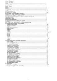

You also want an ePaper? Increase the reach of your titles
YUMPU automatically turns print PDFs into web optimized ePapers that Google loves.
F <strong>19</strong> <strong>SERVICE</strong> <strong>MANUAL</strong><br />
THIS DOCUMENT IS A PROPERTY<br />
OF INDUSTRIE FORMENTI ITALIA<br />
NO AUTHORIZED MODIFICATIONS<br />
ARE PERMITTED.<br />
CREATED BY E.G.
There are two different types of F<strong>19</strong> chassis that are equipped with two<br />
different microcontroller.<br />
These microcontroller are known as ETT having a code SAA5297A and<br />
PAINTER with a code number SAA5553.<br />
From the point of view of the application on the F<strong>19</strong> chassis the two type of<br />
microcontroller are substantially having the same performances, the same pinout<br />
, the same firmware but they are not interchangeable as the power supply<br />
are different.<br />
In case of SAA5297A the power supply is 5 V for the SAA5553 is 3.3 V.<br />
Even if the two devices are non interchangeable the two chassis<br />
can be interchanged as the in/out interface are exactly the same.<br />
As the specifications of the two devices are the same and the first version of<br />
the chassis was equipped with the SAA5297A , in this document the<br />
characteristics of it are very much detailed meanwhile there is a very short<br />
description (as an addendum at the end) for the SAA5553.
F<strong>19</strong> CHASSIS DESCRIPTION<br />
Summary<br />
The F<strong>19</strong> is a chassis suitable to drive CRT having both 4 by 3 and 16 to 9 aspect<br />
ratio and dimension from 25" up to 34".<br />
As we can see from the block diagram the chassis is equipped with the most recent<br />
Integrated Circuit like the one chip TV processor TDA884x that does include all the low<br />
level signal processing including Video, Audio, synchronisation process, and chroma<br />
decoder . (see more detail at the "TDA884x FAMILY SPECIFICATION" paragraph), and<br />
the Sound Processor TDA9875A that perform all sound function including digital decoding<br />
of NICAM signals. (see more detail at the " TDA9870A & tda9875A MAIN<br />
CHARACTERISTICS" paragraph).<br />
The above mentioned devices are driven by an Integrated Circuit that does include<br />
the microcontroller function with 64 K ROM and the TELETEXT acquisition and 8 pages<br />
RAM. (SAA5297A)<br />
In the F<strong>19</strong> chassis there are, besides the stereo one, two possible module that are<br />
performing "FEATURES" like PIP (picture in picture) and / or CTI (colour transients<br />
improvement) and 4 by 3 to 16 by 9 signal processing. One further module is dedicated to<br />
the so called "Zero Power Stand By"<br />
A 26 Key Remote Control is performing the full control for the end- used but can<br />
also be used in " <strong>SERVICE</strong> MODE" to control and adjust, without open the back cover of<br />
the TV set all the necessary functions.<br />
With the 5 "LOCAL KEY BOARD" button all the end user function can also be<br />
performed<br />
When the TV set is equipped with a PLL tuner the microcontroller recognise it and<br />
the tuning method became a frequency synthesis system if not it work as a voltage tuning<br />
system (provided all necessary components are mounted)<br />
The TV make use of a multilevel MENU (activated both by the Remote Control and<br />
Local Keyboard) using five selectable languages ( Italian, German, English, France, end<br />
Spanish) with which it is possible to control sequentially all video and sound value, to<br />
adjust several parameter like picture format, sound response, sleep timer etc., and to set<br />
others important parameter like standard, select country for automatic tuning and sort etc.<br />
Here below a list of the characteristics of the TV se<br />
E.G.Data creazione 31/10/99 15.38 1 / 7 f<strong>19</strong>intro
TV SET CHARACTERISTICS (MONO & STEREO )<br />
PICTURE TUBE SIZE :<br />
• 4 : 3 ASPECT RATIO 21” / 25” / 28” / 29” / 34”<br />
• 16 : 9 ASPECT RATIO 28 “ / 32”<br />
• STANDARD<br />
• R.F. (ANTENNA) (FOR FREQ. SYNTH.) CCIR ( B / G/ L / L’ / D / K / I )<br />
• VIDEO (SCART & CINCH)<br />
B / G/ L / L’ / D / K / I / M / N<br />
• COLOUR (MAX. THREE STANDARDS)<br />
PAL / SECAM / NTSC<br />
• SOUND STANDARD:<br />
B / G/ L / L’ / D / K / I<br />
∗ MONO<br />
AM & FM<br />
∗ STEREO<br />
A2 OR NICAM<br />
TUNING SYSTEM SELECTABLE :<br />
FACTORY OPTION<br />
FREQUENCY SYTHETIZER<br />
• TOTAL AVAILABLE CHANNEL NUMBER 200<br />
• CHANNEL IN ONE RF STANDARD UP TO 100<br />
• NUMBER OF PROGRAM 100<br />
• DIRECT PROGRAM & CHANNEL CALL WITH 1, OR 2 OR 3 DIGIT<br />
• PROGRAM & CHANNEL STEP UP AND DOWN YES<br />
• VOLTAGE SYNTHESISER<br />
• CABLE & HYPERBAND CHANNEL<br />
YES<br />
• SWITCHABLE AFC<br />
YES<br />
• AUTOMATIC SEARCH TUNING<br />
YES<br />
• A S T WITH AUTO SORT<br />
YES<br />
AUDIO SECTION<br />
POWER<br />
• MONO<br />
6 W RMS.<br />
• STEREO<br />
2 x 6 W RMS.<br />
EXTERNAL CONNECTION<br />
• HEADPHONE<br />
STEREO SET ONLY<br />
• LOUDSPEAKERS<br />
INTERNAL L.S. SWITCHED<br />
A / V INPUT / OUTPUT<br />
• FRONT PANEL CINCH<br />
A / V INPUT<br />
• I FULL SCART (CVBS, STEREO, RBA)<br />
MULTIMEDIA INPUT OUTPUT<br />
• SCART (CVBS & STEREO IN / OUT)<br />
VCR, HI.FI, SATELLITE, ETC<br />
• SCART A TO SCART B LOOP THROUGH FOR PROGRAMS DUBBING<br />
TXT<br />
PANEUROPEAN CHARACTER SET<br />
• LEVEL 1<br />
8 PAGES<br />
• LEVEL 1,5 (FASTEXT)<br />
7 PAGES<br />
FEATURES<br />
• CTI (COLOUR TRANSIENT IMPROVEMENT) OPTION<br />
• 16:9 TO 4:3 VIDEO COMPRESSION<br />
ONLY FOR 16:9 TV SET<br />
• VERTICAL ZOOM OUT<br />
3 LEVEL<br />
• MENU DRIVEN SYSTEM<br />
• EASY TO USE REMOTE CONTROL<br />
• REMOTE CONTROL WITH “<strong>SERVICE</strong>” USE NOT ACCESSIBLE TO END USER<br />
• PIP<br />
OPTION<br />
E.G.Data creazione 31/10/99 15.38 2 / 7 f<strong>19</strong>intro
EEPROM<br />
PCF8582<br />
AUDIO<br />
A U D I O<br />
THIS MODULE IS PRESENT ONLY FOR STEREO SET<br />
2ND SCART<br />
A/V IN/OUT<br />
TDA9875<br />
SCART INTER.<br />
A /V OUT<br />
A/V IN<br />
AUDIO<br />
VIDEO<br />
&<br />
AUDIO<br />
FULL SCART<br />
RGB<br />
AUDIO<br />
TDA1521<br />
TUNER<br />
PLL<br />
MICRO<br />
PIP<br />
SIEMENS<br />
IIC bus<br />
PCA84C841/210<br />
TXT<br />
SAA5281/....<br />
SAA5297A<br />
T.O.P.<br />
PHILIPS<br />
SAW<br />
FILTER<br />
TXT & OSD<br />
R B G<br />
PIP (RGB)<br />
VIDEO PROCESSOR<br />
TDA 8362A<br />
TDA8395TDA844X<br />
S E C A M<br />
D.L. CROMA<br />
TDA4661<br />
POWER SUPPLY<br />
RGB<br />
RGB<br />
(OSD)<br />
VERTICAL<br />
TDA3654<br />
E.W. GEN.<br />
TDA4950<br />
H. DRIVER L.O.T.<br />
BU 508 D<br />
BC 639<br />
TDA 4605 & STH7N80F<br />
CUT-OFF<br />
E H T<br />
TRAFO<br />
V.<br />
H.<br />
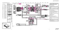
F16UPF<strong>19</strong>.DRW<br />
E.G. 2/02/99<br />
F16 UPDATED F<strong>19</strong> BLOCK DIAGRAM<br />
26 V<br />
12 V<br />
140 V<br />
15 V<br />
8 V<br />
VIDEO AMPL.<br />
TDA5112<br />
RGB<br />
EAT<br />
110°
F <strong>19</strong><br />
IIC bus<br />
IIC bus<br />
EEPROM<br />
PCF8584 /<br />
ST2404CB<br />
TUNER<br />
PLL<br />
IIC bus<br />
LOCAL KEY BOARD<br />
E T T<br />
MICROCONTROLLER<br />
& TELETEX 8 PAGES<br />
PIP<br />
OPTION<br />
PIP (RGB)<br />
VIDEO & AUDIO<br />
AUDIO STEREO (NICAM) PROCESSOR<br />
THIS MODULE IS PRESENT ONLY FOR STEREO SET<br />
TXT<br />
& OSD<br />
R B G<br />
I.R. INPUT<br />
F<strong>19</strong> BLOCK DIAGRAM<br />
V<br />
I<br />
D<br />
E<br />
O<br />
A<br />
U<br />
D<br />
I<br />
O<br />
I.<br />
F.<br />
SAW<br />
FILTER<br />
I<br />
NTERCARRIER<br />
SAA5297A<br />
TDA 9811 (nicam) TDA 9870A (TDA9875A (nicam)<br />
2ND SCART<br />
AUDIO<br />
A/V IN/OUT<br />
A /V OUT<br />
AUDIO<br />
VIDEOSCART<br />
SWITCH LA7955<br />
A/V IN<br />
*IF VIDEO & PLL DEM<br />
*AGC & AFC, MUTE<br />
*AUDIO PLL DEM<br />
*PAL/NTSC (SECAM) DEC.<br />
*B.B CHROMA DELAY LINE<br />
*FULL SCART INTERFACE.<br />
4<br />
TDA 8843(4)<br />
U V<br />
FEATURES MODULE<br />
TDA4566 (CTI)<br />
SAA4981 (16:9 TO 4:3)<br />
OPTION<br />
POWER SUPPLY<br />
H. DRIVER<br />
TDA 4605 & STH7N90F1<br />
AUDIO SCART SWITCH HEF4053<br />
BC 338<br />
RGB<br />
*H & V SYNC PROCESSIG<br />
*FULL IIC BUS CONTROLL FOR:<br />
*AUTO CUT-OFF<br />
*ALL ANALOGUE FUCTIONS<br />
*GEOMETRY CORRECTION<br />
*FEATURES INTERFACE<br />
E-W POWER<br />
BUK474200A<br />
H DRIVE<br />
A/V/ CINCH<br />
(OPTION)<br />
FULL SCART<br />
IIC BUS ONE CHIP VIDEO PROCESSOR<br />
E-W-<br />
E-W DRIVE COIL<br />
DRIVER<br />
TRAFO<br />
150 V<br />
26 V<br />
12 V<br />
8 V<br />
5 V<br />
RGB<br />
CUT-OFF<br />
VERTICAL<br />
TDA8351<br />
L.O.T.<br />
BU 508 D<br />
TDA1521<br />
RGB<br />
VERTICAL<br />
FEEDBACK<br />
2 x 7 W<br />
AUDIO POWER<br />
LINE OUT<br />
(OPTION)<br />
VIDEO AMPL.<br />
TDA5112<br />
V.<br />
H.<br />
H. DEFL.<br />
& E H T<br />
TRAFO<br />
HEADPHONE<br />
E-W LOAD COIL<br />
EAT<br />
CRT<br />
110°<br />
F<strong>19</strong>BLDIA.DRW<br />
E.G. 17 / 7 / 99
F <strong>19</strong>.1<br />
I<br />
IIC bus<br />
IIC bus<br />
EEPROM<br />
PCF8584 /<br />
ST2404CB<br />
TUNER<br />
PLL<br />
IIC bus<br />
LOCAL KEY BOARD<br />
E T T<br />
SAA5297A or<br />
SAA5553M3<br />
MICROCONTROLLER<br />
& 8 PAGES TELETEXT<br />
PIP<br />
OPTION<br />
PIP (RGB)<br />
VIDEO & AUDIO<br />
AUDIO STEREO (NICAM) PROCESSOR<br />
THIS MODULE IS PRESENT ONLY FOR STEREO SET<br />
TXT<br />
& OSD<br />
R B G<br />
I.R. INPUT<br />
F<strong>19</strong>.1 BLOCK DIAGRAM<br />
V<br />
I<br />
D<br />
E<br />
O<br />
A<br />
U<br />
D<br />
I<br />
O<br />
I.<br />
F.<br />
SAW<br />
FILTER<br />
NTERCARRIER<br />
TDA 9811 (nicam) TDA 9870A (TDA9875A (nicam)<br />
2ND SCART<br />
AUDIO<br />
A/V IN/OUT<br />
A /V OUT<br />
AUDIO<br />
VIDEOSCART<br />
SWITCH LA7955<br />
A/V IN<br />
*IF VIDEO & PLL DEM<br />
*AGC & AFC, MUTE<br />
*AUDIO PLL DEM<br />
*PAL/NTSC (SECAM) DEC.<br />
*B.B CHROMA DELAY LINE<br />
*FULL SCART INTERFACE.<br />
4<br />
TDA 8843 (4)<br />
U V<br />
FEATURES MODULE<br />
TDA4566 (CTI)<br />
SAA4981 (16:9 TO 4:3)<br />
OPTION<br />
POWER SUPPLY<br />
H. DRIVER<br />
BC 338<br />
TDA 4605 & STH7N90F1<br />
AUDIO SCART SWITCH HEF4053<br />
150 V<br />
26 V<br />
12 V<br />
8 V<br />
5 V<br />
RGB<br />
*H & V SYNC PROCESSIG<br />
*FULL IIC BUS CONTROLL FOR:<br />
*AUTO CUT-OFF<br />
*ALL ANALOGUE FUCTIONS<br />
*GEOMETRY CORRECTION<br />
*FEATURES INTERFACE<br />
E-W-<br />
E-W POWER<br />
BUK474200A<br />
H DRIVE<br />
A/V/ CINCH<br />
(OPTION)<br />
FULL SCART<br />
IIC BUS ONE CHIP VIDEO PROCESSOR<br />
DRIVER<br />
TRAFO<br />
RGB<br />
CUT-OFF<br />
VERTICAL<br />
TDA8351<br />
E-W DRIVE COIL<br />
L.O.T.<br />
BU 508 D<br />
TDA1521<br />
RGB<br />
VERTICAL<br />
FEEDBACK<br />
2 x 7 W<br />
AUDIO POWER<br />
LINE OUT<br />
(OPTION)<br />
VIDEO AMPL.<br />
TDA5112<br />
V.<br />
H.<br />
H. DEFL.<br />
& E H T<br />
TRAFO<br />
HEADPHONE<br />
E-W LOAD COIL<br />
EAT<br />
CRT<br />
110°<br />
F<strong>19</strong>BDE&P.DRW<br />
E.G. 22/04/2000
F<strong>19</strong> TUNING<br />
&<br />
TELETEXT
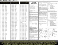
SAA529XA FAMILY MAIN CHARACTERISTICS<br />
FEATURES<br />
General<br />
• Single chip microcontroller with integrated teletext decoder<br />
• Single +5 V power supply<br />
• Single crystal oscillator for teletext decoder, display and microcontroller<br />
• Teletext function can be powered-down independent of microcontroller function for<br />
reduced power consumption in standby<br />
• Pin compatibility throughout family.<br />
Microcontroller<br />
• 80C51 microcontroller core<br />
• 16/32/64 kbyte mask programmed ROM<br />
• 256/768/1280 bytes of microcontroller RAM<br />
• Eight 6-bit Pulse Width Modulator (PWM) outputs for control of TV analog signals<br />
• One 14-bit PWM for Voltage Synthesis Tuner control<br />
• Four 8-bit Analog-to-Digital converters<br />
• 2 high current open-drain outputs for directly driving LEDs etc.<br />
• I 2 C-bus interface<br />
• External ROM and RAM capability on QFP80 package version.<br />
Teletext acquisition<br />
• 1 page and 10 page Teletext version<br />
• Acquisition of 525-line and 625-line World System Teletext, with automatic selection<br />
• Acquisition and decoding of VPS data (PDC system A)<br />
• Page clearing in under 64 s (1 TV line)<br />
• Separate storage of extension packets (SAA5296/7, SAA5296/7A and SAA5496/7)<br />
• Inventory of transmitted Teletext pages stored in the Transmitted Page Table (TPT)<br />
end Subtitle Page Table (SPT) (SAA5296/7, SAA5296/7A and SAA5496/7)<br />
• Automatic detection of FASTEXT transmission<br />
E.G.Data creazione 01/11/99 17.27 8 / 30 F<strong>19</strong>MANU.doc
TO CURRENT INTEGRATOR<br />
VOLTAGE SINTESYS ONLY<br />
MENU V - V + P - P +<br />
SAA5297A.DRW<br />
E.G . 17 / 10 / 99<br />
TO X13<br />
FRANCE STD. SWITCH<br />
CTI DETECTOR<br />
16 : 9 DETECTOR<br />
SCART1 / SCART2 SWITCH<br />
SCART 1 / TV<br />
TO SCART 2 SWITCH<br />
FRONT CINCH / SCART1<br />
SWITCH<br />
SCART 1 INPUT DETECTOR<br />
SCART 2 INPUT DETECTOR<br />
HEAD PHONES DETECTOR<br />
STANDARD SWITCH<br />
UHF SUPPLY<br />
(VOLTAGE SINTESYS ONLY)<br />
TV / AV SWITCH<br />
LOCAL KEY BOARD<br />
TV ON / OFF SWITCH<br />
TUNER SUPPLY (V.S. ONLY)<br />
TUNER SUPPLY(V.S. ONLY)<br />
CVBS FROM ANTENNA<br />
CVBS FROM SCART<br />
DATA<br />
SLICER<br />
REF.PIN<br />
SAA5297A<br />
1<br />
2<br />
3<br />
4<br />
5<br />
6<br />
7<br />
8<br />
9<br />
10<br />
11<br />
12<br />
13<br />
14<br />
15<br />
16<br />
17<br />
18<br />
<strong>19</strong><br />
20<br />
21<br />
22<br />
23<br />
24<br />
25<br />
26<br />
V TUN.<br />
DSC<br />
SWT. L/L'<br />
CTI STS.<br />
16:9 STS<br />
SWT. S1/S2<br />
COPY SWT.<br />
SWT. CI/S1<br />
AV1 STS.<br />
AV2 STS.<br />
H.P. STS.<br />
SYSTEM<br />
VSS M+T<br />
UHF<br />
TV / AV<br />
P0.3<br />
P0.4<br />
P0.5<br />
ON / OFF<br />
VHF H<br />
VHF L<br />
VSSA<br />
CVBS0<br />
CVBS1<br />
BLACK<br />
IREF<br />
P<br />
O<br />
R<br />
T<br />
2<br />
P<br />
O<br />
R<br />
T<br />
3<br />
P<br />
O<br />
R<br />
T<br />
0<br />
PAGE<br />
RAM<br />
MICRO & TXT Block Diagram<br />
ROM RAM TIMER<br />
A/ D<br />
PWM<br />
TXT<br />
INT<br />
B<br />
U<br />
S<br />
T X T DATA<br />
SLICER &<br />
ACQUISITION<br />
P<br />
O<br />
R<br />
T<br />
1<br />
8051<br />
CORE<br />
OSCILLATOR<br />
DISPLAY<br />
TIMING<br />
DISPLAY<br />
SWT 16:9<br />
OSC. SWT.<br />
MSDA<br />
MSCL<br />
SDA 1<br />
INTO<br />
SCL 1<br />
AM/FM<br />
VDDM<br />
RESET<br />
OSCOUT<br />
OSCIN<br />
OSCGND<br />
VDDT<br />
VDDA<br />
VSYNC<br />
HSYNC<br />
BLK<br />
R<br />
G<br />
B<br />
RGBREF<br />
PIP STS<br />
INT. TEST<br />
FRAME<br />
52<br />
51<br />
50<br />
49<br />
48<br />
47<br />
46<br />
45<br />
44<br />
43<br />
42<br />
41<br />
40<br />
39<br />
38<br />
37<br />
36<br />
35<br />
34<br />
33<br />
32<br />
31<br />
30<br />
29<br />
28<br />
27<br />
TO CHANGE<br />
ASPECT RATIO<br />
TO SWITCH S.C.<br />
FROM 4.43<br />
TO 3.58 MHz<br />
I.R.<br />
5 V from ST-BY<br />
QZ100<br />
12 MHz<br />
MAIN<br />
IIC BUS<br />
IIC BUS<br />
FOR<br />
EEPROM<br />
SOUND STANDARD<br />
SWITCH<br />
FROM<br />
RESESET CIRCUIT<br />
5 V<br />
VERTICAL<br />
FLYBACK<br />
HORIZONTAL<br />
FLYBACK PULSE<br />
TO<br />
TDA884X<br />
RGB REFERENCE<br />
2,5 VVOLTAGE<br />
PIP DETECTOR<br />
NOT CONNECTED<br />
NOT CONNECTED
TO CURRENT INTEGRATOR<br />
VOLTAGE SINTESYS ONLY<br />
MENU V - V + P - P +<br />
LOCAL KEY BOARD<br />
TO X13<br />
FRANCE STD. SWITCH<br />
CTI DETECTOR<br />
16 : 9 DETECTOR<br />
SCART1 / SCART2 SWITCH<br />
SCART 1 / TV<br />
TO SCART 2 SWITCH<br />
FRONT CINCH / SCART1<br />
SWITCH<br />
SCART 1 INPUT DETECTOR<br />
SCART 2 INPUT DETECTOR<br />
HEAD PHONES DETECTOR<br />
STANDARD SWITCH<br />
UHF SUPPLY<br />
(VOLTAGE SINTESYS ONLY)<br />
TV / AV SWITCH<br />
TV ON / OFF SWITCH<br />
TUNER SUPPLY (V.S. ONLY)<br />
TUNER SUPPLY(V.S. ONLY)<br />
CVBS FROM ANTENNA<br />
CVBS FROM SCART<br />
SAA5553.DRW<br />
E.G 22/ 04 / 2000<br />
DATA<br />
SLICER<br />
REF.PIN<br />
SAA5553M3<br />
1<br />
2<br />
3<br />
4<br />
5<br />
6<br />
7<br />
8<br />
9<br />
10<br />
11<br />
12<br />
13<br />
14<br />
15<br />
16<br />
17<br />
18<br />
<strong>19</strong><br />
20<br />
21<br />
22<br />
23<br />
24<br />
25<br />
26<br />
V TUN.<br />
DSC<br />
SWT. L/L'<br />
CTI STS.<br />
16:9 STS<br />
SWT. S1/S2<br />
COPY SWT.<br />
SWT. CI/S1<br />
AV1 STS.<br />
AV2 STS.<br />
H.P. STS.<br />
SYSTEM<br />
VSS M+T<br />
UHF<br />
TV / AV<br />
P0.3<br />
P0.4<br />
P0.5<br />
ON / OFF<br />
VHF H<br />
VHF L<br />
VSSA<br />
CVBS0<br />
CVBS1<br />
BLACK<br />
IREF<br />
P<br />
O<br />
R<br />
T<br />
2<br />
P<br />
O<br />
R<br />
T<br />
3<br />
P<br />
O<br />
R<br />
T<br />
0<br />
PAGE<br />
RAM<br />
MICRO & TXT Block Diagram<br />
ROM RAM TIMER<br />
A/ D<br />
PWM<br />
TXT<br />
INT<br />
B<br />
U<br />
S<br />
T X T DATA<br />
SLICER &<br />
ACQUISITION<br />
8051<br />
CORE<br />
P<br />
O<br />
R<br />
T<br />
1<br />
OSCILLATOR<br />
DISPLAY<br />
TIMING<br />
DISPLAY<br />
SWT 16:9<br />
OSC. SWT.<br />
MSDA<br />
MSCL<br />
SDA 1<br />
INTO<br />
SCL 1<br />
AM/FM<br />
VDDM<br />
RESET<br />
OSCOUT<br />
OSCIN<br />
OSCGND<br />
VDDT<br />
VDDA<br />
VSYNC<br />
HSYNC<br />
BLK<br />
R<br />
G<br />
B<br />
RGBREF<br />
PIP STS<br />
INT. TEST<br />
FRAME<br />
52<br />
51<br />
50<br />
49<br />
48<br />
47<br />
46<br />
45<br />
44<br />
43<br />
42<br />
41<br />
40<br />
39<br />
38<br />
37<br />
36<br />
35<br />
34<br />
33<br />
32<br />
31<br />
30<br />
29<br />
28<br />
27<br />
TO CHANGE<br />
ASPECT RATIO<br />
TO SWITCH S.C.<br />
FROM 4.43<br />
TO 3.58 MHz<br />
I.R.<br />
5 V from ST-BY<br />
QZ100<br />
12 MHz<br />
MAIN<br />
IIC BUS<br />
IIC BUS<br />
FOR<br />
EEPROM<br />
SOUND STANDARD<br />
SWITCH<br />
FROM<br />
RESESET CIRCUIT<br />
3 V<br />
VERTICAL<br />
FLYBACK<br />
HORIZONTAL<br />
FLYBACK PULSE<br />
TO<br />
TDA884X<br />
RGB REFERENCE<br />
2,5 VVOLTAGE<br />
PIP DETECTOR<br />
NOT CONNECTED<br />
NOT CONNECTED
• Real-time packet 26 engine for processing accented (and other) characters<br />
• Comprehensive Teletext language coverage<br />
• Video signal quality detector.<br />
Teletext Display<br />
• 525-line and 625-line display<br />
• 12 10 character matrix<br />
• Double height, width and size On-Screen Display (OSD)<br />
• Definable border colour<br />
• Enhanced display features including meshing and shadowing<br />
• 260 characters in mask programmed ROM<br />
• Automatic FRAME output control with manual override<br />
• RGB push-pull output to standard decoder ICs<br />
• Stable display via slave synchronisation to horizontal sync and vertical sync.<br />
Additional features of SAA529xA devices<br />
• Wide Screen Signalling (WSS) bit decoding (line 23).<br />
2 GENERAL DESCRIPTION<br />
The SAA529x, SAA529xA and SAA549x family of microcontrollers are a derivative of the<br />
Philips’ industry-standard 80C51 microcontroller and are intended for use as the central<br />
control mechanism in a television receiver. They provide control functions for the television<br />
system and include an integrated teletext function.<br />
The teletext hardware has the capability of decoding and displaying both 525-line and 625-<br />
line World System Teletext. The same display hardware is used both for Teletext and On-<br />
Screen Display, which means that the display features give greater flexibility to<br />
differentiate the TV set.<br />
The family offers both 1 page and 10 page Teletext capability, in a range of ROM sizes.<br />
Increasing display capability is offered from the SAA5290 to the SAA5497.<br />
TELETEXT DECODER<br />
Data slicer<br />
E.G.Data creazione 01/11/99 17.27 9 / 30 F<strong>19</strong>MANU.doc
The data slicer extracts the digital teletext data from the incoming analog waveform. This<br />
is performed by sampling the CVBS waveform and processing the samples to extract the<br />
teletext data and clock.<br />
Acquisition timing<br />
The acquisition timing is generated from a logic level positive-going composite sync signal<br />
VCS. This signal is generated by a sync separator circuit which adaptively slices the sync<br />
pulses. The acquisition clocking and timing are locked to the VCS signal using a digital<br />
phase-locked-loop. The phase error in the acquisition phase-locked-loop is detected by a<br />
signal quality circuit which disables acquisition if poor signal quality is detected.<br />
Teletext acquisition<br />
This family is capable of acquiring 625-line and 525-line World System Teletext see “World<br />
System Teletext and Data Broadcasting System”. Teletext pages are identified by seven<br />
numbers: magazine (page hundreds), page tens, page units, hours tens, hours units,<br />
minutes tens and minutes units. The last four digits, hours and minutes, are known as the<br />
subcode, and were originally intended to be time related, hence their names.<br />
For the ten page device, each packet can only be written into one place in the teletext<br />
RAM so if a page matches more than one of the page requests the data is written into<br />
the area of memory corresponding to the lowest numbered matching page request.<br />
At power-up each page request defaults to any page, hold on and error check Mode 0.<br />
Rolling headers and time<br />
When a new page has been requested it is conventional for the decoder to turn the header<br />
row of the display green and to display each page header as it arrives until the correct<br />
page has been found.<br />
Error checking<br />
Before teletext packets are written into the page memory they are error checked. The error<br />
checking carried out depends on the packet number, the byte number, the error check<br />
mode bits in the page request data and the TXT1.8 BIT bit. If an uncorrectable error<br />
occurs in one of the Hamming checked addressing and control bytes in the page header<br />
or in the Hamming checked bytes in packet 8/30, bit 4 of the byte written into the memory<br />
is set, to act as an error flag to the software. If uncorrectable errors are detected in any<br />
other Hamming checked data the byte is not written into the memory.<br />
E.G.Data creazione 01/11/99 17.27 10 / 30 F<strong>19</strong>MANU.doc
Packet 26 processing<br />
One of the uses of packet 26 is to transmit characters which are not in the basic teletext<br />
character set. The family automatically decodes packet 26 data and, if a character<br />
corresponding to that being transmitted is available in the character set, automatically<br />
writes the appropriate character code into the correct location in the teletext memory. This<br />
is not a full implementation of the packet 26 specification allowed for in level 2 teletext, and<br />
so is often referred to as level 1.5.<br />
By convention, the packets 26 for a page are transmitted before the normal packets. To<br />
prevent the default character data overwriting the packet 26 data the device incorporates a<br />
mechanism which prevents packet 26 data from being overwritten.<br />
Fastext detection<br />
When a packet 27, designation code 0 is detected, whether or not it is acquired, the<br />
TXT13.FASTEXT bit is set. If the device is receiving 525-line teletext, a packet X/0/27/0 is<br />
required to set the flag. The flag can be reset by writing a logic 0 into the SFR bit.<br />
When a packet 8/30 is detected, or a packet 4/30 when the device is receiving a 525-line<br />
transmission, the TXT13.Pkt 8/30 is set. The flag can be reset by writing a logic 0 into the<br />
SFR bit.<br />
THE DISPLAY<br />
Introduction<br />
The capabilities of the display are based on the requirements of level 1 teletext, with some<br />
enhancements for use with locally generated on screen displays. The display consists of<br />
25 rows each of 40 characters, with the characters displayed being those from rows 0 to<br />
24 of the basic page memory. If the TXT7.STATUS ROW TOP bit is set row 24 is<br />
displayed at the top of the screen, followed by row 0, but normally memory rows are<br />
displayed in numerical order. The teletext memory stores 8 bit character codes which<br />
correspond to a number of displayable characters and control characters, which are<br />
normally displayed as spaces. The character set of the device is described in more detail<br />
below.<br />
E.G.Data creazione 01/11/99 17.27 11 / 30 F<strong>19</strong>MANU.doc
(OPTION BYTE 1<br />
BIT 3 SETTED TO 0<br />
EAST EUROPE<br />
CHARACTER SET<br />
NATIONAL OPTION FOR:<br />
POLISH<br />
GERMAN<br />
ESTONIAN<br />
SERBO-CROAT<br />
CZECH<br />
SLOVAKIA<br />
RUMANIAN<br />
WEST EUROPE<br />
CHARACTER SET<br />
NATIONAL OPTION FOR:<br />
ENGLISH<br />
GERMAN<br />
SWEDISH<br />
ITALIAN<br />
FREANCH<br />
SPANISH<br />
TURKISH<br />
(OPTION BYTE 1<br />
BIT 6 SETTED TO 1<br />
WEST<br />
F<strong>19</strong> E&WCS.DRW<br />
E.G. 7/11/99<br />
EAST<br />
D<br />
A<br />
PL<br />
CZ<br />
H<br />
Y<br />
R
Character matrix<br />
Each character is defined by a matrix 12 pixels wide and 10 pixels high. When displayed,<br />
each pixel is 1 12 s wide and 1 TV line, in each field, high.<br />
East/West selection<br />
In common with their predecessors, these devices store teletext pages as a series of 8 bit<br />
character codes which are interpreted as either control codes (to change colour, invoke<br />
flashing etc.) or displayable characters. When the control characters are excluded, this<br />
gives an addressable set of 212 characters at any given time.<br />
National option characters<br />
The meanings of some character codes between 20H and 7FH depend on the C12 to C14<br />
language control bits from the teletext page header.<br />
The interpretation of the C12 to C14 language control bits is dependent on the East/West<br />
bit.<br />
On-Screen Display characters<br />
Character codes 80H to 9FH are not addressed by the teletext decoding hardware. An<br />
editor is available to allow these characters to be redefined by the customer. The<br />
alternative character shapes in columns 8a and 9a (SAA549x only) can be displayed when<br />
the ‘graphics’ serial attribute is set. This increases the number of customer definable<br />
characters to 64.<br />
Clock generator<br />
The oscillator circuit is a single-stage inverting amplifier in a Pierce oscillator configuration.<br />
The circuitry between XTALIN and XTALOUT is basically an inverter biased to the transfer<br />
point. A crystal must be used as the feedback element to complete the oscillator circuitry.<br />
It is operated in parallel resonance. XTALIN is the high gain amplifier input and XTALOUT<br />
is the output. To drive the device externally XTALIN is driven from an external source and<br />
XTALOUT is left open-circuit.<br />
E.G.Data creazione 01/11/99 17.27 12 / 30 F<strong>19</strong>MANU.doc
SOUND I.F.<br />
AM<br />
SOUND<br />
FILTER<br />
12 V<br />
TUNUNG<br />
VOLTAGE<br />
TO PIN 2<br />
TUNER<br />
TO X13<br />
TR500<br />
F204<br />
TR2<strong>19</strong><br />
R174<br />
12V<br />
TR218<br />
5V<br />
CVBS PIN 6<br />
IC 204<br />
TO PIN 4 IC 201 R128<br />
TO PIN<br />
TO PIN 8 IC 201 R140 R141<br />
10, 11<br />
TR200<br />
IC 200<br />
TR110<br />
TR201<br />
FRON PIN 8 SCART 1<br />
F575<br />
TO PIN 1<br />
IC 204<br />
F576<br />
TR107<br />
TO STEREO<br />
NICAM<br />
MODULE<br />
T<br />
O<br />
T<br />
U<br />
N<br />
E<br />
R<br />
TO PIN 4<br />
IC 10<br />
PIN 5<br />
PIN 3<br />
PIN 4<br />
TR210<br />
TR2<br />
TR 502<br />
TR 501<br />
TR209<br />
TR503<br />
TR111<br />
FROM PIN 8 SCART 2<br />
5V<br />
R146<br />
MENU V - V + P - P +<br />
5V<br />
TO SWITC INT/EX SOUND<br />
TV ON / OFF<br />
CVBS FROM<br />
ANTENNA<br />
CVBS<br />
FROM SCART<br />
TR203<br />
TR211<br />
SAA5297A<br />
1<br />
2<br />
3<br />
4<br />
5<br />
6<br />
7<br />
8<br />
9<br />
10<br />
11<br />
12<br />
13<br />
14<br />
15<br />
16<br />
17<br />
18<br />
<strong>19</strong><br />
20<br />
21<br />
22<br />
23<br />
24<br />
25<br />
26<br />
V TUN.<br />
DSC<br />
SWT. L/L'<br />
CTI STS.<br />
16:9 STS<br />
SWT. S1/S2<br />
COPY SWT.<br />
SWT. CI/S1<br />
AV1 STS.<br />
AV2 STS.<br />
H.P. STS.<br />
SYSTEM<br />
VSS M+T<br />
UHF<br />
TV / AV<br />
P0.3<br />
P0.4<br />
P0.5<br />
ON / OFF<br />
VHF H<br />
VHF L<br />
VSSA<br />
CVBS0<br />
CVBS1<br />
BLACK<br />
IREF<br />
SWT 16:9<br />
OSC. SWT.<br />
MSDA<br />
MSCL<br />
SDA 1<br />
INTO<br />
SCL 1<br />
AM/FM<br />
VDDM<br />
RESET<br />
OSCOUT<br />
OSCIN<br />
OSCGND<br />
VDDT<br />
VDDA<br />
VSYNC<br />
HSYNC<br />
BLK<br />
R<br />
G<br />
B<br />
RGBREF<br />
PIP STS<br />
COR<br />
INT. TEST<br />
FRAME<br />
MICRO & TXT PERIPHERALS<br />
52<br />
51<br />
50<br />
49<br />
48<br />
47<br />
46<br />
45<br />
44<br />
43<br />
42<br />
41<br />
40<br />
39<br />
38<br />
37<br />
36<br />
35<br />
34<br />
33<br />
32<br />
31<br />
30<br />
29<br />
28<br />
27<br />
TO CTI &<br />
16:9 MOULE<br />
IIC BUS<br />
IRR100<br />
QZ100<br />
12 MHz<br />
TR 109<br />
IIC BUS<br />
TR206<br />
TR 205<br />
SOUND STDANDARD SWITCH<br />
TR 101<br />
TR 108<br />
R 106<br />
TR 102<br />
R167<br />
D 108<br />
TR 103<br />
D 105<br />
5V<br />
5V ST-BY<br />
FOR VOLTAGE<br />
SISTETIZER ONLY<br />
5 V<br />
TR 208<br />
3.58MHz<br />
EEPROM<br />
IC 101<br />
TR 105<br />
4.43 MHz<br />
TO PIN 10<br />
IC 102<br />
D 102 FLYBACK PULSE<br />
FROM EHT<br />
VERTICAL<br />
BLANKING<br />
FROM PIN 8<br />
IC 5<br />
TO PIN<br />
23, 24, 25<br />
IC 204<br />
F<strong>19</strong>MTPER.DRW<br />
E.G. 24 /10 /99<br />
TO<br />
PIN 35<br />
IC 204
TR200<br />
TR201<br />
SOUND I.F.<br />
AM<br />
SOUND<br />
FILTER<br />
F204<br />
CVBSPIN 6<br />
IC 204<br />
F575<br />
TO PIN 1<br />
IC 204<br />
F576<br />
TR107<br />
TO STEREO<br />
NICAM<br />
MODULE<br />
TO PIN 4<br />
IC 10<br />
PIN 5<br />
T<br />
O<br />
T<br />
U<br />
N<br />
E<br />
R<br />
PIN 3<br />
PIN 4<br />
12V<br />
TO PIN<br />
10, 11<br />
IC 200<br />
TR210<br />
TR2<br />
TR 502<br />
TR110<br />
TR 501<br />
TR218<br />
12 V<br />
TUNUNG<br />
VOLTAGE<br />
TO PIN 2<br />
TUNER<br />
5V<br />
TR2<strong>19</strong><br />
TO PIN 4 IC 201<br />
TO X13<br />
R174<br />
R128<br />
TR500<br />
TO PIN 8 IC 201 R140 R141<br />
TR209<br />
TR503<br />
TR111<br />
FRON PIN 8 SCART 1<br />
FROM PIN 8 SCART 2<br />
5V<br />
R146<br />
MENU V - V + P - P +<br />
5V<br />
TO SWITC INT/EX SOUND<br />
TV ON / OFF<br />
CVBS FROM<br />
ANTENNA<br />
CVBS<br />
FROM SCART<br />
TR203<br />
TR211<br />
SAA 5553<br />
1<br />
2<br />
3<br />
4<br />
5<br />
6<br />
7<br />
8<br />
9<br />
10<br />
11<br />
12<br />
13<br />
14<br />
15<br />
16<br />
17<br />
18<br />
<strong>19</strong><br />
20<br />
21<br />
22<br />
23<br />
24<br />
25<br />
26<br />
V TUN.<br />
DSC<br />
SWT. L/L'<br />
CTI STS.<br />
16:9 STS<br />
SWT. S1/S2<br />
COPY SWT.<br />
SWT. CI/S1AM/FM<br />
AV1 STS. VDDM<br />
AV2 STS. RESET<br />
H.P. STS. OSCOUT<br />
SYSTEM OSCIN<br />
VSS M+T<br />
UHF<br />
TV / AV<br />
P0.3<br />
P0.4<br />
P0.5<br />
ON / OFF<br />
VHF H<br />
VHF L<br />
VSSA<br />
CVBS0<br />
CVBS1<br />
BLACK<br />
IREF<br />
SWT 16:9<br />
OSC. SWT.<br />
MSDA<br />
MSCL<br />
SDA 1<br />
INTO<br />
SCL 1<br />
OSCGND<br />
VDDT<br />
VSSA<br />
VSYNC<br />
HSYNC<br />
BLK<br />
R<br />
G<br />
B<br />
RGBREF<br />
PIP STS<br />
COR<br />
INT. TEST<br />
FRAME<br />
MICRO & TXT PERIPHERALS<br />
52<br />
51<br />
50<br />
49<br />
48<br />
47<br />
46<br />
45<br />
44<br />
43<br />
42<br />
41<br />
40<br />
39<br />
38<br />
37<br />
36<br />
35<br />
34<br />
33<br />
32<br />
31<br />
30<br />
29<br />
28<br />
27<br />
TO CTI &<br />
16:9 MOULE<br />
IIC BUS<br />
IRR100<br />
QZ100<br />
12 MHz<br />
TR 109<br />
IIC BUS<br />
SOUND STDANDARD SWITCH<br />
TR 101<br />
TR 108<br />
TR 102<br />
R167<br />
D 108<br />
TR 103<br />
D 105<br />
3,3 V<br />
3,3 V<br />
D 102<br />
5V<br />
TR206<br />
TR 205<br />
TR8<br />
5 V<br />
FOR VOLTAGE<br />
SISTETIZER ONLY<br />
TR7<br />
D5<br />
TR 208<br />
3.58MHz<br />
EEPROM<br />
IC 101<br />
TR 105<br />
R39<br />
2,5V<br />
FLYBACK<br />
FROM EHT<br />
VERTICAL<br />
BLANKING<br />
FROM PIN 8<br />
IC 5<br />
TO PIN<br />
23, 24, 25<br />
IC 204<br />
F<strong>19</strong>PAPER.DRW<br />
E.G. 22 / 04 /2000<br />
4.43 MHz<br />
TO PIN 10<br />
IC 102<br />
5 V<br />
R40<br />
TO<br />
PIN 35<br />
IC 204<br />
PAINTER
VIDEO<br />
SIGNAL<br />
PROCESSING
F <strong>19</strong><br />
TO PIN 33<br />
IC100<br />
CVBS EF<br />
FOR TXT<br />
TO PIN 24<br />
TR203<br />
IC 100<br />
(CVBS FOR TXT)<br />
TO PIN 9<br />
IC 100<br />
AV1<br />
STATUS<br />
SCART 1<br />
FROM PIN 6<br />
IC100<br />
AV1 / AV2<br />
SWITCH<br />
FROM PIN 7<br />
IC100<br />
AV1 / TV<br />
SWITCH<br />
TO AV2<br />
<strong>19</strong><br />
8<br />
15<br />
11<br />
7<br />
16<br />
20<br />
CVBS IN<br />
TV<br />
CVBS<br />
TO PIN 10<br />
IC 100<br />
AV2 STATUS<br />
EF<br />
TR201<br />
EF<br />
TR204<br />
TR211<br />
1<br />
3<br />
EF<br />
TR200<br />
2<br />
EF<br />
4<br />
7<br />
IIC<br />
TR202<br />
EF<br />
VIDEO IN<br />
CINCH<br />
8<br />
12 V<br />
6<br />
5<br />
9<br />
1<br />
2<br />
3<br />
4<br />
5<br />
6<br />
7<br />
8<br />
9<br />
10<br />
11<br />
12<br />
13<br />
14<br />
15<br />
16<br />
17<br />
18<br />
<strong>19</strong><br />
20<br />
21<br />
22<br />
23<br />
24<br />
25<br />
26<br />
27<br />
28<br />
SIF<br />
AUDEXT<br />
NC<br />
NC<br />
PLLIF<br />
IFVIDEO OUT<br />
SCL<br />
SDA<br />
DECOUPLING<br />
CHR.IN<br />
EX.CVBS/Y IN<br />
VP1<br />
INT CVBS IN<br />
GND<br />
AUDIO OUT<br />
DECOUPLING<br />
EX. CVBS IN<br />
BLKIN<br />
B OUT<br />
G OUT<br />
R OUT<br />
BCL/VG<br />
R IN<br />
G IN<br />
B IN<br />
RGB INSERT.<br />
Y IN<br />
Y OUT<br />
1/3 0F IC201<br />
LA7955<br />
CVBS IN<br />
CVBS OUT<br />
FOR VOLTAGE SINTHESIS ONLY<br />
TDA884X<br />
I.F.<br />
VIDEO<br />
AGC<br />
AFC<br />
DEM.<br />
IDENT<br />
SOUND<br />
PROCES.<br />
(MONO)<br />
SYNC<br />
PROCES.<br />
V. & H.<br />
TIME<br />
BASE<br />
IIC<br />
TRANSRECEIVER<br />
TR212<br />
EF<br />
20 <strong>19</strong><br />
MSD<br />
PAL<br />
(SECAM)<br />
NTSC<br />
C.D. &<br />
RGB<br />
MATRIX<br />
VIDEO<br />
CONTROL<br />
8<br />
EXT RGB<br />
SWITCH<br />
& RGB<br />
DRIVE<br />
SCART 2<br />
DECOUPLING<br />
DEENPHASIS<br />
AGC OUT<br />
DECOPLING<br />
I REF<br />
VERT. RAMP<br />
EHT PROTEC.<br />
IF IN 2<br />
IF IN 1<br />
V. DRIVE A<br />
V. DRIVE B<br />
E - W OUT<br />
GND 2<br />
PH. 1 FILTER<br />
PH. 2 FILTER<br />
H. IN, S.C. OUT<br />
HOR. OUT<br />
DECOUPLING<br />
CVBS 1 OUT<br />
V P 2<br />
DET FILTER<br />
X TAL 2<br />
X TAL 1<br />
S.C. REF OUT<br />
R - Y IN<br />
B - Y IN<br />
R - Y OUT<br />
B - Y OUT<br />
56<br />
55<br />
54<br />
53<br />
52<br />
51<br />
50<br />
49<br />
48<br />
47<br />
46<br />
45<br />
44<br />
43<br />
42<br />
41<br />
40<br />
39<br />
38<br />
37<br />
36<br />
35<br />
34<br />
33<br />
32<br />
31<br />
30<br />
29<br />
EF<br />
RGB AMPLIFIER<br />
MODULE<br />
VIDEO SIGNAL PATH<br />
TO CRT<br />
8 V<br />
UV<br />
12 V<br />
IIC<br />
3,57MHz<br />
5 V<br />
1<br />
2<br />
3<br />
4<br />
5<br />
6<br />
7<br />
8<br />
9<br />
TR208<br />
3.58MHz<br />
TR206<br />
4.43MHz<br />
A10<br />
1<br />
2<br />
3<br />
4<br />
5<br />
6<br />
7<br />
8<br />
9<br />
10<br />
11<br />
12<br />
C T I<br />
&<br />
4 : 3<br />
TO<br />
16 : 9<br />
FROM PIN 52<br />
IC 100 4:3 TO 16:9<br />
SWITCH<br />
8 V<br />
TR500<br />
10<br />
11<br />
UHF<br />
VHF H<br />
VHF LTR502<br />
FROM PIN 1<br />
IC 100<br />
TR501<br />
5 V<br />
TR205<br />
FROM EHT<br />
TR503<br />
FROM IC 100<br />
PIN 14, 20, 21<br />
BAND SWITCHING<br />
TR105<br />
FROM<br />
PIN 51<br />
IC 100<br />
F<strong>19</strong>VIDEP.DRW<br />
E.G. 14 / 11 / 99
Reset signal<br />
The externally applied RESET signal (active HIGH) is used to initialize the microcontroller<br />
core, in addition to the teletext decoder. However, the teletext decoder incorporates a<br />
separate internal reset function which is activated on the rising edge of the analog supply<br />
pin, VDDA . The purpose of this internal reset circuit is to initialize the teletext decoder when<br />
returning from the “text standby mode”.<br />
TDA884X FAMILY SPECIFICATION<br />
FEATURES<br />
The following features are available in all IC’s:<br />
• Multi-standard vision IF circuit with an alignment-freePLL demodulator without external<br />
components<br />
• Alignment-free multi-standard FM sound demodulator(4.5 MHz to 6.5 MHz)<br />
• Audio switch<br />
• Flexible source selection with CVBS switch andY(CVBS)/C input so that a comb filter can<br />
be applied<br />
• Integrated chrominance trap circuit<br />
• Integrated luminance delay line<br />
• Asymmetrical peaking in the luminance channel with a(defeatable) noise coring function<br />
• Black stretching of non-standard CVBS or luminancesignals<br />
• Integrated chroma band-pass filter with switchablecentre frequency<br />
• Dynamic skin tone control circuit<br />
• Blue stretch circuit which offsets colours near whitetowards blue<br />
• RGB control circuit with “Continuous CathodeCalibration” and white point adjustment<br />
• Possibility to insert a “blue back” option when no videosignal is available<br />
• Horizontal synchronization with two control loops andalignment-free horizontal<br />
oscillatoroptimised N2 application.Functionally the IC series is split up is 3 categories,<br />
viz:<br />
E.G.Data creazione 01/11/99 17.27 13 / 30 F<strong>19</strong>MANU.doc
TUNER<br />
AGC<br />
I.F IN<br />
PLL<br />
FILTER<br />
Deenphasis<br />
EXTERNAL<br />
AUDIO IN<br />
A.F.<br />
54<br />
53<br />
48<br />
49<br />
5<br />
A<br />
F<br />
W<br />
AFA<br />
AFB<br />
2<br />
IF &<br />
TUNER<br />
A G C<br />
VIDEO IF<br />
AMPLIFIER<br />
A F C<br />
Sensitivity<br />
TDA 8844<br />
55<br />
15<br />
DEENPHASIS LINE<br />
Internal<br />
Audio<br />
EXTERNAL<br />
AUDIO<br />
SWITCH<br />
SWT<br />
MONO AUDIO OUTPUT<br />
TUNER T.O.P<br />
gating<br />
calibration<br />
I.F. value<br />
PLL<br />
DEMOD.<br />
& VCO<br />
VIDEO<br />
AMPLIFIER<br />
CVBS OUT<br />
CVBS (int) IN CVBS / Y IN (comb filter)<br />
CVBS OUTPUT CVBS (ext) IN CHROMA IN<br />
VIDEO<br />
IDENT.<br />
AVL<br />
SWITCH &<br />
VOLUME<br />
6<br />
MOD<br />
Pos./Neg.<br />
AVL<br />
Volume<br />
Y DELAY,<br />
C. TRAP,<br />
Y PEAKING<br />
VIDEO<br />
MUTE<br />
13 17 11 10 38<br />
Luma<br />
H. SYNC<br />
SEPARATOR<br />
AUDIO PRE<br />
AMPLIFIER<br />
& MUTE<br />
CVBS & Y/C<br />
SWITCH<br />
To Sync<br />
H. sync<br />
PHI 1<br />
DETECTOR<br />
Chroma<br />
CHROMA<br />
CLOCHE &<br />
BANDPASS<br />
V. SYNC<br />
SEPARATOR<br />
LINE<br />
OSCILL.<br />
VERTICAL<br />
DEVIDER<br />
V. sync<br />
SCL<br />
7 8<br />
IIC<br />
TRANS-<br />
RECEIVER<br />
IIC<br />
SDA<br />
PAL / NTSC<br />
SECAM<br />
DECODER<br />
AUTO<br />
SYSTEM<br />
IDENT.<br />
MANAGER<br />
VERTICAL<br />
SAWTOOTH<br />
GENERATOR<br />
Secam<br />
Decoupling<br />
SAT<br />
MAT<br />
DSA<br />
16<br />
CON<br />
BRI<br />
GAI<br />
Subcarrier<br />
Xtal<br />
34 35<br />
BURST PHASE<br />
DETECTOR<br />
& VCXO<br />
BASE BAND<br />
CHROMA<br />
DELAY LINE<br />
R-Y & B-Y<br />
MATRIX<br />
SAT CONTR.<br />
BLACK STRETCH<br />
SKIN TINT CORR.<br />
RGB SWITCH<br />
RGB CONTROL<br />
AUTO CUT-OFF<br />
& OUTPUT<br />
36<br />
33<br />
28<br />
29<br />
30<br />
27<br />
31<br />
Fsc<br />
Y<br />
B-Y<br />
R-Y<br />
Y<br />
B-Y<br />
32<br />
R-Y<br />
23<br />
R<br />
24<br />
G<br />
25<br />
B<br />
26 F.B.<br />
18<br />
<strong>19</strong><br />
20<br />
21<br />
Loop<br />
filter<br />
Phase<br />
Detector<br />
Black<br />
Currente<br />
Input<br />
R<br />
G<br />
B<br />
I<br />
N<br />
P<br />
U<br />
T<br />
O<br />
U<br />
T<br />
P<br />
U<br />
T<br />
AVL<br />
Decoupling<br />
INTER-<br />
CARRIER<br />
IN<br />
(45)<br />
1<br />
BandGap<br />
Decoupling<br />
1 A 10 MHz<br />
B.P.F.<br />
AUDIO<br />
LIMITER<br />
9 12 37 14<br />
8 V Main<br />
Supply<br />
8 V<br />
Supply<br />
Ground<br />
AUDIO<br />
PLL DEM.<br />
56<br />
Sound<br />
Decoupling<br />
43 42 41 40<br />
Phi 1<br />
filter<br />
Phi 2<br />
filter<br />
PHI 2<br />
LINE OUT<br />
S.C. GENER.<br />
Flyback in<br />
Sand<br />
Castle<br />
Out<br />
Line<br />
Pulse<br />
Out<br />
51 52<br />
E - W<br />
GEOMETRY<br />
45<br />
E-W<br />
Vertical<br />
DRIVE<br />
Sawtooth Reference<br />
50<br />
EHT<br />
Overvoltage<br />
VERTICAL<br />
DRIVE<br />
22<br />
47<br />
46<br />
Vertical<br />
Drive<br />
Output<br />
V- Guard &<br />
B.C. limiter<br />
TDA8844BLDIA.DRW<br />
E.G. 17 /10 / 99
• Versions intended to be used in economy TV receiverswith all basic functions (envelope:<br />
S-DIP 56 and QFP 64)<br />
• Versions with additional features like E-W geometrycontrol, H-V zoom function and YUV<br />
interface which are intended for TV receivers with 110° picture tubes(envelope: S-DIP 56)<br />
• Versions which have in addition a second RGB inputwith saturation control and a second<br />
CVBS output (envelope: QFP 64)<br />
• Vertical count-down circuit<br />
• Vertical driver optimised for DC-coupled vertical outputstages<br />
GENERAL DESCRIPTION<br />
The various versions of the TDA 884X/5X series areI 2 C-bus controlled single chip TV<br />
processors which are<br />
intended to be applied in PAL, NTSC, PAL/NTSC and multi-standard television receivers.<br />
The N2 version is pin and application compatible with the N1 version, however,a new<br />
feature has been added which makes the N2 more attractive. The IF PLL demodulator has<br />
been replaced byan alignment-free IF PLL demodulator with internal VCO (no tuned circuit<br />
required). The setting of the variousfrequencies (33.4, 33.9, 38, 38.9, 45,75 and 58.75<br />
MHz) can be made via the I 2 C-bus.<br />
Because of this difference the N2 version is compatiblewith the N1, however, N1 devices<br />
cannot be used in an optimized N2 application<br />
Functionally the IC series is split up is 3 categories, viz:<br />
• Versions intended to be used in economy TV receivers with all basic functions (envelope:<br />
S-DIP 56 and QFP 64)<br />
• Versions with additional features like E-W geometry control, H-V zoom function and YUV<br />
interface which areintended for TV receivers with 110° picture tubes (envelope: S-DIP 56)<br />
• Versions which have in addition a second RGB input with saturation control and a<br />
second CVBS output (envelope: QFP 64)<br />
FUNCTIONAL DESCRIPTION<br />
Vision IF amplifier<br />
The IF-amplifier contains 3 ac-coupled control stages with a total gain control range which<br />
is higher then 66 dB. The sensitivity of the circuit is comparable with that of modern<br />
E.G.Data creazione 01/11/99 17.27 14 / 30 F<strong>19</strong>MANU.doc
IF-IC’s.<br />
The video signal is demodulated by means of an alignment-free PLL carrier regenerator<br />
with an internalVCO. This VCO is calibrated by means of a digital control circuit which<br />
uses the X-tal frequency of the colour decoder as a reference. The frequency setting for<br />
the various standards (33.4, 33.9, 38, 38.9, 45.75 and 58.75 MHz) is realised via the I 2 C-<br />
bus. To get a good performance for phase modulated carrier signals the control speed of<br />
the PLL can be increased by means of the FFI bit.<br />
The AFC output is generated by the digital control circuit of the IF-PLL demodulator and<br />
can be read via the I 2 C-bus.<br />
For fast search tuning systems the window of the AFC can be increased with a factor 3.<br />
The setting is realised with the AFW bit. The AFC data is valid only when the horizontal<br />
PLL is in lock (SL = 1)<br />
Depending on the type the AGC-detector operates on top-sync level (single standard<br />
versions) or on top sync and top white- level (multi standard versions). The demodulation<br />
polarity is switched via the I 2 C-bus. The AGC detector time-constant capacitor is<br />
connected externally. This mainly because of the flexibility of the application. The timeconstant<br />
of the AGC system during positive modulation is rather long to avoid visible<br />
variations of the signal amplitude. To improve the speed of the AGC system a circuit has<br />
been included which detects whether the AGC detector is activated every frame period.<br />
When during 3 field periods no action detected the speed of the system is increased. For<br />
signals without peak white information the system switches automatically to a gated black<br />
level AGC. Because a black level clamp pulse is required for this way of operation the<br />
circuit will only switch to black level AGC in the internal mode.<br />
The circuits contain a video identification circuit which is independent of the<br />
synchronisation circuit. Therefore search tuning is possible when the display section of the<br />
receiver is used as a monitor. However, this ident circuit cannot be made as sensitive as<br />
the slower sync ident circuit (SL) and we recommend to use both ident outputs to obtain a<br />
reliable search system. The ident output is supplied to the tuning system via the I 2 C-bus.<br />
The input of the identification circuit is connected to pin 13 (S-DIP 56 devices), the<br />
“internal” CVBS input (see Fig.6).<br />
This has the advantage that the ident circuit can also be made operative when a<br />
scrambled signal is received (descrambler connected between pin 6 (IF video output) and<br />
pin 13). A second advantage is that the ident circuit can be used when the IF amplifier is<br />
not used (e.g. with built-in satellite tuners).<br />
E.G.Data creazione 01/11/99 17.27 15 / 30 F<strong>19</strong>MANU.doc
The video ident circuit can also be used to identify the selected CBVS or Y/C signal. The<br />
switching between the 2 modes can be realised with the VIM bit.<br />
Video switches<br />
The circuits have two CVBS inputs (internal and external CVBS) and a Y/C input. When<br />
the Y/C input is not required the Y input can be used as third CVBS input. The switch<br />
configuration is given in Fig.6. The selection of the various sources is made via the I 2 C-<br />
bus.<br />
For the TDA 884X devices the video switch configuration is identical to the switch of the<br />
TDA 8374/75 series. So the circuit has one CVBS output (amplitude of 2 VP-P for the<br />
TDA884X series) and the I 2 C-bus control is similar to that of the TDA 8374/75. For the<br />
TDA 885X IC’s the video switch circuit has a second output (amplitude of 1 VP-P ) which<br />
can be set independently of the position of the first output. The input signal for the decoder<br />
is also available on the CVBS1-output.<br />
Therefore this signal can be used to drive the Teletext decoder. If S-VHS is selected for<br />
one of the outputs the luminance and chrominance signals are added so that a CVBS<br />
signal is obtained again.<br />
Sound circuit<br />
The sound bandpass and trap filters have to be connected externally. The filtered<br />
intercarrier signal is fed to a limiter circuit and is demodulated by means of a PLL<br />
demodulator. This PLL circuit tunes itself automatically to the incoming carrier signal so<br />
that no adjustment is required.<br />
The volume is controlled via the I 2 C-bus. The deemphasis capacitor has to be connected<br />
externally. The non-controlled audio signal can be obtained from this pin (via a buffer<br />
stage).<br />
The FM demodulator can be muted via the I 2 C-bus. This function can be used to switchoff<br />
the sound during a channel change so that high output peaks are prevented.<br />
The TDA 8840/41/42/46 contain an Automatic Volume Levelling (AVL) circuit which<br />
automatically stabilises the audio output signal to a certain level which can be set by the<br />
viewer by means of the volume control. This function prevents big audio output fluctuations<br />
due to variations of the modulation depth of the transmitter. The AVL function can be<br />
activated via the I 2 C-bus.<br />
Synchronisation circuit<br />
E.G.Data creazione 01/11/99 17.27 16 / 30 F<strong>19</strong>MANU.doc
The sync separator is preceded by a controlled amplifier which adjusts the sync pulse<br />
amplitude to a fixed level. These pulses are fed to the slicing stage which is operating at<br />
50% of the amplitude. The separated sync pulses are fed to the first phase detector and to<br />
the coincidence detector. This coincidence detector is used to detect whether the line<br />
oscillator is synchronised and can also be used for transmitter identification. This circuit<br />
can be made less sensitive by means of the STM bit. This mode can be used during<br />
search tuning to avoid that the tuning system will stop at very weak input signals. The first<br />
PLL has a very high statical steepness so that the phase of the picture is independent of<br />
the line frequency.<br />
The horizontal output signal is generated by means of an oscillator which is running at<br />
twice the line frequency. Its frequency is divided by 2 to lock the first control loop to the<br />
incoming signal. The time-constant of the loop can be forced by the I 2 C-bus (fast or<br />
slow). If required the IC can select the time-constant depending on the noise content of the<br />
incoming video signal.<br />
The free-running frequency of the oscillator is determined by a digital control circuit which<br />
is locked to the reference signal of the colour decoder. When the IC is switched-on the<br />
horizontal output signal is suppressed and the oscillator is calibrated as soon as all subaddress<br />
bytes have been sent. When the frequency of the oscillator is correct the<br />
horizontal drive signal is switched-on. To obtain a smooth switching-on and switching-off<br />
behaviour of the horizontal output stage the horizontal output frequency is doubled during<br />
switch-on and switch-off (slow start/stop). During that time the duty cycle of the output<br />
pulse has such a value that maximum safety is obtained for the output stage.<br />
To protect the horizontal output transistor the horizontal drive is immediately switched off<br />
when a power-on-reset is detected. The drive signal is switched-on again when the normal<br />
switch-on procedure is followed, i.e. all sub-address bytes must be sent and after<br />
calibration the horizontal drive signal will be released again via the slow start procedure.<br />
When the coincidence detector indicates an out-of-lock situation the calibration procedure<br />
is repeated.<br />
The circuit has a second control loop to generate the drive pulses for the horizontal driver<br />
stage. The horizontal output is gated with the flyback pulse so that the horizontal output<br />
transistor cannot be switched-on during the flyback time.<br />
Via the I 2 C-bus adjustments can be made of the horizontal and vertical geometry. The<br />
vertical sawtooth generator drives the vertical output drive circuit which has a differential<br />
output current. For the E-W drive a single ended current output is available. A special<br />
E.G.Data creazione 01/11/99 17.27 17 / 30 F<strong>19</strong>MANU.doc
feature is the zoom function for both the horizontal and vertical deflection and the vertical<br />
scroll function which are available in some versions. When the horizontal scan is reduced<br />
to display 4:3 pictures on a 16:9 picture tube an accurate video blanking can be switched<br />
on to obtain well defined edges on the screen.<br />
Overvoltage conditions (X-ray protection) can be detected via the EHT tracking pin. When<br />
an overvoltage condition is detected the horizontal output drive signal will be switched-off<br />
via the slow stop procedure but it is also possible that the drive is not switched-off and that<br />
just a protection indication is given in the I 2 C-bus output byte.<br />
The choice is made via the input bit PRD. The IC’s have a second protection input on the<br />
ϕ2 filter capacitor pin. When this input is activated the drive signal is switched-off<br />
immediately and switched-on again via the slow start procedure. For this reason this<br />
protection input can be used as “flash protection”.<br />
The drive pulses for the vertical sawtooth generator are obtained from a vertical<br />
countdown circuit. This countdown circuit has various windows depending on the incoming<br />
signal (50 Hz or 60 Hz and standard or non standard). The countdown circuit can be<br />
forced in various modes by means of the I 2 C-bus. During the insertion of RGB signals<br />
the maximum vertical frequency is increased to 72 Hz so that the circuit can also<br />
synchronise on signals with a higher vertical frequency like VGA. To obtain short switching<br />
times of the countdown circuit during a channel change the divider can be forced in the<br />
search window by means of the NCIN bit. The vertical deflection can be set in the deinterlace<br />
mode via the I 2 C bus. To avoid damage of the picture tube when the vertical<br />
deflection fails the guard output current of the TDA 8350/51 can be supplied to the beam<br />
current limiting input. When a failure is detected the RGB-outputs are blanked and a bit is<br />
set (NDF) in the status byte of the I 2 C-bus. When no vertical deflection output stage is<br />
connected thisguard circuit will also blank the output signals. This can be overruled by<br />
means of the EVG bit.<br />
Chroma and luminance processing<br />
The circuits contain a chroma bandpass and trap circuit. The filters are realised by means<br />
of gyrator circuits and<br />
they are automatically calibrated by comparing the tuning frequency with the X-tal<br />
frequency of the decoder. The luminance delay line and the delay for the peaking circuit<br />
are also realised by means of gyrator circuits. The centre frequency of the chroma<br />
bandpass filter is switchable via the I 2 C-bus so that the performance can be optimised for<br />
E.G.Data creazione 01/11/99 17.27 18 / 30 F<strong>19</strong>MANU.doc
“front-end” signals and external CVBS signals. During SECAM reception the centre<br />
frequency of the chroma trap is reduced to get a better suppression of the SECAM carrier<br />
frequencies. All IC’s have a black stretcher circuit which corrects the black level for<br />
incoming video signals which have a deviation between the black level and the blanking<br />
level (back porch). The timeconstant for the black stretcher is realised internally.<br />
The resolution of the peaking control DAC has been increased to 6 bits. All IC’s have a<br />
defeatable coringfunction in the peaking circuit. Some of these IC’s have a YUV interface<br />
(see table on page 2) so that picture improvement IC’s like the TDA 9170 (Contrast<br />
improvement), TDA 9177 (Sharpness improvement) and TDA 4556/66 (CTI) can be<br />
applied. When the CTI IC’s are applied it is possible to increase the gain of the luminance<br />
channel by means of the GAI bit in subaddress 03 so that the resulting RGB output signals<br />
are not affected.<br />
Colour decoder<br />
Depending on the IC type the colour decoder can decode PAL, PAL/NTSC or<br />
PAL/NTSC/SECAM signals. The PAL/NTSC decoder contains an alignment-free X-tal<br />
oscillator, a killer circuit and two colour difference demodulators. The 90° phase shift for<br />
the reference signal is made internally.<br />
The IC’s contain an Automatic Colour Limiting (ACL) circuit which is switchable via the I 2<br />
C-bus and which prevents that oversaturation occurs when signals with a high chroma-toburst<br />
ratio are received. The ACL circuit is designed such that it only reduces the chroma<br />
signal and not the burst signal. This has the advantage that the colour sensitivity is not<br />
affected by this function. The SECAM decoder contains an auto-calibrating PLL<br />
demodulator which has two references, viz: the 4.4 MHz sub-carrier frequency which is<br />
obtained from the X-tal oscillator which is used to tune the PLL to the desired free-running<br />
frequency and the bandgap reference to obtain the correct absolute value of the output<br />
signal. The VCO of the PLL is calibrated during each vertical blanking period, when the IC<br />
is in search or SECAM mode.<br />
The frequency of the active X-tal is fed to the Fsc output (pin 33) and can be used to tune<br />
an external comb filter (e.g. the SAA 4961).<br />
The base-band delay line (TDA 4665 function) is integrated in the PAL/SECAM IC’s and in<br />
the NTSC IC TDA 8846A. In the latter IC it improves the cross colour performance<br />
(chroma comb filter). The demodulated colour difference signals are internally supplied to<br />
the delay line. The colour difference matrix switches automatically between PAL/SECAM<br />
and NTSC, however, it is also possible to fix the matrix in the PAL standard.<br />
E.G.Data creazione 01/11/99 17.27 <strong>19</strong> / 30 F<strong>19</strong>MANU.doc
The “blue stretch” circuit is intended to shift colour near “white” with sufficient contrast<br />
values towards more blue to obtain a brighter impression of the picture.<br />
Which colour standard the IC’s can decode depends on the external X-tals. The X-tal to be<br />
connected to pin 34 must have a frequency of 3.5 MHz (NTSC-M, PAL-M or PAL-N) and<br />
pin 35 can handle X-tals with a frequency of 4.4 and 3.5 MHz. Because the X-tal frequency<br />
is used to tune the line oscillator the value of the X-tal frequency must be given to the IC<br />
via the I 2 C-bus. It is also possible to use the IC in the so called “Tri-norma” mode for<br />
South America. In that case one X-tal must be connected to pin 34 and the other 2 to pin<br />
35. The switching between the 2 latter X-tals must be done externally. This has the<br />
consequence that the search loop of the decoder must be controlled by the µ-computer.<br />
To prevent calibration problems of the horizontal oscillator the external switching between<br />
the 2 X-tals should be carried out when the oscillator is forced to pin 34. For a reliable<br />
calibration of the horizontal oscillator it is very important that the X-tal indication bits (XA<br />
and XB) are not corrupted. For this reason the X-tal bits can be read in the output bytes so<br />
that the software can check the I 2 C-bus transmission.<br />
Under bad-signal conditions (e.g. VCR-playback in feature mode), it may occur that the<br />
colour killer is activated although the colour PLL is still in lock. When this killing action is<br />
not wanted it is possible to overrule the colour killer by forcing the colour decoder to the<br />
required standard and to activate the FCO-bit (Forced Colour On) in the control-5<br />
subaddress.<br />
The IC’s contain a so-called “Dynamic skin tone (flesh) control” feature. This function is<br />
realised in the YUV domain by detecting the colours near to the skin tone. The correction<br />
angle can be controlled via the I 2 C-bus.<br />
RGB output circuit and black-current stabilisation<br />
The colour-difference signals are matrixed with the luminance signal to obtain the RGBsignals.<br />
The TDA 884X devices have one (linear) RGB input. This RGB signal can be<br />
controlled on contrast and brightness (like TDA 8374/75). By means of the IE1 bit the<br />
insertion blanking can be switched on or off. Via the IN1 bit it can be read whether the<br />
insertion pin has a high level or not.<br />
The TDA 885X IC’s have an additional RGB input. This RGB signal can be controlled on<br />
contrast, saturation and brightness. The insertion blanking of this input can be switched-off<br />
by means of the IE2 bit. Via the IN2 bit it can be read whether the insertion pin has a high<br />
level or not.<br />
E.G.Data creazione 01/11/99 17.27 20 / 30 F<strong>19</strong>MANU.doc
The output signal has an amplitude of about 2 volts black-to-white at nominal input signals<br />
and nominal settings of the controls. To increase the flexibility of the IC it is possible to<br />
insert OSD and/or teletext signals directly at the RGB outputs. This insertion mode is<br />
controlled via the insertion input (pin 26 in the S-DIP 56- and pin 38 in the QFP-64<br />
envelope). This blanking action at the RGB outputs has some delay which must be<br />
compensated externally.<br />
To obtain an accurate biasing of the picture tube a “Continuous Cathode Calibration”<br />
circuit has been developed. This function is realised by means of a 2-point black level<br />
stabilisation circuit. By inserting 2 test levels for each gun and comparing the resulting<br />
cathode currents with 2 different reference currents the influence of the picture tube<br />
parameters like the spread in cut-off voltage can be eliminated.<br />
This 2-point stabilisation is based on the principle that the ratio between the cathode<br />
currents is coupled to the ratio between the drive voltages according to:<br />
[ I ki / I k2 ] = [ V dr1 / V dr2 ]<br />
The feedback loop makes the ratio between the cathode currents Ik1 and Ik2 equal to the<br />
ratio between the reference currents (which are internally fixed) by changing the (black)<br />
level and the amplitude of the RGB output signals via 2 converging loops. The system<br />
operates in such a way that the black level of the drive signal is controlled to the cut-off<br />
point of the gun so that a very good grey scale tracking is obtained. The accuracy of the<br />
adjustment of the black level is just dependent on the ratio of internal currents and these<br />
can be made very accurately in integrated circuits. An additional advantage of the 2-point<br />
measurement is that the control system makes the absolute value of Ik1 and Ik2 identical<br />
to the internal reference currents. Because this adjustment is obtained by means of an<br />
adaption of the gain of the RGB control stage this control stabilises the gain of the<br />
complete channel (RGB output stage and cathode characteristic).<br />
As a result variations in the gain figures during life will be compensated by this 2-point<br />
loop.<br />
An important property of the 2-point stabilisation is that the off-set as well as the gain of<br />
the RGB path is adjusted by the feedback loop. Hence the maximum drive voltage for the<br />
cathode is fixed by the relation between the test pulses, the reference current and the<br />
relative gain setting of the 3 channels. This has the consequence that the drive level of the<br />
CRT cannot be adjusted by adapting the gain of the RGB output stage. Because different<br />
picture tubes may require different drive levels the typical “cathode drive level” amplitude<br />
can be adjusted by means of an I 2 C-bus setting. Dependent on the chosen cathode drive<br />
E.G.Data creazione 01/11/99 17.27 21 / 30 F<strong>19</strong>MANU.doc
level the typical gain of the RGB output stages can be fixed taking into account the drive<br />
capability of the RGB outputs (pins <strong>19</strong> to 21). More details about the design will be given in<br />
the application report.<br />
The measurement of the “high” and the “low” current of the 2- point stabilisation circuit is<br />
carried out in 2 consecutive fields. The leakage current is measured in each field. The<br />
maximum allowable leakage current is 100 µA When the TV receiver is switched-on the<br />
RGB output signals are blanked and the black current loop will try to set the right picture<br />
tube bias levels. Via the AST bit a choice can be made between automatic start-up or a<br />
start-up via the µ-processor. In the automatic mode the RGB drive signals are switched-on<br />
as soon as the black current loop<br />
has been stabilised. In the other mode the BCF bit is set to 0 when the loop is stabilised.<br />
The RGB drive can than be switched-on by setting the AST bit to 0. In the latter mod some<br />
delay can be introduced between the setting of the BCF bit and the switching of the AST<br />
bit so that switch-on effects can be suppressed. It is also possible to start-up the devices<br />
with a fixed internal delay (as with the TDA 837X and the TDA884X/5X N1). This mode is<br />
activated with the BCO bit.<br />
The vertical blanking is adapted to the incoming CVBS signal (50 Hz or 60 Hz). When the<br />
flyback time of the vertical output stage is longer than the 60 Hz blanking time the blanking<br />
can be increased to the same value as that of the 50 Hz blanking. This can be set by<br />
means of the LBM bit.<br />
For an easy (manual) adjustment of the Vg2 control voltage the VSD bit is available. When<br />
this bit is activated the black current loop is switched-off, a fixed black level is inserted at<br />
the RGB outputs and the vertical scan is switched-off so that a horizontal line is displayed<br />
on the screen. This line can be used as indicator for the Vg2 adjustment. Because of the<br />
different requirements for the optimum cut-off voltage of the picture tube the RGB output<br />
level is adjustable when the VSD bit is activated. The control range is 2.5 ± 0.7 V and can<br />
be controlled via the brightness control DAC. It is possible to insert a so called “blue back”<br />
back-ground level when no video is available. This feature can be activated via the BB bit<br />
in the control2 subaddress.<br />
E.G.Data creazione 01/11/99 17.27 22 / 30 F<strong>19</strong>MANU.doc
F <strong>19</strong><br />
TO PIN 33<br />
IC100<br />
CVBS EF<br />
FOR TXT<br />
TO PIN 24<br />
TR203<br />
IC 100<br />
(CVBS FOR TXT)<br />
TO PIN 9<br />
IC 100<br />
AV1<br />
STATUS<br />
SCART 1<br />
FROM PIN 6<br />
IC100<br />
AV1 / AV2<br />
SWITCH<br />
FROM PIN 7<br />
IC100<br />
AV1 / TV<br />
SWITCH<br />
TO AV2<br />
<strong>19</strong><br />
8<br />
15<br />
11<br />
7<br />
16<br />
20<br />
CVBS IN<br />
TV<br />
CVBS<br />
TO PIN 10<br />
IC 100<br />
AV2 STATUS<br />
EF<br />
TR201<br />
EF<br />
TR204<br />
TR211<br />
1<br />
3<br />
EF<br />
TR200<br />
2<br />
EF<br />
4<br />
7<br />
IIC<br />
TR202<br />
EF<br />
VIDEO IN<br />
CINCH<br />
8<br />
12 V<br />
6<br />
5<br />
9<br />
1<br />
2<br />
3<br />
4<br />
5<br />
6<br />
7<br />
8<br />
9<br />
10<br />
11<br />
12<br />
13<br />
14<br />
15<br />
16<br />
17<br />
18<br />
<strong>19</strong><br />
20<br />
21<br />
22<br />
23<br />
24<br />
25<br />
26<br />
27<br />
28<br />
SIF<br />
AUDEXT<br />
NC<br />
NC<br />
PLLIF<br />
IFVIDEO OUT<br />
SCL<br />
SDA<br />
DECOUPLING<br />
CHR.IN<br />
EX.CVBS/Y IN<br />
VP1<br />
INT CVBS IN<br />
GND<br />
AUDIO OUT<br />
DECOUPLING<br />
EX. CVBS IN<br />
BLKIN<br />
B OUT<br />
G OUT<br />
R OUT<br />
BCL/VG<br />
R IN<br />
G IN<br />
B IN<br />
RGB INSERT.<br />
Y IN<br />
Y OUT<br />
1/3 0F IC201<br />
LA7955<br />
CVBS IN<br />
CVBS OUT<br />
FOR VOLTAGE SINTHESIS ONLY<br />
TDA884X<br />
I.F.<br />
VIDEO<br />
AGC<br />
AFC<br />
DEM.<br />
IDENT<br />
SOUND<br />
PROCES.<br />
(MONO)<br />
SYNC<br />
PROCES.<br />
V. & H.<br />
TIME<br />
BASE<br />
IIC<br />
TRANSRECEIVER<br />
TR212<br />
EF<br />
20 <strong>19</strong><br />
MSD<br />
PAL<br />
(SECAM)<br />
NTSC<br />
C.D. &<br />
RGB<br />
MATRIX<br />
VIDEO<br />
CONTROL<br />
8<br />
EXT RGB<br />
SWITCH<br />
& RGB<br />
DRIVE<br />
SCART 2<br />
DECOUPLING<br />
DEENPHASIS<br />
AGC OUT<br />
DECOPLING<br />
I REF<br />
VERT. RAMP<br />
EHT PROTEC.<br />
IF IN 2<br />
IF IN 1<br />
V. DRIVE A<br />
V. DRIVE B<br />
E - W OUT<br />
GND 2<br />
PH. 1 FILTER<br />
PH. 2 FILTER<br />
H. IN, S.C. OUT<br />
HOR. OUT<br />
DECOUPLING<br />
CVBS 1 OUT<br />
V P 2<br />
DET FILTER<br />
X TAL 2<br />
X TAL 1<br />
S.C. REF OUT<br />
R - Y IN<br />
B - Y IN<br />
R - Y OUT<br />
B - Y OUT<br />
56<br />
55<br />
54<br />
53<br />
52<br />
51<br />
50<br />
49<br />
48<br />
47<br />
46<br />
45<br />
44<br />
43<br />
42<br />
41<br />
40<br />
39<br />
38<br />
37<br />
36<br />
35<br />
34<br />
33<br />
32<br />
31<br />
30<br />
29<br />
EF<br />
RGB AMPLIFIER<br />
MODULE<br />
VIDEO SIGNAL PATH<br />
TO CRT<br />
8 V<br />
UV<br />
12 V<br />
IIC<br />
3,57MHz<br />
5 V<br />
1<br />
2<br />
3<br />
4<br />
5<br />
6<br />
7<br />
8<br />
9<br />
TR208<br />
3.58MHz<br />
TR206<br />
4.43MHz<br />
A10<br />
1<br />
2<br />
3<br />
4<br />
5<br />
6<br />
7<br />
8<br />
9<br />
10<br />
11<br />
12<br />
C T I<br />
&<br />
4 : 3<br />
TO<br />
16 : 9<br />
FROM PIN 52<br />
IC 100 4:3 TO 16:9<br />
SWITCH<br />
8 V<br />
TR500<br />
10<br />
11<br />
UHF<br />
VHF H<br />
VHF LTR502<br />
FROM PIN 1<br />
IC 100<br />
TR501<br />
5 V<br />
TR205<br />
FROM EHT<br />
TR503<br />
FROM IC 100<br />
PIN 14, 20, 21<br />
BAND SWITCHING<br />
TR105<br />
FROM<br />
PIN 51<br />
IC 100<br />
F<strong>19</strong>VIDEP.DRW<br />
E.G. 14 / 11 / 99
IC204 TDA884X<br />
26 23/24/25 <strong>19</strong>/20/21 18<br />
F<strong>19</strong> RGB AMPLIFIER<br />
12 V<br />
200 V<br />
TO G1 TRC<br />
RGB<br />
IN<br />
RGB<br />
OUT<br />
2<br />
3<br />
1<br />
FAST<br />
BLK.<br />
IN<br />
R17,R18,R<strong>19</strong><br />
RGB IN FROM SCART<br />
R215<br />
R216<br />
R217<br />
R600<br />
2<br />
6/11/14<br />
5<br />
D800, D801, D802<br />
9/12/15<br />
E.F.<br />
4 / 5 / 6<br />
R613<br />
R614<br />
R615<br />
1/3/4<br />
7/10/13<br />
TO<br />
RGB<br />
KATODE<br />
R604<br />
R605<br />
R606<br />
STV 5112<br />
F<strong>19</strong> RGBCO.DRW<br />
E.G. 14 / 11 /99<br />
3 X
F <strong>19</strong> FEATURE MODULE<br />
Colour Transient Improvment<br />
&<br />
4 : 3 to 16 : 9 Signal Processing
SAA4981<br />
Monolithic integrated 16 : 9<br />
Compressor<br />
FEATURES<br />
• Fixed horizontal compression by a factor of 4 ¤3 for most video standards<br />
• Three fixed screen positions (left, centre and right)<br />
• 5 MHz bandwidth<br />
• Bypass function<br />
• Inputs for luminance and chrominance of side panels<br />
• Standard video inputs and outputs (Y, (Β-Y) and (Ρ-Y))<br />
• Horizontal and vertical sync signals are not processed<br />
• Pre filters and post filters on chip.<br />
GENERAL DESCRIPTION<br />
The integrated 16 : 9 compressor is an IC which compresses the active part of a video line<br />
by a factor of 4 ¤3 from, for example, 52 ms to 39ms. This is necessary to display 4:3<br />
video software on a 16 : 9 tube in the correctproportion. The capacitively coupled video<br />
inputs are Y, (Β-Y) and (Ρ-Y).<br />
The synchronisation input HREF is a line frequencyreference signal. The bandwidth of the<br />
IC is up to 5 MHz and the signal delay is realized with SC Line Memories (Switched<br />
Capacitors Line Memories). The output of the 16 : 9 compressor also has the format Y,<br />
(Β Y) and (Ρ-Y) and provides the following two possibilities:<br />
1. Bypass function (the input signal is not compressed)<br />
2. Compressed video by a factor of 4 ¤3 with three different fixed screen positions (left,<br />
centre and right). The luminance and chrominance of the side panels are determined by<br />
the external signals YSIDE, BYSIDE and RYSIDE.<br />
The horizontal compression is a time discrete and amplitude continuous signal processing.<br />
This provides pre and post filters which are realized on-chip.<br />
FUNCTIONAL DESCRIPTION<br />
SAA4981 16:9 TO 4:3 PROCESSOR Pagina 1 di 3 e.g.SAA4981R.doc
V CCA<br />
V EEA<br />
V CCD<br />
V EED SUB<br />
20 <strong>19</strong> 8 7 4<br />
YIN<br />
23<br />
CLAMP<br />
5 MHz<br />
LOW-PASS FILTER<br />
SC LINE MEMORY<br />
SC LINE MEMORY<br />
MUX<br />
SC LINE<br />
MEMORIES<br />
6.7 MHz<br />
LOW-PASS FILTER<br />
MUX Y<br />
18<br />
YOUT<br />
SAA4981<br />
C1 C2 C3<br />
B-Y)IN<br />
22<br />
CLAMP<br />
5 MHz<br />
LOW-PASS FILTER<br />
SC LINE MEMORY<br />
SC LINE MEMORY<br />
MUX<br />
SC LINE<br />
MEMORIES<br />
6.7 MHz<br />
LOW-PASS FILTER<br />
MUX BY<br />
17<br />
(B-Y)OUT<br />
C1 C2 C3<br />
R-Y)IN<br />
21<br />
CLAMP<br />
5 MHz<br />
LOW-PASS FILTER<br />
SC LINE MEMORY<br />
SC LINE MEMORY<br />
MUX<br />
SC LINE<br />
MEMORIES<br />
6.7 MHz<br />
LOW-PASS FILTER<br />
MUX RY<br />
16<br />
(R-Y)OUT<br />
HREF<br />
6<br />
HORIZONTAL<br />
SEPARATION<br />
C1<br />
3<br />
C1 C2 C3<br />
54 MHz<br />
PLL<br />
CONTROLLER<br />
C2<br />
C3<br />
CLAMP REFERENCE<br />
3<br />
12<br />
9<br />
10<br />
11 1 2 3 24 5 15 14 13<br />
MHA277<br />
TEST CTRL2<br />
CTRL1 CTRL3<br />
pagewidth<br />
C LMY<br />
CLMBY<br />
C LMRY<br />
BGREFCLAOUT<br />
BYSIDE<br />
YSIDE RYSIDE
Applicable video standards<br />
The integrated 16 : 9 compressor can be used for the following video standards; B, C, D,<br />
G, H, I, K, K1, L, M and N. standards D, I, K, K1 and L will show a reducedvideo bandwidth<br />
above 5 MHz.<br />
Clamping circuit<br />
The clamping circuits clamp the video input signals Y, (Β-Y) and (Ρ-Y) to the DC level of<br />
the clamp reference signal fed from the clamp reference circuit. This is necessary to<br />
ensure that the input signals are in the correct input voltage range for the 5 MHz low-pass<br />
filters and the SC line memories.<br />
Internal pre filters<br />
Before the signals are sampled in the time discrete and amplitude continuous area, lowpass<br />
filtering is necessary to avoid any aliasing. Even if the inputs have already been lowpass<br />
filtered further filtering is advantageous for the electromagnetic compatibility (EMC).<br />
The same transfer function is used for all three low-pass filters because of the same<br />
bandwidth for the luminance and chrominance signals (up to 5 MHz)<br />
SC line memories<br />
After the low-pass filters the input signals are fed to the SC line memories. The signals are<br />
sampled at a clock frequency of 13.5 MHz. One video line later the signals are read with a<br />
clock frequency of 18 MHz in the compression mode. The result of the different clock<br />
frequencies is a horizontal compression by a factor of 4 ¤3 . The clocks and the horizontal<br />
starting pulses for the SC line memories are fed from the controller.<br />
Two line memories are required for each signal path because in the compression mode, in<br />
one video line the signals are sampled to the SC line memories with 13.5 MHz and one<br />
video line later the signals are read with 18 MHz. In the bypass mode, via the SC line<br />
memories, in one video line the signals are sampled with 13.5 MHz and one video line<br />
later the signals are read with 13.5 MHz.<br />
The SC line memories are suitable for signals with a bandwidth up to 5 MHz. With a<br />
multiplexer (MUX) behind the SC line memories, the sampled video signal is connected to<br />
the internal post filters.<br />
Output multiplexer MUX Y, MUX (Β-Y) and MUX (Ρ-Y)<br />
SAA4981 16:9 TO 4:3 PROCESSOR Pagina 2 di 3 e.g.SAA4981R.doc
The output multiplexers are controlled via C1 and C2 fed from the controller. The<br />
multiplexers are used to connect one of the four input signals to the output and, also,<br />
enable fast switching.<br />
The input signals of the multiplexers for one component<br />
• The output signal of the post filter<br />
• The uncompressed signal after the input clamping<br />
• The clamping reference signal<br />
• The signal for the side panel determined by YSIDE, BYSIDE and RYSIDE.<br />
The horizontal separation circuit<br />
The 54 MHz horizontal PLL is locked to the positive edge of the digital HREF signal, which<br />
is generated in the positive edge of the burst key of a sandcastle signal.<br />
54 MHz horizontal PLL<br />
The 13.5 MHz clock frequency for the sampling clock and the 18 MHz clock frequency for<br />
the reading clock are generated in the 54 MHz horizontal PLL. The 13.5 MHzclock and the<br />
18 MHz clock are line locked.<br />
Clamp reference<br />
Reference voltages are generated In the clamp reference block. These DC signals are<br />
used in the clamping circuits as input signals for the output multiplexers and as reference<br />
voltages for the SC line memories. Four external capacitors at the pins CLMY , CLMBY ,<br />
CLMRY and BGREF respectively are necessary to provide smoothing for the reference<br />
voltages. A black level reference signal is available at CLAOUT.<br />
Controller<br />
The controller generates the clocks and the horizontal start signals for the SC line<br />
memories and, also, the control signals for the output multiplexers. The timing for the start<br />
reading signal for three different screen positions (left, centre and right) and the control<br />
signals for the multiplexers (C1 and C2) is fixed. For the uncompressed signals a bypass<br />
via the SC line memories and a bypass not via the SC line memories is available. When<br />
the signals do not pass the line memories, the frequencyresponse is not affected by the sifunction.<br />
SAA4981 16:9 TO 4:3 PROCESSOR Pagina 3 di 3 e.g.SAA4981R.doc
HREF<br />
1.5 µs<br />
1.5 µs<br />
64 µs<br />
sampled video<br />
(2)<br />
(1)<br />
(2)<br />
49 µs (used for compression)<br />
6.3 µs<br />
52 µs<br />
side<br />
panel<br />
36.75 µs<br />
compressed video<br />
(centre position)<br />
side<br />
panel<br />
side<br />
panel<br />
compressed video<br />
(right position)<br />
compressed video<br />
(left position)<br />
side<br />
panel<br />
bypassed video<br />
(bypass via the Line Memories)<br />
bypassed video<br />
(2)<br />
(1)<br />
(2)<br />
(full bypass not through the Line Memories)<br />
MHA278
TDA4566<br />
Colour transient improvement circuit<br />
GENERAL DESCRIPTION<br />
The TDA4566 is a monolithic integrated circuit for colour-transient improvement (CTI) and<br />
luminance delay line in gyrator technique in colour television receivers.<br />
Features<br />
• Colour transient improvement for colour difference signals (R-Y) and (B-Y) with transient<br />
detecting-, storage- and switching stages resulting in high transients of colour difference<br />
output signals<br />
• A luminance signal path (Y) which substitutes the conventional Y-delay coil with an<br />
integrated Y-delay line<br />
• Switchable delay time from 550 ns to 820 ns in steps of 90 ns and additional fine<br />
adjustment of 37 ns<br />
• Two Y output signals; one of 180 ns less delay<br />
TDA4566 CTI Pagina 1 di 1<br />
e.g.TDA4566R.doc
F<strong>19</strong> CTI & 16:9 TO 4 : 3 COMPRESSOR<br />
6<br />
9<br />
8<br />
1<br />
2<br />
12 V<br />
Y<br />
R-Y<br />
B-Y<br />
IC2 TDA4566<br />
15 13<br />
THESHOLD SWT.<br />
14 10<br />
17<br />
1<br />
CLAMP<br />
dV/dt<br />
dV/dt<br />
GYRATOR<br />
DELAY CELLS<br />
7 x 90 ns<br />
INTEGRATOR<br />
& PULSE<br />
FORMER<br />
t = 180 ns<br />
SWT. &<br />
STORE<br />
SWT. &<br />
STORE<br />
2 3 4 5 6 9 18<br />
12<br />
11<br />
8<br />
7<br />
Y<br />
R-Y<br />
B-Y<br />
IC 1<br />
23<br />
22<br />
21<br />
6<br />
CLAMP<br />
CLAMP<br />
CLAMP<br />
HOR.<br />
SEPAR.<br />
SAA4981<br />
LPF<br />
LPF<br />
LPF<br />
54 MHz<br />
PLL<br />
LINE MEMORY<br />
LINE MEMORY<br />
LINE MEMORY<br />
LINE MEMORY<br />
LINE MEMORY<br />
LINE MEMORY<br />
CONTROLLER<br />
20 8<br />
MUX<br />
MUX<br />
MUX<br />
LPF<br />
LPF<br />
LPF<br />
MUX<br />
MUX<br />
MUX<br />
CLAMP<br />
REFERENCE<br />
18<br />
17<br />
16<br />
13<br />
14<br />
5 V<br />
Y OUT<br />
R-Y<br />
OUT<br />
B-Y<br />
OUT<br />
10<br />
7<br />
4<br />
3<br />
7 20 4 12 11 10 9 <strong>19</strong> 1 2 3 24 5<br />
15<br />
5<br />
11<br />
8 V<br />
R4<br />
S.C INPUT<br />
C10<br />
16<br />
14<br />
13<br />
DUAL MONOSTABLE<br />
MULTIVIBRATOR<br />
M.M.<br />
15<br />
JS 7<br />
JS 6<br />
JS 5<br />
8 16 1<br />
M.M.<br />
3 5<br />
10<br />
2<br />
H REF<br />
5 V<br />
T2<br />
EF<br />
C9<br />
R2<br />
IC 4 HEF 4538<br />
8 V<br />
D1<br />
TR1<br />
12 V<br />
16:9 TO 4:3 SWITCH SIGNAL<br />
note:<br />
If CTI ( IC 2 TDA4566 IS NOT<br />
PRESENT THAN JS 5, JS 6 & JS7<br />
MUST BE INSERTED<br />
F<strong>19</strong>FEAT.DRW<br />
E.G. 12/12/99<br />
12
SCANNING<br />
SECTION
TDA8351<br />
DC-coupled vertical deflection<br />
Circuit<br />
FEATURES<br />
Few external components<br />
Highly efficient fully DC-coupled vertical output bridge circuit<br />
Vertical flyback switch<br />
Guard circuit<br />
Protection against:<br />
• short-circuit of the output pins (7 and 4)<br />
• short-circuit of the output pins to VP<br />
• Temperature (thermal) protection<br />
• High EMC immunity because of common mode inputs<br />
• A guard signal in zoom mode.<br />
•<br />
GENERAL DESCRIPTION<br />
The TDA8351 is a power circuit for use in 9and 11 colour deflection systems for<br />
field frequencies of 50 to 120 Hz. The circuit provides a DC driven vertical deflection<br />
output circuit, operating as a highly efficient class G system.<br />
FUNCTIONAL DESCRIPTION<br />
The vertical driver circuit is a bridge configuration. The deflection coil is connected<br />
between the output amplifiers, which are driven in phase opposition. An external resistor<br />
(RM ) connected in series with the deflection coil provides internal feedback information.<br />
The differential input circuit is voltage driven. The input circuit has been adapted to enable<br />
it to be used with the TDA9150, TDA9151B, TDA9160A, TDA9162, TDA8366 and<br />
TDA8376 which deliver symmetrical current signals. An external resistor (RCON )<br />
connected between the differential input determines the output current through the<br />
deflection coil.<br />
TDA8351 VERTICAL OUTPUT Pagina 1 di 2 e.g.TDA8351R
The relationship between the differential input current and the output current is defined by:<br />
Idiff RCON =Icoil RM .<br />
The output current is adjustable from 0.5 A (p-p) to 3 A(p-p) by varying RM . The maximum<br />
input differential voltage is 1.8 V. In the application it is recommended that Vdiff = 1.5 V<br />
(typ). This is recommended because of the spread of input current and the spread in the<br />
value of RCON .<br />
The flyback voltage is determined by an additional supply voltage VFB . The principle of<br />
operating with two supply voltages (class G) makes it possible to fix the supply voltage VP<br />
optimum for the scan voltage and the second supply voltage VFB optimum for the flyback<br />
voltage. Using this method, very high efficiency is achieved.<br />
The supply voltage VFB is almost totally available as flyback voltage across the coil, this<br />
being possible due to the absence of a decoupling capacitor (not necessary, due to the<br />
bridge configuration). The output circuit is fully protected against the following:<br />
thermal protection<br />
• short-circuit protection of the output pins (pins 4 and 7)<br />
• short-circuit of the output pins to VP .<br />
A guard circuit VO(guard) is provided. The guard circuit is activated at the following<br />
conditions:<br />
• during flyback<br />
• during short-circuit of the coil and during short-circuit of the output pins (pins 4 and 7)<br />
to VP or ground<br />
• during open loop<br />
• when the thermal protection is activated. This signal can be used for blanking the<br />
picture tubescreen.<br />
TDA8351 VERTICAL OUTPUT Pagina 2 di 2 e.g.TDA8351R
th<br />
V P<br />
V FB<br />
V O(guard)<br />
7<br />
3 8<br />
6<br />
V P<br />
CURRENT<br />
SOURCE<br />
TDA8351<br />
V P<br />
V O(A)<br />
V O(A)<br />
I drive(pos)<br />
I drive(neg)<br />
1<br />
2<br />
I S<br />
I T<br />
I<br />
T<br />
V P<br />
9<br />
V I(fb)<br />
V<br />
I<br />
S<br />
V O(B)<br />
4<br />
V O(B)<br />
5<br />
GND<br />
MBC988- 1
PINNING<br />
SYMBOL PIN DESCRIPTION<br />
I drive(pos) 1 input power-stage (positive);<br />
includes I I(sb) signal bias<br />
I drive(neg) 2 input power-stage (negative);<br />
includes I I(sb) signal bias<br />
V P 3 operating supply voltage<br />
V O(B) 4 output voltage B<br />
GND 5 ground<br />
V FB 6 input flyback supply voltage<br />
V O(A) 7 output voltage A<br />
V O(guard) 8 guard output voltage<br />
V I(fb) 9 input feedback voltage<br />
handbook, 2 columns<br />
I drive(pos) 1<br />
I drive(neg)<br />
V P<br />
VO(B)<br />
GND<br />
V FB<br />
V O(A)<br />
VO(guard)<br />
V I(fb)<br />
2<br />
3<br />
4<br />
5<br />
6<br />
7<br />
8<br />
9<br />
TDA8351<br />
MBC989
IC 204<br />
TDA8844<br />
28 V<br />
146 V<br />
HEATER<br />
VOLTAGE<br />
11<br />
12<br />
1<br />
T 3<br />
EHT<br />
FOCUS<br />
20 mS<br />
IC 5 TDA8351<br />
1<br />
2<br />
3<br />
4<br />
5<br />
6<br />
7<br />
8<br />
9<br />
47 46 45 40<br />
64 /uS<br />
EF<br />
TR207<br />
TR12<br />
BUK474<br />
2<br />
TR15<br />
L20<br />
T 2<br />
4<br />
3<br />
L22<br />
D24<br />
C71<br />
L25<br />
D25<br />
VIDEO<br />
SUPPLAY<br />
LINE<br />
TR18<br />
BU508D<br />
LINEARITY<br />
PIN 3<br />
TDA8351<br />
200 V<br />
D 53<br />
50 V 7<br />
8<br />
PIN6<br />
TDA8351<br />
YOKE<br />
5 5<br />
L26 C52<br />
16 V C51<br />
9<br />
3<br />
6<br />
R35<br />
10<br />
C154<br />
VG2<br />
B.C.L.<br />
PIN22<br />
TDA8844<br />
PIN 50<br />
EHT P.<br />
<strong>SERVICE</strong><br />
FLYBACK<br />
PULSE TO:<br />
PIP<br />
TUNING<br />
OSD SYNC<br />
VERTICAL<br />
YOKE<br />
F<strong>19</strong> VERTICAL & LINE OUTPUT<br />
PLUS E-W CORRECTION<br />
F<strong>19</strong> V&HDF.DRW<br />
E.G. 27/12/99
1 3<br />
SCART 1<br />
6 2<br />
EF<br />
CVBS & INTERCARRIER OUT<br />
TR110<br />
EF<br />
TR202<br />
TR201<br />
TR210<br />
6<br />
55<br />
2<br />
SCART<br />
OUT<br />
EXT. IN<br />
TR525<br />
15<br />
10<br />
2<br />
1<br />
FROM PIN8<br />
IC 100<br />
SCART/CINCH<br />
SWITCH<br />
8 V<br />
R239<br />
F575<br />
IC 204<br />
TDA844X<br />
14<br />
12<br />
13<br />
AUDIO<br />
CINCH IN<br />
R208<br />
SOUND<br />
IF IN<br />
F576<br />
R242<br />
1<br />
15<br />
IC 400 TDA2613<br />
9 8 7 6 5 4 3 2 1<br />
11<br />
IC200 (2/3) HEF 4053<br />
FROM PIN 12<br />
IC100<br />
SAA5297A<br />
TR209<br />
AUDIO OUT<br />
TR575<br />
F<strong>19</strong> AUDIO MONO SIGNAL PATH<br />
28 V<br />
F<strong>19</strong>AMSPH.DRW<br />
E.G. 29/12799
TDA 9870A & TDA9875A MAIN CHARACTERISTICS<br />
FEATURES<br />
Demodulator and decoder section<br />
• Sound IF (SIF) input switch e.g. to select between terrestrial TV SIF and SAT SIF<br />
sources SIF AGC with 24 dB control range SIF 8-bit Analog-to-Digital Converter<br />
(ADC)<br />
• DQPSK demodulation for different standards, simultaneously with 1-channel FM<br />
demodulation NICAM decoding (B/G, I and L standard) Two-carrier<br />
multistandard FM demodulation (B/G, D/K and M standard<br />
• Decoding for three analog multi-channel systems (A2, A2+ and A2*) and satellite<br />
sound Optional AM demodulation for system L, simultaneously with NICAM<br />
• Programmable identification (B/G, D/K and M standard) and different identification<br />
times.<br />
• DSP section<br />
• Digital crossbar switch for all digital signal sources and destinations<br />
• Control of volume, balance, contour, bass, treble,<br />
• pseudo stereo, spatial, bass boost and soft-mute<br />
• Plop-free volume control<br />
• Automatic Volume Level (AVL) control<br />
• Adaptive de-emphasis for satellite<br />
• Programmable beeper<br />
• Monitor selection for FM/AM DC values and signals, with peak detection option I 2 S-bus<br />
interface for a feature extension (e.g. Dolby surround) with matrix, level adjust and<br />
mute.<br />
• Analog audio section<br />
• Analog crossbar switch with inputs for mono and stereo<br />
E.G.Data creazione 01/11/99 17.27 23 / 30 F<strong>19</strong>MANU.doc
• (also applicable as SCART 3 input), SCART 1<br />
• input/output, SCART 2 input/output and line output<br />
• User defined full-level/3 dB scaling for SCART outputs<br />
• Output selection of mono, stereo, dual A/B, dual A or Dual B<br />
• 20 kHz bandwidth for SCART-to-SCART copies<br />
• Standby mode with functionality for SCART copies<br />
• Dual audio digital-to-analog converter from DSP to analog crossbar switch, bandwidth<br />
15 kHz Dual audio ADC from analog inputs to DSP Two dual audio Digital-to-<br />
Analog Converters (DACs) for loudspeaker (Main) and headphone (Auxiliary) outputs;<br />
also applicable for L, R, C and S in the Dolby Pro Logic mode with feature extension.<br />
GENERAL DESCRIPTION<br />
The TDA9875A is a single-chip Digital TV Sound Processor (DTVSP) for analog and<br />
digital multi-channel sound systems in TV sets and satellite receivers.<br />
Supported standards<br />
The multistandard/multi-stereo capability of the TDA9875A is mainly of interest in Europe,<br />
but also in Hong Kong/Peoples Republic of China and South East Asia. This includes<br />
B/G, D/K, I, M and L standard. In other application areas there exists only subsets of those<br />
standard combinations otherwise only single standards are transmitted.<br />
M standard is transmitted in Europe by the American Forces Network (AFN) with European<br />
channel spacing (7 MHz VHF, 8 MHz UHF) and monaural sound. The AM sound of L/L’ standard<br />
is normally demodulated in the 1 st sound IF. The resulting AF signal has to be entered into the<br />
mono audio input of the TDA9875A. A second possibility is to use the internal AM demodulator<br />
stage, however this gives limited performance. Korea has a stereo sound system similar to Europe<br />
and is supported by the TDA9875A. Differences include deviation, modulation contents and<br />
identification. It is based on M standard.<br />
FUNCTIONAL DESCRIPTION<br />
Description of the demodulator and decoder section<br />
SIF INPUT<br />
E.G.Data creazione 01/11/99 17.27 24 / 30 F<strong>19</strong>MANU.doc
Two input pins are provided, SIF1 e.g. for terrestrial TV and SIF2 e.g. for a satellite tuner.<br />
For higher SIF signal levels the SIF input can be attenuated with an internal switchable<br />
10 dB resistor divider. As no specific filters are integrated, both inputs have the same<br />
specification giving flexibility in application. The selected signal is passed through an AGC<br />
circuit and then digitized by an 8-bit ADC operating at 24.576 MHz.<br />
AGC<br />
The gain of the AGC amplifier is controlled from the ADC output by means of a digital<br />
control loop employing hysteresis. The AGC has a fast attack behaviour to prevent ADC<br />
overloads and a slow decay behaviour to prevent AGC oscillations. For AM demodulation<br />
the AGC must be switched off. When switched off, the control loop is reset and fixed gain<br />
settings can be chosen from Table 15 (subaddress 0).<br />
MIXER<br />
The digitized input signal is fed to the mixers, which mix one or both input sound carriers<br />
down to zero IF. A 24-bit control word for each carrier sets the required frequency. Access<br />
to the mixer control word registers is via the I 2 C-bus. When receiving NICAM programs,<br />
a feedback signal is added to the control word of the second carrier mixer to establish a<br />
carrier-frequency loop.<br />
FM AND AM DEMODULATION<br />
An FM or AM input signal is fed via a band-limiting filter to a demodulator that can be used<br />
for either FM or AM demodulation. Apart from the standard (fixed) de-emphasis<br />
characteristic, an adaptive de-emphasis is available for encoded satellite programs. A<br />
stereo decoder recovers the left and right signal channels from the demodulated sound<br />
carriers. Both the European and Korean stereo systems are supported.<br />
FM IDENTIFICATION<br />
The identification of the FM sound mode is performed by AM synchronous demodulation of<br />
the pilot signal and narrow-band detection of the identification frequencies. The result is<br />
available via the I 2 C-bus interface. A selection can be made via the I 2 C-bus for B/G,<br />
D/K and M standard and for three different modes that represent different trade-offs<br />
between speed and reliability of identification.<br />
NICAM DEMODULATION<br />
The NICAM signal is transmitted in a DQPSK code at a bit rate of 728 kbit/s. The NICAM<br />
demodulator performs DQPSK demodulation and feeds the resulting bitstream and clock<br />
signal onto the NICAM decoder and, for evaluation purposes, to PCLK (pin 1) and NICAM<br />
E.G.Data creazione 01/11/99 17.27 25 / 30 F<strong>19</strong>MANU.doc
(pin 2). A timing loop controls the frequency of the crystal oscillator to lock the sampling<br />
rate to the symbol timing of the NICAM data.<br />
NICAM DECODER<br />
The device performs all decoding functions in accordance with the “EBU NICAM 728<br />
specification”. After locking to the frame alignment word, the data is descrambled by<br />
applying the defined pseudo-random binary sequence; the device will then synchronize to<br />
the periodic frame flag bit C0.<br />
The status of the NICAM decoder can be read out from the NICAM status register by the<br />
user. The OSB bit indicates that the decoder has locked to the NICAM data. The VDSP bit<br />
indicates that the decoder has locked to the NICAM data and that the data is valid sound<br />
data. The C4 bit indicates that the sound conveyed by the FM mono channel is identical to<br />
the sound conveyed by the NICAM channel. The error byte contains the number of sound<br />
sample errors, resulting from parity checking, that occurred in the past 128 ms period.<br />
NICAM AUTO-MUTE<br />
This function is enabled by setting bit AMUTE LOW subaddress 14 Upper and lower error<br />
limits may be defined by writing appropriate values to two registers in the I 2 C-bus section<br />
(subaddresses 16 and 17; . When the number of errors in a 128 ms period exceeds the<br />
upper error limit the auto-mute function will switch the output sound from NICAM to<br />
whatever sound is on the first sound carrier (FM or AM). When the error count is smaller<br />
than the lower error limit the NICAM sound is restored. The auto-mute function can be<br />
disabled by setting bit AMUTE HIGH. In this condition clicks become audible when the<br />
error count increases; the user will hear a signal of degrading quality.<br />
A decision to enable/disable the auto-muting is taken by the microcontroller based on an<br />
interpretation of the application control bits C1, C2, C3 and C4 and, possibly, any<br />
additional strategy implemented by the set maker in the microcontroller software.<br />
For NICAM L applications, it is recommended to demodulate AM sound in the first sound<br />
IF and connect the audio signal to the mono input of the TDA9875A. By setting the AMSEL<br />
bit subaddress 14. the auto-mute function will switch to the audio ADC instead of switching<br />
to the first sound carrier.<br />
CRYSTAL OSCILLATOR<br />
The digital-controlled crystal oscillator (DCXO) is illustrated in Fig.8 (see Chapter 12). The<br />
circuitry of the DCXO is fully integrated, only the external 24.576 MHz crystal is needed.<br />
E.G.Data creazione 01/11/99 17.27 26 / 30 F<strong>19</strong>MANU.doc
TEST PINS<br />
Both test pins are active HIGH, in normal operation of the device they are wired to VSSD1<br />
Test functions are for manufacturing tests only and are not available to customers. Without<br />
external circuitry these pads are pulled down to LOW level with internal resistors.<br />
POWER FAIL DETECTOR<br />
The power fail detector monitors the internal power supply for the digital part of the device.<br />
If the supply has temporary been lower than the specified lower limit, the power-on reset<br />
bit POR, transmitter register subaddress 0 will be set to HIGH. The CLRPOR bit, slave<br />
register subaddress 1 resets the power-on reset flip-flop to LOW. If this is detected, an<br />
initialization of the TDA9875A has to be carried out to ensure reliable operation.<br />
LEVEL SCALING<br />
All input channels to the digital crossbar switch (except for the loudspeaker feedback path)<br />
are equipped with a level adjust facility to change the signal level in a range of 15 dB. It<br />
is recommended to scale all input channels to be 15 dB below full scale (15 dB full scale)<br />
under nominal conditions.<br />
NICAM PATH<br />
The NICAM path has a switchable J17 de-emphasis.<br />
FM (AM) PATH<br />
A high-pass filter suppresses DC offsets from the FM demodulator due to carrier frequency<br />
offsets and supplies the monitor/peak function with DC values and an unfiltered signal, e.g.<br />
for the purpose of carrier detection. The de-emphasis function offers fixed settings for the<br />
supported standards (50 µs, 60 µs 75 µs and J17). An adaptive de-emphasis is available<br />
for Wegener-Panda 1 encoded programs. A matrix performs the dematrixing of the A2<br />
stereo, dual and mono signals.<br />
NICAM AUTO-MUTE<br />
If NICAM B/G, I, D/K is received, the auto-mute is enabled and the signal quality becomes<br />
poor, the digital crossbar switch switches automatically to FM and switches the matrix to<br />
channel 1. The automatic switching depends on the NICAM bit error rate.<br />
The auto-mute function can be disabled via the I 2 C-bus. For NICAM L applications, it is<br />
recommended to demodulate AM sound in the first sound IF and connect the audio signal<br />
to the mono input of the TDA9875A. By setting the AMSEL bit subaddress 14 (see Section<br />
10.3.11), the auto-mute function will switch to the audio ADC instead of switching to the<br />
E.G.Data creazione 01/11/99 17.27 27 / 30 F<strong>19</strong>MANU.doc
first sound carrier. The ADC source selector subaddress 23 (see Section 10.3.20) should<br />
be set to mono input, where the AM sound signal should be connected.<br />
LOUDSPEAKER (MAIN) CHANNEL<br />
The matrix provides the following functions; forced mono, stereo, channel swap, channel<br />
1, channel 2 and spatial effects.<br />
There are fixed coefficient sets for spatial settings of 30%, 40% and 52%.<br />
The Automatic Volume Level (AVL) function provides a constant output level of 23 dB full<br />
scale for input levels between 0 and 29 dB full scale. There are some fixed decay time<br />
constants to choose from, i.e. 2, 4 and 8 seconds.<br />
Pseudo stereo is based on a phase shift in one channel via a 2 nd -order all-pass filter.<br />
There are fixed coefficient sets to provide 90 degrees phase shift at frequencies of 150,<br />
200 and 300 Hz.<br />
Volume is controlled individually for each channel ranging from +24 to -83 dB with 1 dB<br />
resolution. There is also a mute position. For the purpose of a simple control software in<br />
the microcontroller, the decimal number that is sent as an I 2 C-bus data byte for volume<br />
control is identical to the volume setting in dBs (e.g. the I 2 C-bus data byte +10 sets the<br />
new volume value to +10 dB).<br />
Balance can be realized by independent control of the left and right channel volume<br />
settings.<br />
Contour is adjustable between 0 and +18 dB with 1 dB resolution. This function is linked to<br />
the volume setting by means of microcontroller software.<br />
Bass is adjustable between +15 and -12 dB with 1 dB resolution and treble is adjustable<br />
between +/-12 dB with 1 dB resolution.<br />
For the purpose of a simple control software in the microcontroller, the decimal number<br />
that is sent as an I 2 C-bus data byte for contour, bass or treble is identical to the new<br />
contour, bass or treble setting in dBs (e.g. the I 2 C-bus data byte +8 sets the new value to<br />
+8 dB). Extra bass boost is provided up to 20 dB with 2 dB resolution. The implemented<br />
coefficient set serves merely as an example on how to use this filter.<br />
The beeper provides tones in a range from approximately 400 Hz to 30 kHz. The<br />
frequency can be selected via the I 2 C-bus. The beeper output signal is added to<br />
theloudspeaker and headphone channel signals. The beeper volume is adjustable with<br />
E.G.Data creazione 01/11/99 17.27 28 / 30 F<strong>19</strong>MANU.doc
espect to full scale between 0 and 93 dB with 3 dB resolution. The beeper is not<br />
effected by mute.<br />
Soft-mute provides a mute ability in addition to volume control with a well defined time (32<br />
ms) after which the soft-mute is completed. A smooth fading is achieved by a cosine<br />
masking.<br />
HEADPHONE (AUXILIARY) CHANNEL<br />
The matrix provides the following functions; forced mono, stereo, channel swap, channel<br />
and channel 2 (or C and S in Dolby Surround Pro Logic mode). Volume is controlled<br />
individually for each channel in a range from +24 to 83 dB with 1 dB resolution. There is<br />
also a mute position. For the purpose of a simple control software in the microcontroller,<br />
the decimal number that is sent as an I 2 C-bus data byte for volume control is identical to<br />
the volume setting in dB (e.g. the I 2 C-bus data byte +10 sets the new volume value to<br />
+10 dB). Balance can be realized by independent control of the left and right channel<br />
volume settings.<br />
Bass is adjustable between +15 and -12 dB with 1 dB resolution and treble is adjustable<br />
between +/- 12 dB with 1 dB resolution.<br />
For the purpose of a simple control software in the microcontroller, the decimal number<br />
that is sent as an I 2 C-bus data byte for bass or treble is identical to the new bass or<br />
treble setting in dB (e.g. the I 2 C-bus data byte +8 sets the new value to +8 dB).<br />
The beeper provides tones in a range from approximately 400 Hz to 30 kHz. The<br />
frequency can be selected via the I 2 C-bus. The beeper output signal is added to the<br />
loudspeaker and headphone channel signals. The beeper volume is adjustable with<br />
respect to full scale between 0 and 93 dB with 3 dB resolution. The beeper is not<br />
effected by mute.<br />
Soft-mute provides a mute ability in addition to volume control with a well defined time (32<br />
ms) after which the soft-mute is completed. A smooth fading is achieved by a cosine<br />
masking.<br />
SCART INPUTS<br />
The SCART specification allows for a signal level of up to 2 V (rms). Because of signal<br />
handling limitations, due to the 5 V supply voltage of the TDA9875A, it is necessary to<br />
have fixed 3 dB attenuators at the SCART inputs to obtain a 2 V input. This results in a +3<br />
dB SCART-to-SCART copy gain. If 0 dB copy gain is preferred (with maximum 1.4V input),<br />
there are +3 dB/0 dB amplifiers at the outputs of SCART 1 and SCART 2 and at the line<br />
E.G.Data creazione 01/11/99 17.27 29 / 30 F<strong>19</strong>MANU.doc
output. The input attenuator is realized by an external series resistor in combination with<br />
the input impedance, both of which form a voltage divider. With this voltage divider the<br />
maximum SCART signal level of 2 V (rms) is scaled down to 1.4 V (rms) at the input pin.<br />
EXTERNAL AND MONO INPUTS<br />
The 3 dB input attenuators are not required for the external and mono inputs, because<br />
those signal levels are under control of the TV designer. The maximum allowed input level<br />
is 1.4 V (rms). By adding external series resistors, the external inputs can be used as an<br />
additional SCART input.<br />
SCART OUTPUTS<br />
The SCART outputs employ amplifiers with two gain settings. The gain can be set to +3<br />
dB or to 0 dB via the I 2 C-bus. The +3 dB position is needed to compensate for the 3 dB<br />
attenuation at the SCART inputs should SCART-to-SCART copies with 0 dB gain be<br />
preferred [under the condition of 1.4 V (rms) maximum input level]. The 0 dB position is<br />
needed, for example, for an external-to-SCART copy with 0 dB gain.<br />
LINE OUTPUT<br />
The line output can provide an unprocessed copy of the audio signal in the loudspeaker<br />
channels. This can be either an external signal that comes from the dual audio ADC, or a<br />
signal from an internal digital audio source that comes from the dual audio DAC. The line<br />
output employs amplifiers with two gain settings. The +3 dB position is needed to<br />
compensate for the attenuation at the SCART inputs, while the 0 dB position is needed, for<br />
example, for non-attenuated external or internal digital signals (see Section 6.3.4).<br />
E.G.Data creazione 01/11/99 17.27 30 / 30 F<strong>19</strong>MANU.doc
TO PIN 9 IC1<br />
TDA9811<br />
TR8<br />
INTERCARRIER<br />
EF<br />
FROM PIN 20 IC1<br />
TDA9811<br />
6 V<br />
TO L/L' FILTER<br />
SWITCH<br />
TR8<br />
AM AUDIO<br />
FROM PIN 22 IC1<br />
TDA9811<br />
II S<br />
IIC BUS<br />
STD SWITCH<br />
TR6<br />
EF<br />
L /L' SWITCH<br />
1<br />
2<br />
3<br />
4<br />
5<br />
6<br />
7<br />
8<br />
9<br />
10<br />
11<br />
12<br />
13<br />
14<br />
15<br />
16<br />
17<br />
18<br />
<strong>19</strong><br />
20<br />
21<br />
22<br />
23<br />
24<br />
25<br />
26<br />
27<br />
28<br />
29<br />
30<br />
31<br />
32<br />
PLCK<br />
NICAM<br />
ADDR1<br />
SCL<br />
SDA<br />
VSSA1<br />
VDEC1<br />
Iref<br />
P1<br />
SIF2<br />
Vref<br />
SIF1<br />
ADDR2<br />
Vssd1<br />
Vdd1<br />
CRESET<br />
Vssd4<br />
XTAL1<br />
XTAL0<br />
P2<br />
SYSLCK<br />
SCK<br />
WS<br />
SDO2<br />
SDO1<br />
SDI2<br />
SDI1<br />
TEST1<br />
MONOIN<br />
TEST2<br />
EXT/R<br />
EXT/L<br />
IIC<br />
IN / OUT<br />
IDENT<br />
I / O<br />
PORT<br />
PEAK<br />
DETEC.<br />
VCXO<br />
CLOCK<br />
IIS<br />
ENC.<br />
DEC.<br />
FM DEM<br />
(AM DEM)<br />
DEMATR<br />
DEEMPH<br />
LEVEL<br />
ADJ.<br />
CHANNEL<br />
SELECTION<br />
QPSK<br />
DEM.<br />
NICAM<br />
DEC.<br />
LEVEL<br />
ADJ.<br />
AUDIO PROCESSING<br />
L.S.<br />
AVL,VOL<br />
CONTOUR<br />
BASS<br />
TREBLE<br />
PSEUDO<br />
BASS CORR<br />
DAC<br />
INPUT SWITCH<br />
AGC ADC<br />
DAC<br />
DAC<br />
H.P.<br />
VOL.<br />
BASS<br />
TREB.<br />
DAC<br />
TDA9875A<br />
ANALOGUE CROSS BAR SWITCH<br />
TEST<br />
VDD2<br />
LOR<br />
LOL<br />
MOL<br />
MOR<br />
Vdda<br />
AUXOL<br />
AUXOR<br />
Vssa3<br />
pcapl<br />
pcapr<br />
vREF3<br />
SCOL2<br />
SCOR2<br />
Vssa4<br />
Vssd2<br />
SCOL1<br />
SCOR2<br />
Vref2<br />
i.c.<br />
i.c.<br />
Vssa2<br />
i.c.<br />
i.c.<br />
Vref(n)<br />
Vref(p)<br />
Vdec2<br />
SCIL2<br />
SCIR2<br />
Vssd3<br />
SCIL1<br />
SCIR1<br />
TDA9875A PINOUT & PERIPHERALS<br />
64<br />
63<br />
62<br />
61<br />
60<br />
59<br />
58<br />
57<br />
56<br />
55<br />
54<br />
53<br />
52<br />
51<br />
50<br />
49<br />
48<br />
47<br />
46<br />
45<br />
44<br />
43<br />
42<br />
41<br />
40<br />
39<br />
38<br />
37<br />
36<br />
35<br />
34<br />
33<br />
AUDIO LINE OUT<br />
6 V<br />
TR11<br />
TR12<br />
TR9<br />
AUDIO OUT TO SCART<br />
AUDIO FROM SCART<br />
6 V<br />
TO AUDIO<br />
AMPLIFIER<br />
TR10<br />
TO HEADPHONES<br />
APLIFIER<br />
IC4<br />
TDA2822M<br />
TDA9875A.DRW<br />
E.G. 7/11/99
TDA9811<br />
Multistandard VIF-PLL<br />
with QSS-IF and AM demodulator<br />
FEATURES<br />
• 5 V supply voltage<br />
• Two switched VIF inputs, gain controlled wide band VIF-amplifier (AC-coupled)<br />
• True synchronous demodulation with active carrier regeneration (very linear<br />
demodulation, good intermodulation figures, reduced harmonics, excellent pulse<br />
response)<br />
• Gated phase detector for L/L accent standard VCO frequency switchable between L<br />
and L accent (alignment external) picture carrier frequency<br />
• Separate video amplifier for sound trap buffering with high video bandwidth VIF AGC<br />
detector for gain control, operating as peak sync detector for B/G (optional external<br />
AGC) and peak white detector for L; signal controlled reaction time for L<br />
• Tuner AGC with adjustable takeover point (TOP)<br />
• AFC detector without extra reference circuit<br />
• SIF input for single reference QSS mode (PLL controlled); SIF AGC detector for gain<br />
controlled SIF amplifier; single reference QSS mixer able to operate in high<br />
performance single reference QSS mode<br />
• AM demodulator without extra reference circuit<br />
• AM mute (especially for NICAM)<br />
• Stabilizer circuit for ripple rejection and to achieve constant output signals.<br />
GENERAL DESCRIPTION<br />
The TDA9811 is an integrated circuit for multistandard vision IF signal processing and<br />
sound AM demodulation, with single reference QSS-IF in TV and VCR sets.<br />
TDA9811 QSS Pagina 1 di 4 e.g. TDA9811R
h<br />
VIF input switch<br />
TOP<br />
tuner<br />
AGC<br />
loop<br />
filter<br />
2 x f PC<br />
AFC<br />
30 28 3 6<br />
<strong>19</strong><br />
7<br />
25<br />
24<br />
23<br />
TUNER AND VIF-AGC<br />
VCO TWD<br />
AFC DETECTOR<br />
VIFB<br />
VIFA<br />
SIF<br />
5<br />
4<br />
2<br />
1<br />
32<br />
31<br />
VIF AMPLIFIER<br />
AND<br />
INPUT SWITCH<br />
SIF<br />
AMPLIFIER<br />
FPLL<br />
SINGLE REFERENCE<br />
MIXER AND<br />
AM DEMODULATOR<br />
VIDEO DEMODULATOR<br />
AND AMPLIFIER<br />
TDA9811<br />
VIDEO<br />
BUFFER<br />
AF AMPLIFIER<br />
AND SWITCH<br />
21<br />
10<br />
22<br />
12<br />
video<br />
1 V (p-p)<br />
CVBS<br />
2 V (p-p)<br />
V i(vid)<br />
AF/AM<br />
INTERNAL VOLTAGE<br />
STABILIZER<br />
SIF-AGC<br />
29 27 26 9 8<br />
20 11 18 16 15 17<br />
13<br />
14<br />
n.c.<br />
n.c.<br />
1/2 V P<br />
5 V<br />
standard<br />
switch<br />
CAGC<br />
C AGC C BL<br />
MHA046<br />
(2nd SIF)<br />
V o QSS<br />
L′/L<br />
switch<br />
n.c.<br />
n.c.<br />
n.c.<br />
mute switch, AM
FUNCTIONAL DESCRIPTION<br />
Vision IF amplifier and input switch The vision IF amplifier consists of three AC-coupled<br />
differential amplifier stages. Each differential stage comprises a feedback network<br />
controlled by emitterdegeneration. T<br />
The first differential stage is extended by two pairs of emitter followers to provide two IF<br />
input channels. The VIF input can be selected by pin 30<br />
Tuner and VIF AGC<br />
The AGC capacitor voltage is transferred to an internal IF control signal, and is fed to the<br />
tuner AGC to generate the tuner AGC output current (open-collector output).<br />
The tuner AGC takeover point can be adjusted. This allows the tuner and the SWIF filter to<br />
be matched to achieve the optimum IF input level.<br />
The AGC detector charges/discharges the AGC capacitorto the required voltage for setting<br />
of VIF and tuner gain in order to keep the video signal at a constant level.<br />
Therefore for negative video modulation the sync level and for positive video modulation<br />
the peak white level of the video signal is detected. In order to reduce the reaction<br />
time for positive modulation, where a very large time constant is needed, an additional<br />
level detector increases the discharging current of the AGC capacitor (fast mode)<br />
in the event of a decreasing VIF amplitude step. The additional level information is given<br />
by the black-level detector voltage.<br />
Frequency Phase Locked Loop detector (FPLL)<br />
The VIF-amplifier output signal is fed into a frequency detector and into a phase detector<br />
via a limiting amplifier.<br />
During acquisition the frequency detector produces a DC current proportional to the<br />
frequency difference between the input and the VCO signal. After frequency lock-in the<br />
phase detector produces a DC current proportional to the phase difference between the<br />
VCO and the input signal. The DC current of either frequency detector or phase detector is<br />
converted into a DC voltage via the loop filter, which controls the VCO frequency. In the<br />
event of positive modulated signals the phase detector is gated by composite sync in order<br />
to avoid signal distortion for overmodulated VIF signals.<br />
TDA9811 QSS Pagina 2 di 4 e.g. TDA9811R
VCO, Travelling Wave Divider (TWD) and AFC<br />
The VCO operates with a resonance circuit (with L and C in parallel) at double the PC<br />
frequency. The VCO is controlled by two integrated variable capacitors.<br />
The control voltage required to tune the VCO from its free-running frequency to actually<br />
double the PC frequency is generated by the frequency-phase detector and fed via the<br />
loop filter to the first variable capacitor (FPLL). This control voltage is amplified and<br />
additionally converted into a current which represents the AFC output signal. The VCO<br />
centre frequency can be decreased (required for L accent standard) by activating an<br />
additional internal capacitor. This is achieved by using the L accent switch. In this event<br />
the second variable capacitor can be controlled by a variable resistor at the L accent<br />
switch for setting the VCO centre frequency to the required L accent value. At centre<br />
frequency the AFC output current is equal to zero.<br />
The oscillator signal is divided-by-two with a TWD which generates two differential output<br />
signals with a 90 degree phase difference independent of the frequency.<br />
Video demodulator and amplifier<br />
The video demodulator is realized by a multiplier which is designed for low distortion and<br />
large bandwidth. The vision IF input signal is multiplied with the ‘in phase’ signal of the<br />
travelling wave divider output. In the demodulator stage the video signal polarity can be<br />
switched in accordancewith the TV standard. The demodulator output signal is fed via an<br />
integrated low-pass filter for attenuation of the carrier harmonics to the video amplifier. The<br />
video amplifier is realized by an operational amplifier with internal feedback and high<br />
bandwidth. A low-pass filter is integrated to achieve an attenuation of the carrier harmonics<br />
for B/G and L standard. The standard dependent level shift in this stage delivers the same<br />
sync level for positive and negative modulation. The video output signal is 1 V (p-p) for<br />
nominal vision IF modulation.<br />
Video buffer<br />
For an easy adaption of the sound traps an operational amplifier with internal feedback is<br />
used in the event of B/G and L standard. This amplifier is featured with a high bandwidth<br />
and 7 dB gain. The input impedance is adapted output stage delivers a nominal 2 V (p-p)<br />
positive video signal. Noise clipping is provided.<br />
TDA9811 QSS Pagina 3 di 4 e.g. TDA9811R
SIF amplifier and AGC<br />
The sound IF amplifier consists of two AC-coupled differential amplifier stages. Each<br />
differential stage comprises a controlled feedback network provided by emitter<br />
degeneration. The SIF AGC detector is related to the SIF input signals (average level of<br />
AM or FM carriers) and controls the SIF amplifier to provide a constant SIF signal to the<br />
AM demodulator and single reference QSS mixer. The SIF AGC reaction time is set to<br />
‘slow’ for nominal video conditions. But with a decreasing VIF amplitude step the SIF AGC<br />
is set to ‘fast’ mode controlled by the VIF AGC detector. In FM mode this reaction time is<br />
also set to ‘fast’ controlled by the standard switch.<br />
Single reference QSS mixer The single reference QSS mixer is realized by a multiplier.<br />
The SIF amplifier output signal is fed to the single reference QSS mixer and converted to<br />
intercarrier frequency by the regenerated picture carrier (VCO).<br />
The mixer output signal is fed via a high-pass for attenuation of the video signal<br />
components to the output pin 20. With this system a high performance hi-fi stereo<br />
sound processing can be achieved.<br />
AM demodulator<br />
The AM demodulator is realized by a multiplier. The modulated SIF amplifier output signal<br />
is multiplied in phase with the limited (AM is removed) SIF amplifier output signal. The<br />
demodulator output signal is fed via an integrated low-pass filter for attenuation of the<br />
carrier harmonics to the AF amplifier.<br />
Internal voltage stabilizer and 1 ¤2 VP -reference<br />
The bandgap circuit internally generates a voltage of approximately 1.25 V, independent of<br />
supply voltage and temperature. A voltage regulator circuit, connected to this voltage,<br />
produces a constant voltage of 3.6 V which is used as an internal reference voltage.<br />
For all audio output signals the constant reference voltage cannot be used because large<br />
output signals are required.<br />
TDA9811 QSS Pagina 4 di 4 e.g. TDA9811R
PINNING<br />
SYMBOL PIN DESCRIPTION<br />
V i VIF1 1 VIF differential input signal voltage 1<br />
V i VIF2 2 VIF differential input signal voltage 2<br />
C BL 3 black level detector<br />
V i VIF3 4 VIF differential input signal voltage 3<br />
andbook, halfpage<br />
Vi VIF1<br />
1<br />
32<br />
Vi SIF2<br />
V i VIF4 5 VIF differential input signal voltage 4<br />
Vi VIF2<br />
2<br />
31<br />
Vi SIF1<br />
TADJ 6 tuner AGC takeover adjust (TOP)<br />
T PLL 7 PLL loop filter<br />
C SAGC 8 SIF AGC capacitor<br />
STD 9 standard switch<br />
V o CVBS 10 CVBS output signal voltage<br />
LSWI 11 L/L accent switch<br />
CBL<br />
Vi VIF3<br />
V i VIF4<br />
TADJ<br />
TPLL<br />
3<br />
4<br />
5<br />
6<br />
7<br />
30<br />
29<br />
28<br />
27<br />
26<br />
INSWI<br />
VP<br />
CVAGC<br />
GND<br />
Cref<br />
V oAF 12 AM audio voltage frequency output<br />
n.c. 13 not connected<br />
CSAGC<br />
STD<br />
8<br />
9<br />
TDA9811<br />
25<br />
24<br />
VCO2<br />
VCO1<br />
n.c. 14 not connected<br />
n.c. 15 not connected<br />
n.c. 16 not connected<br />
MUTE 17 AM mute<br />
n.c. 18 not connected<br />
Vo CVBS<br />
LSWI<br />
Vo AF<br />
n.c.<br />
10<br />
11<br />
12<br />
13<br />
23<br />
22<br />
21<br />
20<br />
AFC<br />
Vi(vid)<br />
Vo(vid)<br />
Vo QSS<br />
TAGC <strong>19</strong> tuner AGC output<br />
n.c.<br />
14<br />
<strong>19</strong><br />
TAGC<br />
V o QSS 20 single reference QSS output voltage<br />
n.c.<br />
15<br />
18<br />
n.c.<br />
V o(vid) 21 composite video output voltage<br />
n.c.<br />
16<br />
17<br />
MUTE<br />
V i(vid) 22 video buffer input voltage<br />
AFC 23 AFC output<br />
MHA047<br />
VCO1 24 VCO1 reference circuit for 2f PC<br />
VCO2 25 VCO2 reference circuit for 2f PC<br />
C ref 26 1 ⁄ 2 V P reference capacitor<br />
GND 27 ground<br />
C VAGC 28 VIF AGC capacitor<br />
V P 29 supply voltage<br />
INSWI 30 VIF input switch<br />
V i SIF1 31 SIF differential input signal voltage 1<br />
V i SIF2 32 SIF differential input signal voltage 2<br />
Fig.2 Pin configuration.
TDA9830<br />
TV sound AM-demodulator and<br />
audio source switch<br />
FEATURES<br />
• Adjustment free wideband synchronous AM demodulator<br />
• Audio source-mute switch (low noise)<br />
• Audio level according EN50049<br />
• 5 to 8 V power supply or 12 V alternative<br />
• Low power consumption.<br />
GENERAL DESCRIPTION<br />
The TDA9830, a monolithic integrated circuit, is designed for AM-sound demodulation<br />
used in L- and L’-standard.<br />
The IC provides an audio source selector and also mute switch.<br />
FUNCTIONAL DESCRIPTION<br />
Sound IF input<br />
The sound IF amplifier consists of three AC-coupled differential amplifier stages each with<br />
approximately 20 dB gain. At the output of each stage is a multiplier for gain controlling<br />
(→ current distribution gain control). The overall control range is approximately -6 to +60<br />
dB and the frequency response (-3 dB) of the IF amplifier is approximately 6 to 70 MHz.<br />
The steepness of gain control is approximately 10 mV/dB.<br />
IF AGC<br />
The automatic gain control voltage to maintain the AM demodulator output signal at a<br />
constant level is generated by a mean level detector. This AGC-detector charges and<br />
discharges the capacitor at pin 3 controlled by the output signal of the AM-demodulator<br />
compared to an internal reference voltage. The maximum charge/discharge current is<br />
approximately 5 mA. This value in combination with the value of the AGC capacitor and<br />
the AGC steepness determines the lower cut-off audio frequency and the THD-figure at<br />
low modulation frequency of the whole AM-demodulator. Therefore a large time constant<br />
has to be chosen which leads to slow AGC reaction at IF level change. To speed up the<br />
AGC in case of IF signal jump from low to high level, there is an additional comparator built<br />
in, which can provide additional discharge current from the AGC capacitor up to 5 mA in a<br />
case of overloading the AM demodulator by the internal IF signal.<br />
AM-demodulator<br />
The IF amplifier output signal is fed to a limiting amplifier (two stages) and to a multiplier<br />
circuit. However the limiter output signal (which is not any more AM modulated) is also fed<br />
to the multiplier, which provides AM demodulation (in phase demodulation). After lowpass<br />
filtering (fg ≈ 400 kHz) for carrier rejection and buffering, the demodulator output signal is<br />
present at pin 6. The AM demodulator operates over a wide frequency range, so that in
combination with the frequency response of the IF amplifier applications in a frequency<br />
range from approximately 6 MHz up to 70 MHz are possible.<br />
Audio switch<br />
This circuit is an operational amplifier with three input stages and internal feedback<br />
network determining gain (0 dB) and frequency response (fg ≈ 700 kHz). Two of the input<br />
stages are connected to pin 7 and pin 9, the third input stage to an internal reference<br />
voltage. Controlled by the switching pins 10 and 12, one of the three input stages can be<br />
activated and a choice made between two different AF signals or mute state. The selected<br />
signal is present at pin 8. The decoupling capacitors at the input pins are needed, because<br />
the internally generated bias voltage for the input stages must not be influenced by the<br />
application in order to avoid DC-plop in case of switching.<br />
The AM demodulator output is designed to provide almost the same DC voltage as the<br />
input bias voltage of the audio switch. But there may be spread between both voltages.<br />
Therefore it is possible to connect pin 6 directly to pin 7 (without a decoupling capacitor),<br />
but in this event the DC-plop for switching can increase up to 100 mV.<br />
Reference circuit<br />
This circuit is a band gap stabilizer in combination with a voltage regulation amplifier,<br />
which provides an internal reference voltage of about 3.6 V nearly independent from<br />
supply voltage and temperature. This reference voltage is filtered by the capacitor at pin 4<br />
in order to reduce noise. It is used as a reference to generate all important voltages and<br />
currents of the circuit. For application in 12 V power supply concepts, there is an internal<br />
voltage divider in combination with a Darlington transistor in order to reduce the supply<br />
voltage for all IC function blocks to approximately 6 V.<br />
This is necessary because of use of modern high frequency IC technology, where most of<br />
the used integrated components are only allowed to operate at maximum 9 V supply<br />
voltage.
A1<br />
INTERCARRIER INPUT<br />
MONO<br />
INPUT<br />
12 7 6 8 11 10 9 5<br />
IIC<br />
SCL<br />
SDA<br />
10<br />
12<br />
4<br />
5<br />
6V<br />
INPUT<br />
SWITCH<br />
AGC<br />
ADC<br />
IIC<br />
3IIC ADDRES.<br />
6 7 8<br />
VSSA1<br />
29 31 32 33 34 35 36 37 38 39<br />
47 48<br />
TDA9870A<br />
FM DEM<br />
(AM DEM)<br />
IDENT<br />
F<strong>19</strong><br />
STEREO A2<br />
MODULE<br />
ANALOGUE CROSS BAR SWITCH<br />
I / O<br />
PORT<br />
EXT. IN<br />
SCART OUT<br />
2 1 4 3<br />
DEMATR<br />
DEEMPH<br />
PEAK<br />
DETECT.<br />
LEVEL<br />
ADJ.<br />
VCXO<br />
CLOCK<br />
DAC<br />
DAC<br />
CHANNEL<br />
SELECTION<br />
IIS<br />
IIS<br />
ENC / DEC.<br />
2° IIC ADDRESS 18 <strong>19</strong><br />
17 14 20 9 11 13 15 16 21 22 23 24 25 26 27<br />
6 V<br />
A3<br />
SCART SOUND OUT<br />
49 50 59 64<br />
51 52 62 63<br />
IIS<br />
F<strong>19</strong>STA2 .DRV<br />
E.G 5/11/99<br />
LINE OUT<br />
AUDIO<br />
PROCESSING<br />
L.S .<br />
AVL, VOL<br />
CONTOUR, BASS<br />
TREB, PSEU<br />
BASSCORR<br />
BEEPER<br />
H.P.<br />
VOL, BEEP.<br />
BASS, TREB.<br />
VDDA3 VDDD2<br />
VSSD2 49<br />
VSSA2 43<br />
VSSA3 56<br />
VSSA4 50<br />
TEST<br />
DAC<br />
DAC<br />
28<br />
30<br />
57<br />
58<br />
60<br />
61<br />
TR10<br />
6 V<br />
26V<br />
TR9<br />
TR12<br />
TR11<br />
IIC<br />
7 6<br />
HEADPHONES<br />
IC 4 AMPLIFIER<br />
TDA2822M<br />
2 4<br />
KIA7812<br />
1<br />
2 3 12 V<br />
IC 5<br />
A2<br />
1<br />
3<br />
1<br />
2<br />
3<br />
4<br />
7<br />
10<br />
8<br />
9<br />
5<br />
6
IF IN<br />
F<strong>19</strong>NICAM.DRV<br />
E.G 5/11/99<br />
7 5 12 6 8 11 10 9<br />
TR6<br />
EF<br />
12 V<br />
TR1<br />
EF<br />
IIC<br />
R5<br />
6V<br />
R6<br />
SCL<br />
SDA<br />
TR5<br />
EF<br />
D1<br />
TDA9875A<br />
10<br />
12<br />
1<br />
PLK<br />
2<br />
4<br />
5<br />
6V<br />
INPUT<br />
SWITCH<br />
AGC<br />
ADC<br />
NICAM<br />
DATA<br />
IIC<br />
3 IIC ADDR.<br />
6 7 8<br />
TR2<br />
TR4<br />
R7<br />
12V<br />
STEREO INTERCARRIER ONLY<br />
R6<br />
D2<br />
L /L'<br />
29 31 32 33 34<br />
QPSK<br />
DEM.<br />
FM DEM<br />
(AM DEM)<br />
IDENT<br />
ANALOGUE CROSS BAR SWITCH<br />
I / O<br />
PORT<br />
NICAM<br />
DEC.<br />
DEMATR<br />
DEEMPH<br />
PEAK<br />
DETECT.<br />
35 36 37 38 39<br />
47 48<br />
LEVEL<br />
ADJ.<br />
LEVEL<br />
ADJ.<br />
VCXO<br />
CLOCK<br />
DAC<br />
DAC<br />
CHANNEL<br />
SELECTION<br />
IIS<br />
IIS<br />
ENC / DEC.<br />
2° IIC ADDRESS 18 <strong>19</strong><br />
22 23<br />
17 14 20 9 11 13 15 16 21<br />
24 25 26 27<br />
TR3<br />
2<br />
1<br />
FOS2<br />
FOS 1<br />
3<br />
EXT. IN<br />
TR8<br />
8V<br />
2 1 4 3<br />
1<br />
2<br />
4<br />
5<br />
31<br />
32<br />
30 VIF SWT. 9<br />
IF AMPL.<br />
&<br />
VIDEO<br />
SWITCH<br />
STD<br />
6 V<br />
IIS<br />
28 3 6 <strong>19</strong><br />
TUNER & VIF AGC<br />
SIF<br />
AMPL.<br />
FPLL<br />
TDA 9811 29 27<br />
IC 1<br />
5 V<br />
A1<br />
A3<br />
SCART SOUND OUT<br />
49 50 59 64<br />
51 52 62 63<br />
VDDA3 VDDD2<br />
VSSD2 49<br />
L/L'<br />
R20<br />
11<br />
FM MIXER<br />
& AM DEM.<br />
20<br />
AUDIO<br />
PROCESSING<br />
L.S .<br />
AVL, VOL<br />
CONTOUR, BASS<br />
TREB, PSEU<br />
BASSCORR<br />
BEEPER<br />
H.P.<br />
VOL, BEEP.<br />
BASS, TREB.<br />
TR7<br />
VCO<br />
L1<br />
24 25<br />
VIDEO<br />
DEMOD.<br />
23<br />
AF AMPL.<br />
& SWT.<br />
8 V<br />
AFC<br />
12<br />
VSSA2 43<br />
VSSA3 56<br />
VSSA4 50<br />
TEST<br />
DAC<br />
DAC<br />
21<br />
10<br />
22<br />
17<br />
MUTE<br />
28<br />
30<br />
57<br />
58<br />
60<br />
61<br />
TR10<br />
6 V<br />
TR9<br />
TR12<br />
TR11<br />
7 6<br />
HEADPHONES<br />
AMPLIFIER<br />
IC 4 TDA2822M<br />
2 4<br />
12 V<br />
3<br />
KIA7812<br />
1 2<br />
26 V<br />
26V<br />
IC 5<br />
FROM<br />
PIM 7<br />
A2<br />
IIC<br />
A2<br />
F<strong>19</strong><br />
NICAM<br />
MODULE<br />
1<br />
3<br />
1<br />
2<br />
3<br />
4<br />
7<br />
10<br />
8<br />
9<br />
5<br />
6
STEREO MODULE CONNECTOR<br />
3 4<br />
7<br />
1 2 8 9<br />
IC 400 TDA1521A<br />
9 8 7 6 5 4 3 2 1<br />
1<br />
FROM PIN 11<br />
TUNER (I.F.)<br />
3<br />
2<br />
6<br />
<strong>19</strong><br />
4<br />
FROM PIN 6 IC 100<br />
AV1 / AV2<br />
SWITCH<br />
20<br />
TR110<br />
FROM PIN8<br />
IC 100<br />
SCART/CINCH<br />
SWITCH<br />
SCART 1<br />
18<br />
17<br />
16<br />
15<br />
10<br />
2<br />
12<br />
11<br />
1<br />
13<br />
14<br />
15<br />
14<br />
12<br />
13<br />
AUDIO<br />
CINCH IN<br />
8<br />
11<br />
F<strong>19</strong>ASSPH.DRW<br />
E.G. 29/12799<br />
FROM PIN 7 IC 100<br />
TV/AV SWITCH<br />
TO AV2<br />
SCART 2<br />
IC201 (2/3 OF LA7955)<br />
6 2 1 3<br />
IC200 (2/3) HEF 4053<br />
F<strong>19</strong> AUDIO STEREO SIGNAL PATH
TDA4605<br />
Control IC for Switched-Mode Power Supplies<br />
using MOS-Transistors<br />
Features<br />
• Fold-back characteristic provides overload protection for external components<br />
• Burst operation under short-circuit conditions<br />
• Loop error protection<br />
• Switch-off if line voltage is too low (undervoltage switch-off)<br />
• Line voltage compensation of overload point<br />
• Soft-start for quiet start-up<br />
• Chip-over temperature protection (thermal shutdown)<br />
• On-chip parasitic transformer oscillation suppression circuitry<br />
Functional desciption<br />
The IC TDA 4605-1 controls the MOS-power transistor and performs all necessary<br />
regulation and monitoring functions in free running flyback converters. Since good load<br />
regulation over a wide load range is attained, this IC is applicable tor consumer and<br />
industrial power supplies.<br />
The serial circuit of power transistor and primary winding of the flyback transformer is<br />
connected to the input voltage. During the switch - on period of the transistor, energy is<br />
stored in the transformer and during the switch - off period it is fed to the load via the<br />
secondary winding. By varying switch-ontime of the power transistor, the IC controls each<br />
portion of energy transferred to the secondary side such that the output voltage remains<br />
nearly independent ot load variations.<br />
The required control information is taken from the input voltage during the switch-on period<br />
and from a regulation winding during the switch-off period.<br />
In the different load ranges the switched-mode power supply (SMPS) behaves as follow:<br />
TDA4605 SMPS CONTRO I.C. Pagina 1 di 6<br />
e.g.tda4605R.doc
No load operation:<br />
The power supply unit oscillates at its resonant frequency typ. 100 kHz to 200 kHz.<br />
Depending upon<br />
the transformator windings the output voltage can be slightly above nominal value.<br />
Nominal operation:<br />
The switching frequency declines with increasing load and decreasing AC-voltage. The<br />
duty factor primarly depends on the AC-voltage. The output voltage is load-dependent<br />
only.<br />
Overload point:<br />
Maximal output power is available at this point ot the output characteristic.<br />
Overload:<br />
The energy transferred per operation cycle is limited at the top. Therefore the output<br />
voltage declines by secondary overloading..Semiconductor Group 35<br />
TDA 4605 Pin Definitions and Functions<br />
Pin No. Function<br />
1 Regulating Voltage: Information input concerning secondary voltage. By<br />
comparing the regulating voltage - obtained from the regulating winding ot the transformer<br />
- with the internal reference voltage, the output impulse width on pin 5is adapted to the<br />
load ot the secondary side (normal, overload, short-circuit, no load).<br />
2 Primary Current Simulation: Information input regarding the primary current.<br />
The primary current rise in the primary winding is simulated at pin 2 as a voltagerise by<br />
means ot external RC-element. When a value is reached that is derivedfrom the regulating<br />
voltage at pin 1, the output impulse at pin 5 is terminated. TheRC-element serves to set<br />
the maximum power at the overload point set.<br />
3 Input for Primary Voltage Monitoring: In the normal operation V 3 is moving<br />
between the thresholds V 3H and V 3L (V 3H > V 3 > V 3L ). V 3 < V 3L : SMPS is<br />
switched OFF (line voltage too low). V 3 > V 3H : Compensation of the overload point<br />
regulation (controlled by pin 2) starts at V 3H : V 3L = 1.7.<br />
TDA4605 SMPS CONTRO I.C. Pagina 2 di 6<br />
e.g.tda4605R.doc
4 Ground<br />
5 Output: Push-pull-output provides 1 A for rapid charge and discharge of the<br />
gate capacitance ot the power MOS-transistor.<br />
5 Supply Voltage Input: A stable internal reference voltage V REF is derived from<br />
the supply voltage also the switching thresholds V 6A , V 6E , V 6 max and V 6 min for the<br />
supply voltage detector. If V 6 > V 6E then V REF is switched on and swiched off when V<br />
6 < V 6A . In addition the logic is only enable for V 6 min < V 6 < V 6 max .<br />
7 Soft-Start: Input for soft-start. Start-up will begin with short pulses by connecting a<br />
capacitor from pin 7 to ground.<br />
8 Zero Detector: Input tor the oscillation feedback. After starting oscillation, every<br />
zero transit of the feedback voltage (falling edge) triggers an output impulse at<br />
pin 5. The trigger threshold is at + 50 mV typical..Semiconductor Group 36<br />
TDA 4605 Application Circuit<br />
Application circuit shows a flyback converter for video recorders with a power rating of 50<br />
W. The circuit is designed as a wide-range power supply tor AC-line voltages ot 90 to 270<br />
V. The AC-input voltage is rectified by bridge rectifier GR1 and smoothed by C 1 . The<br />
NTC limits the rush in current.In the period before the switch-on threshold is reached the<br />
IC is supplied via resistor R 1 ; during the start-up phase it uses the energy stored in C 2 ,<br />
under steady-state conditions the IC receives its supply voltage from transformer winding n<br />
1 via diode D1. The switching transistor T1 is a BUZ 90.<br />
The parallel-connected capacitor C 3 and the inductance ot primary winding 112 determine<br />
the system resonance frequency. The R 2 - C 4 - D2 circuitry limits overshoot peaks, and<br />
R 3 protects the gate of T1 against static charges.<br />
While T1 conducts, the current rise in the primary winding depends on the winding’s<br />
inductance and the V C1 voltage. A voltage reproduction ot the current rise is tabbed using<br />
the R 4 - C 5 network and forwarded into pin 2 ot the IC. The RC-time constant ot R 4 , R 5<br />
must be dimensioned correctly in order to prevent driving the transformer core into<br />
saturation.<br />
The R 10 /R 11 divider ratio provides the line voltage threshold controlling the<br />
undervoltage control circuit in the IC. The voltage present at pin 3 also determines the<br />
overload. Detection of overload together with the current characteristic at pin 2 controls the<br />
on period ot T1. This keeps the cut-off point stable even with higher AC-line voltages.<br />
TDA4605 SMPS CONTRO I.C. Pagina 3 di 6<br />
e.g.tda4605R.doc
Pin 3 The down-divide primary voltage applied there stabilizes the overload point. In<br />
addition the logic is disabled in the event of low voltage by comparison with the internal<br />
stable voltage V V in the primary voltage monitor block.<br />
Pin 4 Ground<br />
Pin 5 In the output stage the output signals produced by the logic are shifted to a leved<br />
suitable for MOS-power transistors.<br />
Pin 6 From the supply voltage V 6 are derived a stable internal reference V REF and the<br />
switching threshold V 6A , V 6E , V 6 max and V 6 min for the supply voltage monitor. All<br />
reference values (V R , V 2B , V ST ) are derived from V REF . If V 6 > V VE the V REF is<br />
switched on and switched off when V 6 < V 6A . In addition, the logic is released only for V<br />
6 min < V 6 < V 6 max .<br />
Pin 7 The output of the overload amplifier is connected to pin 7. A load on this output<br />
causes a reductio in maximal impulse duration. This function can be used to implement a<br />
soft start, when pin 7 is connected to ground by a capacitor<br />
Pin 8 The zero detector controlling the logic block recognizes the transformer being<br />
discharged by positive to negative zero crossing of pin 8 voltage and enables the logic for<br />
a new pulse. Parasitic oscillations occurring at the end of a pulse cannot lead to a new<br />
pulse (double-pulsing), because an internal circuit inhibits the zero detector for a finite time<br />
t UL after the end of each pulse.<br />
Start-Up Behaviour<br />
The start-up behaviour of the application circuit per sheet 48 is represented on sheet 50<br />
for a line voltage barely above the lower acceptable limit voltage value (without soft-start).<br />
After applying the line voltage at the time t 0 to the tollowing voltages built up:<br />
– V 6 corresponding to the half-wave charge current over R 1<br />
– V 2 to V 2 max (typically 6.6 V)<br />
– V 3 to the value determined by the divider R 10 /R 11 .<br />
The current drawn by the IC in this case is less than 1.6 mA. If V 6 reaches the threshold V<br />
6E (time point t 1 ), the IC switches on the internal reference voltage. The currentdraw<br />
max. rises to 12 mA.<br />
The primary current- voltage reproducer regulates V 2 down to V 2E and the starting<br />
impulse generator generates the starting impulses from time point t 5 to t 6 . The feedback<br />
to pin 8 starts the next impulse and so on. All impulses including the starting impulse are<br />
TDA4605 SMPS CONTRO I.C. Pagina 5 di 6<br />
e.g.tda4605R.doc
controlled in width by regulating voltage of pin 1. When switching on this corresponds to a<br />
short-circuit event, i.e. V 1 = 0.<br />
Hence the IC starts up with "short-circuit impulses" to assume a width depending on the<br />
regulating voltage feedback (the IC operates in the overload range). The maximum pulse<br />
width is reached at time point t 2 (V 2 = V 2 max ). The IC operates at the overload point.<br />
Thereafter the peak values ot V 2 decrease rapidly, as the IC is operating within the<br />
regulation range. The regulating loop has built up. If voltage V 6 falls below the switch-off<br />
threshold V 6 min before the reversal point is reached, the starting attempt is aborted (pin<br />
5 is switched to low). As the IC remains switched on, V 6 further decreases to V 6 . The IC<br />
switches off; V 6 can rise again (time point 14) and a new start-up attempt begins at time<br />
point t 1 . If the rectified alternating line voltage (primary voltage) collapses during load, V<br />
3 can fall below V 3A , as is happening at time point t 3 (switch-on attempt when voltage is<br />
too low). The primary voltage monitor then clamps V 3 to V 3S until the IC switches off (V<br />
6 < V 6A ). Then a new start-up attempt begins at time point t<br />
Regulation, Overload and No-Load Behaviour<br />
When the IC has started up, it is operating in the regulation range. The potential at pin 1<br />
typically is 400 mV. If the output is loaded, the regulation amplifier allows broader impulses<br />
(V 5 = H). The peak voltage value at pin 2 increases up to V 2S max . If the secondary<br />
load is further increased, the overload amplifier begins to regulate the pulse width<br />
downward. This point is referred to as the overload point of the power supply. As the IC<br />
supply voltage V 6 is directly proportional to the secondary voltage, it goes down in<br />
accordance with the overload regulation behaviour. If V 6 falls below the value V 6 min ,<br />
the IC goes into burst operation. As the time constant of the half-wave charge-up is<br />
relatively large, the short-circuit power remains small. The overload amplifier cuts back<br />
to the pulse width t pk . This pulse width must remain possible, in order to permit the IC to<br />
start-up without problems from the virtual short circuit, which every switching on with V 1 =<br />
0 represents. If the secondary side is unloaded, the loading impulses (V 5 = H) become<br />
shorter. The frequency increases up to the resonance frequency of the system. If the load<br />
is further reduced, the secondary voltages and V 6 increase. When V 6 = V 6 max , the<br />
logic is blocked. The IC converts to burst operation. This renders the circuit absolutely safe<br />
under no-load conditions.<br />
TDA4605 SMPS CONTRO I.C. Pagina 6 di 6<br />
e.g.tda4605R.doc
Regulation of the switched-mode power supply is via pin 1. The control voltage of winding<br />
n 1 during the off-period of T1 is rectified by D3, smoothed by C 6 and stepped down at an<br />
adjustable ratio by R 5 , R 6 and R 7 . The R 6 - C 7 network suppresses parasitic<br />
overshoots (transformer oscillation).<br />
The peak voltage at pin 2, and thus the primary peak current, is adjusted by the IC so that<br />
the voltage applied across the control winding, and hence the output voltages, are at the<br />
desired level.<br />
When the transformer has supplied its energy to the load, the control voltage passes<br />
through zero.<br />
The IC detects the zero crossing via series resistors R 9 connected to pin 8. But zero<br />
crossings are also produced by transformer oscillation after T1 has turned off if output is<br />
short-circuited. Thereforethe IC ignores zero crossings occurring within a specitied period<br />
of time after T1 turn-off.<br />
The capacitor C 8 connected to pin 7 causes the power supply to be started with shorter<br />
pulses to keep the operating ftrequency outside the audible range during start-up.<br />
On the secondary side, tive output voltages are produced across winding n 3 to n 7<br />
rectified by D4 to D8 and smoothed by C 9 to C 13 . Resistors R 12 , R 14 and R <strong>19</strong> to R<br />
21 are used as bleeder resistors.<br />
Fusable resistors R 15 to R 18 protect the rectifiers against short circuits in the output<br />
circuits, which are designed to supply only small loads..<br />
TDA 4605 Block Diagram<br />
Pin 1 The regulating voltage forwarded to this pin is compared with a stable internal<br />
reference voltage V R in the regulating and overload amplifier. The output of this stage<br />
is ted to the stop comparator.<br />
Pin 2 A voltage proportional to the drain current ot the switching transistor is generated<br />
there by theexternal RC-combination in conjunction with the primary current transducer.<br />
The output of this transducer is controlled by the logic and referenced to the internal stable<br />
voltage V 2B . If the voltage V 2 exceeds the output voltage of the regulating amplifier, the<br />
logic is reset by the stop comparator and consequently the output ot pin 5 is switched to<br />
low potential. Further inputs tor the logic stage are the output for the start impulse<br />
generator with the stable reference potential V ST and the supply voltage monitor.<br />
TDA4605 SMPS CONTRO I.C. Pagina 4 di 6<br />
e.g.tda4605R.doc
MAINS<br />
INPUT<br />
NON MAINS ISOLATED SECTOR<br />
F <strong>19</strong><br />
S.M.P.S.<br />
(CONFIGURATION WITHOUT<br />
ZERO POWER STAND BY MODULE)<br />
line output stage<br />
START-UP<br />
R1<br />
DRIVE<br />
OUTPUT<br />
PULSE<br />
5<br />
6<br />
D13<br />
SOFTSTART<br />
4 3 2<br />
7 8<br />
SMPS CONTROL<br />
IC1 TDA 4605<br />
PRIMARY<br />
VOLTAGE & CURRENT<br />
SENSING<br />
D6<br />
1<br />
TR 1<br />
STH7N80FI<br />
ZERO CROSSING<br />
DETECTOR<br />
R14<br />
D8<br />
SUPPLY VOLTAGE<br />
ADJUSTMENT<br />
OVER LOAD<br />
PROTECTION<br />
15<br />
3<br />
11<br />
9<br />
T 1<br />
8<br />
2<br />
4<br />
10<br />
6 / 16<br />
12<br />
148 V (110°)<br />
128 V<br />
5<br />
2<br />
1<br />
FROM PIN <strong>19</strong>OFF<br />
IC 100<br />
SAA5297A ON<br />
TR 2<br />
4<br />
8<br />
9<br />
TR3<br />
TR 4<br />
8,5v<br />
TR5<br />
26 V<br />
sound<br />
power<br />
line driver<br />
26 V<br />
12 V<br />
signal<br />
processing<br />
stand by<br />
5 V<br />
5 V<br />
F<strong>19</strong>SMPS.DRW<br />
E.G. 7/11/99<br />
TR6
15<br />
3<br />
2<br />
4<br />
10<br />
148 V (110°)<br />
128 V<br />
TR3<br />
TR 4<br />
26 V<br />
sound<br />
power<br />
line driver<br />
26 V<br />
line output stage<br />
F <strong>19</strong><br />
LOW POWER<br />
STAND-BY<br />
CONFIGURATION<br />
11<br />
8<br />
IC10<br />
5<br />
8<br />
2 TDA8183<br />
1 4 9<br />
12 V<br />
signal<br />
processing<br />
5 V<br />
stand by<br />
9<br />
T 1<br />
6 / 16<br />
12<br />
8,5v<br />
ON<br />
OFF<br />
5 V<br />
FROM PIN <strong>19</strong><br />
IC 100<br />
SAA5297A<br />
TR 2<br />
MAINS TO MAIN BOARD<br />
1<br />
T1<br />
9<br />
IC2 IL410<br />
TR2 BT808<br />
FROM<br />
MAINS<br />
SWITCH<br />
7<br />
1<br />
IC 1<br />
L7805CV<br />
2<br />
3<br />
X1<br />
A12<br />
ON-OFF<br />
5<br />
STAND-BY MODULE<br />
X2<br />
X3<br />
5 V ST-BY<br />
F<strong>19</strong>LPSBC.DRW<br />
E.G. 14 /11/99
F<strong>19</strong><br />
<strong>SERVICE</strong> MODE
For the description of the use of the TV make use of the Instruction Manual<br />
Service mode<br />
As already mentioned in the summary the remote control can be used to set all<br />
parameter and to adjust the TV set without to open the back cover.<br />
There are two ways to enter the "<strong>SERVICE</strong> MODE" that are to use the LOCAL<br />
KEYBOARD or to have a precial prepared REMOTE CONTROL.<br />
FIRST METHOD. (If the special remote control is available use the button following the<br />
indication of the Table 1<br />
Table 1 List of command of the "<strong>SERVICE</strong> REMOTE CONTROL"<br />
BUTTON RC5 Sub Decimal Coce<br />
System<br />
0 0 0 Vertical Slope<br />
Function<br />
1 0 1 Vertical Amplitude<br />
2 0 2 Vertical Shift<br />
3 0 3 Vertical S Correctio<br />
4 0 4 Horizontal Shift<br />
5 0 5 HorizontalAmplitude<br />
6 0 6 E-W parabola<br />
7 0 7 E-W Corner<br />
8 0 8 E-W Trapezium<br />
9 0 9 AGC<br />
Pr + 0 32 Up Carousel of all Service Parameter<br />
Pr - 0 33 Down Carousel of all Service Parameter<br />
Vol + 0 16 Adjust Parameter Value (UP)<br />
Vol - 0 17 Adjust Parameter Value (Down)<br />
TV 0 63 Leave <strong>SERVICE</strong> MODE" without to store<br />
MEM 0 50 Leave <strong>SERVICE</strong> MODE with store<br />
MENU 0 53 Wred<br />
<strong>SERVICE</strong> 7 58 <strong>SERVICE</strong> MODE ENTER<br />
E.G.Data creazione 31/10/99 15.38 3 / 7 f<strong>19</strong>intro
Table 2 Parameter and value to be adjusted in "<strong>SERVICE</strong> MODE"<br />
PARAMETER VALUE DESCRIPTION<br />
init ctvfor v0.6 on/ off Default Initialization<br />
vg2test on/off Cut -off adjustment<br />
txtbri 0--63 Adjust TXT brightness<br />
txtcon 0--63 Adjust TXT Contrast<br />
884c04 Bit (FSU) Increase blue stretch and the dynamic skin<br />
884c03 Bit (FSU) Adj. acl (automatic colour limiter - and cathode drive level.<br />
88c02 Bit (FSU) Adj.(black stretch), blue stretch, and the blue back<br />
optionb1 Bit (FSU) Select TV standard and TXT character set<br />
optionb2 Bit (FSU) Scart type selections (<br />
optionb3 Bit (FSU) (*) Hotel mode setting<br />
nicamuperror 0--63 Nicam sensitivity (upper limit)<br />
nicamlowerror 0--63 Nicam sensitivity (Lower limit).<br />
nicamcon Bit (FSU) Tda9875 CONTROL<br />
pipcontrast 0--15 PIP Contrast control<br />
wblue 0--63 Blue channel gain<br />
wgreen 0--63 “Green channel gain<br />
wred 0--63 “Red channel gain<br />
ydelaypal 0--63 Luma chroma delay<br />
ewtrapeze 0--63 E-W- Trapezium adjustment<br />
ewcorner 0--63 E-W- Corner Adjustment<br />
ewparab 0--63 E-W- Parabola Adjustment<br />
ewwidth 0--63 Horizontal Amplitude<br />
h-shift 0--63 Horizontal shift<br />
s-corr 0--63 Vertical S-Correction<br />
v-shift 0--63 Shift Vertical<br />
v-ampl 0--63 Vertical Amplitude<br />
v-slope 0--63 Slope Vertical<br />
agc 0--63 AGC adjustment<br />
if xx afc 2/3 0--63 (FSU) Factory set up<br />
LEGENDA: (FSU)= FACTORY SET UP<br />
(*) REDUCE OF A QUANITY 4 TO GET HOTEL MODE<br />
WARNING!! Do not change value for those parameter that are highlighted please<br />
E.G.Data creazione 31/10/99 15.38 5 / 7 f<strong>19</strong>intro
Note 1<br />
If during the installation of the TV set the AUTOSTORE" method is used, it is<br />
fundamental, before to start the function, to select the name of the country as the criteria of<br />
listing the broadcasters names is fixed by EBU table that are related to the country itself. It<br />
is possible to find more channels of the same broadcaster on the Arial. In this case the<br />
system will place first the signal having TXT with the strongest signal level than the others<br />
and finally, with the found sequence the weakest one without TXT.<br />
Note 2<br />
To get HOTEL MODE it is necessary to enter "<strong>SERVICE</strong> MODE" and to change the<br />
parameter "optionb3". Read the original value e subtract 4 (decimal). In HOTEL MODE all<br />
tuning systems are not possible, the volume is pre fixed and the MENU from the LOCAL<br />
KEY BOARD is not accessible.<br />
Note 3<br />
For fast programming (in case of installation of several TV set in Shops or Hotels a<br />
"Black Box" is available on request. The procedure for a quick program is as follows:<br />
1. Install and tune all channel storing it in the program sequence you want<br />
2. Switch off the Set with the remote control and leave it in Stand-by mode<br />
3. Switch on the "Black Box" and connect it to Scart<br />
4. Press the button corresponding to the chassis to be programmed and at the same time<br />
press the button "Read" for a while. (corresponding LED will be on.<br />
5. When the LED "Write" became off (after few seconds) disconnect the "Black Box"<br />
6. Insert the Black Box in the new TV set (in stand by condition)<br />
7. Press F<strong>19</strong> and "Write" buttons at same time. Corresponding "Write" LED will light<br />
8. After few seconds when the "Write" LED will switch-off the procedure is finished .<br />
9. Repeat points from 6 to 8 to program others TV set<br />
WARNING!!!!! The above procedure can be applied<br />
only to TV set specially prepared for this functions<br />
E.G.Data creazione 31/10/99 15.38 6 / 7 f<strong>19</strong>intro
Table 4 List of languages that can be reproduced as a function of the TXT characters set<br />
setting with the optionb1 (bit number 6)<br />
WEST EUROPE CHARACTER SET<br />
LANGUAGES<br />
EAST EUROPE CHARACTER SET<br />
LANGUAGES<br />
ENGLISH<br />
POLISH<br />
GERMAN<br />
GERMAN<br />
SWEDISH<br />
ESTONIA<br />
ITALIAN<br />
SERB-CROAT<br />
FRENCH<br />
CZECH<br />
SPANISH<br />
RUMEN<br />
TURKISH<br />
Just to give an example how to set the option byte 1, 2, and 3 we can start from<br />
a TV set for BG standard, with hyperband tuner to be sold in a country using West<br />
European character set.<br />
Locking at the table 3 Optionb1 we have the following condition:<br />
BIT<br />
OPTIONB1<br />
NUMBER 0 1 VALUE WEIGHT<br />
0 BG 1 1<br />
1 L/L' 0<br />
2 I 0<br />
3 DK 0<br />
4 X 0<br />
5 X 0<br />
6 E.E.TXT W.E. TXT 1 64<br />
7 CATV 1 128<br />
Adding the value of the<br />
last column we get <strong>19</strong>3<br />
in decimal form and C!<br />
in hexadecimal.<br />
This means that we<br />
have to choose this<br />
value (C1) for the<br />
optionb1 in service<br />
mode<br />
If we want to change from West Europe character set to East Europe, bit 6<br />
became 0 that is the new value is 129 (128 plus 1)that in hexadecimal format is 41<br />
REMEMBER TO INSERT COUNTRY TABLE<br />
E.G.Data creazione 31/10/99 15.38 7 / 7 f<strong>19</strong>intro
THE SECOND METHOD to enter service mode is to use the LOCAL KEY BOARD<br />
as describe here below<br />
1. Starting from TV off press VOLUME + on the LOCAL KEYBOARD and in the<br />
mean time switch on the TV with the mains switch<br />
2. Within three second switch on the TV using the "SWITCH-OFF" button on the<br />
Remote Control<br />
3. A small windows with black background and yellow characters will appear in the<br />
middle of the screen.<br />
PARAMETER VALUE<br />
4. Using the Remote control, program + / - (top bottom) will change the<br />
"PARAMETER" and the VOLUME + / - (left / right) will change the value<br />
5. Each parameter can be stored, leaving the service mode, by using the MEM<br />
(yellow) button on the remote control<br />
6. To leave "<strong>SERVICE</strong> MODE" without to store the new value use the TV button.<br />
7. It is not necessary to store each value one by one this means that you can<br />
change all value you need and finally leave the <strong>SERVICE</strong> MODE pressing the<br />
YELLOW button MEM.<br />
In the Table 3 we can find all parameter and related value to be seated. Some<br />
parameter have to adjusted with a simple on-off value, others are just factory option and<br />
more others must be adjusted with value that are expressed in hexadecimal form ranging<br />
from 0 to FF (that is from 0 to 63 in decimal form ).<br />
Table 3 represent the value to be assigned to three parameter to properly set options:<br />
Table 3 Option bye (1, 2 and 3) value and related meaning<br />
BIT OPTIONB1 OPTIONB2 OPTIONB3<br />
WEIGHT 0 1 0 1 0 1<br />
0 BG 2° SCART FSU<br />
1 L/L' MUST BE 1 BACKGROUND<br />
2 I CINCH HOTEL<br />
3 DK SVHS NTSC M<br />
4 X RGB UV1316<br />
5 X X V. GUARD<br />
6 E.E.TXT W.E.TXT X<br />
7 CATV X<br />
E.G.Data creazione 31/10/99 15.38 4 / 7 f<strong>19</strong>intro
PICTURE IN PICTURE<br />
MODULE
SDA 9288X<br />
PICTURE IN PICTURE<br />
1 General Description<br />
The Picture-in-Picture Processor SDA 9288X A141 generates a picture of reduced size of<br />
a video signal (inset channel) for the purpose of combining it with another video signal<br />
(parent channel). The easy implementation of the IC in an existing system needs only a<br />
few additional external components. There is a great variety of application facilities<br />
professional and consumer products (TV sets, supervising monitors, multi-media, …)<br />
Data Sheet<br />
• 212 luminance and 53 chrominance pixels per inset line for picture size 1/9<br />
• 6-bit amplitude resolution for each incoming signal component<br />
• Field and frame mode display<br />
• Horizontal and vertical filtering<br />
• Special antialias filtering for the luminance signal<br />
16:9 compatibility<br />
• Operation in 4:3 and 16:9 sets<br />
• 4:3 inset signals on 16:9 displays or v.v. with picture size 1/9 and 1/16, respectively<br />
Analog inputs<br />
• Y, + (B-Y), + (R-Y) or Y, -(B-Y), -(R-Y)<br />
Analog outputs<br />
• Y, + (B-Y), + (R-Y) or Y, – (B-Y), – (R-Y) or RGB<br />
• 3 RGB matrices: EBU, NTSC (Japan), NTSC (USA)<br />
Free programmable position of inset picture<br />
• Steps of 1 pixel and 1 line<br />
• All PIP and POP positions are possible<br />
2 picture sizes<br />
• 1/9 or 1/16 of normal size<br />
High resolution display<br />
13.5 MHz/27 MHz display clock frequency<br />
Freeze picture<br />
I 2 C Bus control<br />
SDA 9288X P.I.P. Pagina 1 di 4 e.g. sda9288xR.doc
Threefold PIP/POP facility<br />
• Three different I 2 C-addresses (pin-programmable)<br />
System Description<br />
AD Conversion, Inset Synchronization<br />
The inset video signal is fed to the SDA 9288X A141 as analog luminance and<br />
chrominance components 1) . The polarity of the chrominance signals is programmable.<br />
After clamping the video components are AD-converted with an amplitude resolution of 6<br />
bit. The conversion is done using a 13.5 MHz clock for the luminance signal and a 3.375<br />
MHz clock for the chrominance signals.<br />
For the adaption to different application the clamp timing for the analog inputs can be<br />
chosen (CLPS; CLPFIX). Setting this bits to ‘1’ can be useful for non-standard input<br />
signals.<br />
For inset synchronization it is possible to feed either a special 3-level signal via pin HVI<br />
(detection of horizontal and vertical pulses) or separate signals via pins SCI for horizontal<br />
and VI for vertical synchronization. SCI is the horizontal synchron signal of the inset<br />
channel. If the burst gate pulse of the sandcastle is used it must be adapted to TTL<br />
compatible levels by a simple external circuit. Centering of the displayed picture area is<br />
possible by a programmable delay for the horizontal synchronization signal (HSIDEL).<br />
The inset horizontal synchronization signals are sampled with 27 MHz. This 27 MHz clock<br />
and the AD converter clocks are derived from the parent horizontal synchronization pulse<br />
or from the quartz frequency converted by a factor of 4/3.<br />
Delay differences between luminance and chrominance signals at the input of the IC<br />
caused by chroma decoding are compensated by a programmable luminance delay line<br />
(YDEL) of about – 290 ns … 740 ns (at decimation input<br />
By analyzing the synchronization pulses the line standard of the inset signal source is<br />
detected and interference noise on the vertical sync signal is removed. For applications<br />
with fixed line standard (only 625 lines or 525 lines) the automatic detection can be<br />
switched off.<br />
The phase of the vertical sync pulse is programmable (VSIDEL; VSPDEL). By this way a<br />
correct detection of the field number is possible, an important condition for frame mode<br />
display.<br />
Input Signal Processing<br />
SDA 9288X P.I.P. Pagina 2 di 4 e.g. sda9288xR.doc
This stage performs the decimation of the inset signal by horizontal and vertical filtering<br />
and sub-sampling. A special antialias filter improves the frequency response of the<br />
luminance channel. It is optimized for the use of the horizontal decimation factor 3:1.<br />
A window signal, derived from the sync pulses and the detected line standard, defines the<br />
part of the active video area used for decimation. For HSIDEL = ‘0’ the decimation window<br />
is opened about 104 clock periods (13.5 MHz) after the horizontal synchronization pulse.<br />
For the 625 lines standard the 36th video line is the first decimated line, for the 525 lines<br />
standard decimation starts in the 26th video line.<br />
The realized chrominance filtering allows omitting the color decoder delay line for PAL and<br />
SECAM demodulation if the color decoder supplies the same output voltages independent<br />
of the kind of operation. In case of SECAM signals an amplification of the chrominance<br />
signals by a factor of 2 is necessary because just every second line a signal is present.<br />
This chrominance amplification is programmable via pin SYS or I 2 C Bus (AMSEC). The<br />
horizontal and vertical decimation factors are free programmable (DECHOR, DECVER).<br />
Using different decimations horizontal and vertical 16:9 applications become realizable:<br />
DECHOR = ‘1’, DECVER = ‘0’: picture size 1/9 for 4:3 inset signals on 16:9 displays<br />
DECHOR = ‘0’, DECVER = ‘1’: picture size 1/16 for 16:9 inset signals on 4:3 displays<br />
PIP Field Memory<br />
The on-chip memory stores one decimated field of the inset picture. Its capacity is 169 812<br />
bits. The picture size depends on the horizontal and vertical decimation factors.<br />
In field mode display just every second inset field is written into the memory, in frame<br />
mode display the memory is continuously written. Data are written with the lower inset<br />
clock frequency depending on the horizontal decimation factor (4.5 MHz or 3.375 MHz).<br />
Normally the read frequency is 13.5 MHz and 27 MHz for scan conversion systems.<br />
For progressive scan conversion systems and HDTV displays a line doubling mode is<br />
available (LINEDBL). Every line of the inset picture is read twice. Memory writing can be<br />
stopped by program (FREEZE), a freeze picture display results (one field).<br />
Having no scan conversion and the same line numbers in inset and parent channel (625<br />
lines or 525 lines both) frame mode display is possible. The result is a higher vertical and<br />
time resolution because of displaying every incoming field. For this purpose the standards<br />
are internally analysed and activating of frame mode display is blocked automatically when<br />
the described restrictions are not fulfilled.<br />
As in the inset channel a field number detection is carried out for the parent channel.<br />
SDA 9288X P.I.P. Pagina 3 di 4 e.g. sda9288xR.doc
Depending on the phase between inset and parent signals a correction of the display<br />
raster for the read out data is performed by omitting or inserting lines when the read<br />
address counter outruns the write address counter.<br />
The display position of the inset picture is free programmable (POSHOR, POSVER).<br />
The first possible picture position (without frame) is 54 clock periods (13.5 MHz or 27 MHz)<br />
after the horizontal and 4 lines after the vertical synchronization pulses. Starting at this<br />
position the picture can be moved over the whole display area. Even POP-positions<br />
(Picture Outside Picture) at 16:9 applications are possible.<br />
Horizontal Decimation PIP PIXELS per Line<br />
Having different line standards in inset and parent channels we have a so called mixed<br />
mode display. It causes deformations in the aspect ratio of the inset picture. A special<br />
mixed mode display is available for the picture size 1/9 (MIXDIS):<br />
Synchronization of memory reading with the parent channel is achieved by processing<br />
the parent horizontal and vertical synchronization signals in the same way as described<br />
for the inset channel. The synchronization signals are fed to the IC at pin HP/SCP for<br />
horizontal synchronization and pin VP for vertical synchronization. In the same way as<br />
described for the inset channel the burst gate of the sandcastle signal can be used for<br />
horizontal synchronization. In scan conversion systems also the inputs HPD/SCI and<br />
VPD/VI are available if the input HVI is activated for inset synchronization.<br />
2.4 Output Signal Processing<br />
At the memory output the chrominance components are demultiplexed and linearly<br />
interpolated to the luminance sample rate. Different output formats are available:<br />
luminance signal Y with inverted or non-inverted chrominance signals (B-Y), (R-Y) or RGB.<br />
For the RGB conversion 3 matrices are integrated: Matrix selection is done by pin SYS or I<br />
2 C Bus. The matrices are designed for the following input voltages (100 % white, 75 %<br />
color saturation):<br />
SDA 9288X P.I.P. Pagina 4 di 4 e.g. sda9288xR.doc
TDA8310A<br />
PAL/NTSC colour processor<br />
for PIP applications<br />
FEATURES<br />
• Video switch with 2 CVBS inputs. One input can beswitched between CVBS and Y/C and the circuit can<br />
automatically detect whether the incoming signal is CVBS or Y/C<br />
• Integrated chrominance trap and bandpass filters (automatically calibrated)<br />
• Integrated luminance delay line<br />
• Automatic PAL/NTSC decoder which can decode all standards available in the world<br />
• Easy interfacing with the TDA8395 (SECAM decoder) for multistandard applications<br />
• Horizontal PLL with an alignment-free horizontal oscillator<br />
• Vertical count-down circuit<br />
• RGB/YUV and fast blanking switch with 3-state output and active clamping<br />
• Low dissipation (560 mW)<br />
• Small amount of peripheral components compared with competition Ics<br />
GENERAL DESCRIPTION<br />
The TDA8310A is an alignment-free PAL/NTSC colour processor for Picture-in-Picture (PIP) applications.<br />
The main difference between the TDA8310 and the TDA8310A is that the vision IF amplifier has been omitted<br />
in the TDA8310A. Therefore, the circuit contains an input signal selector, a PAL/NTSC colour decoder, horizontal<br />
and vertical synchronization and an RGB/YUV switch.<br />
The input signal selector has 2 CVBS inputs. One of the inputs can be switched between CVBS and Y/C and the<br />
circuit can automatically detect whether the incoming signal is CVBS or Y/C. The output signals for the PIP<br />
processor are:<br />
• Luminance signal<br />
• Colour difference signals (U and V)<br />
• Horizontal and vertical synchronization pulses.<br />
• The RGB/YUV switch can select between two RGB or YUV sources, e.g. between the PIP processor and the<br />
SCART input signal.<br />
• The supply voltage for the IC is 8 V. It is available in a 52-pin SDIP package.<br />
FUNCTIONAL DESCRIPTION<br />
CVBS switch<br />
The circuit contains a 2 input CVBS switch and one of the inputs can be switched between CVBS and Y/C.<br />
The circuit contains an identification circuit which can automatically switch between the CVBS and Y/C signals.<br />
It is also possible to force the switch to CVBS or Y/C.<br />
TDA8310A CHROMA DECODER FOR PIP Pagina 1 di 2 e.g. TDA8310A.doc
Synchronization circuit<br />
The sync separator is preceded by a voltage controlled amplifier which adjusts the sync pulse amplitude to a fixed<br />
level. The sync pulses are fed to the slicing stage (separator) which operates at 50% of the amplitude.<br />
The separated sync pulses are fed to the first phase detector and to the coincidence detector. The coincidence<br />
detector is used to detect whether the line oscillator is synchronized and for transmitter identification. The first<br />
PLL has a very high static steepness this ensures that the phase of the picture is independent of the line<br />
frequency.<br />
The line oscillator operates at twice the line frequency. The oscillator network is internal. Because of the spread of<br />
internal components an automatic adjustment circuit has been added to the IC.<br />
The circuit compares the oscillator frequency with that of the crystal oscillator in the colour decoder. This results in<br />
a free-running frequency which deviates less than 2% from the typical value.<br />
The horizontal output pulse is derived from the horizontal oscillator via a pulse shaper. The pulse width of the<br />
output pulse is 5.4 ms, the front edge of this pulse coincides with the front edge of the sync pulse at the input.<br />
The vertical output pulse is generated by a count-down circuit. The pulse width is approximately 380 ms. Both the<br />
horizontal and vertical output pulses will always be available at the outputs even when no input signal is<br />
available. In addition to the horizontal and vertical sync pulse outputs<br />
the IC has a sandcastle pulse output which contains burst key and blanking pulses.<br />
Integrated video filters<br />
The circuit contains a chrominance bandpass and trap circuit. The filters are realised by gyrator circuits that are<br />
automatically tuned by comparing the tuning frequency with the crystal frequency of the decoder. When a Y/C<br />
signal is supplied to the input the chrominance trap is automatically switched off by the Y/C detection circuit<br />
however, it is also possible to force the filters in the CVBS or Y/C position.<br />
The luminance delay line is also realised by gyrator circuits.<br />
Colour decoder<br />
The colour decoder contains an alignment-free crystal oscillator, a colour killer circuit and colour difference<br />
demodulators. The 90° phase shift for the reference signal is achieved internally.<br />
The colour decoder is very flexible. Together with the SECAM decoder (TDA8395) an automatic multistandard<br />
decoder can be designed but it is also possible to use it for one standard when only one crystal is connected to the<br />
IC.<br />
The decoder can be forced to one of the standards via the ‘forced mode’ pins. The crystal pins which are not used<br />
must be connected to the positive supply line via a 8.2 κΩ resistor. It is also possible to connect the non-used pins<br />
with one resistor to the positive supply line. In this event the resistor must have a value of 8.2 κΩ divided by the<br />
number of pins.<br />
The chrominance output signal of the video switch is externally available and must be used as an input signal<br />
for the SECAM decoder.<br />
RGB/YUV switch<br />
The RGB/YUV switch is for switching between two RGB or YUV video sources. The outputs of the switch can be<br />
set to high-impedance state so that other switches can be used in parallel.<br />
The switch is controlled via pins 13 and 52.<br />
TDA8310A CHROMA DECODER FOR PIP Pagina 2 di 2 e.g. TDA8310A.doc
th<br />
INTB<br />
PH1LF<br />
V P1<br />
HOUT<br />
VOUT<br />
SAND<br />
V P2<br />
30<br />
37<br />
COINCIDENCE/<br />
NOISE<br />
DETECTOR<br />
22, 29<br />
i.c.<br />
33, 34<br />
n.c.<br />
DEC FT<br />
15<br />
CHROMINANCE<br />
BANDPASS<br />
32<br />
CVBS SW<br />
PHASE<br />
DETECTOR<br />
SYNC<br />
SEPARATOR<br />
DEC BG<br />
35 21<br />
CHROMINANCE<br />
TRAP<br />
DEC DIG<br />
<strong>19</strong> 41<br />
VCO<br />
+<br />
CONTROL<br />
VERTICAL<br />
SYNC<br />
SEPARATOR<br />
FILTER<br />
TUNING<br />
REF<br />
PULSE<br />
SHAPER<br />
39<br />
HORIZONTAL/<br />
VERTICAL<br />
DIVIDER<br />
36<br />
TDA8310A<br />
40<br />
SANDCASTLE<br />
GENERATOR<br />
RGB/YUV<br />
SWITCH<br />
10<br />
11<br />
12<br />
13<br />
14<br />
8<br />
7<br />
6<br />
5<br />
1<br />
2<br />
3<br />
52<br />
4<br />
28<br />
R1<br />
G1<br />
B1<br />
BLANK1<br />
CLAMP<br />
R<br />
G<br />
B<br />
BLANK<br />
R2<br />
G2<br />
B2<br />
BLANK2<br />
IDENT<br />
HUE<br />
AUTOMATIC<br />
Y/C<br />
DETECTOR<br />
INPUT<br />
SELECTOR<br />
PAL/NTSC<br />
DECODER<br />
LUMINANCE<br />
DELAY LINE<br />
49<br />
Y<br />
31<br />
20<br />
17<br />
9<br />
16<br />
47<br />
48<br />
46 45<br />
PLL<br />
XTAL4<br />
44<br />
XTAL3<br />
43<br />
XTAL2<br />
42<br />
XTAL1<br />
27 26<br />
25<br />
24<br />
23<br />
50 51<br />
18 38<br />
MGD128<br />
CVBS EXT CHROMA I SECAM<br />
GND2 CVBS INT SYST SW CHROMA O<br />
R/W COLOUR2 LOGIC2<br />
COLOUR1 LOGIC1 B Y<br />
R Y<br />
GND1<br />
GND3
PINNING<br />
SYMBOL PIN DESCRIPTION<br />
R2 1 RED input 2 (PIP)<br />
G2 2 GREEN input 2 (PIP)<br />
B2 3 BLUE input 2 (PIP)<br />
IDENT 4 colour standard identification output<br />
BLANK 5 blanking output<br />
B 6 BLUE output<br />
G 7 GREEN output<br />
R 8 RED output<br />
SYST SW 9 CVBS/system switch<br />
R1 10 RED input 1<br />
G1 11 GREEN input 1<br />
B1 12 BLUE input 1<br />
BLANK1 13 blanking input 1<br />
CLAMP 14 clamping pulse input<br />
DEC FT 15 decoupling filter tuning<br />
CHROMA I 16 chrominance input<br />
CVBS EXT 17 external CVBS/Y input<br />
GND1 18 ground 1 (0 V)<br />
V P1 <strong>19</strong> supply voltage 1 (+8 V)<br />
CVBS INT 20 internal CVBS input<br />
DEC DIG 21 decoupling digital supply rail<br />
i.c. 22 internally connected (test purposes)<br />
LOGIC2 23 crystal logic 2 input/output<br />
LOGIC1 24 crystal logic 1 input/output<br />
COLOUR2 25 colour system logic 2 input/output<br />
COLOUR1 26 colour system logic 1 input/output<br />
R/W 27 read/write selection input<br />
SYMBOL PIN DESCRIPTION<br />
HUE 28 HUE control input<br />
i.c. 29 internally connected (test purposes)<br />
INTB 30 internal bias<br />
GND2 31 ground 2 (0 V)<br />
CVBS SW 32 CVBS positive/negative modulation<br />
control switch input<br />
n.c. 33 not connected<br />
n.c. 34 not connected<br />
DEC BG 35 bandgap decoupling<br />
VOUT 36 vertical sync output pulse<br />
PH1LF 37 phase 1 loop filter<br />
GND3 38 ground 3 (0 V)<br />
HOUT 39 horizontal sync output pulse<br />
SAND 40 sandcastle pulse output<br />
V P2 41 supply voltage 2 (+8 V)<br />
XTAL1 42 4.4336 MHz crystal<br />
XTAL2 43 3.5820 MHz crystal for PAL-N<br />
XTAL3 44 3.5756 MHz crystal for PAL-M<br />
XTAL4 45 3.5795 MHz crystal for NTSC<br />
PLL 46 PLL colour filter<br />
CHROMA O 47 chrominance output for TDA8395<br />
SECAM 48 SECAM reference output<br />
Y 49 Y output<br />
B−Y 50 B−Y output<br />
R−Y 51 R−Y output<br />
BLANK2 52 blanking/insertion input 2 (PIP)
TDA8395<br />
SECAM DECODER<br />
FEATURES<br />
• Fully integrated filters<br />
• Alignment free<br />
• For use with baseband delay<br />
GENERAL DESCRIPTION<br />
The TDA8395 is a self-calibrating, fully integrated SECAM decoder. The IC should<br />
preferably be used in conjunction with the PAL/NTSC decoder TDA8362 or TDA8366 and<br />
with the switched capacitor baseband delay circuit TDA4660. The IC incorporates HF and<br />
LF filters, a demodulator and an identification circuit (luminance is not processed in this<br />
IC). The IC needs no adjustments and very few external components are required. A<br />
highly stable reference frequency is required for calibration and a two-level sandcastle<br />
pulse for blanking and burst gating.<br />
FUNCTIONAL DESCRIPTION<br />
The TDA8395 is a self-calibrating SECAM decoder designed for use with a baseband<br />
delay circuit.<br />
During frame retrace a 4.4336<strong>19</strong> MHz reference frequencyis used to calibrate the filters<br />
and the demodulator. Thereference frequency should be very stable during this period.<br />
The Cloche filter is a gyrator-capacitor type filter theresonance frequency of which is<br />
controlled during the calibration period and offset during scan; this ensures thecorrect<br />
frequency during calibration.<br />
The demodulator is a Phase-Locked Loop (PLL) type demodulator which uses the<br />
frequency reference and the bandgap reference to force the PLL to the required<br />
demodulation characteristic.<br />
The low frequency de-emphasis is matched to the PLL and is controlled by the tuning<br />
voltage of the PLL.<br />
Secam secoder TDA8395 Pagina 1 di 2 e.g.TDA8395R
Fig.1 Block diagram.<br />
PINNING<br />
Fig.2 Pin configuration<br />
SYMBOL PIN DESCRIPTION<br />
f ref/ IDENT 1 reference frequency<br />
input/identification input<br />
TEST 2 test output<br />
V P 3 positive supply voltage<br />
n.c. 4 not connected<br />
n.c. 5 not connected<br />
GND 6 ground<br />
CLOCHE ref 7 Cloche reference filter<br />
PLL ref 8 PLL reference<br />
−(R−Y) 9 −(R−Y) output<br />
−(B−Y) 10 −(B−Y) output<br />
n.c. 11 not connected<br />
n.c. 12 not connected<br />
n.c. 13 not connected<br />
n.c. 14 not connected<br />
SAND 15 sandcastle pulse input<br />
CVBS 16 video (chrominance) input
A digital identification circuit scans the incoming signal for SECAM (only line-identification<br />
is implemented). The identification circuit needs to communicate with theTDA8362 to<br />
guarantee that the output signal from the decoder is only available when no PAL signal<br />
has been identified. If a SECAM signal is decoded a request for colour-on is transmitted to<br />
pin 1 (current is sunk). If the signal request is granted (i.e. pin 1 is HIGH therefore no<br />
PAL) the colour difference outputs (-(Β-Y) and -(Ρ-Y)) from the TDA8362 are high<br />
impedance and the output signals from the TDA8395 are switched ON. If no SECAM<br />
signal is decoded during a two-frame period the demodulator will be initialized before<br />
another attempt is made also during a two-frame period. The CD outputs will be blanked or<br />
high-impedance depending on the logic level at pin 1.<br />
A two-level sandcastle pulse generates the required blanking periods and, also, clocks the<br />
digital identification pulse on the falling edge of the burst gate pulse. To enable The<br />
calibration period to be defined the vertical retrace is discriminated from the horizontal<br />
retrace, this is achieved by measuring the width of the blanking period.<br />
Secam secoder TDA8395 Pagina 2 di 2 e.g.TDA8395R
TEA6415C<br />
BUS-CONTROLLED VIDEO MATRIX SWITCH<br />
DESCRIPTION<br />
• 20MHz BANDWIDTH<br />
• CASCADABLE WITH ANOTHER TEA6415C (INTERNAL ADDRESS CAN BE<br />
CHANGED BY PIN 7VOLTAGE)<br />
• INPUTS (CVBS, RGB, MAC, CHROMA, ...)<br />
• POSSIBILITY OF MAC OR CHROMA SIGNAL<br />
• FOR EACH INPUT BY SWITCHING-OFF THE<br />
• CLAMP WITH AN EXTERNAL RESISTOR BRIDGE<br />
• BUS CONTROLLED<br />
• 6.5dB GAIN BETWEEN ANY INPUT AND OUT-PUT<br />
• -55dB CROSSTALK AT 5MHz<br />
• FULLY ESD PROTECTED<br />
GENERALDESCRIPTION<br />
The mainfunctionof the IC is to switch 8 video input sources on 6 outputs.<br />
Each output can be switched on only one of each input. On each input an alignment of the<br />
lowest level of the signal is made (bottom of synch. top for CVBS or black level for RGB<br />
signals).<br />
Each nominal gain between any input and output is 6.5dB. For D2MAC or Chroma signal<br />
the align-ment is switched off by forcing, with an external resistor bridge, 5 VDC on the<br />
input. Each input can be used as a normal input or as a MAC or Chroma input (with<br />
external resistor bridge). All the switch-ing possibilities are changed through the BUS.<br />
Driving 75Ω load needs an external transistor. It is possible to have the same input<br />
connected to several outputs.<br />
The starting configuration upon power on (power supply : 0 to 10V) is undetermined. In<br />
this case, 6 words of 16 bits are necessary to determine one configuration. In other case, 1<br />
word of 16 bits is necessary to determine one configura-tion<br />
TEA6415C video matrix switch Pagina 1 di 1 e.g. TEA6415C.doc
TDA4665<br />
Baseband delay line<br />
FEATURES<br />
• Two comb filters, using the switched-capacitor technique, for one line delay time (64 ms)<br />
• Adjustment-free application<br />
• No crosstalk between SECAM colour carriers (diaphoty)<br />
• Handles negative or positive colour-difference input signals<br />
• Clamping of AC-coupled input signals (±(Ρ-Y) and ±(Β-Y))<br />
• VCO without external components<br />
• 3 MHz internal clock signal derived from a 6 MHz CCO, line-locked by the sandcastle<br />
pulse (64 ms line)<br />
• Sample-and-hold circuits and low-pass filters to suppress the 3 MHz clock signal<br />
• Addition of delayed and non-delayed output signals<br />
• Output buffer amplifiers<br />
• Comb filtering functions for NTSC colour-difference signals to suppress cross-colour<br />
GENERAL DESCRIPTION<br />
The TDA4665 is an integrated baseband delay line circuit with one line delay. It is suitable<br />
for decoders with colour-difference signal outputs ±(Ρ-Y) and ±(Β-Y).<br />
TDA4665 Crhroma Delay line Pagina 1 di 3 e.g.TDA4665.doc
handbook, full pagewidth<br />
±(R−Y)<br />
colour-difference<br />
input signals<br />
16<br />
SIGNAL<br />
CLAMPING<br />
pre-amplifiers<br />
LINE<br />
MEMORY<br />
SAMPLE-<br />
AND-HOLD<br />
LP<br />
addition<br />
stages<br />
output<br />
buffers<br />
11<br />
±(R−Y)<br />
colour-difference<br />
output signals<br />
±(B−Y)<br />
V P1<br />
sandcastle<br />
pulse input<br />
14<br />
9<br />
5<br />
SIGNAL<br />
CLAMPING<br />
analog supply<br />
SANDCASTLE<br />
DETECTOR<br />
FREQUENCY<br />
PHASE<br />
DETECTOR<br />
LINE<br />
MEMORY<br />
DIVIDER<br />
BY <strong>19</strong>2<br />
SAMPLE-<br />
AND-HOLD<br />
3 MHz shifting clock<br />
LP<br />
TDA4665<br />
12<br />
2<br />
6<br />
13<br />
15<br />
±(B−Y)<br />
n.c.<br />
n.c.<br />
n.c.<br />
n.c.<br />
LP<br />
6 MHz<br />
CCO<br />
DIVIDER<br />
BY 2<br />
7<br />
i.c.<br />
10<br />
digital supply<br />
1<br />
3<br />
4, 8<br />
GND1<br />
V P2<br />
GND2<br />
MED848
SAA55xx<br />
Standard TV microcontrollers with On-Screen Display (OSD)<br />
1 FEATURES<br />
• Single-chip microcontroller with integrated On-Screen Display (OSD)<br />
• Versions available with integrated data capture<br />
• One Time Programmable (OTP) memory for both program Read Only Memory (ROM)<br />
and character sets<br />
• Single power supply: 3.0 to 3.6 V<br />
• 5 V tolerant digital inputs and I/O<br />
• 29 I/O lines via individual addressable controls<br />
• Programmable I/O for push-pull, open-drain and quasi-bidirectional<br />
• Two port lines with 8 mA sink (at
S<br />
1.531.01S<br />
R5<br />
390<br />
C1<br />
470N<br />
100<br />
+6V<br />
R4<br />
4,7<br />
C8<br />
10<br />
R1<br />
100<br />
R2<br />
100<br />
C2<br />
100N<br />
C3<br />
100N<br />
C4<br />
L1<br />
100µH<br />
C6<br />
470N<br />
R3<br />
10K<br />
C7<br />
1µ<br />
16V<br />
QZ1<br />
24,576MHZ<br />
1 PCLK<br />
2 NICAM data<br />
3 I2C addr1<br />
4 SCL<br />
5 SDA<br />
6 VSSA1<br />
7 VDEC1<br />
8 IREF<br />
9 Port 1<br />
10 SIF2<br />
11 VREF1<br />
12 SIF1<br />
13 I2C addr 2<br />
14 VSSD1<br />
15 VDDD1<br />
16 RESET CAP<br />
17 VSSD4<br />
18 XTAL IN<br />
VDDD264<br />
Line outR 63<br />
Line outL 62<br />
Main outL 61<br />
Main outR 60<br />
VDDA3 59<br />
AUX outL 58<br />
AUX outR 57<br />
VSSA3 56<br />
PCAPL 55<br />
PCAPR54<br />
VREF3 53<br />
Sc2 outL 52<br />
Sc2 outR 51<br />
VSSA4 50<br />
VSSD2 49<br />
Sc1 outL 48<br />
Sc1 outR 47<br />
C11<br />
470N<br />
C21<br />
47µ<br />
16V<br />
L2<br />
100µH<br />
C<strong>19</strong><br />
10N<br />
C20<br />
10N<br />
R6<br />
820<br />
C18<br />
470µ<br />
10V<br />
+6V<br />
L3<br />
100µH<br />
C12<br />
2µ2<br />
16V<br />
R7<br />
12<br />
C22<br />
2µ2<br />
16V<br />
C23<br />
2µ2<br />
16V<br />
A3-A<br />
A3-B<br />
A3-C<br />
1<br />
C13<br />
2µ2<br />
16V<br />
+6V<br />
2<br />
R25<br />
10K<br />
3<br />
C15<br />
2µ2<br />
16V<br />
C14<br />
2µ2<br />
16V<br />
C25<br />
2µ2<br />
16V<br />
R<strong>19</strong><br />
10K<br />
R8<br />
10K<br />
C24<br />
2µ2<br />
16V<br />
R26<br />
47K<br />
R27<br />
47K<br />
R9<br />
10K<br />
C16<br />
2µ2<br />
16V<br />
C17<br />
2µ2<br />
16V<br />
R20<br />
47K<br />
R21<br />
47K<br />
R12<br />
47K<br />
+6V<br />
R10<br />
47K<br />
R28<br />
1K<br />
+6V<br />
R13<br />
47K<br />
TR4<br />
BC848<br />
R29<br />
1K<br />
R11<br />
47K<br />
R22<br />
1K<br />
TR1<br />
BC848<br />
R14<br />
1K<br />
TR3<br />
BC848<br />
C27<br />
2µ2<br />
16V<br />
C28<br />
2µ2<br />
16V<br />
TR2<br />
BC848<br />
R15<br />
1K<br />
R30<br />
1K<br />
+26V<br />
R16<br />
470<br />
R17<br />
1K2<br />
R18<br />
1K2<br />
R23<br />
1K2<br />
R24<br />
1K2<br />
C26<br />
470µ<br />
35V<br />
Industrie Formenti Italia s.p.a.<br />
Stabilimento di Sessa Aurunca (CE)<br />
Stereo-Nicam i.c. per Telaio F<strong>19</strong><br />
06/07/<strong>19</strong>99 531.01S<br />
531.00S<br />
Di Maio<br />
Cod. Schema:<br />
Sost.schema:<br />
Descr.<br />
Data:<br />
Scala:<br />
Disegnato: Approvato:<br />
C9<br />
10<br />
<strong>19</strong> XTAL OUT<br />
20 PORT2<br />
VREF2 46<br />
I.C. 45<br />
C31<br />
47µ<br />
16V<br />
C29<br />
2N2<br />
C30<br />
2N2<br />
R31<br />
10K<br />
R32<br />
10K<br />
21 SYSCLK<br />
22 SCK<br />
23 WS<br />
I.C. 44<br />
VSSA2 43<br />
I.C. 42<br />
C38<br />
100µ<br />
16V<br />
R33<br />
1K8<br />
C39<br />
100µ<br />
16V<br />
R34<br />
1K8<br />
24 SDO2<br />
25 SDO1<br />
I.C. 41<br />
VREF(N) 40<br />
5 6 7 8<br />
IC3 TDA2822M<br />
4 3 2 1<br />
IC2<br />
KIA7812<br />
7<br />
5<br />
C5<br />
1000µ<br />
10V<br />
6<br />
+6V<br />
8<br />
12<br />
11<br />
10<br />
9<br />
C10<br />
470N<br />
26 SOI2<br />
VREF(P) 39<br />
27 SDI1<br />
VDEC2 38<br />
28 TEST1<br />
Sc2 InL 37<br />
29 MONO IN Sc2 InR 36<br />
30 TEST2<br />
VSSD3 35<br />
31 Ex InR<br />
Sc1 InL 34<br />
32 Ex InL<br />
Sc1 InR 33<br />
IC1 TDA 9870A<br />
R35<br />
270<br />
C32 C33<br />
470N 47µ<br />
16V<br />
C34<br />
330N<br />
R36<br />
15K<br />
R37<br />
15K<br />
C35<br />
330N<br />
2<br />
C36<br />
2µ2<br />
16V<br />
1 4<br />
C37<br />
2µ2<br />
16V<br />
3<br />
3 2 1<br />
C42<br />
C40<br />
1000µ<br />
1000µ<br />
16V<br />
16V<br />
C41<br />
1000µ<br />
16V<br />
R38<br />
R39<br />
4,7<br />
4,7<br />
C43 C44<br />
100N 100N<br />
+26V<br />
10 4 7 3 6<br />
+26V<br />
C45<br />
2µ2<br />
16V<br />
R40<br />
2K2<br />
5 8<br />
9<br />
C46<br />
2µ2<br />
16V<br />
R41<br />
2K2<br />
1<br />
2<br />
A1-G<br />
A1-E<br />
A1-F<br />
A1-H<br />
A1-L<br />
A1-K<br />
A1-J<br />
A1-I<br />
A1-B<br />
A1-A<br />
A1-D<br />
A1-C<br />
A2-J<br />
A2-D<br />
A2-G<br />
A2-C<br />
A2-F<br />
A2-E<br />
A2-H<br />
A2-I<br />
A2-A<br />
A2-B<br />
SC1/<br />
SC2<br />
CINCH<br />
OUT<br />
SC<br />
CUFFIA<br />
AP<br />
BB
531.01S
Industrie Formenti Italia s.p.a.<br />
Stabilimento di Sessa Aurunca (CE)<br />
Disegnato: Approvato:<br />
Descr.<br />
Sost.schema:<br />
Cod. Schema:<br />
Data:<br />
Scala:<br />
+26V<br />
+12V<br />
+6V<br />
+26V<br />
+26V<br />
+12V<br />
+12V<br />
+6V<br />
+6V<br />
+12V<br />
+6V<br />
+12V<br />
+8V<br />
+6V<br />
+8V<br />
+12V<br />
+6V<br />
C58<br />
2µ2<br />
16V<br />
R5<br />
2K7<br />
R18<br />
1K<br />
R31<br />
2K7<br />
R16<br />
120<br />
R62<br />
10K<br />
C20<br />
2µ2<br />
16V<br />
C59<br />
2µ2<br />
16V<br />
C62<br />
1000µ<br />
16V<br />
C63<br />
1000µ<br />
16V<br />
C67<br />
100µ<br />
16V<br />
R59<br />
15K<br />
C30<br />
100<br />
R60<br />
15K<br />
C57<br />
2µ2<br />
16V<br />
C66<br />
100µ<br />
16V<br />
C43<br />
10N<br />
C50<br />
47µ<br />
16V<br />
C51<br />
470N<br />
R58<br />
270<br />
C52<br />
330N<br />
C53<br />
330N<br />
R61<br />
10K<br />
C47<br />
47µ<br />
16V<br />
R38<br />
47K<br />
C11<br />
100N<br />
R64<br />
1K<br />
C39<br />
2µ2<br />
16V<br />
L8<br />
6.8µH<br />
R10<br />
22<br />
C41<br />
2µ2<br />
16V<br />
C68<br />
1000µ<br />
16V<br />
1<br />
2<br />
3<br />
4<br />
5 6 7 8<br />
IC4<br />
TDA2822M<br />
R22<br />
47K<br />
C42<br />
2µ2<br />
16V<br />
C23<br />
100N<br />
C33<br />
100N<br />
C65<br />
2N2<br />
C<strong>19</strong><br />
100N<br />
1<br />
2<br />
3<br />
IC5<br />
KIA7812<br />
R39<br />
47K<br />
TR7<br />
BC848<br />
C64<br />
2N2<br />
R63<br />
1K<br />
R9<br />
47K<br />
C35<br />
100N<br />
R46<br />
47K<br />
R35<br />
47K<br />
R50<br />
1K<br />
TR12<br />
BC848<br />
R49<br />
47K<br />
TR11<br />
BC848<br />
R47<br />
1K<br />
R54<br />
1K2<br />
R55<br />
1K2<br />
C56<br />
2µ2<br />
16V<br />
R41<br />
47K<br />
R40<br />
47K<br />
R20<br />
22K<br />
R53<br />
1K2<br />
R70<br />
4,7<br />
R69<br />
4,7<br />
R57<br />
10K<br />
R56<br />
10K<br />
C49<br />
2µ2<br />
16V<br />
C48<br />
2µ2<br />
16V<br />
R23<br />
47K<br />
C55<br />
2µ2<br />
16V<br />
C45<br />
47µ<br />
16V<br />
L1<br />
77,8<br />
MHZ<br />
C54<br />
2µ2<br />
16V<br />
C34<br />
10<br />
7<br />
A1-G<br />
C14<br />
1N<br />
R4<br />
22K<br />
C3<br />
2µ2<br />
16V<br />
R71<br />
1K<br />
R28<br />
47K<br />
C4<br />
2µ2<br />
16V<br />
C18<br />
100N<br />
TR6<br />
BC848<br />
R<strong>19</strong><br />
1K<br />
C6<br />
10N<br />
1<br />
2<br />
3<br />
4<br />
5<br />
6<br />
7<br />
8<br />
9<br />
10<br />
11<br />
12<br />
13<br />
14<br />
15<br />
16<br />
17<br />
18<br />
<strong>19</strong><br />
20<br />
21<br />
22<br />
23<br />
24<br />
25<br />
26<br />
27<br />
28<br />
29<br />
30<br />
31<br />
32<br />
IC1<br />
TDA 9811<br />
TR8<br />
BC848<br />
C21<br />
100N<br />
R25<br />
12K<br />
R21<br />
1K<br />
C25<br />
100N<br />
R27<br />
47K<br />
R26<br />
10K<br />
C24<br />
100N<br />
C22<br />
100N<br />
C73<br />
10n<br />
1 3 2<br />
IC2<br />
L78M08CS<br />
C26<br />
1µ<br />
16V<br />
R24<br />
100<br />
C1<br />
1µ<br />
16V<br />
C2<br />
100N<br />
R3<br />
22K<br />
9<br />
A1-I<br />
C44<br />
10N<br />
5<br />
A1-E<br />
12<br />
A1-L<br />
8<br />
A1-H<br />
C60<br />
2µ2<br />
16V<br />
C61<br />
2µ2<br />
16V<br />
1<br />
2<br />
3<br />
4<br />
5<br />
6<br />
7<br />
8<br />
9<br />
10<br />
11<br />
12<br />
13<br />
14<br />
15<br />
16<br />
17<br />
18<br />
<strong>19</strong><br />
20<br />
21<br />
22<br />
23<br />
24<br />
25<br />
26<br />
27<br />
28<br />
29<br />
30<br />
31<br />
32 33<br />
34<br />
35<br />
36<br />
37<br />
38<br />
39<br />
40<br />
41<br />
42<br />
43<br />
44<br />
45<br />
46<br />
47<br />
48<br />
49<br />
50<br />
51<br />
52<br />
53<br />
54<br />
55<br />
56<br />
57<br />
58<br />
59<br />
60<br />
61<br />
62<br />
63<br />
64<br />
IC3 TDA 9875<br />
C36<br />
10<br />
QZ1<br />
24,576MHZ<br />
C8<br />
1N<br />
C28<br />
100N<br />
C29<br />
100N<br />
10<br />
A1-J<br />
5<br />
A2-E<br />
8<br />
A2-H<br />
9<br />
A2-I<br />
2<br />
A1-B<br />
1<br />
A1-A<br />
4<br />
A1-D<br />
3<br />
A1-C<br />
6<br />
A2-F<br />
7<br />
A2-G<br />
3<br />
A2-C<br />
1<br />
A2-A<br />
2<br />
A2-B<br />
4<br />
A2-D<br />
10<br />
A2-J<br />
11<br />
A1-K<br />
R45<br />
47K<br />
R48<br />
47K<br />
R52<br />
1K2<br />
R51<br />
470<br />
R43<br />
1K<br />
TR10<br />
BC848<br />
R42<br />
1K<br />
TR9<br />
BC848<br />
L3<br />
100µH<br />
R65<br />
10K<br />
R66<br />
10K<br />
R68<br />
1K8<br />
R67<br />
1K8<br />
C46<br />
470µ<br />
35V<br />
C32<br />
1µ<br />
16V<br />
C31<br />
470N<br />
R34<br />
390<br />
C12<br />
1000µ<br />
16V<br />
TR5<br />
BF 959<br />
R17<br />
3K9<br />
R13<br />
150<br />
R12<br />
1K<br />
TR4<br />
BF 959<br />
R15<br />
120<br />
R14<br />
47<br />
C13<br />
1N<br />
L2<br />
1µH<br />
R11<br />
100<br />
FOS1<br />
K9453<br />
R7<br />
4K7<br />
C10<br />
100N<br />
R8<br />
47K<br />
TR3<br />
BC848<br />
C9<br />
100N<br />
TR2<br />
BC848<br />
R6<br />
4K7<br />
C7<br />
1N<br />
C15<br />
470µ<br />
10V<br />
L4<br />
100µH<br />
R44<br />
12<br />
R72<br />
2K2<br />
R73<br />
2K2<br />
C37<br />
470N<br />
1<br />
A3-A<br />
2<br />
A3-B<br />
3<br />
A3-C<br />
C38<br />
2µ2<br />
16V<br />
C70<br />
2µ2<br />
16V<br />
C71<br />
2µ2<br />
16V<br />
R36<br />
270<br />
C17<br />
470N<br />
C5<br />
1000µ<br />
10V<br />
C69<br />
470µ<br />
16V<br />
6<br />
A1-F<br />
R37<br />
820<br />
R2<br />
22K<br />
L7<br />
100µH<br />
R74<br />
18<br />
R1<br />
220<br />
R77<br />
1K2<br />
C72<br />
220µ<br />
16V<br />
R78<br />
100<br />
R75<br />
270<br />
F1<br />
TPS<br />
6,5<br />
TR1<br />
BC848<br />
R76<br />
1K5<br />
L5<br />
100µH<br />
R33<br />
4,7<br />
R32<br />
10K<br />
C27<br />
470N<br />
R79<br />
10K<br />
R29<br />
100<br />
R30<br />
100<br />
D1<br />
LL103<br />
BA682<br />
BA782<br />
BA783<br />
D2<br />
LL103<br />
BA682<br />
BA782<br />
BA783<br />
FOS2<br />
K3953M<br />
C40<br />
1000µ<br />
10V<br />
BB<br />
2<br />
5<br />
4<br />
2<br />
1<br />
3<br />
3<br />
5<br />
4<br />
1<br />
VIF1<br />
VIF2<br />
Cbl<br />
VIF3<br />
VIF4<br />
AP<br />
TAdj<br />
Tpll<br />
CsAgc<br />
STD<br />
CVBS<br />
LSW<br />
NC<br />
NC<br />
NC<br />
NC<br />
NC<br />
SIF2<br />
SIF1<br />
INSW<br />
Vp<br />
CvAgc<br />
GND<br />
CUFFIA<br />
SC1/<br />
SC2<br />
CINCH<br />
VREF1<br />
SIF2<br />
Port 1<br />
IREF<br />
SIF1<br />
VSSA1<br />
I2C addr1<br />
NICAM data<br />
PCLK<br />
SCL<br />
SDA<br />
I2C addr 2<br />
VSSD1<br />
VDDD1<br />
RESET CAP<br />
Cref<br />
05/07/2000<br />
VoAf<br />
MUTE<br />
TAGC<br />
VoQss<br />
Sc2 outR<br />
Vo<br />
Vi<br />
Sc2 outL<br />
AFC<br />
VCO1<br />
XTAL IN<br />
VCO2<br />
S<br />
PORT2<br />
SYSCLK<br />
SCK<br />
WS<br />
SDO1<br />
SDO2<br />
SDI1<br />
SOI2<br />
TEST1<br />
MONO IN<br />
TEST2<br />
Ex InR<br />
Ex InL<br />
Sc1 InR<br />
Sc1 InL<br />
Sc2 InR<br />
Sc2 InL<br />
I.C.<br />
I.C.<br />
I.C.<br />
I.C.<br />
VSSA2<br />
VREF2<br />
Sc1 outR<br />
Sc1 outL<br />
VREF(N)<br />
VREF(P)<br />
VDEC2<br />
VSSD3<br />
VSSD2<br />
VSSA4<br />
XTAL OUT<br />
VSSD4<br />
VDEC1<br />
PCAPL<br />
VDDD2<br />
Line outR<br />
Line outL<br />
Main outL<br />
Main outR<br />
VDDA3<br />
AUX outL<br />
AUX outR<br />
VSSA3<br />
PCAPR<br />
VREF3<br />
OUT<br />
SC<br />
511.04S<br />
511.05S<br />
Di Maio<br />
1.511.05S<br />
Stereo-Nicam per Telaio F<strong>19</strong>
C62<br />
IC5<br />
C50<br />
J3<br />
C49<br />
IC4<br />
C67<br />
FOS1<br />
C66<br />
L8<br />
C68<br />
C38<br />
C72<br />
C53<br />
C52<br />
J10<br />
C51<br />
J6<br />
C48<br />
C54<br />
C63<br />
J9<br />
C40<br />
IC1<br />
A1<br />
A2<br />
R28<br />
C47<br />
L1<br />
FOS2<br />
IC3<br />
L7<br />
J8<br />
F1<br />
C32<br />
C15<br />
IC2<br />
QZ1<br />
J4<br />
TR5<br />
C17<br />
TR4<br />
L2<br />
C45<br />
C55<br />
R20<br />
C4<br />
C3<br />
R33<br />
C71<br />
L4<br />
L3<br />
C58<br />
C59<br />
C60<br />
C61<br />
R59<br />
R60<br />
J2<br />
R30<br />
R29<br />
R37<br />
R44<br />
C46<br />
L5<br />
C12<br />
C5<br />
J5<br />
C39<br />
C70<br />
J7<br />
C20<br />
C1<br />
R74<br />
C69<br />
A3<br />
C56<br />
C42<br />
C57<br />
C41<br />
C26<br />
1.511.05S<br />
1 12<br />
1 10<br />
TOP SILK
BOT.ELEC.<br />
1.511.05S
I<br />
+<br />
+<br />
1 2<br />
3<br />
4<br />
5<br />
6<br />
7<br />
8<br />
9<br />
10<br />
11<br />
12<br />
SOLO PER SINTESI DI TENSIONE<br />
SOLO PER SINTESI DI FREQUENZA<br />
SOLO PER MONO<br />
SOLO PER MONO BG<br />
SOLO PER MONO BG/L L"<br />
SOLO PER STEREO<br />
SOLO PER DOPPIA SCART<br />
SOLO CON SINGOLA SCART<br />
H<br />
G<br />
F<br />
E<br />
D<br />
C<br />
B<br />
A<br />
J115<br />
+5V<br />
R102<br />
J113<br />
D100<br />
15K<br />
+5V<br />
1N4148<br />
R137<br />
R138<br />
15K 15K<br />
+12V<br />
21<br />
Status<br />
COPY<br />
AV1 9<br />
R141 5K6<br />
R183<br />
7 SC1toSC2<br />
STEREO NICAM<br />
10K<br />
C259<br />
R142<br />
R103<br />
SWITCH<br />
AV<br />
15K<br />
R140 5K6<br />
10µ<br />
C112 10K<br />
6 SC1/SC2<br />
A8<br />
8<br />
16V<br />
100n<br />
R258 560<br />
PWM<br />
RIGHT IN<br />
D101<br />
+5V<br />
+12V +12V<br />
2<br />
10µ<br />
1N4148<br />
Status<br />
C261 16V<br />
LEFT IN<br />
AV2<br />
+5V<br />
10<br />
8 5 6 10<br />
4 3 2 1<br />
10 7<br />
9<br />
12 5 11<br />
R133R132<br />
J116<br />
7 9<br />
8 6 3 4<br />
1 2<br />
6<br />
C249<br />
12K 12K<br />
R273<br />
R244 J25<br />
R257 560<br />
47K<br />
VIDEO IN<br />
R143<br />
ADC<br />
J30<br />
10µ<br />
R139<br />
+12V<br />
20<br />
10K<br />
15K<br />
16V<br />
J145<br />
J38<br />
150<br />
J8<br />
SWITCH<br />
TR110<br />
JS13<br />
+12VC113<br />
8<br />
+12V<br />
J53<br />
J29 J33<br />
TR211<br />
5<br />
R168<br />
BC848<br />
CINCH/SC<br />
BC848<br />
100n +5V<br />
9<br />
47K<br />
C279<br />
R271<br />
C274 C275<br />
R248<br />
13<br />
C496 9 8 7 6 5 4 3 2 1 C484<br />
100n<br />
C280<br />
R185<br />
2µ2<br />
+8V5<br />
R272<br />
IC201<br />
150<br />
1n 1n<br />
100<br />
17<br />
10K<br />
PORT 3<br />
2µ2<br />
560<br />
C246<br />
100n<br />
100V<br />
J31 +12V +12V +12V +12V<br />
+12V<br />
J22<br />
JS7<br />
LA7955<br />
+12V<br />
18<br />
R177<br />
100V<br />
10µ<br />
15K<br />
R169<br />
L401<br />
C289<br />
IC203<br />
C245<br />
14<br />
100n<br />
16V<br />
J118<br />
+5V<br />
J91<br />
J89<br />
100K<br />
47MH<br />
L7806CV<br />
4 8<br />
R291<br />
C290<br />
R314 R274<br />
10µ<br />
C248<br />
IC400<br />
12<br />
1<br />
1 A15-A<br />
A400-A<br />
47<br />
560 12K<br />
R179 3° SYS<br />
330n J62<br />
16V<br />
10<br />
TDA1521A<br />
R297<br />
R298<br />
R299 R300<br />
1<br />
5 10µ<br />
LEFT<br />
R277<br />
TR111<br />
R424 R425<br />
2<br />
1<br />
3<br />
2<br />
A400-B<br />
2 A15-B<br />
C454<br />
TDA2613<br />
4K7<br />
2K7 2K7<br />
16V 47K<br />
12<br />
BC 548B<br />
47K<br />
R166<br />
C495 82 82<br />
J75<br />
C247<br />
3<br />
9<br />
1n<br />
100 L207<br />
F204<br />
R287<br />
TR212<br />
15K<br />
1n<br />
10µ<br />
R184<br />
SWITCH<br />
R290 1µH<br />
L9454M<br />
100<br />
BC848<br />
C401<br />
C404 C405 D205<br />
16V<br />
R278<br />
100K<br />
3<br />
1n 1n<br />
1<br />
1 4<br />
7<br />
R233<br />
L/L"<br />
J142<br />
J138<br />
2K7<br />
J146<br />
VIDEO OUT<br />
220µ<br />
12K<br />
<strong>19</strong><br />
Status<br />
C283 C282<br />
30<br />
25V<br />
100µ 100n<br />
TR213<br />
16 15 14 13 12 11 10 9<br />
<strong>19</strong><br />
20<br />
R167<br />
L481<br />
47<br />
PIP<br />
PORT 2<br />
BF 959<br />
BA 682<br />
R288<br />
JS450<br />
47µH<br />
16V<br />
IC102 TDA 9830<br />
+5V<br />
J101<br />
8<br />
R296 C285 D206<br />
150<br />
C256<br />
7<br />
2 5<br />
18<br />
16<br />
R256<br />
LEFT OUT<br />
15K<br />
JS105<br />
R491 82<br />
1 2 3 4 5 6 7 8<br />
10µ<br />
C400 J102<br />
J139<br />
3<br />
Status<br />
C255<br />
1K<br />
4<br />
J114 R174 J52<br />
C451<br />
16V<br />
+5V<br />
2<br />
C281<br />
3<br />
17<br />
R279<br />
560<br />
CTI<br />
100n<br />
1n BA 682<br />
10µ C272<br />
Status<br />
2200µ<br />
1n<br />
R293<br />
R310<br />
330<br />
R146<br />
JS490<br />
3<br />
H1<br />
TR214<br />
11<br />
+12V<br />
4<br />
BF 959<br />
12<br />
11 16V 1n<br />
Cuffia<br />
15K<br />
R450 35V<br />
J24<br />
JS104<br />
TR218<br />
+5V<br />
J87 +27,8V<br />
8,2<br />
J140<br />
4<br />
150<br />
15K<br />
0<br />
47K<br />
BC848<br />
5<br />
13<br />
15<br />
R255<br />
RIGHT OUT<br />
R490 82<br />
R294<br />
R306<br />
C288<br />
1<br />
JS102<br />
Status<br />
R312<br />
1K5<br />
JS525 JS526<br />
R286<br />
+5V<br />
R128<br />
330n<br />
5<br />
J90<br />
JS451 L480<br />
47<br />
J72<br />
J9<br />
14<br />
C273<br />
560<br />
0<br />
Formato<br />
R402<br />
2K7<br />
TR217<br />
120<br />
C254<br />
+5V<br />
47µH<br />
BC 548B<br />
1n<br />
8,2<br />
10µ<br />
C450<br />
+5V<br />
J100<br />
C295<br />
C257<br />
2 10 6<br />
15K<br />
C402<br />
L400<br />
JS201<br />
J2<br />
16V<br />
BLUE<br />
JS100 22n<br />
2200µ<br />
100n<br />
C286 C287<br />
C291<br />
10µ<br />
TR103<br />
32<br />
0<br />
47MH<br />
4µ7 4µ7<br />
C278<br />
35V<br />
4 A400-D<br />
10µ<br />
16V<br />
SC2<br />
BC848<br />
100N<br />
R131<br />
RIGHT<br />
R289 R292 R295 C284<br />
16V 16V<br />
16V<br />
JS202<br />
+12V<br />
C413<br />
3<br />
J4<br />
A400-C<br />
15K<br />
1K 120<br />
120 1n<br />
R308<br />
DSC<br />
22n<br />
C250<br />
R150<br />
2<br />
C482 C481 C483<br />
4K7<br />
R307<br />
1000µ<br />
270<br />
X13<br />
2200µ 2200µ 68n<br />
+12V R304<br />
R285<br />
C406 C407<br />
1K<br />
16V<br />
R157<br />
+5V<br />
35V 35V<br />
1n 1n<br />
1K<br />
R311<br />
47K<br />
120<br />
R235 C251<br />
R<strong>19</strong>0<br />
TR2<strong>19</strong><br />
1K5 100N C299<br />
C298<br />
BC848<br />
+5V<br />
+27,8V<br />
+12V J21<br />
330<br />
8K2<br />
TR215<br />
R531<br />
10µ<br />
10µ<br />
C506<br />
R313<br />
BC 548B<br />
4K7<br />
16V<br />
16V<br />
R172<br />
J45<br />
2K7 100<br />
TR500<br />
C575<br />
100K<br />
R302<br />
TR216<br />
JS9<br />
220µ<br />
BC 548B<br />
BC 550C<br />
R575<br />
TR102<br />
GREEN 33<br />
Voltage<br />
25V<br />
C296<br />
47K<br />
4K7<br />
BC848<br />
1 Tuning<br />
100n<br />
JS8<br />
R509<br />
R507<br />
R530<br />
R576<br />
C292<br />
R186<br />
220K<br />
4K7<br />
5K6<br />
4K7<br />
10µ<br />
270<br />
29<br />
J95<br />
+12V<br />
J6<br />
CORB<br />
D<br />
1,5Vpp<br />
R305<br />
16V<br />
R158<br />
J13<br />
+12V<br />
R508<br />
1K<br />
R189 1K<br />
C265<br />
+5V<br />
1K2<br />
J47<br />
IC200<br />
S<br />
R525<br />
330<br />
100µ<br />
P<br />
R303<br />
47<br />
R262<br />
+5V +12V<br />
15<br />
R301<br />
16V<br />
J15<br />
HEF4053<br />
AUDIO out<br />
VOL.<br />
L<br />
TR575<br />
0,5Vpp 18K<br />
47K<br />
47K<br />
TR101<br />
RED 34<br />
A<br />
BC848<br />
J17 10<br />
C240<br />
BC848<br />
Y<br />
R165 R161<br />
R526<br />
10µ<br />
15K<br />
AFC<br />
330<br />
10K<br />
PLL<br />
15<br />
2<br />
C577<br />
16V<br />
R577<br />
SWITCH<br />
SW.<br />
1<br />
J27<br />
R187<br />
1µ<br />
ADD SCL SDA<br />
+33V AGC +5V +5V IF2 IF1<br />
4K7<br />
+<br />
EXT.S.in<br />
CH3<br />
R159<br />
15<br />
2<br />
J<strong>19</strong> JS203<br />
270<br />
TR525<br />
R162<br />
SW TV/AV<br />
TR107<br />
VOLUME<br />
AUDIO<br />
1K<br />
R200<br />
BC848<br />
+12V<br />
BC848<br />
PLL IF 5<br />
IC200-B<br />
C263<br />
AFC<br />
RIGHT IN<br />
R188<br />
47K R160<br />
1n<br />
S.T.<br />
11<br />
J23<br />
390<br />
R264<br />
C239<br />
330<br />
100K<br />
C214<br />
UHF VHIGH VLOW<br />
TUN<br />
AGC<br />
+5V IF2 IF1<br />
4<br />
47K R263<br />
10µ<br />
+5V<br />
100n<br />
55 De Emph.<br />
R528<br />
+5V<br />
14<br />
12<br />
R527<br />
47K<br />
16V<br />
TR501<br />
L201<br />
1K 100<br />
3<br />
13<br />
TEXT<br />
BC858<br />
BV53<br />
SOUND MUTE<br />
C264<br />
CH2<br />
INTERFACE<br />
3 4 5<br />
-106<br />
3n3<br />
R265<br />
D103<br />
R163<br />
2 9 1 6 7<br />
AUDIO<br />
35<br />
8<br />
10 11<br />
SOUND<br />
IC200-A<br />
J32<br />
BLNK<br />
47K<br />
C293<br />
1µH<br />
1 5 IF 49<br />
PRE AMP<br />
LEFT IN<br />
R503<br />
X7<br />
56<br />
9<br />
S.DEC<br />
1n<br />
+MUTE<br />
5<br />
1N4148<br />
0<br />
4K7<br />
VIDEO IF<br />
R173<br />
14<br />
J108<br />
R505<br />
C501<br />
+5V<br />
4<br />
J28<br />
UHF<br />
F203<br />
1K<br />
R502<br />
AMPLIFIER<br />
C233<br />
C237<br />
330n<br />
C551<br />
JS501<br />
K3953 2<br />
IF 48<br />
R240<br />
3<br />
33K<br />
C550<br />
4<br />
+ PLL DEMOD.<br />
10µ<br />
100<br />
TR209<br />
PAGE<br />
2K2<br />
C503<br />
470µ<br />
R<strong>19</strong>2<br />
20 VHF-H<br />
100n<br />
16V<br />
BC 548B<br />
J35<br />
J111<br />
J107<br />
680<br />
RAM<br />
+5V<br />
100n<br />
10V<br />
3<br />
J49<br />
100K<br />
IC200-C<br />
TR503<br />
R510<br />
JS500<br />
PLL FM<br />
F575<br />
C500<br />
14<br />
+12V 16<br />
390<br />
GND<br />
TELETEXT<br />
BC858<br />
DEMOD.<br />
R239<br />
H 2,5Vpp<br />
100n R501<br />
21<br />
J86<br />
12K<br />
+5V<br />
J44<br />
IC200-D<br />
ACQUISITION<br />
VHF-L<br />
J144<br />
ADJ.<br />
J122<br />
+8V<br />
C111<br />
R512<br />
C277 R269<br />
100n<br />
CVBS0 23<br />
560<br />
4K7<br />
R241<br />
100n 47K<br />
J5<br />
J40<br />
+8V<br />
6 7 8<br />
R208<br />
C244<br />
R513<br />
R267 R223<br />
10K<br />
100n<br />
DATA<br />
F576<br />
330<br />
C110<br />
2K7<br />
C576<br />
C216<br />
J63<br />
R242<br />
100n<br />
24<br />
C504<br />
54<br />
1<br />
J10<br />
CVBS1<br />
SLICER ACQUISITION<br />
JS502<br />
R224<br />
SIF<br />
47n<br />
TIMING<br />
R123 R121 R122<br />
2K2<br />
12K<br />
Tuner AGC<br />
LIMITER<br />
R209 390 R227<br />
TR203<br />
100n<br />
D104<br />
AGC FOR<br />
680<br />
BC 548B<br />
15K 15K 15K<br />
+5V TR502<br />
C231<br />
680<br />
C232<br />
68<br />
CH1<br />
R1<strong>19</strong><br />
C502<br />
R261<br />
C242<br />
+5VSTBY<br />
53 IF + TUNER<br />
L206<br />
1K<br />
R114<br />
BC858<br />
47µ<br />
1µ<br />
F201<br />
VIDEO IN<br />
330N<br />
100n<br />
+5V<br />
26<br />
X5<br />
J41<br />
IF AGC<br />
R578<br />
J109<br />
R268<br />
820<br />
Iref<br />
18K<br />
3,3µH 4,5-6,5<br />
R506 16V 1N4148<br />
16V<br />
VIDEO<br />
390<br />
75<br />
PORT 0<br />
VIDEO<br />
C236<br />
R229<br />
24K<br />
R511<br />
10K<br />
C230<br />
AMPLIFIER<br />
+8V<br />
25<br />
J3<br />
TR210 100<br />
1K<br />
C109<br />
S.FILTER<br />
4K7<br />
C505<br />
2µ2<br />
TOP<br />
MUTE<br />
J20<br />
BC848<br />
H 2Vpp<br />
R504<br />
100n<br />
9<br />
J110<br />
100n<br />
16V<br />
Bandgap<br />
D102<br />
POL<br />
R212<br />
1<br />
+12V<br />
C206<br />
F200<br />
21<br />
1N4148<br />
R309<br />
75<br />
R118<br />
KEY1-A 2K2<br />
2µ2<br />
5,5<br />
J148<br />
36<br />
18<br />
J126<br />
VIDEO<br />
R145<br />
H.Sync<br />
KEY2<br />
2<br />
C203<br />
ANA-<br />
MUTE<br />
16V<br />
C235<br />
R231<br />
4K7<br />
100N<br />
R551 R552<br />
10µ<br />
75<br />
22K<br />
100<br />
3<br />
L205<br />
100 100<br />
GND<br />
H 2,5Vpp 16V<br />
+8V<br />
C238<br />
KEY1-B<br />
6,8µH<br />
R144<br />
4 SEL<br />
44<br />
1000µ<br />
18<br />
22K<br />
CONTROL DAC<br />
R201<br />
FRAME<br />
27<br />
17<br />
6 VIDEO out<br />
R228<br />
16V<br />
DISPLAY<br />
KEY1 J125 R117<br />
5<br />
C267 D203<br />
1x8 BITs<br />
TR201 J42<br />
H 2,5Vpp<br />
AV<br />
+5V<br />
8<br />
TIMING<br />
10µ ZTK<br />
14x6 BITs<br />
1K<br />
TR200<br />
TR204<br />
KEY1-C<br />
BC858<br />
1K<br />
100<br />
6 ANA+<br />
100V 33B<br />
1x4 BITs<br />
R259<br />
BC848<br />
BC848<br />
R230 47<br />
VIDEO OUT<br />
D108 H 5,6Vpp<br />
R116<br />
2K7<br />
16<br />
<strong>19</strong><br />
KEY0 J124<br />
7<br />
12 Supply<br />
TR202<br />
1N4148<br />
R206<br />
C294 10µ<br />
37<br />
+8V<br />
J39<br />
R107<br />
V.Sync<br />
KEY1-D<br />
BC848<br />
R252 560<br />
R202 100<br />
1K<br />
R232<br />
16V<br />
RIGHT OUT<br />
100<br />
8 P-<br />
SCL 7<br />
J43 C213<br />
1<br />
1K<br />
1K<br />
I2C BUS<br />
IDENT<br />
C207<br />
10µ<br />
9<br />
1000µ<br />
R205 C201<br />
R214<br />
C258<br />
R254 560<br />
J133<br />
R203 100<br />
TRANSCEIVER<br />
100n<br />
H 1Vpp<br />
16V<br />
RIGHT IN<br />
KEY1-E<br />
SDA 8<br />
10V<br />
330<br />
18<br />
75<br />
10<br />
2<br />
R210<br />
Xout<br />
P+<br />
42<br />
13 CVBS int<br />
10µ<br />
1K<br />
C297<br />
R251 560<br />
J14<br />
16V<br />
LEFT OUT<br />
3<br />
Xin<br />
R213<br />
41<br />
J16<br />
VIDEO CVBS<br />
38 CVBS1 out<br />
C208<br />
10µ<br />
150<br />
C260<br />
J7<br />
R253 560<br />
V 5Vpp<br />
OSCILLATOR<br />
R115<br />
IDENT SWITCH<br />
C300<br />
47n<br />
16V<br />
LEFT IN<br />
<strong>19</strong> ON/OFF<br />
6<br />
QZ100<br />
SAT<br />
82<br />
12MHZ<br />
40<br />
17<br />
J61<br />
Xgnd<br />
CVBS input<br />
1K<br />
H 1,4Vpp<br />
+3V3<br />
H 1Vpp H 1,4Vpp<br />
VIDEO IN<br />
J120<br />
20<br />
R171 R170 +5V<br />
C204 100n<br />
R105<br />
C103 C102 J121<br />
I2C<br />
5K6 5K6<br />
Yin 27<br />
11 SVHS-Y<br />
J18<br />
4<br />
18 18<br />
1<br />
J123<br />
+5VSTBY<br />
CD MATRIX<br />
5<br />
R154<br />
+8V<br />
B-Y in<br />
J127VDDP<br />
44<br />
J99<br />
31<br />
SAT CONTROL<br />
9<br />
15K<br />
JS4<br />
BLUE STRETCH<br />
C268 C269<br />
R249 C270 C271<br />
50<br />
13<br />
D105 R176<br />
C101<br />
MSDA R100 100<br />
J141<br />
ZPD<br />
DATA<br />
SKIN TINT CORR<br />
SVHS-C<br />
C212 2n2<br />
470n<br />
32<br />
14<br />
10K<br />
43<br />
10<br />
J34<br />
1n<br />
1n<br />
100 1n 1n<br />
80C51<br />
R-Y in<br />
2V4<br />
RESET<br />
MICRO-<br />
17<br />
ADDRESS<br />
R178<br />
D106<br />
CONTROLLER<br />
49 MSCL R101 100<br />
TR220<br />
Yout 28<br />
C209 22n<br />
R282 220<br />
23 Rin<br />
R<br />
RED IN<br />
1N4148<br />
BC848<br />
LUMA DELAY<br />
D107<br />
100<br />
15<br />
R153<br />
R<strong>19</strong>1 10K<br />
1N4148<br />
52<br />
J76<br />
PEAKING<br />
SW 16/9<br />
TR108<br />
JS2<br />
R-Y out 30<br />
CORING<br />
24 Gin<br />
C210 22n G<br />
R283 220<br />
GREEN IN<br />
4K7<br />
BC 548B<br />
+12V<br />
R260<br />
BLACK STRETCH<br />
11<br />
330<br />
JS3<br />
B-Y out<br />
SW<br />
+5V<br />
29<br />
RGB MATRIX<br />
VSSP<br />
+5V +12V<br />
25 Bin<br />
C211 22n<br />
R284 220<br />
38<br />
B<br />
J60<br />
BLUE IN<br />
ROM<br />
RGB1 INPUT<br />
7<br />
16K TO 128K<br />
J97<br />
1<br />
R156<br />
CVBS -Y/C<br />
D201<br />
R106<br />
FBlank<br />
39<br />
R164<br />
10K<br />
J64<br />
26<br />
FB<br />
VDDC<br />
SWITCH<br />
BLNK<br />
+3V3<br />
2<br />
J77<br />
16<br />
1<br />
15K<br />
R147<br />
BAT 81<br />
45<br />
J98<br />
3<br />
C243 C262<br />
SW AM/FM<br />
BASE BAND REF<br />
+8V5<br />
470 470<br />
47K<br />
4<br />
12 11 10 9 8 7 6 5 4 3 2 1<br />
DELAY LINE<br />
PIP<br />
J78<br />
CHROMA TRAP<br />
C104 C105<br />
SRAM<br />
TR105<br />
+12V<br />
+<br />
100µ 100n<br />
256 Bytes<br />
47 INTO J117J136<br />
IR IRR100<br />
BC 548B<br />
5<br />
+12V<br />
R245 R246 R247 R250<br />
SC1<br />
BANDPASS<br />
10V<br />
100 100 100 75<br />
R104<br />
Vcc<br />
6<br />
A10<br />
TO RGB<br />
R155<br />
C253<br />
100K +12V<br />
J50<br />
1000µ<br />
1<br />
R113<br />
4K7<br />
31<br />
GND<br />
CTI - 16:9<br />
1<br />
VDDA<br />
PORT 1<br />
R2<strong>19</strong><br />
16V<br />
+3V3<br />
+5VSTBY<br />
12 11 4 3 5 2 8 7 6 9 10 1<br />
VCC<br />
1<br />
+5VSTBY<br />
+8V<br />
37<br />
BLACK-<br />
BL.Curr. R281 10K<br />
DRAM<br />
J135<br />
C221 3N3<br />
FILTER<br />
18<br />
C106<br />
R181<br />
A7<br />
2 2<br />
4,7<br />
CURRENT<br />
C150<br />
3K TO 28K<br />
LED1<br />
R236 R226 R225<br />
TUNING<br />
100µ<br />
10K<br />
36<br />
A11<br />
REF<br />
STABILISER<br />
D200<br />
100n<br />
J149 R151<br />
J54<br />
470K 470K 470K C220<br />
Colour PLL<br />
3<br />
10V<br />
QZ202<br />
C276<br />
ZPD<br />
3<br />
+5V<br />
R182<br />
100n R207<br />
100<br />
470<br />
3,58205<br />
D109<br />
J137<br />
C223 C222<br />
33<br />
<strong>19</strong><br />
PIP<br />
COL.AUT.<br />
12K<br />
Chroma Ref<br />
Blue<br />
R215<br />
8V2<br />
4<br />
R148<br />
TR206<br />
51<br />
4<br />
SW.XTAL 1N4148<br />
100n 100µ BFS <strong>19</strong><br />
100K<br />
10V R238<br />
SecPllDec 16<br />
100<br />
5 5<br />
47K<br />
TR208<br />
C215<br />
PAL/NTSC<br />
RGB CONTROL Green<br />
R216<br />
TR109<br />
20<br />
SCL1 R126 5K6<br />
BC 548B 47K<br />
220n<br />
46<br />
BC 548B<br />
R237<br />
XTAL 4,43<br />
SECAM<br />
+<br />
+5VSTBY<br />
+5VSTBY<br />
6 6<br />
TS<br />
R180<br />
IC600 STV 5112<br />
VSSC<br />
QZ201 C205 18 -3,58<br />
DECODER<br />
OUTPUT<br />
100<br />
13<br />
100K<br />
A5<br />
35<br />
C218 J36<br />
4,43<br />
WHITE P.<br />
R217<br />
R39<br />
R127 5K6<br />
47K<br />
1K<br />
48<br />
21 Red<br />
SDA1<br />
22n<br />
TR8<br />
5<br />
J65<br />
A9<br />
C2<strong>19</strong> 18<br />
R40<br />
BC<br />
28<br />
C100<br />
34<br />
1<br />
2<br />
3<br />
4<br />
5<br />
6<br />
7<br />
8<br />
9<br />
10<br />
11<br />
12<br />
13<br />
14<br />
VPE<br />
R211<br />
XTAL 3,57<br />
SYNC SEP.<br />
100<br />
4<br />
15<br />
1<br />
560<br />
547B<br />
68n<br />
JS200<br />
+<br />
H 100Vpp<br />
+5VSTBY<br />
1st LOOP<br />
TR7<br />
+3V3<br />
VSSA 22<br />
3<br />
47K<br />
QZ200<br />
22 Beam Current<br />
C217 TR205<br />
C602 22<br />
BC<br />
J1<strong>19</strong><br />
J51<br />
3,57954<br />
HUE<br />
CONTR. BRIG.<br />
2<br />
22n BFS <strong>19</strong><br />
547B<br />
MHZ<br />
RED 6 6<br />
R613<br />
8 1<br />
R152<br />
1 ONLY FOR<br />
VCO +<br />
H 2Vpp<br />
TIMER/<br />
Vsawtooth 51<br />
H 2Vpp<br />
H 2Vpp<br />
A601-F R601 680<br />
IC100<br />
AUTOMATIC<br />
C252<br />
CONTROL<br />
C234 J46<br />
H 70Vpp<br />
68K<br />
D5<br />
C107<br />
Ctrs<br />
0<br />
100n<br />
2n2<br />
ZPD<br />
7 2<br />
2<br />
100µ<br />
52<br />
2V7<br />
SAA5553M3<br />
TESTING<br />
V Iref<br />
C603 82<br />
10V<br />
V 3Vpp<br />
H 100Vpp<br />
R175<br />
V 1,8Vpp<br />
R270<br />
VERTICAL H/V<br />
R243<br />
D202<br />
6 3<br />
GREEN 5<br />
R614<br />
39K 2% VdriveA<br />
+5VSTBY<br />
47 GEOMETRY DIVIDER<br />
5<br />
A601-E R602 680<br />
15K<br />
4K7<br />
C266 BA 157<br />
68K<br />
5 4<br />
VdriveB 46<br />
2µ2<br />
100V<br />
C604 27<br />
IC101<br />
R220<br />
230V<br />
2 1<br />
ST24C04CB<br />
VERT. SYNC<br />
43 Phi-1 15K<br />
BLUE 4<br />
R615<br />
R276 J37<br />
50<br />
4<br />
3<br />
EHT<br />
SEPARATOR<br />
J73<br />
A601-D R603 680<br />
H 100Vpp<br />
+8V<br />
68K<br />
C229 C228<br />
100K<br />
R275<br />
R43<br />
D21 R36<br />
3<br />
GND 3<br />
1n 1n<br />
33K<br />
~<br />
A601-C<br />
AvlCap<br />
10K<br />
C80<br />
47K<br />
R37<br />
BA 157<br />
R34<br />
R604 R605 R606<br />
D602<br />
R280<br />
EW-drive 45<br />
10µ<br />
12K<br />
CUT<br />
1K 1K 1K<br />
EW-<br />
47K<br />
1N4148 R628 100<br />
+8V<br />
100V<br />
OFF 2<br />
R600<br />
GEOMETRY<br />
C227 C226<br />
JS12<br />
MOUNTED<br />
2<br />
10K<br />
R221<br />
100<br />
4n7 1µ<br />
A601-B<br />
D28 R38<br />
1K<br />
D600<br />
D601<br />
JS1 OR JS6<br />
16V<br />
R59<br />
C615<br />
C225 Phi-2 42<br />
+12V 1 1<br />
1N4148<br />
1N4148<br />
C6 C7<br />
100<br />
J84 2n2<br />
39 Digi DEC<br />
2n2 150µ R30 R31<br />
T1<br />
D9<br />
39K<br />
BA 157 47K<br />
A601-A<br />
C614<br />
3<br />
2nd LOOP<br />
C81<br />
D611<br />
400V 400V 330K 330K<br />
JS1<br />
BYV95C<br />
C60 68<br />
D607 R629<br />
D605<br />
2n2<br />
C50<br />
680n<br />
A4<br />
BAV103<br />
2<br />
15 2 +148V<br />
+<br />
ZPD 82<br />
1N4148<br />
1KV<br />
+148V/128V<br />
HOR. OUT<br />
C12<br />
47n<br />
200V 1 1<br />
9V1<br />
A1<br />
JS6<br />
C<strong>19</strong> C20<br />
Sand. 41<br />
R612<br />
1<br />
R2 33n<br />
D610<br />
C613<br />
4 +128V<br />
IC204<br />
100n 100µ<br />
R54<br />
C224<br />
C601 C600<br />
1K<br />
68K 630V<br />
BAV103<br />
220<br />
250V 250V<br />
+28V STBY<br />
40<br />
1<br />
H. out<br />
100n<br />
100n 47µ<br />
R616<br />
C18<br />
TDA 8844<br />
2 2<br />
16V<br />
D609<br />
330<br />
J93<br />
+8V<br />
11<br />
27K<br />
R611<br />
B<br />
A6<br />
BAV103<br />
C612<br />
1K8<br />
D10<br />
500V<br />
+27,8V<br />
R88<br />
1K<br />
D604<br />
H 500Vpp D7<br />
R16 BYV95C<br />
J79<br />
R87 6V3 3 3<br />
220<br />
2<br />
0<br />
TASTO1<br />
TR4<br />
1N4148 R617<br />
BYV95C L4<br />
TIP 115<br />
R65<br />
H 27Vpp<br />
R610<br />
3<br />
6<br />
H 8Vpp<br />
0,1<br />
0,39<br />
C611<br />
1K8<br />
G<br />
0,1<br />
R<strong>19</strong> R20<br />
1K<br />
1K<br />
D603<br />
1 2 3<br />
C25<br />
J88<br />
110<br />
220<br />
R3<br />
C24<br />
4K7 4K7<br />
1N4148<br />
R618 3<br />
H 10Vpp<br />
2200µ<br />
FUS1 X2<br />
4K7<br />
100n<br />
8<br />
TR1<br />
35V<br />
IC202<br />
R<br />
T2AH<br />
C2<br />
C14<br />
C21<br />
R25<br />
1K8<br />
C3<br />
STH7N90FI<br />
2K2 L78M08CS<br />
EAT<br />
D606<br />
250V<br />
4n7<br />
470<br />
10<br />
330<br />
11<br />
4n7<br />
1N4148<br />
500V<br />
R33 R4<br />
2000V<br />
500V<br />
500V<br />
IC10 TDA 8138<br />
1 2 3 +8V<br />
10 9 5 7 1<br />
R620 120K<br />
R621<br />
4,7 47<br />
TR3<br />
H 120Vpp<br />
R1<br />
D6<br />
R5<br />
R17<br />
BC848<br />
J48<br />
+8V<br />
L2 L3<br />
D1 D2<br />
11 8<br />
1 2 3 4 5 6 7 8 9<br />
J82<br />
12<br />
10M<br />
J74<br />
C53 68n<br />
J147<br />
J83<br />
R93<br />
R91 R90<br />
R622<br />
R6<strong>19</strong><br />
47MH<br />
1N4007 1N4007<br />
100<br />
TR600<br />
150K<br />
1N4148<br />
4,7<br />
3<br />
560<br />
R626<br />
L5<br />
0,1<br />
1K8<br />
C10<br />
R6<br />
C241<br />
4K7<br />
150K 150K<br />
R81<br />
BF 422<br />
X12<br />
C8<br />
C78<br />
L22<br />
C9 L1<br />
220n<br />
47<br />
1000µ<br />
R92<br />
1K2<br />
C610<br />
47µ D13<br />
R7<br />
D11<br />
R23<br />
D20<br />
+8V<br />
+28V STBY<br />
BV52-105<br />
680N 47MH<br />
R24<br />
X8 10V<br />
J71<br />
150n 22K<br />
2n2<br />
BV53-117<br />
25V BA157<br />
BYV95C<br />
10K<br />
D53<br />
BV52-109<br />
G2<br />
400V<br />
D3<br />
D4<br />
2K2<br />
100V<br />
R623<br />
C607<br />
1KV<br />
2*47MH<br />
1N4148<br />
C606<br />
R624<br />
C608<br />
10K<br />
560<br />
C605<br />
2µ2<br />
EAT<br />
1N4007 1N4007<br />
+12V<br />
R51<br />
1N4148<br />
R75<br />
C79<br />
D27<br />
2µ2<br />
100n<br />
12<br />
C28<br />
J12<br />
C62<br />
+8V<br />
T2<br />
R83<br />
FOC<br />
100n<br />
250V<br />
C26<br />
TR11<br />
56 R76 R77 R94<br />
L21<br />
TR16 R82 15K<br />
100n<br />
BA 157 L23<br />
250V<br />
1M<br />
250V<br />
1000µ<br />
6n8<br />
D50<br />
R79<br />
250V<br />
C4<br />
C5<br />
5 6 7 8<br />
J55<br />
100n<br />
J134<br />
BC858<br />
820 820 820<br />
BU 508D 15K<br />
400V<br />
C609<br />
R18<br />
16V<br />
J96<br />
33K<br />
1N4148<br />
D608<br />
R627<br />
4n7<br />
4n7<br />
IC1 TDA 4605<br />
C30<br />
1<br />
9<br />
R625<br />
10µ<br />
X1<br />
C15<br />
0,1 C22 330<br />
1,5<br />
100µH<br />
18K<br />
1N4004<br />
470K<br />
DEGAUSS<br />
500V<br />
500V<br />
1000µ<br />
R50<br />
5,6 µH<br />
C74<br />
100V<br />
4 3 2 1<br />
A12 J105<br />
C32<br />
4n7<br />
500V<br />
R71 D204<br />
C65<br />
C73<br />
25V<br />
1<br />
3<br />
BV53-130<br />
10µ<br />
2<br />
100 H1Vpp<br />
16<br />
J106<br />
2K2 1N4148<br />
470µ<br />
D26<br />
1µ J68<br />
10<br />
BA 157<br />
250V<br />
C23 330<br />
3K3<br />
35V<br />
D23 R80<br />
250V<br />
J26<br />
D8<br />
C72<br />
C77<br />
1 2 3 A600-C<br />
X10<br />
500V<br />
2<br />
R66<br />
J1<br />
1<br />
R8<br />
C51<br />
1µ<br />
150n<br />
A2<br />
1<br />
3 2 1<br />
R32 1N4148 9<br />
6<br />
10K<br />
V 5Vpp<br />
2200µ<br />
+12V<br />
47<br />
J59<br />
1<br />
R84<br />
BA 157<br />
350V<br />
G2<br />
C1<br />
100K<br />
16V<br />
25V<br />
L24<br />
39<br />
390K<br />
3<br />
J66<br />
J70<br />
FOC<br />
A3<br />
BV53<br />
10n<br />
PTC1<br />
R9<br />
R12 R13<br />
R15 4M7<br />
J131<br />
C54<br />
C66<br />
4<br />
J104<br />
7<br />
1 2 3<br />
-120<br />
250V<br />
JS10 X3<br />
J132 X4<br />
22n<br />
4n7<br />
D12<br />
+5VSTBY<br />
4<br />
8<br />
TR207<br />
R64<br />
BC 338-40 H 40Vpp<br />
2<br />
560K<br />
820 3K9 R14<br />
BYW95A<br />
0,1<br />
R89<br />
C59<br />
R56<br />
H 12Vpp<br />
2K2<br />
C27<br />
100µ C82<br />
D24 H 1200Vpp<br />
C75<br />
0,1<br />
J92<br />
1,8<br />
C17<br />
R26<br />
1000µ<br />
5<br />
J85<br />
25V 100µ<br />
R60<br />
BY228<br />
J94<br />
C29<br />
R29<br />
V 11Vpp<br />
C68<br />
+148V/128V 5n6<br />
LIVE AREA<br />
6<br />
2n2<br />
4K7<br />
10V<br />
25V<br />
TR15<br />
1000µ<br />
220<br />
10n<br />
C70<br />
400V<br />
R10 C11 R11<br />
C16<br />
400V<br />
BC 639<br />
C71<br />
16V<br />
R28<br />
4K7 TR6<br />
6<br />
C67<br />
V 12Vpp<br />
2n2 1µ<br />
R85 10<br />
4K7 4n7 220<br />
1µ<br />
2µ2<br />
1,5KV<br />
COMPONENTI SOTTO RETE<br />
BC 638<br />
C56<br />
1,6KV 100V<br />
R86<br />
63V<br />
R73<br />
100V<br />
R67<br />
R70 L20<br />
J103<br />
2<br />
A3<br />
10n<br />
47K<br />
5W<br />
0,1<br />
220<br />
7<br />
C76<br />
JS11<br />
R266 R61<br />
TR5<br />
R68<br />
R57<br />
D22 R78<br />
L26<br />
+5V<br />
1 3<br />
680n<br />
H 8Vpp 220 10K<br />
82K<br />
0,1 10MH<br />
BC 548B<br />
C31<br />
390<br />
4,7<br />
BA 157 10K<br />
1,2mH<br />
250V<br />
Non inserire con modulo zero power<br />
R27<br />
8<br />
J67<br />
5<br />
C55 C52<br />
1000µ J112<br />
1K<br />
220n 470µ<br />
10V J128 X14X6<br />
A3<br />
J69 J57<br />
C69<br />
D25<br />
R35<br />
Solo con modulo zero power<br />
50V<br />
9<br />
3 1<br />
T3 12K<br />
22n<br />
BA 157<br />
D52<br />
C61<br />
R21<br />
R53 3<br />
400V<br />
L25<br />
BA<br />
100n<br />
TR2<br />
IC5<br />
TR12<br />
610µH * *<br />
157<br />
270<br />
R69<br />
250V<br />
BC 548B<br />
TDA 8351<br />
82K BUK474<br />
J56<br />
Industrie Formenti Italia s.p.a.<br />
R22 47K<br />
C58<br />
R58<br />
VERT.<br />
200A<br />
J130<br />
* MOUNTED L25<br />
47K<br />
22<br />
22n<br />
H 60Vpp<br />
YOKE<br />
OR L26<br />
R55 H 150Vpp<br />
Stabilimento di Sessa Aurunca (CE)<br />
V 1Vpp<br />
0,1<br />
V 45Vpp<br />
C57<br />
Descr. TELAIO BASE F<strong>19</strong><br />
220n<br />
+8V5<br />
A3<br />
R42 75<br />
D51<br />
Data: 12/09/2000 Cod. Schema:<br />
4<br />
497.07B<br />
Scala:<br />
Sost.schema: 497.06B<br />
R41 75<br />
BA 157<br />
1<br />
2<br />
A14-B<br />
A14-A<br />
3<br />
+26V<br />
A13-G<br />
L. AP OUT<br />
A13-I<br />
4<br />
A13-H<br />
R. AP OUT<br />
A13-E<br />
EX.L. OUT<br />
A13-F<br />
EX.R. OUT<br />
A13-J<br />
GND<br />
A13-D<br />
GND<br />
-<br />
-<br />
5<br />
A13-C<br />
+12V<br />
SDA<br />
A13-B<br />
A13-A<br />
SCL<br />
SW TV/AV<br />
IF1<br />
6<br />
7<br />
AM/FM IN<br />
8<br />
+6V<br />
L.SC OUT<br />
R.SC OUT<br />
INTER.<br />
GND<br />
+12V<br />
LSCin<br />
RSCin<br />
9 10<br />
A600-A<br />
A600-B<br />
11<br />
Disegnato:<br />
DI MAIO<br />
Approvato:<br />
12<br />
H<br />
G<br />
F<br />
E<br />
D<br />
C<br />
B<br />
A
D602<br />
D107<br />
R8<br />
C291<br />
D28<br />
R617<br />
L480<br />
C246<br />
R527<br />
J30<br />
R625<br />
R32<br />
C4<br />
C15<br />
R21<br />
C216<br />
J24<br />
C245<br />
D605<br />
R603<br />
R618<br />
C299<br />
J83<br />
JS11<br />
C401<br />
C52<br />
L22<br />
R100<br />
C267<br />
C76<br />
D7<br />
C208<br />
D601<br />
R87<br />
D20<br />
D11<br />
D10<br />
J72<br />
C614<br />
R13<br />
L400<br />
R15<br />
C107<br />
C451<br />
C247<br />
L481<br />
D604<br />
C402<br />
X2<br />
R513<br />
C406<br />
C404<br />
C222<br />
R230<br />
A6<br />
DIS1<br />
C101<br />
R200<br />
R606<br />
J36<br />
R9<br />
D106<br />
R7<br />
R623<br />
C32<br />
C256<br />
J42<br />
L1<br />
L2<br />
L206<br />
L21<br />
R5<br />
C265<br />
D202<br />
D1<br />
R151<br />
C8<br />
C<strong>19</strong><br />
L4<br />
C2<br />
R311<br />
R268<br />
D24<br />
K1<br />
C14<br />
A5<br />
D204<br />
C9<br />
R85<br />
D51<br />
IRR100<br />
IC600<br />
TR108<br />
L24<br />
R2<strong>19</strong><br />
C11<br />
K3<br />
R224<br />
R90<br />
R605<br />
D3<br />
C71<br />
C206<br />
C5<br />
L207<br />
C232<br />
R153<br />
K2<br />
A15<br />
C255<br />
R613<br />
R11<br />
R33<br />
C607<br />
L3<br />
C261<br />
R244<br />
C250<br />
R104<br />
R602<br />
C254<br />
R116<br />
IC200<br />
F576<br />
D4<br />
R117<br />
R118<br />
F575<br />
C260<br />
C1<br />
R4<br />
A2<br />
A11<br />
R233<br />
C259<br />
A10<br />
C240<br />
IC204<br />
C18<br />
C20<br />
J147<br />
C604<br />
R3<br />
TR8<br />
R159<br />
TR16<br />
C238<br />
D9<br />
TR7<br />
D2<br />
K4<br />
SC2<br />
SC1<br />
J110<br />
A7<br />
R25<br />
A601<br />
R601<br />
T1<br />
TR4<br />
C57<br />
X1<br />
PTC1<br />
A1<br />
R94<br />
R142<br />
R76<br />
C58<br />
K5<br />
D201<br />
F200<br />
F201<br />
R18<br />
QZ202<br />
C226<br />
QZ201<br />
F203<br />
D101<br />
D100<br />
C606<br />
C253<br />
QZ200<br />
X13<br />
IC100<br />
QZ100<br />
C239<br />
C28<br />
R626<br />
R614<br />
C605<br />
D600<br />
C252<br />
C481<br />
C577<br />
F204<br />
A8<br />
IC102<br />
C230<br />
L201<br />
C213<br />
J50<br />
TR214<br />
TR213<br />
C283<br />
C248<br />
R122<br />
R144<br />
C298<br />
IC201<br />
R102<br />
C55<br />
D13<br />
IC101<br />
C106<br />
C31<br />
R167<br />
IC202<br />
A13<br />
C233<br />
C286<br />
TR217<br />
TR216<br />
R501<br />
TR215<br />
C292<br />
R114<br />
R50<br />
TR111<br />
TR6<br />
TR5<br />
TR500<br />
C241<br />
TR208<br />
R89<br />
R101<br />
TR109<br />
C501<br />
D104<br />
C231<br />
C287<br />
R26<br />
A12<br />
C3<br />
C56<br />
R58<br />
C12<br />
C104<br />
R106<br />
R505<br />
C551<br />
R504<br />
C407<br />
A400<br />
C405<br />
L401<br />
R121<br />
T3<br />
TR12<br />
IC5<br />
IC10<br />
IC203<br />
IC400<br />
TUNER<br />
KEY1<br />
R123<br />
CH2<br />
CH3<br />
CH1<br />
LED1<br />
C258<br />
TR1<br />
R105<br />
C297<br />
C257<br />
C294<br />
IC1<br />
R10<br />
D103<br />
D105<br />
H1<br />
JS12<br />
TR2<br />
C249<br />
C74<br />
A4<br />
L26<br />
C51<br />
D52<br />
L25<br />
C75<br />
R64<br />
D27<br />
R88<br />
D21<br />
R84<br />
R20<br />
R<strong>19</strong><br />
D12<br />
C23<br />
C29<br />
R57<br />
R56<br />
R70<br />
C54<br />
R91<br />
R82<br />
C72<br />
C73<br />
C79<br />
R83<br />
D26<br />
C68<br />
L20<br />
R86<br />
R55<br />
D25<br />
C70<br />
C69<br />
R79<br />
D23<br />
R80<br />
A3<br />
L5<br />
D6<br />
R1<br />
FUS1<br />
R2<br />
R31<br />
R30<br />
C7<br />
R6<br />
C16<br />
D8<br />
R12<br />
C78<br />
R77<br />
R17<br />
C22<br />
C21<br />
C30<br />
R92<br />
C61<br />
C65<br />
TR15<br />
T2<br />
D22<br />
R75<br />
C25<br />
C24<br />
R81<br />
J41<br />
TR203<br />
C484<br />
C496<br />
J43<br />
J44<br />
JS10<br />
J<strong>19</strong><br />
J92<br />
C482<br />
J18<br />
J37<br />
J122<br />
JS7<br />
J128<br />
J130<br />
J25<br />
J35<br />
J93<br />
J70<br />
J140<br />
J139<br />
J138<br />
J5<br />
J102<br />
J133<br />
J17<br />
J94<br />
J16<br />
R152<br />
J26<br />
J14<br />
J81<br />
J65<br />
J1<br />
J3<br />
J71<br />
J22<br />
J109<br />
D203<br />
J132<br />
J134<br />
J48<br />
J116<br />
J53<br />
J101<br />
J144<br />
J60<br />
J100<br />
J6<br />
J20<br />
J8<br />
J68<br />
J10<br />
J117<br />
J39<br />
J28<br />
J56<br />
J12<br />
J63<br />
J120<br />
R24<br />
J115<br />
J113<br />
J55<br />
J32<br />
J27<br />
J46<br />
J112<br />
J38<br />
J45<br />
J54<br />
J4<br />
J124<br />
J125<br />
J2<br />
J106<br />
J74<br />
J31<br />
J23<br />
J136<br />
J118<br />
J135<br />
J137<br />
J1<strong>19</strong><br />
J75<br />
J126<br />
J79<br />
J82<br />
J64<br />
J57<br />
J90<br />
J141<br />
J143<br />
J21<br />
J62<br />
J34<br />
J7<br />
J9<br />
J52<br />
JS1<br />
R188<br />
R189<br />
R<strong>19</strong>0<br />
TASTO1<br />
R14<br />
C10<br />
R156<br />
J87<br />
TR105<br />
J77<br />
R276<br />
J108<br />
J86<br />
J107<br />
C575<br />
J145<br />
J84<br />
J85<br />
J88<br />
J76<br />
R309<br />
J105<br />
R181<br />
J96<br />
J98<br />
J97<br />
J89<br />
J91<br />
C502<br />
R147<br />
J104<br />
J103<br />
D108<br />
R53<br />
R16<br />
TR207<br />
R71<br />
J66<br />
R266<br />
C67<br />
C66<br />
L23<br />
C27<br />
C59<br />
J67<br />
TR209<br />
C235<br />
R201<br />
J40<br />
L205<br />
J61<br />
C266<br />
J95<br />
JS502<br />
J51<br />
D200<br />
A9<br />
R240<br />
J78<br />
J47<br />
J49<br />
J69<br />
J73<br />
R145<br />
J59<br />
J148<br />
C50<br />
J146<br />
X3<br />
X5<br />
X14<br />
X6<br />
A14<br />
D50<br />
D53<br />
C80<br />
C81<br />
C77<br />
R425<br />
R424<br />
R490<br />
R491<br />
JS490<br />
JS450<br />
JS451<br />
J149<br />
D109<br />
C293<br />
X8<br />
C263<br />
JP2<br />
JP1<br />
JP4<br />
JP3<br />
JP5<br />
R6<strong>19</strong><br />
TR600<br />
C608<br />
R620<br />
CRT<br />
A600<br />
R624<br />
R622<br />
C609<br />
C610<br />
D608<br />
R621<br />
D606<br />
C601<br />
R604<br />
D607<br />
R615<br />
C602<br />
C603<br />
D603<br />
R628<br />
X10<br />
R627<br />
X12<br />
R616<br />
C600<br />
R600<br />
R629<br />
C17<br />
C6<br />
JS13<br />
R113<br />
D102<br />
R243<br />
J127<br />
D5<br />
J131<br />
X4<br />
J121<br />
C82<br />
LA7955<br />
LIVE AREA<br />
F<strong>19</strong><br />
T2AH<br />
00 01 02 03 04 05<br />
MICROCONTROLLER<br />
SDA<br />
GND<br />
11Vpp<br />
GND<br />
R<br />
L<br />
GND<br />
GND<br />
+12V<br />
GND<br />
GND<br />
GND<br />
GND<br />
230Vac<br />
GND<br />
2,5Vpp<br />
45Vpp<br />
1200Vpp<br />
GIALLO<br />
SCL<br />
GND<br />
+8V5<br />
+12V<br />
GND<br />
VIDEO<br />
IN<br />
SEL<br />
BIANCO<br />
+5V<br />
GND<br />
ANA+<br />
GND<br />
+128V<br />
GND<br />
+5V STBY<br />
LEFT<br />
IN<br />
GND<br />
P+ P-<br />
GND<br />
G F M A M G L A S O N D<br />
ANA-<br />
GND<br />
GND<br />
+8V5<br />
+12V<br />
GND<br />
GND<br />
+12V<br />
+12V<br />
GND<br />
+12V<br />
+12V<br />
+148V<br />
+5V<br />
+5V<br />
GND<br />
GND<br />
DSC<br />
+5V<br />
+5V<br />
+5V STBY<br />
+8V5<br />
497.07B<br />
GND<br />
GND<br />
GND<br />
DEGAUSS<br />
GND<br />
GND<br />
GND<br />
GND<br />
RGB<br />
GND<br />
G2<br />
NVM<br />
+12V<br />
GND<br />
AGC<br />
JS6<br />
GND<br />
GND<br />
5,6Vpp<br />
+5V STBY<br />
SCL<br />
SDA<br />
3<br />
1<br />
1<br />
3<br />
1<br />
2<br />
3<br />
4<br />
1Vpp<br />
60Vpp<br />
27Vpp<br />
150Vpp<br />
2,5Vpp<br />
+5V<br />
12Vpp<br />
120Vpp<br />
1Vpp<br />
40Vpp<br />
8Vpp<br />
497.06B<br />
RIGHT<br />
IN<br />
ROSSO<br />
1,8Vpp<br />
3Vpp<br />
1Vpp<br />
10Vpp<br />
500Vpp<br />
5Vpp<br />
2,5Vpp<br />
2,5Vpp<br />
HEF4053<br />
0,5Vpp<br />
12Vpp<br />
+5V<br />
STBY<br />
+5V<br />
+12V
497.07B