Selecting the right CMOS analog switch - AN638
Selecting the right CMOS analog switch - AN638
Selecting the right CMOS analog switch - AN638

You also want an ePaper? Increase the reach of your titles
YUMPU automatically turns print PDFs into web optimized ePapers that Google loves.
Maxim > App Notes > Analog <strong>switch</strong>es and multiplexers Audio circuits Automotive<br />
Keywords: <strong>CMOS</strong>, <strong>analog</strong> <strong>switch</strong>, <strong>analog</strong>ue <strong>switch</strong>, capacitive gate current , MUX, multiplexers, on-resistance, RON flatness, THD, charge injection, ESD<br />
protected multiplexers, fault-protection, ESD protection, force-sense <strong>switch</strong>es<br />
Sep 03, 2002<br />
APPLICATION NOTE 638<br />
<strong>Selecting</strong> <strong>the</strong> <strong>right</strong> <strong>CMOS</strong> <strong>analog</strong> <strong>switch</strong><br />
Abstract: This tutorial outlines <strong>the</strong> basic construction, operation, and applications of <strong>analog</strong> <strong>switch</strong>es. On-resistance, flatness, and chargeinjection,<br />
each a performance-related specification, are defined. Application-specific features including ESD-protection, fault-protection, and<br />
force-sense capability are explained.<br />
Introduction<br />
First developed about 25 years ago, integrated <strong>analog</strong> <strong>switch</strong>es often form <strong>the</strong> interface between <strong>analog</strong> signals and a digital controller. This<br />
tutorial presents <strong>the</strong> <strong>the</strong>oretical basis for <strong>analog</strong> <strong>switch</strong>es and describes some common applications for <strong>the</strong>m. The special features of<br />
calibration multiplexers (cal-muxes), fault-protected <strong>switch</strong>es, and force-sense <strong>switch</strong>es are discussed as well.<br />
In recent years, integrated <strong>analog</strong> <strong>switch</strong>es have offered better <strong>switch</strong>ing characteristics, lower supply voltages, and smaller packages.<br />
Because so many performance options and special functions are available, <strong>the</strong> well-informed product designer can usually find <strong>the</strong> <strong>right</strong> part<br />
for a particular application.<br />
Standard <strong>analog</strong> <strong>switch</strong>es<br />
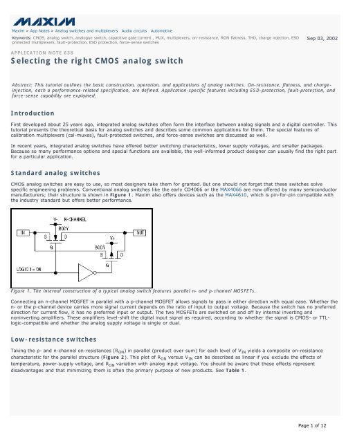
<strong>CMOS</strong> <strong>analog</strong> <strong>switch</strong>es are easy to use, so most designers take <strong>the</strong>m for granted. But one should not forget that <strong>the</strong>se <strong>switch</strong>es solve<br />
specific engineering problems. Conventional <strong>analog</strong> <strong>switch</strong>es like <strong>the</strong> early CD4066 or <strong>the</strong> MAX4066 are now offered by many semiconductor<br />
manufacturers; <strong>the</strong>ir structure is shown in Figure 1. Maxim also offers devices such as <strong>the</strong> MAX4610, which is pin-for-pin compatible with<br />
<strong>the</strong> industry standard but offers better performance.<br />
Figure 1. The internal construction of a typical <strong>analog</strong> <strong>switch</strong> features parallel n- and p-channel MOSFETs.<br />
Connecting an n-channel MOSFET in parallel with a p-channel MOSFET allows signals to pass in ei<strong>the</strong>r direction with equal ease. Whe<strong>the</strong>r <strong>the</strong><br />
n- or <strong>the</strong> p-channel device carries more signal current depends on <strong>the</strong> ratio of input to output voltage. Because <strong>the</strong> <strong>switch</strong> has no preferred<br />
direction for current flow, it has no preferred input or output. The two MOSFETs are <strong>switch</strong>ed on and off by internal inverting and<br />
noninverting amplifiers. These amplifiers level-shift <strong>the</strong> digital input signal as required, according to whe<strong>the</strong>r <strong>the</strong> signal is <strong>CMOS</strong>- or TTLlogic-compatible<br />
and whe<strong>the</strong>r <strong>the</strong> <strong>analog</strong> supply voltage is single or dual.<br />
Low-resistance <strong>switch</strong>es<br />
Taking <strong>the</strong> p- and n-channel on-resistances (R ON ) in parallel (product over sum) for each level of V IN yields a composite on-resistance<br />
characteristic for <strong>the</strong> parallel structure (Figure 2). This plot of R ON versus V IN can be described as linear if you exclude <strong>the</strong> effects of<br />
temperature, power-supply voltage, and R ON variation with <strong>analog</strong> input voltage. You should be aware that <strong>the</strong>se effects represent<br />
disadvantages and that minimizing <strong>the</strong>m is often <strong>the</strong> primary purpose of new products. See Table 1.<br />
Page 1 of 12
Figure 2. The n-channel and p-channel on-resistances of Figure 1 form a low-valued composite on-resistance.<br />
Page 2 of 12
Table 1. Low-resistance <strong>switch</strong>es<br />
Part Number<br />
MAX312/MAX313/MAX314<br />
MAX4614/MAX4615/MAX4616<br />
Function<br />
4 SPST<br />
NC/NO/NO,NC<br />
4 SPST<br />
NO/NC/NO,NC<br />
R DS(ON)<br />
(Ω<br />
max)<br />
I COM(OFF) /I D(OFF)<br />
(nA max)<br />
R ON<br />
Match<br />
(Ω<br />
max)<br />
R ON<br />
Flatness<br />
(Ω max<br />
t ON /t OFF<br />
(ns<br />
max)<br />
Charge<br />
Injection<br />
(pC typ)<br />
10 0.5 1.5 2 225/185 30<br />
10 1 1 1 12/10 6.5<br />
MAX4617 8X1 Mux 10 1 1 1 15/10 3<br />
MAX4618 Dual 4X1 Mux 10 1 1 - 15/10 3<br />
MAX4619 3 SPDT 10 1 1 - 15/10 3<br />
MAX4621 2 SPST NO 5 0.5 0.5 0.5 250/200 80<br />
MAX4622 2 SPDT 5 0.5 0.5 0.5 250/200 80<br />
MAX4623 2 DPST 5 0.5 0.5 0.5 250/200 80<br />
MAX4661/MAX4662/MAX4663<br />
MAX4664/MAX4665/MAX4666<br />
MAX4667/MAX4668/MAX4669<br />
4 SPST<br />
NO/NC/NO,NC<br />
4 SPST<br />
NO/NC/NO,NC<br />
2 SPST<br />
NO/NC/NO,NC<br />
2.5 0.5 - 0.4 250/200 120<br />
4 0.5 0.5 0.5 300/200 300<br />
2.5 0.5 0.4 0.4 300/200 450<br />
MAX4680/MAX4690/MAX4694 2 SPST NO 1.25 0.5 0.25 0.3 275/200 -60<br />
MAX4734 1 4:1 MUX 0.8 1 0.2 0.1 25/20 60<br />
MAX4741 2 SPST 0.8 1 0.08 0.18 24/16 28<br />
MAX4751 4 SPST NO 0.9 2.5 0.12 0.1 30/25 21<br />
MAX4756<br />
4 SPDT<br />
NO/NC<br />
0.85 3 0.35 0.4 150/40 50<br />
MAX4780 4 2:1 MUX 1 1 0.15 0.2 25/10 5<br />
MAX4781 1 8:1 MUX 1 2 0.4 0.2 25/15 40<br />
MAX4855<br />
2 SPST<br />
NO/NC<br />
1 2 0.12 0.27 60/40 170<br />
Supply<br />
Voltage<br />
Range<br />
(V)<br />
±4.5 to<br />
±20<br />
+2 to<br />
+5.5<br />
+2 to<br />
+5.5<br />
+2 to<br />
+5.5<br />
+2 to<br />
+5.5<br />
±4.5 to<br />
±20 or<br />
+4.5 to<br />
+36<br />
±4.5 to<br />
±20 or<br />
+4.5 to<br />
+36<br />
±4.5 to<br />
±20 or<br />
+4.5 to<br />
+36<br />
±4.5 to<br />
±20 or<br />
+4.5 to<br />
+36<br />
±4.5 to<br />
±20 or<br />
+4.5 to<br />
+36<br />
±4.5 to<br />
±20 or<br />
+4.5 to<br />
+36<br />
±4.5 to<br />
±20 or<br />
+4.5 to<br />
+36<br />
+1.6 to<br />
+3.6<br />
1.6 to<br />
+3.6<br />
+1.6 to<br />
+3.6<br />
+1.8 to<br />
+5.5<br />
+1.6 to<br />
+4.2<br />
+1.6 to<br />
+3.6<br />
+2 to<br />
+5.5<br />
Pin-<br />
Package<br />
16-DIP|SO<br />
14-DIP/SO/16-<br />
QSOP<br />
16-<br />
DIP/SO/QSOP<br />
16-<br />
DIP/SO|QSOP<br />
16-<br />
DIP|SO|6/QSOP<br />
16-DIP/SO<br />
16-DIP/SO<br />
16-DIP/SO<br />
16-<br />
DIP/SO|/SSOP<br />
16-DIP|/SO<br />
16-DIP/SO<br />
16-DIP/WID<br />
SO/SSOP<br />
10-µMAX®<br />
12-TQFN<br />
8-SOT23<br />
14-TSSOP<br />
16-QFN<br />
36-UCSP<br />
36-TQFN<br />
16-TQFN<br />
16-TSSOP<br />
16-QFN<br />
16-TSSOP<br />
16-TQFN<br />
16-TSSOP<br />
The first <strong>analog</strong> <strong>switch</strong>es operated on ±20V supply voltages and had several hundred ohms of R ON . Recent products (<strong>the</strong> MAX4601, for<br />
example) achieve 2.5Ω maximum R ON with a much lower supply voltage. Supply voltage has a substantial effect on R ON (Figure 3). The<br />
MAX4601 specifies signal and supply voltages from 4.5V to 36V or from ±4.5V to ±20V. As you can see, R ON increases for lower supply<br />
voltages. The max R ON is about 8Ω at 5V, 3Ω at 12V, and only 2.5Ω at 24V. Many new <strong>analog</strong> <strong>switch</strong>es specify low-voltage operation for<br />
supply voltages down to 2V. For 5V supplies, Figure 4 compares <strong>the</strong> Maxim <strong>switch</strong>es with older types.<br />
Page 3 of 12
Figure 3. Higher supply voltage causes lower on-resistance.<br />
Figure 4. At +5V supply voltage, later-generation <strong>analog</strong> <strong>switch</strong>es have lower on-resistance.<br />
When selecting <strong>switch</strong>es for single-supply systems, try to choose from those intended for single-supply use. Such devices save one pin,<br />
because <strong>the</strong>y do not require separate V- and ground pins. As a result, this economy of pins enables a single-pole/double-throw (SPDT)<br />
<strong>switch</strong> to fit into a miniscule 6-pin SOT23 package. Similarly, low-voltage dual-supply applications call for dual-supply <strong>switch</strong>es. These<br />
<strong>switch</strong>es require a V- pin in addition to <strong>the</strong> ground pin, and typically specify a logic interface with standard <strong>CMOS</strong> and TTL levels. The SPST<br />
MAX4529, for example, is also available in a 6-pin SOT23 package.<br />
Many high-performance <strong>analog</strong> systems still rely on higher-level bipolar supplies such as ±15V or ±12V. The interface to <strong>the</strong>se voltages<br />
requires an additional supply pin commonly labeled V L (shown in <strong>the</strong> MAX318 data sheet). The V L supply connects to <strong>the</strong> system logic<br />
voltage, which is usually 5V or 3.3V. Having <strong>the</strong> input logic signals referenced to <strong>the</strong> actual logic levels increases <strong>the</strong> noise margin and<br />
prevents excessive power dissipation.<br />
Often misunderstood is <strong>the</strong> <strong>analog</strong>-<strong>switch</strong> concept pertaining to input logic levels and <strong>the</strong>ir effect on supply current. If <strong>the</strong> logic inputs are at<br />
ground or V CC (or V L when available), <strong>analog</strong> <strong>switch</strong>es have essentially no supply current. Applying TTL levels to a 5V <strong>switch</strong>, however, can<br />
cause <strong>the</strong> supply current to increase more than 1000 times. To avoid unnecessary power consumption, you should avoid TTL levels, which<br />
are simply a legacy of <strong>the</strong> 1980s.<br />
Signal handling<br />
Figure 3 also shows <strong>the</strong> value of R ON versus signal voltage. These curves fall within <strong>the</strong> specified range of supply voltage, because <strong>analog</strong><br />
<strong>switch</strong>es can only handle <strong>analog</strong>-signal levels between <strong>the</strong> supply voltages. Under- or overvoltage inputs can permanently damage an<br />
Page 4 of 12
protected <strong>switch</strong> by producing uncontrolled currents through internal diode networks. Normally, <strong>the</strong>se diodes protect <strong>the</strong> <strong>switch</strong> against<br />
short-duration electrostatic discharge (ESD) as high as ±2kV.<br />
R ON for a typical <strong>CMOS</strong> <strong>analog</strong> <strong>switch</strong> causes a linear reduction of signal voltage that is proportional to current passing through <strong>the</strong> <strong>switch</strong>.<br />
This might not be a disadvantage for modest levels of current or if <strong>the</strong> design accounts for R ON effects. However, if you accept a certain level<br />
of R ON , <strong>the</strong>n channel matching and R ON flatness can interest you. Channel matching describes <strong>the</strong> variation of R ON for <strong>the</strong> channels of one<br />
device; R ON flatness describes <strong>the</strong> variation of R ON versus signal range for a single channel. Typical values for <strong>the</strong>se parameters are 2Ω to<br />
5Ω, and only 0.5Ω maximum for very low R ON <strong>switch</strong>es (MAX4601, for instance). The smaller <strong>the</strong> ratio of matching/R ON or flatness/R ON is,<br />
<strong>the</strong> more accurate <strong>the</strong> <strong>switch</strong>.<br />
In most applications, you can avoid excessive <strong>switch</strong> current by modifying <strong>the</strong> circuit design. To change <strong>the</strong> gain of an op amp by <strong>switch</strong>ing<br />
between different feedback resistances, for example, choose a configuration that places <strong>the</strong> <strong>switch</strong> in series with a high-impedance input<br />
(Figure 5a). Because <strong>switch</strong> currents are insignificant, you can ignore <strong>the</strong> value of R ON and its temperature coefficient. Switch current in <strong>the</strong><br />
alternative design (Figure 5b) can be substantial, because it depends on <strong>the</strong> output voltage.<br />
Figure 5. Gain-control circuits are good (a) or bad (b) depending on <strong>the</strong> amount of current through <strong>the</strong> <strong>switch</strong>.<br />
Break-before-make<br />
Turn-on and turn-off times (t ON and t OFF ) for most <strong>analog</strong> <strong>switch</strong>es vary from below 60ns to as high as 1µs. For Maxim's "clickless" audio<br />
<strong>switch</strong>es, t ON and t OFF are in <strong>the</strong> millisecond range to eliminate <strong>the</strong> audible clicks o<strong>the</strong>rwise present when <strong>switch</strong>ing audio signals. The<br />
relative magnitudes are also important: t ON > t OFF yields break-before-make action, and t OFF > t ON yields make-before-break. This<br />
distinction is critical for some applications.<br />
Figure 5a shows that you must take care in <strong>switch</strong>ing between <strong>the</strong> two gains. One <strong>switch</strong> is normally closed in a typical make-before-break<br />
application. In changing gain you must avoid opening both <strong>switch</strong>es at once; that is, <strong>the</strong> second <strong>switch</strong> must close before <strong>the</strong> first <strong>switch</strong><br />
opens. O<strong>the</strong>rwise, <strong>the</strong> op amp applies open-loop gain and drives its output to <strong>the</strong> rails. The opposite configuration (break-before-make) is<br />
also useful in <strong>switch</strong>ing among different input signals to a single op amp. To avoid short circuits between <strong>the</strong> input channels, a given<br />
connection must be <strong>switch</strong>ed off before <strong>the</strong> next one is <strong>switch</strong>ed on.<br />
When a changing signal level modulates <strong>the</strong> on-resistance, causing a variation in <strong>the</strong> insertion loss, <strong>analog</strong> <strong>switch</strong>es generate total harmonic<br />
distortion (THD). Consider a 100Ω <strong>switch</strong> with 10Ω R ON flatness, for example. Loading this <strong>switch</strong> with a 600Ω termination produces 0.24%<br />
of THD. Consequently, for low THD you should avoid loading <strong>the</strong> output of an <strong>analog</strong> <strong>switch</strong>.<br />
Charge-injection effects<br />
As mentioned above, low R ON is not necessary in all applications. Lower R ON requires greater chip area. The result is a greater input<br />
capacitance whose charge and discharge currents dissipate more power in every <strong>switch</strong>ing cycle. Based on <strong>the</strong> time constant t = RC, this<br />
charging time depends on load resistance (R) and capacitance (C). It normally lasts a few tens of nanoseconds, but low-R ON <strong>switch</strong>es have<br />
longer-duration on and off periods. High-R ON <strong>switch</strong>es are faster.<br />
Maxim offers both types of <strong>switch</strong>es, each with <strong>the</strong> same pinout in <strong>the</strong> same miniature SOT23 package. The MAX4501 and <strong>the</strong> MAX4502<br />
specify higher on-resistance but shorter on/off times. The MAX4514 and <strong>the</strong> MAX4515 have lower on-resistance but longer <strong>switch</strong>ing times.<br />
Page 5 of 12
Ano<strong>the</strong>r negative consequence of low on-resistance can be <strong>the</strong> higher charge injection caused by higher levels of capacitive gate current. A<br />
certain amount of charge is added to or subtracted from <strong>the</strong> <strong>analog</strong> channel with every on or off transition of <strong>the</strong> <strong>switch</strong> (Figure 6). For<br />
<strong>switch</strong>es connected to high-impedance outputs, this action can cause significant changes in <strong>the</strong> expected output signal. A small parasitic<br />
capacitor (C L ) with no o<strong>the</strong>r load adds a variation of ΔV OUT , so charge injection can be calculated as Q = ΔV OUT C L .<br />
Figure 6. Charge injection from <strong>the</strong> <strong>switch</strong>-control signal causes a voltage error at <strong>the</strong> <strong>analog</strong> output.<br />
A track/hold amplifier, which maintains a constant <strong>analog</strong> output during conversion by an A/D converter, offers a good example of this<br />
(Figure 7). Closing S1 charges <strong>the</strong> small buffer capacitor (C) to <strong>the</strong> input voltage (V S ). The value of C is only a few picofarads, and V S<br />
remains stored on C when S1 opens. The held voltage (V H ) is applied to <strong>the</strong> buffer by closing S2 at <strong>the</strong> beginning of a conversion. The highimpedance<br />
buffer <strong>the</strong>n maintains V H constant over <strong>the</strong> ADC's conversion time. For short acquisition times, <strong>the</strong> track/hold's capacitor must be<br />
small and S1's on-resistance must be low. On <strong>the</strong> o<strong>the</strong>r hand, charge injection can cause V H to change by ±ΔV OUT (a few millivolts),<br />
<strong>the</strong>reby affecting <strong>the</strong> accuracy of <strong>the</strong> following ADC.<br />
Figure 7. A typical track/hold function requires precise control of <strong>the</strong> <strong>analog</strong> <strong>switch</strong>es.<br />
Having reviewed <strong>the</strong>se fundamentals, we now focus on innovative <strong>switch</strong>es for special applications.<br />
T-<strong>switch</strong>es for higher frequencies<br />
The T-<strong>switch</strong> is suitable for video and o<strong>the</strong>r frequencies above 10MHz. It consists of two <strong>analog</strong> <strong>switch</strong>es in series, with a third <strong>switch</strong><br />
connected between ground and <strong>the</strong>ir joining node. This arrangement provides higher off-isolation than a single <strong>switch</strong>. The capacitive<br />
crosstalk for a T-<strong>switch</strong> turned off typically rises with frequency due to <strong>the</strong> parasitic capacitances in parallel with each of <strong>the</strong> series <strong>switch</strong>es<br />
(Figure 8). The problem in operating a high-frequency <strong>switch</strong> does not lie in turning it on, but in turning it off.<br />
When <strong>the</strong> T-<strong>switch</strong> is turned on, S1 and S3 are closed and S2 is open. In <strong>the</strong> off state, S1 and S3 are open and S2 is closed. In that case<br />
(<strong>the</strong> off state) <strong>the</strong> signal tries to couple through <strong>the</strong> off-capacitance of <strong>the</strong> series MOSFETs, but is shunted to ground by S3. If you compare<br />
<strong>the</strong> off isolation at 10MHz for a video T-<strong>switch</strong> (MAX4545) and a standard <strong>analog</strong> <strong>switch</strong> (MAX312), <strong>the</strong> result is dramatic: -80dB versus -<br />
36dB for <strong>the</strong> standard <strong>switch</strong>.<br />
Page 6 of 12
Figure 8. The T-<strong>switch</strong> configuration attenuates RF frequencies that couple through <strong>the</strong> stray capacitance between <strong>the</strong> source and <strong>the</strong> drain<br />
of an open (off) <strong>switch</strong>.<br />
Smaller packages<br />
O<strong>the</strong>r advantages for <strong>CMOS</strong> <strong>analog</strong> <strong>switch</strong>es include small packages, such as <strong>the</strong> 6-pin SOT23, and no mechanical parts (unlike reed relays).<br />
Maxim offers a small video <strong>switch</strong> (MAX4529) as well as a standard, low-voltage SPDT <strong>switch</strong> (MAX4544). Both come in 6-pin SOT23<br />
packages and operate from supply voltages in <strong>the</strong> 2.7V to 12V range. The MAX4544 is <strong>the</strong> smallest SPDT <strong>analog</strong> <strong>switch</strong> currently available.<br />
See Table 2.<br />
Table 2. Small packages<br />
Part Number<br />
MAX4501/MAX4502<br />
MAX4503/MAX4504<br />
MAX4514/MAX4515<br />
MAX4516/MAX4517<br />
Function<br />
SPST<br />
NO/NC<br />
SPST<br />
NO/NC<br />
SPST<br />
NO/NC<br />
SPST<br />
NO/NC<br />
R DS(ON)<br />
(Ω<br />
max)<br />
I COM(OFF)<br />
/I D(OFF)<br />
(nA<br />
max)<br />
R ON<br />
Flatness<br />
(Ω<br />
max)<br />
t ON /t OFF<br />
(ns<br />
max)<br />
Charge<br />
Injection<br />
(pC max)<br />
Off-Isolation (dB<br />
max)/Frequency<br />
(MHz)<br />
Supply<br />
Voltage<br />
Range (V)<br />
250 1 - 75/50 10 -100/0.1 +2 to +12<br />
250 1 - 150/100 10 -90/0.1 ±1 to ±6<br />
20 1 3 150/100 10 -90/0.1 +2 to +12<br />
20 1 4 100/150 20 -86/0.1 ±1 to ±6<br />
MAX4529 SPST NC 70 1 10 75/75 10 -80/10<br />
±2.7 to ±6 or<br />
+2.7 to +12<br />
Pin-<br />
Package<br />
5-SOT23-5|8-<br />
DIP/SO<br />
5-SOT23-5|8-<br />
DIP/SO<br />
5-SOT23-5|8-<br />
DIP/SO<br />
5-/SOT23-<br />
5|8-DIP/SO<br />
6-SOT23-6|8-<br />
DIP/SO//<br />
µMAX<br />
MAX4544 SPDT 60 0.1 6 100/75 5 -76/-90 +2.7 to +12 6-SOT23-6|8-<br />
DIP/SO/µMAX<br />
MAX4707<br />
1 SPDT<br />
NO<br />
3 1 0.85 20/15 5 -82/1 +1.8 to +5.5<br />
MAX4719 2 SPDT 20 0.5 1.2 80/40 18 -80/1 +1.8 to +5.5<br />
MAX4723<br />
2 SPDT<br />
NO/NC<br />
4.5 0.5 1.2 80/40 18 -80/1 +1.8 to +5.5<br />
5-SC70<br />
6-SC70<br />
10-µMAX<br />
12-USCP<br />
8-µMAX<br />
9-USCP<br />
MAX4730 1 SPDT 5.5 - 0.95 45/26 3 -67/1 +1.8 to +5.5 6-SC70<br />
MAX4733<br />
2 SPDT<br />
NO/NC<br />
50 0.1 9 150/60 7.5 -72/1 +2 to +11<br />
8-µMAX<br />
9-/USCP<br />
As mentioned earlier, Maxim offers many variations of popular <strong>analog</strong> <strong>switch</strong>es like <strong>the</strong> CD4066, including a family of low-cost quad <strong>analog</strong><br />
<strong>switch</strong>es (MAX4610–MAX4612). The MAX4610 is a pin-compatible improvement over <strong>the</strong> industry-standard 4066, but with lower supply<br />
voltage (as low as 2V) and higher accuracy: channel matching to within 4Ω maximum and channel flatness to within 18Ω maximum. This<br />
family of parts offers three <strong>switch</strong> configurations, and <strong>the</strong>ir lower on-resistance (< 100Ω at 5V) suits low-voltage applications. A tiny 14-pin<br />
TSSOP package (6.5 x 5.1 x 1.1mm ³ max) solves <strong>the</strong> problem of board space.<br />
Page 7 of 12
ESD-protected <strong>switch</strong>es<br />
Based on <strong>the</strong> success of Maxim's ESD-protected interface products, ±15kV ESD protection was added to some of <strong>the</strong> more recent <strong>analog</strong><br />
<strong>switch</strong>es (Table 3). Maxim now offers <strong>the</strong> first <strong>switch</strong>es with ±15kV ESD protection per IEC 1000-4-2 Level 4 (<strong>the</strong> highest level). All <strong>analog</strong><br />
inputs are ESD-tested using <strong>the</strong> Human Body Model, as well as <strong>the</strong> Contact and Air-Gap Discharge methods specified in IEC 1000-4-2. The<br />
MAX4551/MAX4552/MAX4553 <strong>switch</strong>es are pin-compatible with many standard quad-<strong>switch</strong> families such as <strong>the</strong> DG201/211 and <strong>the</strong> MAX391<br />
types. To augment standard multiplexer families like <strong>the</strong> 74HC4051 and <strong>the</strong> MAX4581, Maxim also released ESD-protected multiplexers. You<br />
no longer need to use costly TransZorbs® to protect your <strong>analog</strong> inputs.<br />
Table 3. ±15k ESD per IEC 1000-4-2, in 16-pin DIP, SO, and QSOP packages<br />
Part<br />
Number<br />
Function R DS(ON)<br />
(Ω<br />
max)<br />
I COM(OFF)<br />
/I D(OFF)<br />
(nA<br />
max)<br />
R ON<br />
Match<br />
(Ω<br />
max)<br />
R ON<br />
Flatness<br />
(Ω<br />
max)<br />
t ON /t OFF<br />
(ns max)<br />
Charge<br />
Injection (pC<br />
typ)<br />
100kHz OFF-<br />
Isolation/Crosstalk (dB<br />
typ)<br />
Supply Voltage<br />
Range (V)<br />
MAX4551<br />
MAX4552<br />
MAX4553<br />
4 SPST<br />
NO<br />
4 SPST<br />
NC<br />
4 SPST<br />
NO, NC<br />
120 ±1 4 8 110/90 2 -90/-90<br />
120 ±1 4 8 110/90 2 -90/-90<br />
120 ±1 4 8 110/90 2 -90/-90<br />
MAX4558 8 x 1 Mux 160 ±1 6 8 150/120 2.4 -96/-93<br />
MAX4559<br />
Dual 4 x<br />
1 Mux<br />
160 ±1 6 8 150/120 2.4 -96/-93<br />
MAX4560 3 SPDT 160 ±1 6 8 150/120 2.4 -96/-93<br />
MAX4569<br />
1 SPST<br />
NO<br />
70 ±0.5 2 4 150/80 6 -75<br />
MAX4577 2 SPST 70 ±0.5 2 4 150/80 4 -75/90<br />
MAX4620<br />
4 SPST<br />
NO<br />
70 ±0.5 2 4 150/80 5 -75/90<br />
±2 to ±6 or +2<br />
to +12<br />
±2 to ±6 or +2<br />
to +12<br />
±2 to ±6 or +2<br />
to +12<br />
±2 to ±6 or +2<br />
to +12<br />
±2 to ±6 or +2<br />
to +12<br />
±2 to ±6 or +2<br />
to +12<br />
±2 to ±6<br />
+2 to +12<br />
±2 to ±6<br />
+2 to +12<br />
±2 to ±6<br />
+2 to +12<br />
Fault-protected <strong>switch</strong>es<br />
As mentioned under "Signal Handling" above, <strong>the</strong> supply-voltage rails for an <strong>analog</strong> <strong>switch</strong> restrict <strong>the</strong> allowed range for input signal<br />
voltage. Normally this restriction is not a problem, but in some cases <strong>the</strong> supply voltage can be turned off with <strong>analog</strong> signals still present.<br />
That condition can permanently damage <strong>the</strong> <strong>switch</strong>, as can transients outside <strong>the</strong> normal range of <strong>the</strong> power supply. Maxim's fault-protected<br />
<strong>switch</strong>es and multiplexers guarantee overvoltage protection of ±25V and power-down protection of ±40V, along with rail-to-rail signal<br />
handling and <strong>the</strong> low on-resistance of a normal <strong>switch</strong> (Figure 9). The input pin, moreover, assumes a high impedance during fault<br />
conditions regardless of <strong>the</strong> <strong>switch</strong> state or load resistance. Only nanoamperes of leakage current can flow from <strong>the</strong> source.<br />
Figure 9. This internal structure shows <strong>the</strong> special circuitry in a fault-protected <strong>analog</strong> <strong>switch</strong>.<br />
If <strong>the</strong> <strong>switch</strong> (P2 or N2) is on, <strong>the</strong> COM output is clamped to <strong>the</strong> supply by two internal 'booster' FETs. Thus, <strong>the</strong> COM output remains within<br />
<strong>the</strong> supply rails and delivers a maximum of ±13mA depending on <strong>the</strong> load, but without a significant current at <strong>the</strong> NO/NC pin. The faultprotected<br />
<strong>switch</strong>es, MAX4511/MAX4512/MAX4513, are pin-compatible with <strong>the</strong> DG411–DG413 and DG201/DG202/DG213 types (Table 4).<br />
Note that signals pass equally well in ei<strong>the</strong>r direction through an ESD- and fault-protected <strong>switch</strong>, but <strong>the</strong>se protections apply only to <strong>the</strong><br />
input side.<br />
Page 8 of 12
Table 4. Fault protection with rail-to-rail signal swings<br />
Part<br />
Number<br />
MAX4505<br />
MAX4506<br />
MAX4507<br />
Function<br />
1 Line<br />
Protector<br />
3 Line<br />
Protector<br />
8 Line<br />
Protector<br />
R DS(ON)<br />
(Ω<br />
max)<br />
I COM(OFF)<br />
/I D(OFF)<br />
(nA<br />
MAX)<br />
R ON<br />
Match<br />
(Ω<br />
max)<br />
t ON /t OFF<br />
(ns<br />
max)<br />
Overvoltage<br />
Supplies<br />
ON/OFF (V)<br />
Charge<br />
Injection<br />
(pC max)<br />
100 ±0.5 - - ±36/±40 -<br />
100 ±0.5 7 - ±36/±40 -<br />
100 ±0.5 7 - ±36/±40 -<br />
MAX4508 8 x 1 Mux 400 ±0.5 15 275/200 ±25/±40 10<br />
MAX4509 4 x 1 Mux 400 ±0.5 15 275/200 ±25/±40 10<br />
MAX4511 4 SPST NO 160 ±0.5 6 500/400 ±36/±40 5<br />
MAX4512 4 SPST NC 160 ±0.5 6 500/400 ±36/±40 5<br />
MAX4513<br />
4 SPST NO,<br />
NC<br />
160 ±0.5 6 500/400 ±36/±40 5<br />
MAX4533 4 SPDT 175 ±0.5 6 250/150 ±25/±40 5<br />
MAX4631 2 SPST NO 85 ±0.5 6 150/100 ±36/±40 10<br />
MAX4632 2 SPDT 85 ±0.5 6 150/100 ±25/±40 10<br />
MAX4633 2 DPST NO 85 ±0.5 6 150/100 ±36/±40 10<br />
MAX4510 1 SPST NC 160 ±0.5 - 500/175 ±36/±40 5<br />
MAX4520 2 SPDT NO 160 ±0.5 - 500/175 ±36/±40 5<br />
MAX4534 1 2:1MUX 275 ±2 10 275/200 ±25/±40 10<br />
MAX4535 2 2:1MUX 275 ±2 10 275/200 ±25/±40 10<br />
MAX4711 4 SPST NC 25 ±0.5 1 125/80 ±7/±12 25<br />
Supply Voltage<br />
Range(V)<br />
±8 to ±18 or +9<br />
to +36<br />
±8 to ±18 or +9<br />
to +36<br />
±8 to ±18 or +9<br />
to +36<br />
±4.5 to ±20 or +9<br />
to +36<br />
±4.5 to ±20 or +9<br />
to +36<br />
±8 to ±18 or +9<br />
to +36<br />
±8 to ±18 or +9<br />
to +36<br />
±8 to ±18 or +9<br />
to +36<br />
±4.5 to ±20 or +9<br />
to +36<br />
±4.5 to ±20 or +9<br />
to +36<br />
±4.5 to ±20 or +9<br />
to +36<br />
±4.5 to ±20 or +9<br />
to +36<br />
+9 to +36<br />
±4.5 to ±20<br />
+9 to +36<br />
±4.5 to ±20<br />
+9 to +36<br />
±4.5 to ±20<br />
+9 to +36<br />
±4.5 to ±20<br />
+2.7 to +11<br />
±2.7 to ±5.5<br />
Pin-<br />
Package<br />
5-SOT|8-µMAX<br />
8-DIP/SO/CERDIP<br />
18-/DIP/SO/20-SSOP<br />
16-DIP/SO<br />
16-DIP/SO<br />
16-DIP/SO/CERDIP<br />
16/-<br />
DIP|16/SO|16/CERDIP<br />
16-DIP/SO/CERDIP<br />
20-Wide SO/SSOP<br />
16-DIP/SO/CERDIP<br />
16-DIP/SO/CERDIP<br />
16-DIP/SO/CERDIP<br />
6-/SOT23<br />
8-µMAX<br />
6-SOT23<br />
8-µMAX<br />
14-TSSOP/SO/DIP<br />
14-TSSOP/SO/DIP<br />
8-µMAX<br />
9-UCSP<br />
Force-sense <strong>switch</strong>es<br />
Maxim offers a family of <strong>analog</strong> <strong>switch</strong>es with different <strong>switch</strong> types residing in <strong>the</strong> same package. The MAX4554/MAX4555/MAX4556<br />
devices, for instance, are configured as force-sense <strong>switch</strong>es for Kelvin sensing in automated test equipment (ATE). Each part contains lowresistance<br />
high-current <strong>switch</strong>es for forcing current and higher-resistance <strong>switch</strong>es for sensing voltage or <strong>switch</strong>ing guard signals. Onresistance<br />
for <strong>the</strong> current <strong>switch</strong>es is only 6Ω, and for <strong>the</strong> sensing <strong>switch</strong>es is 60Ω at ±15V supply voltages. The MAX4556 contains three<br />
SPDT <strong>switch</strong>es with break-before-make action.<br />
Typical force-sense applications are found in high-accuracy systems and in measurement systems that involve long distances (Figure 10).<br />
For 4-wire measurements, two wires force a voltage or current to <strong>the</strong> load, and two o<strong>the</strong>r wires connected directly to <strong>the</strong> load sense <strong>the</strong><br />
load voltage.<br />
Page 9 of 12
Figure 10. With <strong>the</strong> 4-wire technique, two wires force and two o<strong>the</strong>r wires sense <strong>the</strong> measured voltage.<br />
Alternatively, a 2-wire system senses load voltage at <strong>the</strong> ends of <strong>the</strong> force wires opposite <strong>the</strong> load. Load voltage is lower than <strong>the</strong> source<br />
voltage, because <strong>the</strong> forcing voltage or current causes a voltage drop along <strong>the</strong> wires. Longer distance between source and load, larger load<br />
current, and higher conductor resistance all contribute for this degradation. The resulting signal reduction can be overcome by using a 4-<br />
wire technique in which <strong>the</strong> two additional voltage-sensing conductors carry negligible current.<br />
Force-sense <strong>switch</strong>es simplify many applications, such as <strong>switch</strong>ing between one source and two loads in a 4-wire system. They are suitable<br />
for use in high-accuracy measurement systems, such as nanovoltmeters and femtoammeters, and for 8- or 12-wire force-and-sense<br />
measurements using <strong>the</strong> guard wires of triax cables. For more information, please see <strong>the</strong> MAX4554/MAX4555/MAX4556 data sheet.<br />
Multiplexers<br />
In addition to <strong>switch</strong>es, Maxim makes a number of multiplexers (muxes). A mux is a special version of a <strong>switch</strong> in which two or more inputs<br />
are selectively connected to a single output. A mux can be as simple as an SPDT <strong>switch</strong> or come in 4:1, 8:1, 16:1, or even dual 4:1 and 8:1<br />
combinations. The digital control for <strong>the</strong>se higher order muxes is similar to a binary decoder with three digital inputs required to select <strong>the</strong><br />
appropriate channel.<br />
A demultiplexer is basically a mux used backwards. That is, one input connects to two or more outputs based on <strong>the</strong> decoded address data.<br />
There are, finally, cross-point <strong>switch</strong>es. A cross-point <strong>switch</strong> is usually an M x N device, whereby any or all of M inputs may be connected to<br />
any or all of N outputs (and vice versa).<br />
Calibration multiplexers<br />
Calibration multiplexers (cal-muxes) are used in precision ADCs and o<strong>the</strong>r self-monitoring systems. They combine different components in<br />
one package: <strong>analog</strong> <strong>switch</strong>es for generating accurate voltage ratios from an input reference voltage; internal precision resistor-dividers;<br />
and a multiplexer for selecting between different inputs. Maxim introduced this combination of functions in a single package.<br />
Two of <strong>the</strong>se devices (MAX4539 and MAX4540) can balance two major errors associated with an ADC system: offset and gain error. Using<br />
<strong>the</strong> internal precision voltage-dividers, <strong>the</strong>se devices measure gain and offset in a few steps, controlled trough <strong>the</strong> serial interface of a<br />
microcontroller. The reference ratios 15/4096 and 4081/4096 (with respect to <strong>the</strong> external reference voltage) are accurate to 15 bits. The<br />
ratios (5/8)(V+ - V-) and V+/2 are accurate to 8 bits.<br />
The cal-mux first applies one-half <strong>the</strong> supply voltage to verify that power is present. The system <strong>the</strong>n measures zero offset and gain error,<br />
and forms an equation to correct <strong>the</strong> subsequent readings. Zero input voltage, for example, should produce a digital zero output. The calmux<br />
calibrates for offset error by applying a very small input voltage of 15/4096 referred to (V EFHI - REFLO ). For a 12-bit ADC with 4.096V<br />
reference, 15/4096 equals 15mV and also 15 LSBs. The digital output <strong>the</strong>refore should be binary 000000001111. To measure offset error,<br />
<strong>the</strong> microcontroller simply records <strong>the</strong> difference between binary 000000001111 and <strong>the</strong> ADC's actual output.<br />
To measure gain error, <strong>the</strong> cal-mux applies a voltage of 4081/4096 referred to (V REFHI - V REFLO ). The microcontroller <strong>the</strong>n records <strong>the</strong><br />
difference between binary 111111110000 and <strong>the</strong> ADC's digital output. Knowing <strong>the</strong> ADC's offset and gain error, <strong>the</strong> system software<br />
constructs calibration factors that adjust <strong>the</strong> subsequent outputs to produce correct readings. The cal-mux <strong>the</strong>n serves as a conventional<br />
multiplexer, but with <strong>the</strong> ability to recalibrate <strong>the</strong> system periodically.<br />
Page 10 of 12
USB 2.0 <strong>switch</strong>es<br />
A universal serial bus (USB) is a high-speed interface for handheld devices to communicate with computers. Multiple USB devices can be<br />
connected to a computer, and <strong>analog</strong> <strong>switch</strong>es are used to route <strong>the</strong> USB signal to different devices. The USB 2.0 is a high-speed signal<br />
that requires a high-bandwidth and low-capacitance <strong>analog</strong> <strong>switch</strong>.<br />
Maxim offers a good selection of USB 2.0-compliant <strong>switch</strong>es ideal for USB 2.0 high-speed applications. Table 5 shows a few examples of<br />
USB 2.0 <strong>switch</strong>es.<br />
Table 5. USB 2.0 <strong>switch</strong>es<br />
Part<br />
Functions R ON (O,<br />
max)<br />
R ON Match<br />
(O, max)<br />
t ON /t OFF<br />
(ns, max)<br />
I COM(OFF)<br />
(nA, max)<br />
C ON<br />
(pF,<br />
typ)<br />
C OFF<br />
(pF,<br />
typ)<br />
Charge<br />
Injection<br />
(pC)<br />
BW<br />
(MHz)<br />
Supply Voltage<br />
Range (V)<br />
MAX4906F 2 SPDT 7 1.2 60/30 1000 6 2 5 1000 3.0 to 3.6<br />
MAX4907F<br />
2 SPST<br />
NO<br />
7 1.2 60/30 1000 4 2 5 1000 3.0 to 3.6<br />
MAX4906EF 2 SPDT 7 0.8 1.4/35 1000 10 9 20 500 2.7 to 3.6<br />
MAX4899E 3 x 1 MUX 5 0.8 — 1000 15 10.2 25 425 2.7 to 3.6<br />
MAX4899AE 4 x 1 MUX 5 0.8 — 1000 15 10.5 25 425 2.7 to 3.6<br />
High-voltage <strong>switch</strong>es<br />
In ultrasound applications, high-voltage pulses (±100V) are applied to transducers to generate ultrasonic waves. Analog <strong>switch</strong>es are<br />
required for routing <strong>the</strong>se high-voltage signals between <strong>the</strong> transducers and <strong>the</strong> main systems, so <strong>the</strong> <strong>switch</strong>es must be able to handle highvoltage<br />
signals.<br />
Maxim offers a good selection of high-voltage <strong>analog</strong> <strong>switch</strong>es that are ideal for ultrasound medical applications. Table 6 shows a few<br />
examples.<br />
Table 6. High-voltage <strong>switch</strong>es<br />
Part<br />
MAX4800A/MAX4802A<br />
MAX14800–<br />
MAX14803<br />
Functions<br />
8 SPST<br />
NO<br />
16 SPST<br />
NO<br />
V SUPPLY<br />
(Single, V)<br />
V SUPPLY<br />
(Single, V)<br />
V SUPPLY<br />
(Dual, ±V)<br />
V SUPPLY<br />
(Dual, ±V)<br />
min max min max<br />
BW<br />
(MHz)<br />
I L(OFF)<br />
(nA)<br />
t ON<br />
(ns)<br />
t OFF<br />
(ns)<br />
C ON<br />
(pF)<br />
40 200 40 100 20 2000 5000 5000 36 11<br />
40 200 40 100 20 2000 3500 3500 36 11<br />
C OFF<br />
(pF)<br />
µMAX is a registered trademark of Maxim Integrated Products, Inc.<br />
TransZorb is a registered trademark of Vishay Intertechnology, Inc.<br />
UCSP is a trademark of Maxim Integrated Products, Inc.<br />
Related Parts<br />
MAX4066 Low-Cost, Low-Voltage, Quad, SPST, <strong>CMOS</strong> Analog Switch -- Free Samples<br />
MAX4514 Low-Voltage, Low-On-Resistance, SPST, <strong>CMOS</strong> Analog Switches -- Free Samples<br />
MAX4515 Low-Voltage, Low-On-Resistance, SPST, <strong>CMOS</strong> Analog Switches -- Free Samples<br />
MAX4529 Low-Voltage, Bidirectional RF Video Switch<br />
-- Free Samples<br />
MAX4545 Quad/Dual, Low-Voltage, Bidirectional RF Video Switches -- Free Samples<br />
MAX4601 2.5Ω, Quad, SPST, <strong>CMOS</strong> Analog Switches<br />
-- Free Samples<br />
MAX4610 Low-Voltage, Quad, SPST <strong>CMOS</strong> Analog Switches<br />
-- Free Samples<br />
Automatic Updates<br />
Would you like to be automatically notified when new application notes are published in your areas of interest? Sign up for EE-Mail.<br />
Application note 638: www.maxim-ic.com/an638<br />
More Information<br />
For technical support: www.maxim-ic.com/support<br />
For samples: www.maxim-ic.com/samples<br />
O<strong>the</strong>r questions and comments: www.maxim-ic.com/contact<br />
Page 11 of 12
<strong>AN638</strong>, AN 638, APP638, Appnote638, Appnote 638<br />
Copy<strong>right</strong> © by Maxim Integrated Products<br />
Additional legal notices: www.maxim-ic.com/legal<br />
Page 12 of 12