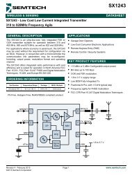
XE1203F - Semtech
XE1203F - Semtech
XE1203F - Semtech

You also want an ePaper? Increase the reach of your titles
YUMPU automatically turns print PDFs into web optimized ePapers that Google loves.
<strong>XE1203F</strong><br />
<strong>XE1203F</strong><br />
433 MHz / 868 MHz / 915 MHz<br />
Low-Power, Integrated UHF Transceiver<br />
GENERAL DESCRIPTION<br />
The <strong>XE1203F</strong> is a single chip transceiver operating<br />
in the 433, 868 and 915 MHz license-free ISM<br />
(Industry Scientific and Medical) frequency bands. Its<br />
highly integrated architecture allows for minimum<br />
external components while maintaining design<br />
flexibility. All major RF communication parameters<br />
are programmable and most of them can be<br />
dynamically set. The <strong>XE1203F</strong> offers the excellent<br />
advantage of high data rate communication at rates<br />
of up to 152.3 kbit/s, without the need to modify the<br />
number or parameters of the external components.<br />
The <strong>XE1203F</strong> is optimized for low power<br />
consumption while offering high RF output power and<br />
exceptional receiver sensitivity. The device is suitable<br />
for applications which have to satisfy either the<br />
European (ETSI-300-220) or the North American<br />
(FCC part 15) regulatory standards. TrueRF<br />
technology enables a low –cost external component<br />
count (elimination of the SAW filter) whilst still<br />
satisfying ETSI and FCC regulations.<br />
APPLICATIONS<br />
• Automated Meter Reading (AMR)<br />
• Home Automation and Access Control<br />
• High-Quality Speech, Music and Data over RF<br />
• Applications requiring Konnex-compatibility<br />
KEY PRODUCT FEATURES<br />
• RF output power: up to +15 dBm<br />
• High reception sensitivity: down to –114 dBm<br />
(typical)<br />
• Low power consumption:<br />
R X = 14 mA; T X = 62 mA @15 dBm (typical)<br />
• Supply voltage down to 2.4V<br />
• Data rate from 1.2 to 152.3 kbit/s, NRZ coding<br />
• Konnex-compatible operation mode<br />
• 11-bit Barker encoder/decoder<br />
• On-chip frequency synthesizer with minimum<br />
frequency resolution of 500 Hz<br />
Continuous phase 2-level FSK modulation<br />
Received data pattern recognition<br />
• Bit-Synchronizer for incoming data/clock<br />
synchronization and recovery<br />
• RSSI (Received Signal Strength Indicator)<br />
• FEI (Frequency Error Indicator)<br />
• RoHS green package<br />
ORDERING INFORMATION<br />
Part number Temperature Package<br />
range<br />
<strong>XE1203F</strong>I063TRLF -40 °C to +85 °C MLPQ48<br />
Rev 2 December 2008<br />
1<br />
www.semtech.com
<strong>XE1203F</strong><br />
Table of Contents<br />
1 Functional Block Diagram.................................................................................................................. 3<br />
2 Pin description .................................................................................................................................... 4<br />
3 Electrical Characteristics................................................................................................................... 5<br />
3.1 Absolute Maximum Operating Ranges ................................................................................................. 5<br />
3.2 Specifications........................................................................................................................................ 5<br />
3.2.1 Operating Range................................................................................................................................... 5<br />
3.2.2 Electrical Specifications ........................................................................................................................ 5<br />
4 GENERAL DESCRIPTION................................................................................................................... 7<br />
4.1 The Receiver Section............................................................................................................................ 7<br />
4.1.1 LNA & Receiver modes......................................................................................................................... 8<br />
4.1.2 Demodulation chain .............................................................................................................................. 8<br />
4.1.3 Demodulator.......................................................................................................................................... 8<br />
4.1.4 Bit synchronizer .................................................................................................................................... 9<br />
4.1.5 The DATA and DATAIN pins .............................................................................................................. 10<br />
4.1.6 Pattern recognition block .................................................................................................................... 10<br />
4.1.7 RSSI.................................................................................................................................................... 10<br />
4.1.8 Frequency Error Indicator – FEI ......................................................................................................... 12<br />
4.2 The Transmitter Section...................................................................................................................... 13<br />
4.2.1 Transmitter.......................................................................................................................................... 13<br />
4.2.2 Barker encoder/decoder ..................................................................................................................... 15<br />
4.3 The Frequency Synthesizer................................................................................................................ 16<br />
4.3.1 Clock Output for external processor ................................................................................................... 17<br />
5 SERIAL Interface definition AND Principles of operation ............................................................ 18<br />
5.1 Serial Control Interface ....................................................................................................................... 18<br />
5.2 Configuration and Status registers ..................................................................................................... 20<br />
5.2.1 The ConfigSwitch Register ................................................................................................................. 20<br />
5.2.2 RTParam Configuration Register........................................................................................................ 22<br />
5.2.3 FSParam Configuration Register........................................................................................................ 23<br />
5.2.4 SWParam Configuration Register - switching parameters ................................................................. 24<br />
5.2.5 DataOut Status Register ..................................................................................................................... 25<br />
5.2.6 ADParam Configuration Register ....................................................................................................... 25<br />
5.2.7 Pattern register ................................................................................................................................... 27<br />
5.2.8 Test Registers and additional settings................................................................................................ 28<br />
5.3 Operating Modes ................................................................................................................................ 28<br />
5.3.1 Standard power up sequence for the receiver and transmitter .......................................................... 28<br />
5.4 Selection of the reference frequency .................................................................................................. 29<br />
5.5 Clock Output Interface ........................................................................................................................ 30<br />
5.6 Default settings at power-up ............................................................................................................... 30<br />
6 Application Information.................................................................................................................... 31<br />
6.1 RECEIVER Matching network ............................................................................................................ 31<br />
6.2 Transmitter matching network ............................................................................................................ 31<br />
6.3 VCO tank............................................................................................................................................. 34<br />
6.4 Loop filter of the frequency synthesizer .............................................................................................. 34<br />
6.5 frequency synthesizer Reference crystal............................................................................................ 35<br />
7 Revision History................................................................................................................................ 36<br />
8 Packaging information ..................................................................................................................... 37<br />
© <strong>Semtech</strong> 2008 www.semtech.com<br />
2
<strong>XE1203F</strong><br />
The <strong>XE1203F</strong> is a single-chip UHF transceiver integrated circuit intended for use as a low cost FSK transceiver to<br />
establish a frequency-agile, half-duplex, bi-directional RF link, with NRZ (non-return to zero) data coding. Barker<br />
encoder/decoder hardware can be activated to modulate/demodulate the transmitted signal to reduce the effects of<br />
fixed-frequency in-band interference. The device is available in a MLPQ48 package and is designed to provide a<br />
fully functional multi-channel FSK transceiver. It is intended for applications in the 868 MHz European band and the<br />
North American 902-928 MHz ISM band. The single chip transceiver operates down to 2.4V and provides a low<br />
power solution for battery-operated and power sensitive applications. The <strong>XE1203F</strong> is capable of operating data<br />
rates up to 152.3 kbit/s, making it ideally suited for applications where high data rates are required.<br />
1 FUNCTIONAL BLOCK DIAGRAM<br />
VDDF<br />
VDDD<br />
VDDP<br />
VSSF<br />
VSSD<br />
VSSP<br />
VDD<br />
VDDA<br />
QAMP<br />
IAMP<br />
VSS<br />
VSSA<br />
QAMP<br />
IAMP<br />
MATCHING<br />
NETWORK<br />
RFA<br />
RFB<br />
LNA<br />
FAMP<br />
FAMP<br />
LPF<br />
LPF<br />
BBAMP<br />
BBAMP<br />
LIM<br />
LIM<br />
RSSI<br />
FEI<br />
CONTROL<br />
DATA<br />
SI<br />
SO<br />
SCK<br />
EN<br />
SWITCH<br />
PATTERN<br />
MATCHING<br />
PATTERN<br />
LO_BUF<br />
PHASE<br />
SHIFTER<br />
IREF<br />
DEMOD<br />
BITSYNC<br />
11 Bits<br />
BARKER<br />
DECODER<br />
LOGIC<br />
CONTROL<br />
DCLK<br />
DATAIN<br />
DATA<br />
MATCHING<br />
NETWORK<br />
RFOUT<br />
PA<br />
VCO<br />
MMOD<br />
DIVIDER<br />
DIVCTL<br />
CH PUMP<br />
PFD<br />
CLKXTAL<br />
modulator<br />
/n<br />
Synthesizer<br />
OSCILLATOR /n<br />
CLOCK OUT<br />
11 Bits<br />
BARKER<br />
ENCODER<br />
XE1203 TrueRF<br />
XE1203<br />
IREF<br />
TKA TKB LFB<br />
POR<br />
XTA XTB CLKOUT TSUPP TMOD(3:0) POR<br />
VCO<br />
TANK<br />
LOOP<br />
FILTER<br />
XTAL<br />
Figure 1: <strong>XE1203F</strong> Block Diagram<br />
© <strong>Semtech</strong> 2008 www.semtech.com<br />
3
<strong>XE1203F</strong><br />
2 PIN DESCRIPTION<br />
PIN NAME I/O Description<br />
1 N.C. Not connected<br />
2 N.C. Not connected<br />
3 N.C. Not connected<br />
4 VSSF Ground for the RF analog blocks<br />
5 RFA IN RF input<br />
6 RFB IN RF input<br />
7 VSSP Ground for the RF power amplifier<br />
8 VSSP Ground for the RF power amplifier<br />
9 RFOUT OUT RF output<br />
10 VDDP Power supply for the RF power amplifier<br />
11 Test pin IN Connected to ground<br />
12 VDDF Power supply for the RF analog blocks<br />
13 VSSF Ground for the RF analog blocks<br />
14 TKA IN/OUT VCO tank<br />
15 TKB IN/OUT VCO tank<br />
16 VSSF Ground for the RF analog blocks<br />
17 LFB IN/OUT Loop filter of the PLL<br />
18 VDDD Power supply for the RF digital blocks<br />
19 VSSD Ground for the RF digital blocks<br />
20 Test pin IN Connected to ground<br />
21 Test pin IN Connected to ground<br />
22 N.C. Not connected<br />
23 Test pin IN Connected to ground<br />
24 Test pin IN Connected to ground<br />
25 VSSA Ground for the analog blocks<br />
26 XTA IN/OUT Crystal and input of external clock<br />
27 VSSA Ground for the analog blocks<br />
28 XTB IN/OUT Crystal<br />
29 VDDA Power supply for the analog blocks<br />
30 QAMP Buffered Q output<br />
31 IAMP Buffered I output<br />
32 Test pin IN Connected to ground<br />
33 Test pin IN Connected to ground<br />
34 Test pin IN Connected to ground<br />
35 EN IN 3-wire interface communication enable signal<br />
36 VDD Power supply for the digital blocks<br />
37 SWITCH IN/OUT Receiver or Transmitter mode selection<br />
38 SO OUT Data output of the 3-wires interface<br />
39 SI IN Data input of the 3-wires interface<br />
40 SCK IN Input clock of the 3-wires interface<br />
41 CLKOUT Out Output clock at quartz frequency divided by 4, 8, 16 or 32<br />
42 VSS Ground for the digital blocks<br />
43 DCLK OUT Transmitter or Receiver clock<br />
44 DATA IN/OUT Transmitter input data or Receiver output data<br />
45 DATAIN IN Transmitter input data<br />
46 PATTERN Out Output of the pattern recognition block<br />
47 N.C. Not connected<br />
48 N.C. Not connected<br />
© <strong>Semtech</strong> 2008 www.semtech.com<br />
4
<strong>XE1203F</strong><br />
3 ELECTRICAL CHARACTERISTICS<br />
3.1 ABSOLUTE MAXIMUM OPERATING RANGES<br />
Stresses above the values listed below in Table 1 may cause permanent device failure. Exposure to absolute<br />
maximum ratings for extended periods may affect device reliability.<br />
Symbol Description Min. Max. Unit<br />
VDDmax Supply voltage -0.4 3.9 V<br />
ML Receiver input level -5 dBm<br />
Tmax Storage temperature -55 125 °C<br />
Table 1: Absolute Maximum Ratings<br />
The device is ESD sensitive and should be handled with precaution.<br />
3.2 SPECIFICATIONS<br />
3.2.1 Operating Range<br />
Symbol Description Min. Max. Unit<br />
VDD Supply voltage 2.4 3.6 V<br />
T Temperature -40 85 °C<br />
CLop Load capacitance on digital ports - 25 pF<br />
Table 2: Operating Range<br />
3.2.2 Electrical Specifications<br />
Table 3 below gives the electrical specifications of the transceiver under the following conditions:<br />
Supply Voltage VDD = 3.3V, temperature = 25 °C, 2-level FSK without pre-filtering, carrier frequency fc = 915 MHz,<br />
frequency deviation Δf = 55 kHz, bit rate BR = 4.8 kbit/s, Base band filter bandwidth BBW = 200 kHz, bit error rate<br />
BER = 0.1% (measured at the output of the bit synchronizer), LNA input and RF PA output matched to 50Ω,<br />
environment as defined in Section 6, unless otherwise specified.<br />
Symbol Description Conditions Min Typ Max Unit<br />
IDDSL Supply current in sleep mode - 0.2 1 uA<br />
IDDST Supply current in standby mode Quartz oscillator (39 MHz)<br />
enabled<br />
- 0.85 1.10 mA<br />
IDDR Supply current in receiver mode - 14 17 mA<br />
IDDT<br />
Supply current in transmitter mode<br />
(with optimum load-matching)<br />
RFOP = 5 dBm<br />
RFOP = 15 dBm<br />
-<br />
-<br />
33<br />
62<br />
40<br />
75<br />
mA<br />
mA<br />
RFS<br />
RFSB<br />
RF sensitivity<br />
RF sensitivity with Barker<br />
BR = 4.8 kbit/s Mode A (*1)<br />
BR = 4.8 kbit/s Mode B (*1)<br />
BR = 32.7 kbit/s Mode A (*1)<br />
BR = 32.7 kbit/s Mode B (*1)<br />
Δf = 200 kHz,<br />
BBW = 600 kHz<br />
BR = 152.3 kbit/s Mode A (*1)<br />
BR = 152.3 kbit/s Mode B (*1)<br />
-<br />
-<br />
-<br />
-<br />
-<br />
-<br />
-114<br />
-101<br />
-109<br />
-96<br />
-101<br />
-89<br />
-111<br />
-98<br />
-106<br />
-93<br />
-98<br />
-86<br />
dBm<br />
dBm<br />
dBm<br />
dBm<br />
dBm<br />
dBm<br />
BR = 1154 bit/s Mode A (*1) - -113 -110 dBm<br />
Coding/decoding enabled BR = 1154 bit/s Mode B(*1) - -100 -97 dBm<br />
FDA Frequency deviation Programmable 1 - 255 kHz<br />
CCR Co-channel rejection -13 -10 - dBc<br />
© <strong>Semtech</strong> 2008 www.semtech.com<br />
5
<strong>XE1203F</strong><br />
Symbol Description Conditions Min Typ Max Unit<br />
IIP3 Input intercept point f 1 = f LO + 1 MHz<br />
f 2 = f LO + 1.945 MHz<br />
Mode A (*1)<br />
Mode B (*1)<br />
-36<br />
-21<br />
-33<br />
-18<br />
-<br />
-<br />
dBm<br />
dBm<br />
BBW Base band filter bandwidth DSB Programmable (*2) -<br />
-<br />
200<br />
600<br />
-<br />
-<br />
kHz<br />
kHz<br />
ACR Adjacent channel rejection funw = f LO + 650 kHz<br />
Pw= - 108dBm, mode A (*1)<br />
45 48 - dBc<br />
BR Bit rate Programmable 1.2 152.3 kbit/s<br />
RFOP RF output power Programmable RFOP1<br />
RFOP2<br />
RFOP3<br />
RFOP4<br />
FR Synthesizer frequency range Programmable<br />
Each range with its own<br />
external components<br />
TS_TR Transmitter wake-up time From oscillator enabled - 150 250 us<br />
TS_RE Receiver Baseband wake-up time From oscillator enabled - 0.5 0.8 ms<br />
TS_RSSI RSSI wake-up time From receiver enabled - - 1 ms<br />
TS_RSSIM RSSI measurement time 0.5 ms<br />
TS_OS Crystal oscillator wake-up time Fundamental<br />
3 rd overtone<br />
-<br />
-<br />
0.3<br />
2.5<br />
0.5 ms<br />
ms<br />
TS_FEI FEI wake-up time - - 2/BR ms<br />
TS_SYNC_AQ Time for synchronization of the Input power of –106 dBm<br />
- 5 - ms<br />
Barker decoder<br />
Data rate = 1154 bits/s<br />
Chip rate = 12.7 kcps<br />
From Rx enabled<br />
XTAL Crystal oscillator frequency Fundamental or 3 rd overtone - 39 - MHz<br />
FSTEP Frequency synthesizer step Exact step is XTAL / 77 824 - 500 - Hz<br />
© <strong>Semtech</strong> 2008 www.semtech.com<br />
6<br />
-3<br />
+2<br />
+7<br />
+12<br />
433<br />
868<br />
902<br />
0<br />
+5<br />
+10<br />
+15<br />
-<br />
-<br />
-<br />
-<br />
-<br />
-<br />
-<br />
435<br />
870<br />
928<br />
dBm<br />
dBm<br />
dBm<br />
dBm<br />
MHz<br />
MHz<br />
MHz<br />
VTHR RSSI equivalent input thresholds Mode A (*1)<br />
Low range:VTHR1<br />
VTHR2<br />
VTHR3<br />
High range:VTHR1<br />
VTHR2<br />
VTHR3<br />
-<br />
-<br />
-<br />
-<br />
-<br />
-<br />
-100<br />
-95<br />
-90<br />
-85<br />
-80<br />
-75<br />
-<br />
-<br />
-<br />
-<br />
-<br />
-<br />
dBm<br />
dBm<br />
dBm<br />
dBm<br />
dBm<br />
dBm<br />
SPR Spurious emissions in Rx mode (*4) - -65 - dBm<br />
SCK Serial Clock frequency 1 MHz<br />
VIH Digital input level high (*3) % VDD 75 - - %<br />
VIL Digital input level low (*3) % VDD - - 25 %<br />
VOH Digital output level high % VDD 75 - - %<br />
VOL Digital output level low % VDD - - 25 %<br />
Table 3: Electrical Specifications<br />
Notes: (*1) Mode A: High sensitivity mode; Mode B: High Linearity mode. As defined in Paragraph 4.1.1.<br />
(*2) An intermediate bandwidth of 300 kHz can also be selected by using additional settings described in section 5.2.8.<br />
(*3) Throughout this document, digital signal levels are named “high” or “1”, and “low” or “0”.<br />
(*4) SPR strongly depends on the design of the application board and the choice of the external components.<br />
Values down to -70 dBm can be achieved with careful design.
<strong>XE1203F</strong><br />
4 GENERAL DESCRIPTION<br />
The <strong>XE1203F</strong> is a direct conversion (Zero-IF) half-duplex data transceiver. The circuit operates in three different<br />
ISM frequency bands (433 MHz, 868 MHz and 915 MHz) and uses 2-level FSK modulation/demodulation to<br />
provide a complete transmission link. It is capable of operating at data rates between 1.2 and 152.3 kbit/s, making<br />
it ideally suited for applications where high data rates are required. It also supports the Konnex standard where the<br />
bit rate is 32.7 kbit/s. The device includes dedicated Barker encoder/decoder hardware that may be activated to<br />
modulate/demodulate the transmitted signal to reduce in-band interferences.<br />
The <strong>XE1203F</strong> is a highly programmable device – channel, bit rate, frequency deviation, output power, base band<br />
filter bandwidth, sensitivity vs. linearity, RSSI feature, and many other parameters – which makes it extremely<br />
flexible, to meet a large number of end user requirements.<br />
The main functional blocks of the <strong>XE1203F</strong> are the receiver, the transmitter, the frequency synthesizer and some<br />
service blocks. The device also includes a series of configuration and status registers. In a typical application, the<br />
<strong>XE1203F</strong> is programmed by a microcontroller via the 3-wire serial bus SI, SO, SCK to write to and read from these<br />
registers.<br />
The Receiver converts the incoming 2-level FSK modulated signal into a synchronized bit stream.<br />
The Transmitter performs the modulation of the carrier by an input bit stream and the transmission of the<br />
modulated signal.<br />
The Frequency Synthesizer generates the local oscillator (LO) signal for the receiver section as well as the<br />
continuous phase FSK modulated signal for the transmitter section.<br />
The Service Blocks provide the internal voltage and current sources and provide all the necessary functions for<br />
the circuit to work properly.<br />
The Configuration Registers are a set of variable-length registers that are used to store various settings to<br />
operate the <strong>XE1203F</strong> transceiver circuit. They are listed below in Table 4. Refer to Section 5.2 for the detailed<br />
descriptions of these registers. These registers are accessed in write or read mode through the 3-wire serial bus,<br />
as described in Section 5.1.<br />
Name<br />
ConfigSwitch<br />
RTParam<br />
FSParam<br />
SWParam<br />
DataOut<br />
ADParam<br />
Pattern<br />
Description<br />
1-bit data to switch between 2 sets of user-predefined SWParam Configuration Registers<br />
Receiver and transmitter parameters<br />
LO, Bitrate, Deviation and other frequency parameters<br />
2 sets of user-predefined configuration registers<br />
Status register which can be read through the 3-wire serial interface<br />
Additional parameters<br />
Reference pattern for the “pattern recognition” feature<br />
Table 4: Configuration Registers<br />
Naming convention: throughout this document, each individual bit in a particular Configuration Register includes<br />
the name of this register followed by a bit identifier. For example, RTParam_Band are the “Band” bits within the<br />
RTParam register.<br />
The Digital Interface provides internal control signals for the whole circuit according to the configuration register<br />
settings.<br />
4.1 THE RECEIVER SECTION<br />
The receiver converts the incoming 2-level FSK modulated signal into a synchronized bit stream. The receiver is<br />
composed of a low-noise amplifier, two down-conversion mixers, two base band filters, two base band amplifiers,<br />
two limiters, a demodulator and a bit synchronizer. The bit synchronizer translates the output of the demodulator<br />
into a glitch-free bit stream available on the pin DATA. It also generates a synchronized clock, DCLK, which can be<br />
© <strong>Semtech</strong> 2008 www.semtech.com<br />
7
<strong>XE1203F</strong><br />
used to sample the DATA signal without additional external signal processing. In addition, the receiver includes a<br />
digital Received Signal Strength Indicator (RSSI), a Frequency Error Indicator (FEI) that provides information about<br />
the local oscillator frequency error, and a pattern recognition function to detect preprogrammed sequences in the<br />
received serial data stream. Finally, a user-selectable Barker coding/decoding feature can be activated to spread<br />
the outgoing data with an 11-bit Barker code upon transmission and decode the incoming data upon reception by<br />
correlating the spread data with the 11-bit Barker code.<br />
4.1.1 LNA & Receiver modes<br />
The LNA of the receiver has two programmable operation modes: the high sensitivity mode, Mode A, for reception<br />
of weak signals; and the high linearity mode, Modxe B, for strong signals. The operation mode is defined by the<br />
contents of the SWParam_Rmode1 and SWParam_Rmode2 Configuration Register bits.<br />
• Mode A: High sensitivity mode, approximately 13dB better than in Mode B (see 3.2.2, RFS parameter)<br />
• Mode B: High Linearity mode, IIP3 approximately 15dB higher than in Mode A (see 3.2.2, IIP3 parameter)<br />
4.1.2 Demodulation chain<br />
The demodulation chain consists of an FSK demodulator, bit synchronizer, Barker decoder and a Pattern<br />
Recognition block. Figure 2 below illustrates the interaction between each section of the demodulation chain.<br />
RTParam_Barker<br />
pow<br />
BARKER<br />
DECODER<br />
data<br />
dclk<br />
FSK<br />
DEMODULATOR<br />
DATA<br />
CONTROL<br />
data<br />
data<br />
dclk<br />
RTParam_Bitsync<br />
pow<br />
BIT<br />
SYNCHRONIZER<br />
FSParam_BR<br />
data<br />
dclk<br />
RTParam_Pattern<br />
pow<br />
PATTERN<br />
RECOGNIZER<br />
pattern<br />
ADParam_Pattern<br />
ADParam_Psize<br />
ADParam_Ptol<br />
Figure 2: Demodulation architecture<br />
4.1.3 Demodulator<br />
The demodulator provides a demodulated data stream from the received FSK modulated base band limited<br />
signals, I_lim and Q_lim. If the end-user application requires direct access to the output of the demodulator, then<br />
the RTParam_Bitsync and RTParam_Barker Configuration Register bits are set low (disabled). In this case the<br />
© <strong>Semtech</strong> 2008 www.semtech.com<br />
8
<strong>XE1203F</strong><br />
demodulator output is directly connected to the DATA pin and the DCLK pin is set to low. Otherwise, the<br />
demodulator output is processed by the bit synchronizer.<br />
For correct operation of the demodulator the modulation index β of the input signal should meet the following<br />
condition:<br />
2<br />
β = ⋅Δ<br />
≥ 2,<br />
BRf<br />
where Δf is the frequency deviation and BR the bit rate.<br />
4.1.4 Bit synchronizer<br />
The raw output signal from the demodulator usually contains jitter and glitches. The bit synchronizer transforms the<br />
data output of the demodulator into a glitch-free bit stream available on the DATA pin and generates a<br />
synchronized clock DCLK to be used for sampling the DATA output (see Figure 3, below).<br />
DATA<br />
(NRZ)<br />
DCLK<br />
Figure 3: Bit synchronizer timing diagram.<br />
For proper operation, in addition to the requirement for the modulation index defined in 4.1.3 above, the Bit<br />
Synchronizer must first receive three bytes of alternating logic value preamble, i.e. “0101” sequences. After this<br />
startup phase, the rising edge of DCLK signal is centered on the demodulated bit. Subsequent data transitions will<br />
preserve this centering.<br />
This has two implications:<br />
• If the Bit Rates of Transmitter and Receiver are known to be the same, the <strong>XE1203F</strong> will be able to receive<br />
an infinite unbalanced sequence (all “0s” or all ”1s”) with no restriction.<br />
• If there is a difference in Bit Rate between Tx and Rx, the amount of adjacent bits at the same level that<br />
the BitSync can withstand can be estimated as:<br />
Number of Bits =<br />
0.5⋅<br />
BR<br />
ΔBR<br />
This implies approximately 6 consecutive unbalanced bytes when the Bit Rate precision is 1%, which is easily<br />
achievable (crystal tolerance is in the range of 50 to 100 ppm). It is recommended that the bit rate accuracy be<br />
better than ±5% (3% for Konnex mode operation).<br />
The bit synchronizer is enabled when RTParam_Bsync Configuration Register bit is high. If this bit set low, the bit<br />
synchronizer is disabled. In this case the output of the demodulator is directed to the DATA pin and the DCLK<br />
output is set to “0”.<br />
The received bit rate is defined by the value of the FSParam_BR Configuration Register, and is calculated as<br />
follows:<br />
152.34e3<br />
Bit rate =<br />
int(FSParam_BR(6 : 0)) + 1<br />
where int(x) is the integer value of the unsigned binary representation of (x).<br />
Note: for Konnex standard operations, the bit rate is fixed at 32.7 kbit/s. ADParam_enable_konnex should be set to<br />
a ‘1’.<br />
© <strong>Semtech</strong> 2008 www.semtech.com<br />
9
<strong>XE1203F</strong><br />
4.1.5 The DATA and DATAIN pins<br />
The pin DATA is by default used by both the transmitter and the receiver sections. By default it is set as a<br />
bidirectional I/O pin. When in receive mode, demodulated data appears at DATA as an output signal. In transmit<br />
mode, the transmitted bit stream is applied to this pin as an input.<br />
Some applications may require separate input and output pins for the transmitted and received data. In this case<br />
the user has to set the ADParam_disable_data_bidir Configuration Register bit to ‘1’. As a result the DATA pin is<br />
set as an output only for the received data, while the transmit data is controlled via the DATAIN input pin.<br />
4.1.6 Pattern recognition block<br />
When in receiver mode, this feature is activated by setting RTParam_Pattern Configuration Register bit high. The<br />
demodulated data signal is compared with a pattern stored in the PATParam_Pattern Configuration Register. The<br />
PATTERN output pin is driven by the output of this comparator and is synchronized by DCLK. It is set to high when<br />
a matching condition is detected, otherwise set to low. The PATTERN output is updated at the rising edge of<br />
DCLK. The number of bits used for comparison is defined in the ADParam_Psize Configuration Register and the<br />
number of tolerated errors for the pattern recognition is defined in the ADParam_Ptol register. Figure 4, below,<br />
illustrates the pattern matching process.<br />
Figure 4: Pattern Matching Operation.<br />
4.1.7 RSSI<br />
When enabled, this function provides a Received Signal Strength Indication based on the signal at the output of the<br />
base-band filter. To enable the RSSI function, the RTParam_RSSI Configuration Register bit should be set to “1”.<br />
When enabled, the status of the RSSI in the DataOut_RSSI register is a 2-bit word which can be read via the serial<br />
control interface. The content of the register is defined in Table 5, below, where V RFFIL is the differential amplitude<br />
equivalent to the RF input signal with the receiver operated in A-mode. The thresholds, V TH are the equivalent of<br />
the signal at the output of the base-band filter stage, divided by the signal gain.<br />
DataOut_RSSI<br />
Description<br />
0 0 V RFFIL ≤ VTHR1<br />
0 1 VTHR1 < V RFFIL ≤ VTHR2<br />
1 0 VTHR2 < V RFFIL ≤ VTHR3<br />
1 1 VTHR3 < V RFFIL<br />
Table 5 RSSI status description<br />
Two possible ranges, each having a set of three V TH threshold values, VTHR1, VTHR2, and VTHR3 (see 3.2.2 for<br />
actual values), are selected with the RTParam_RSSIR Configuration Register bit. They provide an overall RSSI<br />
range of typically 25 dB.<br />
The timing diagram of an RSSI measurement is illustrated in the Figure 5 below. When the RSSI function has been<br />
activated, the signal strength is periodically measured and the result is stored in the register DataOut_RSSI each<br />
time this DataOut_RSSI register is read via the 3-wire serial interface. Note that TS_RS is the wake-up time<br />
required after the function has been enabled to ensure that a valid reading of RSSI is obtained.<br />
© <strong>Semtech</strong> 2008 www.semtech.com<br />
10
<strong>XE1203F</strong><br />
RTParam_Rssi<br />
/en<br />
TS_RSSI<br />
TS_RSSIM<br />
rssi_out<br />
xxx val1 val2 val3 val4 val5 0<br />
saout_rssi<br />
dataout_rssi<br />
xxx<br />
val1<br />
val4<br />
Figure 5: RSSI measurement timing diagram<br />
Note on the Dataout_RSSI update: during a read sequence of the Dataout_RSSI Status Register, the Saout_rssi<br />
signal is generated internally as illustrated in the Figure 6 below. It can be seen the value of the Dataout_RSSI<br />
Status Register is updated upon transmission of the bit A0 on the SI line. The maximum frequency of SCK during<br />
the read operation of the RSSI value is 100 kHz.<br />
SI<br />
A(4) A(3) A(2) A(1) A(0)<br />
EN<br />
SO HZ D(7) D(6) D(5) D(4) D(3) D(2) D(1) D(0) HZ<br />
SCK<br />
saout_rssi<br />
Figure 6: Generation of saout_rssi<br />
© <strong>Semtech</strong> 2008 www.semtech.com<br />
11
<strong>XE1203F</strong><br />
4.1.8 Frequency Error Indicator – FEI<br />
When enabled this function provides an indication of the frequency error of the local oscillator compared with the<br />
received carrier frequency. For guaranteed operation of the FEI function the following two conditions should be<br />
met:<br />
1) The modulation index, β, should meet the following condition:<br />
2<br />
β = ⋅Δ<br />
≥ 2,<br />
BRf<br />
where: Δf = frequency deviation of the modulated input signal, BR = input data bit-rate.<br />
2) The bandwidth of the baseband filter (BBW) must be greater than the sum of the frequency offset and the<br />
received peak signal bandwidth, as defined below:<br />
BBW > f OFFSET + BW SIGNAL<br />
where BBW is the baseband filter bandwidth defined by the RTParam_BW register. f OFFSET is the difference<br />
⎛ BR ⎞<br />
between the carrier frequency and the LO frequency, and BW SIGNAL is equal to ⎜ + Δf<br />
⎟ .<br />
⎝ 2 ⎠<br />
Note on the timing for FEI measurement: The timing diagram of the FEI measurement process is illustrated in<br />
Figure 7 below. As long as the FEI function remains enabled, the frequency error is continuously measured every<br />
2/BR seconds, starting TS_FEI (see Paragraph 3.2.2) after the FEI function is enabled. The measurement results<br />
are loaded into the status registers Dataout_MSB_fei and Dataout_LSB_fei each time the Dataout_LSB_fei<br />
register is read through the 3-wire serial interface. In the diagram below, Saout_fei is generated internally during a<br />
read sequence from the “Dataout_LSB_fei ‘’ status register.<br />
RTParam_FEI<br />
EN<br />
TS_FEI<br />
2/BR<br />
fei_out<br />
first<br />
evaluation<br />
val0<br />
val1 val2 val3 val4 0<br />
saout_fei<br />
Dataout_MSB_fei&<br />
Dataout_LSB_fei<br />
xxx<br />
val1<br />
val3<br />
Figure 7: Timing diagram of the FEI measurement process<br />
The maximum frequency of SCK during the FEI read operation is 100 kHz. When using the Konnex standard, the<br />
bit ADParam_enable_konnex Configuration Register must be set to ‘1’.<br />
© <strong>Semtech</strong> 2008 www.semtech.com<br />
12
<strong>XE1203F</strong><br />
The frequency error can then be calculated by using the following formula:<br />
Frequency error = (BR/8)*int(Dataout_FEI(11:0)),<br />
where Dataout_FEI(11:0) = Dataout_MSB_fei(3:0) + Dataout_LSB_fei(7:0), and int(x) is the integer value of the<br />
signed binary representation of x.<br />
4.2 THE TRANSMITTER SECTION<br />
The Transmitter performs the modulation of the carrier by an input bit stream and the transmission of the<br />
modulated signal. Carrier modulation is achieved directly through the frequency synthesizer via a Sigma-Delta<br />
modulator. The frequency deviation and the bit-rate of the modulated carrier are programmable. An on-chip power<br />
amplifier then amplifies the RF signal. The output power can be programmed with 4 possible settings:<br />
RTParam_Tpow<br />
Output power<br />
0 0 RFOP1<br />
0 1 RFOP2<br />
1 0 RFOP3<br />
1 1 RFOP4<br />
Table 6: Output power settings<br />
4.2.1 Transmitter<br />
The transmit data should be applied to DATA or DATAIN pins depending on the setting of the<br />
ADParam_disable_data_bidir configuration bit. If the parameter is set to “1”, then the DATAIN pin is used,<br />
otherwise the bidirectional pin DATA is used.<br />
The modulating signal on DATA or DATAIN can be pre-processed before modulating the local oscillator to produce<br />
the outgoing FSK RF signal. This is the pre-filtering feature. The pre-filtering is selected by setting the<br />
RTParam_Filter configuration bit to “1”. When RTParam_Filter is set to “1”, the input baseband data is pre-filtered<br />
before being applied to the frequency synthesizer. This means that the rising and falling edge of each bit is linearly<br />
smoothed with a staircase transition. When RTParam_Filter is set to “0”, the input baseband data is applied directly<br />
to the frequency synthesizer without any pre-filtering function.<br />
The two possible modulation methods are shown in Figure 8, where “datain” is the input bit stream from DATA or<br />
DATAIN pins.<br />
© <strong>Semtech</strong> 2008 www.semtech.com<br />
13
<strong>XE1203F</strong><br />
Datain or<br />
data<br />
No filtering<br />
IN freq_synth<br />
Staircase filtering<br />
IN freq_synth<br />
Figure 8: Modulation with and without pre-filtering<br />
The main characteristic of this pre-filtering function is the ratio between the rise/fall time to the bit duration, t rise /t bit .<br />
The value of this ratio can be programmed between two pre-defined values in the RTParam_Stair configuration bit,<br />
as shown in the Table 7.<br />
RTParam_Stair<br />
t rise /t bit<br />
0 10%<br />
1 20%<br />
Table 7: t rise /t bit ratio<br />
When the pre-filtering function is enabled (RTParam_Filter set to “1”), only the following bit rates and frequency<br />
deviations can be used:<br />
FSParam_Dev<br />
00101000<br />
00110111<br />
01010000<br />
10100000<br />
11001000<br />
Frequency deviation<br />
40 kHz<br />
55 kHz<br />
80 kHz<br />
160 kHz<br />
200 kHz<br />
© <strong>Semtech</strong> 2008 www.semtech.com<br />
14
<strong>XE1203F</strong><br />
FSParam_Br<br />
1111110<br />
0111111<br />
0011111<br />
0001111<br />
0000111<br />
0000011<br />
0000001<br />
others (*)<br />
Bit rate (bit/s)<br />
1200<br />
2400<br />
4800<br />
9600<br />
19200<br />
38400<br />
76800<br />
153000<br />
Table 8: Possible bit rates and frequency deviations when pre-filtering is enabled<br />
(*) For any programmed value of FSParam_Br which is not in the Table 8 above, the data-rate is fixed to 153 kbit/s<br />
and the pre-filtering is applied as defined by the user.<br />
If ADParam_enable_konex is set high, then the pre-filtering option is available for a bit rate of 32.7 kbit/s and one of<br />
the frequency deviations defined above.<br />
4.2.2 Barker encoder/decoder<br />
The Barker encoder/decoder hardware can be activated to modulate/demodulate the transmitted signal to reduce<br />
in-band interferences The Barker decoder provides an alternative to the bit synchronizer only for a fixed data rate<br />
of 1154bits/s. The Barker block is selected when the RTParam_Barker configuration bit is set to “1”. In<br />
transmission, the information data at a bit rate of 1154bits/s is spread using an 11-bit Barker code. The result is an<br />
encoded bit stream at 12.7 kilochips per second (kcps), which is applied to the frequency synthesizer. On the<br />
receiver part, the signal is demodulated using the FSK demodulator (at 12.7 kcps) and then fed into the Barker<br />
decoder to recover the un-encoded data at 1154 bit/s, together with a synchronized clock to sample it. Figure 8 on<br />
the next page, illustrates the coding/decoding process.<br />
Figure 9: Barker Encoding and Decoding Channels.<br />
In receiver mode, the <strong>XE1203F</strong> provides a clock output, DCLK, to a microcontroller. The data can be sampled at<br />
the rising edge of the clock. When using the Barker decoding process, DCLK is used to detect the sync acquisition.<br />
If there is no valid data, DCLK remains high. The first falling edge of the clock means that the sync acquisition<br />
phase has been reached and that the output data is now available. This is illustrated below in Figure 10.<br />
© <strong>Semtech</strong> 2008 www.semtech.com<br />
15
<strong>XE1203F</strong><br />
Figure 10: Data exchange during reception mode with Barker the feature enabled<br />
When using the Barker encoding in transmitter mode, the RTParam_Barker parameter is set to “1” and the<br />
baseband data at 1154 bit/s is applied through either the DATA or DATAIN depending to the status of<br />
ADParam_disable_data_bidir. The data is spread into an encoded chip stream at 12.7 kcps by the Barker encoder.<br />
This chip stream is directly applied to the frequency synthesizer without any pre-filtering.<br />
When using the Barker coder/decoder feature in transmission mode, the DCLK pin is used to synchronize the data<br />
coming from a microcontroller or another source. This DCLK clock is generated by the <strong>XE1203F</strong>. At the falling<br />
edge of the each clock a new data bit (on DATA or DATAIN) should be supplied by the microcontroller or another<br />
source. This data is sampled by the <strong>XE1203F</strong> at the next rising edge of DCLK. It is then spread by using an 11-bit<br />
length Barker code. The Figure 11 shows the data exchange during the transmission mode when the Barker<br />
feature is enabled.<br />
dclk<br />
@1154 Hz<br />
information data<br />
from a microcontroller<br />
bit rate = 1154 bps<br />
bit0<br />
bit1 bit2 bit3 bit4 bit5 bit6<br />
Spread data<br />
@12.7 Kchps<br />
spread<br />
bit0<br />
spread<br />
bit1<br />
spread<br />
bit2<br />
spread<br />
bit3<br />
spread<br />
bit4<br />
spread<br />
bit5<br />
Figure 11: Data exchange during transmission mode with the Barker feature enabled<br />
4.3 THE FREQUENCY SYNTHESIZER<br />
© <strong>Semtech</strong> 2008 www.semtech.com<br />
16
<strong>XE1203F</strong><br />
The Frequency Synthesizer generates the local oscillator (LO) signal for the receiver section as well as the<br />
continuous phase FSK (CPFSK) modulated signal for the transmitter section. The core of the synthesizer is<br />
implemented with a Sigma-Delta PLL architecture. The frequency is programmable with a minimum step-size of<br />
500 Hz in the 433, 868 and 915 MHz frequency bands. This block includes a crystal oscillator which provides the<br />
frequency reference for the PLL. This reference frequency can also be used as a reference clock for the external<br />
microcontroller on the CLKOUT pin.<br />
4.3.1 Clock Output for external processor<br />
A reference clock can be generated by <strong>XE1203F</strong> for use by an external microcontroller. The RTParam_Clkout<br />
configuration bit determines the status of the CLKOUT pin. When set high CLKOUT is enabled, otherwise it’s<br />
disabled. The output frequency at CLKOUT is defined by the value of the ADParam_Clkfreq parameter. The output<br />
frequency at CLKOUT is the reference oscillator frequency divided by 4, 8, 16 or 32. With the reference oscillator<br />
frequency at 39 MHz this provides a reference clock at 9.75 MHz, 4.87 MHz, 2.44 MHz or 1.22 MHz, respectively.<br />
This clock signal is disabled in Sleep Mode.<br />
© <strong>Semtech</strong> 2008 www.semtech.com<br />
17
<strong>XE1203F</strong><br />
5 SERIAL INTERFACE DEFINITION AND PRINCIPLES OF OPERATION<br />
5.1 SERIAL CONTROL INTERFACE<br />
A 3-wire bi-directional bus (SCK, SI, SO) is used to communicate with the <strong>XE1203F</strong>. SCK and SI are input signals<br />
supplied externally, for example by the microcontroller. The <strong>XE1203F</strong> configures the SO signal as an output pin<br />
during read operation, and it is tri-stated in other modes. The falling edge of the SCK signal is used to sample the<br />
SI pin to write data into the internal shift register of the <strong>XE1203F</strong>. The rising edge of the SCK signal is used to<br />
output data to SO pin by <strong>XE1203F</strong>, so the microcontroller should sample data at the falling edge of SCK.<br />
The signal EN must be low during the whole write and read sequences. In write mode the content of the particular<br />
configuration register (see 5.2) is updated on the next rising edge of the EN signal. Before this rising edge, the new<br />
data is stored in temporary registers which do not affect the transceiver settings.<br />
The timing diagram of a write sequence is illustrated in Figure 12 below. The sequence is initiated when a Start<br />
condition is detected, defined by the SI signal being set to “0” during one period of SCK. The next bit is a read/write<br />
(R/W) bit which should be “0” to indicate a write operation. The next 5 bits contain the address of the<br />
configuration/status registers A[4:0] to be accessed, MSB first (see 5.2). Then, the next 8 bits contain the data to<br />
be written into the register. The sequence ends with 2 stop bits set to “1”. The data on SI should change on the<br />
rising edges of SCK, and is sampled on the falling edge of SCK. After the 2 stop bits, the data transfer is<br />
terminated. The SI line should be at “1” for at least one extra SCK clock cycle before a new write or read sequence<br />
can start. This mode of operation allows data to be written into multiple registers keeping the EN line low.<br />
The maximum frequency of SCK is 1 MHz, except as defined above when reading the RSSI or FEI outputs, where<br />
the maximum frequency of SCK is limited to 100 kHz. The minimum clock pulse width is 0.5 us. Over the operating<br />
supply and temperature range, set-up and hold time for SI on the falling edge of SCK are 200 ns.<br />
The register at address 0 is one bit long. When writing this register, the sequence described above is valid except<br />
that only one data bit is required instead of 8. However, if a single write procedure is used for all registers 8 data<br />
bits must be sent when writing at address 0, but only the MSB will be stored at address 0. The remaining 7 data<br />
bits must all be “1”.<br />
sck<br />
si<br />
A(4) A(3) A(2) A(1) A(0) D(7) D(6) D(5) D(4) D(3) D(2) D(1) D(0)<br />
/en<br />
so<br />
High impedance<br />
Figure 12: Write sequence into configuration register<br />
Figure 13 illustrates a write sequence at address zero.<br />
© <strong>Semtech</strong> 2008 www.semtech.com<br />
18
<strong>XE1203F</strong><br />
sck<br />
si<br />
A(4) A(3) A(2) A(1) A(0) D(7)<br />
/en<br />
so<br />
High impedance<br />
Figure 13: Write sequence into configuration register at address zero<br />
The time diagram of a read sequence is illustrated in Figure 14 below. The sequence is initiated when a Start<br />
condition is detected, defined by the SI signal being set to “0” during a period of SCK. The next bit is a read/write<br />
(R/W) bit which should be “1” to indicate a read operation. The next 5 bits are the address of the control register<br />
A[4:0] to be accessed, MSB first. The data from the register is then output on the SO pin. The data become valid at<br />
the rising edges of SCK and should be sampled at the falling edge of SCK. After this, the data transfer is<br />
terminated. The SI line must stay high for at least one extra SCK clock cycle to start a new write or read sequence.<br />
The maximum current drive on SO is 2 mA at a supply voltage of 2.7V and the maximum load is CLop, as defined<br />
in Paragraph 3.2.2.<br />
When the serial interface is not used for read or write operations, both SCK and SI should be set to “1”. Except<br />
when in read mode, SO is set to a high impedance mode.<br />
sck<br />
si<br />
A(4) A(3) A(2) A(1) A(0)<br />
/en<br />
so<br />
High impedance<br />
D(7) D(6) D(5) D(4) D(3) D(2) D(1) D(0) High impedance<br />
Figure 14: Read sequence of configuration register<br />
When reading the register at address zero, the timing diagram is illustrated in Figure 15.<br />
© <strong>Semtech</strong> 2008 www.semtech.com<br />
19
<strong>XE1203F</strong><br />
sck<br />
si<br />
A(4) A(3) A(2) A(1) A(0)<br />
/en<br />
so<br />
High impedance<br />
D(7)<br />
High impedance<br />
Figure 15: Read sequence of configuration register at address 0<br />
5.2 CONFIGURATION AND STATUS REGISTERS<br />
The <strong>XE1203F</strong> has several operating modes and configuration parameters which can be programmed by the user<br />
or the application. In addition, status information may be read from the circuit. Some of the operating modes, the<br />
status information and the configuration parameters are stored in a series of internal Configuration and Status<br />
Registers that can be accessed by the microcontroller through the 3-wire serial interface.<br />
There are seven variable Configuration and Status Registers, as listed below in Table 9.<br />
Name Description Size<br />
(bits)<br />
ConfigSwitch<br />
1-bit data to switch between 2 sets of<br />
user-predefined<br />
SWParam<br />
Configuration Registers<br />
Address<br />
(binary format)<br />
1 x 1 00000<br />
RTParam Receiver and transmitter parameters 2 x 8 00001 - 00010<br />
FSParam LO, Bitrate, Deviation and other<br />
frequency parameters<br />
SWParam<br />
DataOut<br />
2 sets of user-predefined configuration<br />
registers<br />
Status register which can be read<br />
through the 3-wire serial interface<br />
3 x 8 00011 - 00101<br />
6 x 8 00110 - 01011<br />
2 x 8 01100 - 01101<br />
ADParam Additional parameters 5 x 8 01110 - 10010<br />
Pattern Reference pattern for the “pattern<br />
recognition” feature<br />
Table 9: Configuration and Status Registers List<br />
4 x 8 10011 - 10110<br />
All the bits that are referred to as “reserved” in this section should be set to “0” during write operations.<br />
5.2.1 The ConfigSwitch Register<br />
When operating the <strong>XE1203F</strong>, it might by useful to quickly switch between two pre-defined operating modes, to<br />
save time and traffic on the 3-wire serial interface bus. This may occur when the <strong>XE1203F</strong> is required to switch<br />
quickly between receive and transmit mode, when it has to operate on two different carrier frequencies, or when it<br />
has to switch between the high linearity mode B and the high sensitivity mode A. For that purpose, the five<br />
parameters stored in the SWParam Configuration Register are duplicated: the configuration set#1 and the<br />
configuration set #2.<br />
© <strong>Semtech</strong> 2008 www.semtech.com<br />
20
<strong>XE1203F</strong><br />
Depending on the ConfigSwitch 1-bit Register or the input level at the SWITCH pin, the <strong>XE1203F</strong> transceiver will<br />
use either the SWParam configuration set#1 or the set #2. If the RTParam_Switch_ext configuration parameter is<br />
low, then the SWParam configuration set is selected by the ConfigSwitch parameter – set#1 if ConfigSwitch is “0”,<br />
set#2 if ConfigSwitch is “1”. If the RTParam_Switch_ext configuration parameter is high, then the SWParam<br />
configuration set is selected by the SWITCH pin – set#1 if SWITCH is low, set#2 if SWITCH is high.<br />
Table 10 below summarizes the chip configuration programming:<br />
ConfigSwitch<br />
SWITCH pin<br />
Register<br />
0 SWITCH is an output:<br />
RTParam_switch_ext<br />
configuration parameter<br />
SWParam configuration<br />
set selected<br />
0 Set #1:<br />
‘1’ in transmitter mode<br />
‘0’ in the other modes<br />
SWParam_mode_1<br />
SWParam_Power_1<br />
SWParam_Rmode_1<br />
SWParam_t_delsig_in_1<br />
SWParam_freq_1<br />
1 SWITCH is an output:<br />
‘1’ in transmitter mode<br />
‘0’ in the other modes<br />
0 Set #2:<br />
SWParam_mode_2<br />
SWParam_Power_2<br />
SWParam_Rmode_2<br />
SWParam_t_delsig_in_2<br />
SWParam_freq_2<br />
X 0 1 Set #1:<br />
SWParam_mode_1<br />
SWParam_Power_1<br />
SWParam_Rmode_1<br />
SWParam_t_delsig_in_1<br />
SWParam_freq_1<br />
X 1 1 Set #2:<br />
SWParam_mode_2<br />
SWParam_Power_2<br />
SWParam_Rmode_2<br />
SWParam_t_delsig_in_2<br />
SWParam_freq_2<br />
Table 10: ConfigSwitch, SWITCH pin and SWParam Configuration Register<br />
By default the configuration set#1 is used and register RTParam_switch_ext is set to ‘0’.<br />
Note that a new value of the ConfigSwitch register or at the SWITCH pin should be modified when the EN signal is<br />
low. The actual switch to the newly selected set of SWParam register will be applied to the transceiver on the next<br />
rising edge of the EN signal.<br />
© <strong>Semtech</strong> 2008 www.semtech.com<br />
21
<strong>XE1203F</strong><br />
5.2.2 RTParam Configuration Register<br />
Receiver and transmitter parameters<br />
Name Bits Address Description<br />
RTParam_Bitsync 7 00001 Bit synchronizer<br />
0 -> disabled<br />
1 -> enabled<br />
RTParam_Barker 6 00001 BARKER coder/decoder:<br />
0 -> disabled<br />
1 -> enabled<br />
RTParam_Rssi 5 00001 RSSI function:<br />
0 -> disabled<br />
1 -> enabled<br />
RTParam_Rssir 4 00001 RSSI range:<br />
0 -> low range (see 3.2.2)<br />
1 -> high range (see 3.2.2)<br />
RTParam_Fei 3 00001 FEI function:<br />
0 -> disabled<br />
1-> enabled<br />
RTParam_BW 2 00001 Baseband filter bandwidth (BBW)<br />
0 -> 200 kHz (DSB)<br />
1 -> 600 kHz (DSB)<br />
RTParam_Osc 1 00001 Reference frequency source:<br />
0 -> internal crystal oscillator<br />
1 -> external source<br />
RTParam_Clkout 0 00001 CLKOUT - Reference frequency divided by 4,8,16,or 32:<br />
0 -> disabled<br />
1 -> enabled<br />
RTParam_Stair 7 00010 Transmitter pre-filter rise/fall time:<br />
0 -> 10% of bit duration<br />
1 -> 20% of bit duration<br />
RTParam_Filter 6 00010 Pre-filtering of the bit stream in transmitter mode<br />
0 -> no filtering<br />
1 -> filtering<br />
The filtering function is available only for the following bit rates<br />
and frequency deviations:<br />
FSPanam_Br = "1111110" -> BR = 1200 bit/s<br />
FSPanam_Br = "0111111" -> BR = 2400 bit/s<br />
FSPanam_Br = "0011111" -> BR = 4800 bit/s<br />
FSPanam_Br = "0001111" -> BR = 9600 bit/s<br />
FSPanam_Br = "0000111" -> BR = 19200 bit/s<br />
FSPanam_Br = "0000011" -> BR = 38400 bit/s<br />
FSPanam_Br = "0000001" -> BR = 76800 bit/s<br />
FSParam_Dev = "00101000" -> Δf = 40 kHz<br />
FSParam_Dev = "00110111" -> Δf = 55 kHz<br />
FSParam_Dev = "01010000" -> Δf = 80 kHz<br />
FSParam_Dev = "10100000" -> Δf = 160 kHz<br />
FSParam_Dev = "11001000" -> Δf = 200 kHz<br />
RTParam_Modul 5 00010 Transmitter modulation:<br />
0 -> enabled<br />
1 -> disabled<br />
© <strong>Semtech</strong> 2008 www.semtech.com<br />
22
<strong>XE1203F</strong><br />
Name Bits Address Description<br />
RTParam_IQAMP 4 00010 I&Q amplifiers:<br />
0 -> disabled<br />
1 -> enabled<br />
RTParam_Switch_ext 3 00010 SWParam configuration set selection:<br />
0 -> configuration set defined by ConfigSwitch. SWITCH is an<br />
output<br />
1 -> configuration set defined by the pin SWITCH. SWITCH is<br />
an input<br />
RTParam_Pattern 2 00010 Pattern recognition function:<br />
0 -> disabled<br />
1 -> enabled<br />
RTParam_Band 1-0 00010 Frequency band:<br />
01 -> 433 – 435 MHz<br />
10 -> 868 – 870 MHz<br />
11 -> 902 – 928 MHz<br />
Table 11: RTParam Configuration Register<br />
5.2.3 FSParam Configuration Register<br />
LO, Bitrate, Deviation and other frequency parameters<br />
Name Bits Address Description<br />
FSParam_Dev 7-0 00011 Frequency deviation Δf:<br />
Δf =int( FSParan_Dev) * 1 kHz,<br />
where int(x) = integer value of the binary representation of x.<br />
Example:<br />
00000001 -> Δf = 1 kHz<br />
11111111 -> Δf = 255 kHz<br />
FSParam_Change_Osr 7 00100 OSR Mode (Oversampling Rate mode):<br />
0 -> default Bit rate defined by FSParam_Br<br />
1 -> variable OSR<br />
FSParam_Br 6-0 00100 Bit rate (when "FSParam_Change_Osr” = “0”):<br />
Br = 152340/(int(FSParam_Br)+1),<br />
where int(x) = integer value of the binary representation of x.<br />
Example:<br />
0000000 -> Br = 152.34 kbit/s<br />
1111111 -> Br = 1.19 kbit/s<br />
0000100 -> Br = 32.7 kbit/s used in Konnex mode<br />
FSParam_OSR 7-0 00101 Define BR in terms of FSParam_BR and FS_Param_OSR:<br />
FSParam_OSR = “00011101” and FSParam_Change_Osr =<br />
‘1’ for Konnex standard<br />
Table 12: FSParam Configuration Register<br />
© <strong>Semtech</strong> 2008 www.semtech.com<br />
23
<strong>XE1203F</strong><br />
5.2.4 SWParam Configuration Register - switching parameters<br />
The table below shows 2 sets of user-predefined configuration registers. Please refer to Section 5.2 for more<br />
details.<br />
Name Bits Address Description<br />
SWParam_mode_1 7-6 00110 Chip mode configuration set#1:<br />
00 -> Sleep mode<br />
01 -> Stand by mode<br />
10 -> Receiver mode<br />
11 -> Transmitter mode<br />
SWParam_Power_1 5-4 00110 Transmitter output power configuration set#1:<br />
00 -> 0 dBm<br />
01 -> 5 dBm<br />
10 -> 10 dBm<br />
11 -> 15 dBm<br />
SWParam_Rmode_1 3 00110 Receiver Mode configuration set#1:<br />
0 -> Mode A (high sensitivity)<br />
1 -> Mode B (high linearity)<br />
RESERVED 2-0 00110 RESERVED<br />
SWParam_Freq_1 7-0<br />
7-0<br />
00111<br />
01000<br />
LO frequency in 2’s complement representation configuration<br />
set#1:<br />
00…0 -> Flo = middle of the range<br />
0X…X-> Flo = higher than the middle of the range<br />
1X…X-> Flo = lower than the middle of the range<br />
see Table 14 below<br />
SWParam_node_2 7-6 01001 Chip mode configuration set#2:<br />
00 -> Sleep mode<br />
01 -> Stand by mode<br />
10 -> RX mode<br />
11 -> TX mode<br />
SWParam_Power_2 5-4 01001 Transmitter output power configuration set#2:<br />
00 -> 0 dBm<br />
01 -> 5 dBm<br />
10 -> 10 dBm<br />
11 -> 15 dBm<br />
SWParam_Rmode_2 3 010001 Receiver Mode configuration set#2:<br />
0 -> Mode A (high sensitivity)<br />
1 -> Mode B (high linearity)<br />
RESERVED 2-0 01001 RESERVED<br />
SWParam_Freq_2 7-0<br />
7-0<br />
01010<br />
01011<br />
LO frequency in 2’s complement representation configuration<br />
set#2:<br />
00…0 -> Flo = middle of the range<br />
0X…X-> Flo = higher than the middle of the range<br />
1X…X-> Flo = lower than the middle of the range<br />
see Table 14 below<br />
Table 13: SWParam Configuration Register<br />
The table following provides examples of LO frequency settings with FSParam_Freq:<br />
© <strong>Semtech</strong> 2008 www.semtech.com<br />
24
<strong>XE1203F</strong><br />
SWParam_Freq_1 MSB (Byte<br />
address 00111)<br />
or<br />
SWParam_Freq_2 MSB (Byte<br />
address 01010)<br />
SWParam_Freq_1 LSB (Byte<br />
address 01000)<br />
or<br />
SWParam_Freq_1 LSB (Byte<br />
address 01011)<br />
Resulting LO setting<br />
Note: reference frequency = 39.0 MHz<br />
Bit 7 Bit 0<br />
Bit 7 Bit 0<br />
F0, where F0 depends on the selected frequency<br />
band (see RTParam_Band )<br />
00000000 00000000 F0 = 434.0 MHz for the 433-435 MHz band<br />
F0 = 869.0 MHz for the 868-870 MHz band<br />
F0 = 915.0 MHz for the 902-928 MHz band<br />
00000000 00000001 F0 + 500 Hz<br />
00000000 00000010 F0 + 2 * 500 Hz<br />
11111111 11111111 F0 – 500 Hz<br />
11111111 11111110 F0 – 2 * 500 Hz<br />
Table 14: Examples of LO frequency settings<br />
5.2.5 DataOut Status Register<br />
Status register which can be read through the 3-wire serial interface<br />
Name Bits Address Description<br />
DataOut_Rssi 7-6 01100 RSSI output:<br />
0 0 -> lowest level, ≤VTHR1<br />
0 1 -> 2 nd level, VTHR1 3 rd level, VTHR2 highest level, VTHR3 8 bits<br />
0 1 -> 16 bits<br />
1 0 -> 24 bits<br />
1 1 -> 32 bits<br />
ADParam_Ptol 5-4 01110 Number of tolerated errors for the pattern recognition:<br />
00 -> 0 error<br />
01 -> 1 error<br />
10 -> 2 errors<br />
11 -> 3 errors<br />
© <strong>Semtech</strong> 2008 www.semtech.com<br />
25
<strong>XE1203F</strong><br />
Name<br />
Bit<br />
s<br />
Addres<br />
s<br />
Description<br />
ADParam_Clk_freq 3-2 01110 CLKOUT frequency (if enabled)<br />
00 -> 1.22 MHz (div ratio :32)<br />
01 -> 2.44 MHz (div ratio :16)<br />
10 -> 4.87 MHz (div ratio :8)<br />
11 -> 9.75 MHz (div ratio :4)<br />
ADParam_Invert 1 01110 Inversion of Rx output data:<br />
0 -> disabled<br />
1 -> enabled<br />
ADParam_RegBW 0 01110 Baseband filter bandwidth calibration:<br />
0 -> enabled<br />
1 -> disabled<br />
ADParam_Regfreq 7 01111 Period of baseband filter bandwidth calibration whilst Rx<br />
enabled:<br />
0 -> only at start-up of the receiver<br />
1 -> 60 seconds (default mode) or 7 seconds (test mode)<br />
ADParam_Regcond 6 01111 Baseband filter bandwidth calibration as a function of selected<br />
bandwidth:<br />
0 -> calibration restarted each time the bandwidth is changed<br />
1 -> no calibration when the bandwidth is changed<br />
ADParam_Xsel 5 01111 Selection of the XOSC load capacitance mode:<br />
0 -> CL+C0 = 15 pF<br />
1 -> CL+C0 = 11 pF, low current mode<br />
ADParam_Resxosc 4-1 01111 Selection of the value of the shunt resistor across ports TKA<br />
and TKB for a third overtone XTAL operation:<br />
0000 -> 3800 kΩ 0001 -> 2.55 kΩ<br />
0010 -> 4.65 kΩ 0011 -> 1.78 kΩ<br />
0100 -> 8.79 kΩ 0101 -> 2.07 kΩ<br />
0110 -> 3.22 kΩ 0111 -> 1.56 kΩ<br />
1000 -> 16.55 kΩ 1001 -> 2.26 kΩ<br />
1010 -> 3.79 kΩ 1011 -> 1.66 kΩ<br />
1100 -> 6.04 kΩ 1101 -> 1.91 kΩ<br />
1110 -> 2.81 kΩ 1111 -> 1.48 kΩ<br />
ADParam_enable_konnex 0 01111 Konnex mode:<br />
0 -> disabled<br />
1 -> enabled<br />
ADParam_Chge_thres 7 10000 Enable programming of the sync and acquisition thresholds:<br />
0 -> threshold are hard-coded and sync-loss counter is 50 bits<br />
1 -> threshold are defined by BParam_Sync_thres and<br />
BParam_Trac_thres<br />
Sync loss counter is variable and defined by<br />
ADParam_Sync_loss<br />
ADParam_Sync_thres 6:0 10000 Barker mode sync acquisition threshold<br />
ADParam_disable_data_bidi<br />
r<br />
7 10001 DATA port bidirectional mode:<br />
0 -> enabled<br />
1 -> disabled: DATA = output, DATAIN = input<br />
ADParam_Trac_thres 6-0 10001 Threshold for tracking Barker mode<br />
© <strong>Semtech</strong> 2008 www.semtech.com<br />
26
<strong>XE1203F</strong><br />
Name<br />
Bit<br />
s<br />
Addres<br />
s<br />
Description<br />
ADParam_Fix_bsync 7 10010 bit synchronizer configuration:<br />
0-> default configuration<br />
1-> high-interference environment<br />
ADParam_Sync_loss 6-0 10010 Number of bits before sync loss detection for Barker decoding<br />
algorithm<br />
Table 16: ADParam Configuration Register<br />
5.2.7 Pattern register<br />
This register holds the user supplied reference pattern of 8, 16, 24, or 32 bits (see the ADParam_Psize parameter).<br />
The first byte of this pattern is always stored in the byte at address A[4:0] = 10011. If used, the 2 nd byte is stored at<br />
address A[4:0] = 10100, the 3 rd byte at address A[4:0] = 10101, and finally the 4 th byte at address A[4:0] = 01011.<br />
The MSB bit of the reference pattern is always bit 7 of address 10011.<br />
Comparing the demodulated data, the first bit received of the last word is compared with bit 7 (the MSB) of byte<br />
address 10011. The last bit received is compared with bit 0 (the LSB) in the Pattern register.<br />
Name Bits Byte Address Description<br />
PATParam_Pattern 7-0 10011<br />
10100<br />
10101<br />
10110<br />
Table 17: PATParam Pattern Registers<br />
1 st byte of the reference pattern<br />
2 nd byte<br />
3 rd byte<br />
4 th byte<br />
Example of pattern recognition with a 32-bit pattern:<br />
Byte Address<br />
10011<br />
Bit 7 Bit 0<br />
Byte Address<br />
10100<br />
Bit 7 Bit 0<br />
Byte Address<br />
10101<br />
Bit 7 Bit 0<br />
Byte Address<br />
10110<br />
Bit 7 Bit 0<br />
10010011 10101010 10010011 10101010<br />
101 10010011 10101010 10010011 10101010<br />
previous bits from<br />
demodulator<br />
last bit received<br />
Figure 16: Example of pattern recognition with a 32-bit pattern<br />
Example of pattern recognition with an 8-bit pattern:<br />
Byte Address<br />
10011<br />
Bit 7 Bit 0<br />
Byte Address<br />
10100<br />
Bit 7 Bit 0<br />
Byte Address<br />
10101<br />
Bit 7 Bit 0<br />
Byte Address<br />
10110<br />
Bit 7 Bit 0<br />
10010011 Xxxxxxxx Xxxxxxxx Xxxxxxxx<br />
101 10010011<br />
previous bits from<br />
demodulator<br />
last bit received<br />
Figure 17: Example of pattern recognition with an 8-bit pattern<br />
© <strong>Semtech</strong> 2008 www.semtech.com<br />
27
<strong>XE1203F</strong><br />
5.2.8 Test Registers and additional settings<br />
Some settings in this 9-byte register can be used to have access to additional configurations of the circuit. These<br />
settings are described in the Table 18 below:<br />
Name Bits Byte Address Description<br />
TParam_BW 3 10111 Baseband filter bandwidth (DSB):<br />
0 -> default values defined by<br />
RTParam_BW (200 and 600 kHz)<br />
1 -> 300kHz<br />
TParam_HPF 1-0 10111 SSB cut-off frequency of the HPF stage<br />
(for cancellation of DC and low-frequency<br />
offsets in the baseband circuit):<br />
00 -> 4.3 kHz<br />
01 -> 8.7 kHz<br />
10 -> 17.3 kHz<br />
11 -> 34.6 kHz<br />
Table 18: Test registers and additional settings<br />
5.3 OPERATING MODES<br />
The <strong>XE1203F</strong> has four main operating modes illustrated in Table 19 below.<br />
These modes are defined by the content of the SWParam_mode_1 parameter when configuration set #1 is<br />
selected, or by the content of the SWParam_mode_2 parameter when configuration set #2 is selected. See also<br />
Section 5.2.1.<br />
Mode<br />
SWParam_mode1(1:0) Description<br />
SWParam_mode_2(1:0)<br />
Sleep mode 0 0 -<br />
Standby mode 0 0 Quartz oscillator enabled<br />
Receiver mode 1 0 Quartz oscillator, Frequency synthesizer, Receiver enabled<br />
Transmitter mode 1 1 Quartz oscillator, Frequency synthesizer, Transmitter enabled<br />
Table 19: <strong>XE1203F</strong> Operating Modes<br />
5.3.1 Standard power up sequence for the receiver and transmitter<br />
The <strong>XE1203F</strong> circuit can be switched between any configuration by using the 3 wire interface (ConfigSwitch) or by<br />
using the pad SWITCH. This section describes the switching sequence of the chip. Figure 18 shows the transition<br />
sequence from sleep mode to receiver mode via stand by mode.<br />
© <strong>Semtech</strong> 2008 www.semtech.com<br />
28
<strong>XE1203F</strong><br />
SLEEP -> STAND_BY -> RECEIVER<br />
Programmed<br />
mode<br />
SLEEP<br />
STAND_BY<br />
RECEIVER<br />
EN<br />
TS_OS<br />
TS_RE<br />
Actual mode<br />
SLEEP<br />
STAND_BY<br />
RECEIVER<br />
SLEEP -> STAND_BY -> TRANSMITTER<br />
Programmed<br />
mode<br />
SLEEP<br />
STAND_BY<br />
TRANSMITTER<br />
EN<br />
TS_OS<br />
TS_TR<br />
Actual mode<br />
SLEEP<br />
STAND_BY<br />
TRANSMITTER<br />
TRANSMITTER -> RECEIVER<br />
Programmed<br />
mode<br />
TRANSMITTER<br />
RECEIVER<br />
EN<br />
TS_RE<br />
Actual mode<br />
TRANSMITTER<br />
RECEIVER<br />
RECEIVER -> TRANSMITTER<br />
Programmed<br />
mode<br />
RECEIVER<br />
TRANSMITTER<br />
EN<br />
TS_TR<br />
Actual mode<br />
RECEIVER<br />
TRANSMITTER<br />
Figure 18: Mode transition<br />
5.4 SELECTION OF THE REFERENCE FREQUENCY<br />
The reference clock used by the frequency synthesizer and internal digital circuit can be generated internally by<br />
connecting an external crystal between XTA and XTB, or provided by an external oscillator. When using an<br />
external source, the signal should be applied to port XTA and the RTParam_Osc configuration bit should be set to<br />
“1”.<br />
© <strong>Semtech</strong> 2008 www.semtech.com<br />
29
<strong>XE1203F</strong><br />
The <strong>XE1203F</strong> can be used with a 39 MHz crystal operating in fundamental mode or in 3 rd overtone mode. For third<br />
overtone operation, an internal resistor to be switched across the crystal terminals XTA and XTB is required. This<br />
resistor can be selected by programming the ADParam_Resxosc(3:0) parameter. The required value depends on<br />
the overtone crystal specification.<br />
When using 3 rd overtone mode, the user should be aware that during its power up the <strong>XE1203F</strong> oscillator will<br />
attempt to start at the fundamental frequency of the crystal. It will only switch to the overtone mode when properly<br />
programmed through the 3-wire interface bus. As a result, if a microcontroller uses the <strong>XE1203F</strong> CLKOUT as a<br />
clock source it is advisable to allow the oscillator frequency to settle before undertaking any time or timing sensitive<br />
operations.<br />
For fundamental mode operation, the ADParam_Resxosc(3:0) parameter is set to the default value of ”0000’’. This<br />
switches a 3.8 MΩ resistance across the crystal terminals.<br />
5.5 CLOCK OUTPUT INTERFACE<br />
When register “RTParam_Clkout” is set to “1” , the reference frequency is divided by 4, 8, 16 or 32, depending on<br />
the value of the register “ADParam_Clkfreq”, and provides a reference signal at CLKOUT for a microcontroller or<br />
external circuitry. If the reference frequency is 39 MHz, then the output frequency available at CLKOUT is as<br />
defined in Table 20 below:<br />
ADParam_Clkfreq<br />
CLKOUT frequency<br />
00 1.22 MHz<br />
01 2.44 MHz<br />
10 4.87 MHz<br />
11 9.75 MHz<br />
Table 20: Clock Output Frequency Selection<br />
When the <strong>XE1203F</strong> is in sleep mode, CLKOUT is disabled even if RTParam_Clkout remains high.<br />
5.6 DEFAULT SETTINGS AT POWER-UP<br />
The internally generated power-on-reset signal sets the RTParam, FSParam, ADParam and Pattern registers to<br />
the 00hex value.<br />
There is one important exception for CLKOUT. Although the RTPAram_CLkout is set to ”0” at power-on reset,<br />
meaning the feature should be disabled, the <strong>XE1203F</strong> will generate a CLKOUT signal after a power-on reset to<br />
provide a clock signal to a possible microcontroller connected to it. After a power-on reset, CLKOUT will be the<br />
lowest available frequency, e.g. 1.22 MHz with a 39 MHz reference frequency. Then, on the first rising edge of the<br />
/EN signal – for example after a programming sequence via the 3-wire interface bus - the content of the<br />
configuration registers will be updated. If the RTParam Configuration Register has not been programmed during<br />
this first sequence after a power-on reset, the CLKOUT clock signal will be disabled. It is strongly advised to<br />
initialize the RTPAram_CLkout parameter appropriately during the first programming sequence after a power-on<br />
reset, especially if an external microcontroller does use this CLKOUT clock signal to operate.<br />
It is recommended to initialize the <strong>XE1203F</strong> registers immediately after power-up.<br />
© <strong>Semtech</strong> 2008 www.semtech.com<br />
30
<strong>XE1203F</strong><br />
6 APPLICATION INFORMATION<br />
This section provides details of the recommended component values for the frequency dependant blocks of the<br />
<strong>XE1203F</strong>. Note that these values are dependent upon circuit layout and PCB structure, and that decoupling<br />
components have been omitted for clarity.<br />
6.1 RECEIVER MATCHING NETWORK<br />
The schematic of the matching network at the input of the receiver is given below in<br />
impedance of 50Ω).<br />
Figure 19<br />
(for a source<br />
SOURCE<br />
CR1<br />
RFA<br />
CR3<br />
LR1<br />
XE1203<br />
CR2<br />
RFB<br />
Figure 19: Receiver matching network<br />
The typical recommended values for the external components are shown in Table 21:<br />
Name<br />
Typical Value<br />
for 434 MHz<br />
Typical Value<br />
for 868 MHz<br />
Typical Value<br />
for 915 MHz<br />
Tolerance<br />
CR1 1.5 pF 1.5 pF 1.0 pF ± 5%<br />
CR2 1.5 pF 1.2 pF 1.0 pF ± 5%<br />
CR3 NC NC NC ± 5%<br />
LR1 100 nH 27 nH 27 nH ± 5 %<br />
Table 21: Typical component values for the matching network<br />
6.2 TRANSMITTER MATCHING NETWORK<br />
The optimum load impedances for 15 dBm output power at the three main frequencies are shown in Table 22:<br />
434 MHz 868 MHz 915 MHz<br />
PA optimum load 102 – 12j 78 + 19j 83 + 18j<br />
Table 22: Optimum load impedances for 15 dBm output power<br />
The Smith charts in Figure 20, Figure 21, and Figure 22 below show contours of output power versus load<br />
impedance when the highest transmit level is selected, i.e. 15 dBm:<br />
© <strong>Semtech</strong> 2008 www.semtech.com<br />
31
<strong>XE1203F</strong><br />
434 MHz – 15 dBm<br />
0.8<br />
1<br />
1.2<br />
0.6<br />
1.6<br />
2<br />
0.4<br />
0.3<br />
3<br />
0.2<br />
0.1<br />
0 0.1<br />
0.2 0.3<br />
0.5<br />
1<br />
1.4<br />
15 dBm<br />
0.1<br />
14 dBm<br />
0.2<br />
0.3<br />
12 dBm<br />
3<br />
0.4<br />
0.6<br />
1.6<br />
2<br />
0.8<br />
1<br />
1.2<br />
Figure 20: Output power vs. load impedance at 434 MHz<br />
868 MHz – 15 dBm<br />
0.8<br />
1<br />
1.2<br />
0.6<br />
1.6<br />
2<br />
0.4<br />
0.3<br />
3<br />
0.2<br />
0.1<br />
15 dBm<br />
0<br />
0.1 0.2 0.3<br />
0.5<br />
1<br />
1.4<br />
2<br />
0.1<br />
14 dBm<br />
0.2<br />
0.3<br />
12 dBm<br />
3<br />
0.4<br />
0.6<br />
1.6<br />
2<br />
0.8<br />
1<br />
1.2<br />
Figure 21: Output power vs. load impedance at 868 MHz<br />
© <strong>Semtech</strong> 2008 www.semtech.com<br />
32
<strong>XE1203F</strong><br />
915 MHz – 15 dBm<br />
0.8<br />
1<br />
1.2<br />
0.6<br />
1.6<br />
2<br />
0.4<br />
0.3<br />
3<br />
0.2<br />
0.1<br />
15 dBm<br />
0<br />
0.1<br />
0.2<br />
0.3<br />
0.5<br />
1<br />
1.4<br />
2<br />
0.1<br />
14 dBm<br />
0.2<br />
0.3<br />
12 dBm<br />
3<br />
0.4<br />
0.6<br />
1.6<br />
2<br />
0.8<br />
1<br />
1.2<br />
Figure 22: Output power vs. load impedance at 915 MHz<br />
The schematic of the recommended matching network at the output of the transmitter is shown in Figure 23 below.<br />
The two Π-sections are used to provide harmonic filtering in order to satisfy FCC and ETSI regulations.<br />
VDD<br />
CT5<br />
LT3<br />
CT4<br />
CT3<br />
CT2<br />
LT2<br />
CT1 LT1<br />
<strong>XE1203F</strong><br />
Figure 23: Transmitter output network<br />
© <strong>Semtech</strong> 2008 www.semtech.com<br />
33
<strong>XE1203F</strong><br />
The typical component values of this matching circuit are shown below in Table 23:<br />
Name<br />
Typical Value<br />
for 434 MHz<br />
Typical Value<br />
for 868 MHz<br />
Typical Value<br />
for 915 MHz<br />
Tolerance<br />
CT1 6.8 pF 1.5 pF 1.8 pF ± 5%<br />
CT2 1.0 pF 0.56 pF NC ± 5%<br />
CT3 22 pF 15 pF 33 pF ± 5%<br />
CT4 6.8 pF 3.3 pF 3.3 pF ± 5%<br />
CT5 4.7 pF 2.2 pF 2.2 pF ± 5%<br />
LT1 33 nH 39 nH 47 nH ± 5%<br />
LT2 22 nH 10 nH 10 nH ± 5%<br />
LT3 22 nH 8.2 nH 8.2 nH ± 5%<br />
Table 23: Typical component values for the recommended matching network at the output of the transmitter<br />
6.3 VCO TANK<br />
The tank of the VCO is implemented with one inductor in parallel with one capacitor. The characteristics of these<br />
two components must be as follows:<br />
Name<br />
Typical Value<br />
for 434 MHz<br />
Typical Value<br />
for 868 MHz<br />
Typical Value<br />
for 915 MHz<br />
Tolerance<br />
CV1 1.0 pF NC NC ± 5 %<br />
LV1 33 nH 8.2 nH 6.8 nH ± 2 %<br />
Table 24: VCO tank external components<br />
6.4 LOOP FILTER OF THE FREQUENCY SYNTHESIZER<br />
The loop filter of the frequency synthesizer is shown in Figure 24 below:<br />
LFB<br />
RL1<br />
CL2<br />
<strong>XE1203F</strong><br />
CL1<br />
Figure 24: Loop filter of the frequency synthesizer<br />
© <strong>Semtech</strong> 2008 www.semtech.com<br />
34
<strong>XE1203F</strong><br />
The values recommended for applications using bit rates up to 38.4kbit/s are given in Table 25 below:<br />
Name<br />
Typical Value<br />
for 434 MHz<br />
Typical Value<br />
for 868 MHz<br />
Typical Value<br />
for 915 MHz<br />
Tolerance<br />
CL1 22 nF 22 nF 22 nF ± 5%<br />
CL2 1.2 nF 1.2 nF 1.2 nF ± 5%<br />
RL1 560Ω 470Ω 470Ω ± 5%<br />
Table 25: Typical loop filter values for bit rates up to 38.4 kbit/s<br />
The values recommended for applications using bit rates higher than 38.4 kbit/s are given in Table 26 below:<br />
Name<br />
Typical Value<br />
for 434 MHz<br />
Typical Value<br />
for 868 MHz<br />
Typical Value<br />
for 915 MHz<br />
Tolerance<br />
CL1 3.3 nF 4.7nF 4.7 nF ± 5%<br />
CL2 220 pF 330 pF 330 pF ± 5%<br />
RL1 1.2 kΩ 1 kΩ 1 kΩ ± 5%<br />
Table 26: Typical loop filter values for bit rates higher than 38.4 kbit/s<br />
6.5 FREQUENCY SYNTHESIZER REFERENCE CRYSTAL<br />
For narrow band applications, where the lowest frequency deviation and the narrowest baseband filter are<br />
selected, the crystal for reference oscillator of the frequency synthesizer should have the following typical<br />
characteristics:<br />
Name Description Min. value Typ. value Max. value<br />
Fs Nominal frequency - 39.0 MHz -<br />
(fundamental)<br />
CL Load capacitance for fs (on-chip) - 8 pF (*) -<br />
Rm Motional resistance - - 40Ω<br />
Cm Motional capacitance - - 30 fF<br />
C0 Shunt capacitance - - 7 pF (*)<br />
Δfs(0) Calibration tolerance at 25 °C - - 10 ppm<br />
Δfs(ΔT) Stability over temperature range<br />
- - 10 ppm<br />
(-40 °C to 85 °C)<br />
Δfs(Δt) Aging tolerance in first 5 years - - 5 ppm<br />
Table 27: Crystal characteristics<br />
(*) The on-chip oscillator mode is user-defined by programming ADParam_Xsel parameter: the first for CL = 8 pF<br />
and C0 = 7pF, and the second for CL = 8 pF and C0 = 3 pF; the latter will allow higher amplitude for the internal<br />
signal with a slightly lower consumption.<br />
The electrical specifications given in section 3.2.2 are valid for a crystal having the specifications given in Table 27.<br />
For wide band applications requiring less frequency stability, the values for Δfs(0), Δfs(ΔT), and/or Δfs(Δt) can be<br />
relaxed. In this case foffset + BWssb should be lower than BWfilter, where foffset is the offset (error) on the carrier<br />
frequency (the sum of Δfs(0), Δfs(ΔT), and/or Δfs(Δt)), BWssb is the single side-band bandwidth of the signal, and<br />
BWfilter is the single side-band bandwidth of the base-band filter.<br />
The overtone crystal usage may result in higher oscillator start-up time than fundamental mode. The overtone<br />
crystal should be designed for Cload = 8 to 10 pF and has parameters of Rm < 60Ω, C0 < 7 pF.<br />
© <strong>Semtech</strong> 2008 www.semtech.com<br />
35
<strong>XE1203F</strong><br />
7 REVISION HISTORY<br />
Revision 2<br />
• Update description of Bit Synchronizer operation<br />
• Change to package drawing and description<br />
© <strong>Semtech</strong> 2008 www.semtech.com<br />
36
<strong>XE1203F</strong><br />
8 PACKAGING INFORMATION<br />
<strong>XE1203F</strong> is available in a 48-lead MLPQ RoHS green package as shown in Figure 25 below.<br />
Please note that the Exposed Die Pad should be connected to ground.<br />
DIMENSIONS<br />
DIM INCHES MILLIMETERS<br />
C (.274) (6.95)<br />
G .240 6.10<br />
H .205 5.20<br />
K .205 5.20<br />
P .020 0.50<br />
X .012 0.30<br />
Y .033 0.85<br />
Z .307 7.80<br />
NOTES<br />
1. Controlling dimensions are in millimeters (angles in degrees)<br />
2. This land pattern is for reference only. Consult your manufacturing group to ensure your company’s<br />
manufacturing guidelines are met<br />
3. Thermal vias in the land pattern of the exposed pad shall be connected to a system ground plane. Failure<br />
to do so may compromise thermal and/or functional performance of the device.<br />
4. Square package – dimensions apply in both “X” and “Y” directions<br />
PIN 1<br />
INDICATOR<br />
(LASER MARK)<br />
DIMENSIONS<br />
DIM<br />
INCHES<br />
MILLIMETERS<br />
MIN NOM MAX MIN NOM MAX<br />
A .031 - .039 0.80 - 1.00<br />
A1 .000 - .002 0.00 - 0.05<br />
A2 (.008) (0.20)<br />
b .007 .010 .012 0.18 0.25 0.30<br />
D .272 .276 .028 6.90 7.00 7.10<br />
D1 .197 .201 .205 5.00 5.10 5.20<br />
E .272 .276 .028 6.90 7.00 7.10<br />
E1 .197 .201 .205 5.00 5.10 5.20<br />
e .020 BSC 0.50 BSC<br />
L .012 .016 .020 0.30 0.40 0.50<br />
N 48 48<br />
aaa .003 0.08<br />
bbb .004 0.10<br />
NOTES<br />
1. Controlling dimensions are in millimeters<br />
(angles in degrees)<br />
2. Coplanarity applies to the exposed pad<br />
as well as the terminals<br />
bxN<br />
Figure 25: Land Pattern and Package Outline Drawings<br />
© <strong>Semtech</strong> 2008<br />
www.semtech.com<br />
37
<strong>XE1203F</strong><br />
© <strong>Semtech</strong> 2008<br />
All rights reserved. Reproduction in whole or in part is prohibited without the prior written consent of the copyright owner. The<br />
information presented in this document does not form part of any quotation or contract, is believed to be accurate and reliable<br />
and may be changed without notice. No liability will be accepted by the publisher for any consequence of its use. Publication<br />
thereof does not convey nor imply any license under patent or other industrial or intellectual property rights. <strong>Semtech</strong> assumes<br />
no responsibility or liability whatsoever for any failure or unexpected operation resulting from misuse, neglect improper<br />
installation, repair or improper handling or unusual physical or electrical stress including, but not limited to, exposure to<br />
parameters beyond the specified maximum ratings or operation outside the specified range.<br />
SEMTECH PRODUCTS ARE NOT DESIGNED, INTENDED, AUTHORIZED OR WARRANTED TO BE SUITABLE FOR USE<br />
IN LIFE-SUPPORT APPLICATIONS, DEVICES OR SYSTEMS OR OTHER CRITICAL APPLICATIONS. INCLUSION OF<br />
SEMTECH PRODUCTS IN SUCH APPLICATIONS IS UNDERSTOOD TO BE UNDERTAKEN SOLELY AT THE<br />
CUSTOMER’S OWN RISK. Should a customer purchase or use <strong>Semtech</strong> products for any such unauthorized application, the<br />
customer shall indemnify and hold <strong>Semtech</strong> and its officers, employees, subsidiaries, affiliates, and distributors harmless<br />
against all claims, costs damages and attorney fees which could arise.<br />
TrueRF is a <strong>Semtech</strong> trademark.<br />
Contact Information<br />
<strong>Semtech</strong> Corporation<br />
Advanced Communications and Sensing Products Division<br />
200 Flynn Road, Camarillo, CA 93012<br />
Phone (805) 498-2111 Fax : (805) 498-3804<br />
© <strong>Semtech</strong> 2008 www.semtech.com<br />
38