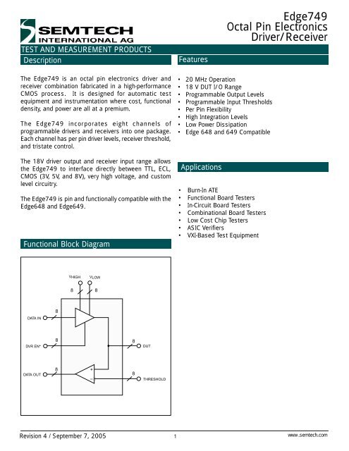
Edge749 Octal Pin Electronics Driver/Receiver - Semtech
Edge749 Octal Pin Electronics Driver/Receiver - Semtech
Edge749 Octal Pin Electronics Driver/Receiver - Semtech

You also want an ePaper? Increase the reach of your titles
YUMPU automatically turns print PDFs into web optimized ePapers that Google loves.
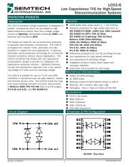
TEST AND MEASUREMENT PRODUCTS<br />
Description<br />
Features<br />
<strong>Edge749</strong><br />
<strong>Octal</strong> <strong>Pin</strong> <strong>Electronics</strong><br />
<strong>Driver</strong>/<strong>Receiver</strong><br />
The <strong>Edge749</strong> is an octal pin electronics driver and<br />
receiver combination fabricated in a high-performance<br />
CMOS process. It is designed for automatic test<br />
equipment and instrumentation where cost, functional<br />
density, and power are all at a premium.<br />
The <strong>Edge749</strong> incorporates eight channels of<br />
programmable drivers and receivers into one package.<br />
Each channel has per pin driver levels, receiver threshold,<br />
and tristate control.<br />
The 18V driver output and receiver input range allows<br />
the <strong>Edge749</strong> to interface directly between TTL, ECL,<br />
CMOS (3V, 5V, and 8V), very high voltage, and custom<br />
level circuitry.<br />
The <strong>Edge749</strong> is pin and functionally compatible with the<br />
Edge648 and Edge649.<br />
Functional Block Diagram<br />
• 20 MHz Operation<br />
• 18 V DUT I/O Range<br />
• Programmable Output Levels<br />
• Programmable Input Thresholds<br />
• Per <strong>Pin</strong> Flexibility<br />
• High Integration Levels<br />
• Low Power Dissipation<br />
• Edge 648 and 649 Compatible<br />
Applications<br />
• Burn-In ATE<br />
• Functional Board Testers<br />
• In-Circuit Board Testers<br />
• Combinational Board Testers<br />
• Low Cost Chip Testers<br />
• ASIC Verifiers<br />
• VXI-Based Test Equipment<br />
VHIGH<br />
VLOW<br />
8<br />
8<br />
8<br />
DATA IN<br />
DVR EN*<br />
8<br />
8<br />
DUT<br />
DATA OUT<br />
8<br />
+<br />
–<br />
8<br />
THRESHOLD<br />
Revision 4 / September 7, 2005<br />
1 www .semtech.com
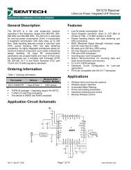
<strong>Edge749</strong><br />
TEST AND MEASUREMENT PRODUCTS<br />
PIN Description<br />
<strong>Pin</strong><br />
Name<br />
<strong>Pin</strong><br />
Number<br />
Description<br />
D ATA IN (0:7) 64, 65, 66, 67,<br />
3, 4, 5, 6<br />
D ATA OUT (0:7) 56, 57, 58, 59,<br />
11, 12, 13, 14<br />
D UT (0:7) 46, 43, 40, 37,<br />
33, 30, 27, 24<br />
D VR EN (0:7) 60, 61, 62, 63,<br />
7, 8, 9, 10<br />
V HIGH (0:7) 45, 44, 39, 38,<br />
32, 31, 26, 25<br />
V LOW (0:7) 47, 42, 41, 36,<br />
34, 29, 28, 23<br />
T HRESHOLD (0:7) 50, 51, 52, 53,<br />
17, 18, 19, 20<br />
TTL compatible inputs that determine the high/low status of the DUT<br />
drivers.<br />
CMOS level outputs that indicate the status of the DUT receivers.<br />
<strong>Pin</strong> electronic inputs/outputs that receive/drive the device under test.<br />
TTl compatible inputs that control the high impedance state of the<br />
DUT drivers.<br />
Unbuffered analog inputs that set the voltage level of a logical 1 of the<br />
DUT drivers.<br />
Unbuffered analog inputs that set the voltage level of a logical 0 of the<br />
DUT drivers.<br />
Buffered analog input voltage that sets the threshold for the DUT<br />
comparators.<br />
VCC<br />
21,<br />
49<br />
Analog positive power supply.<br />
VEE<br />
22,<br />
48<br />
Analog negative power supply.<br />
VDD<br />
1 , 15, 55<br />
Digital power supply.<br />
GND<br />
2 , 16, 54, 68<br />
Device ground.<br />
N/C<br />
35<br />
No connection.<br />
© 2005 <strong>Semtech</strong> Corp. , Rev. 4, 9/07/05 2<br />
www .semtech.com
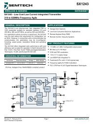
<strong>Edge749</strong><br />
TEST AND MEASUREMENT PRODUCTS<br />
PIN Description (continued)<br />
DVR EN*0<br />
DATA OUT3<br />
DATA OUT2<br />
DATA OUT1<br />
DATA OUT0<br />
VDD<br />
GND<br />
THRESHOLD3<br />
THRESHOLD2<br />
THRESHOLD1<br />
THRESHOLD0<br />
VCC<br />
VEE<br />
VLOW0<br />
DUT0<br />
VHIGH0<br />
VHIGH1<br />
DVR EN*1<br />
DUT1<br />
DVR EN*2<br />
VLOW1<br />
DVR EN*3<br />
VLOW2<br />
DATA IN0<br />
DUT2<br />
DATA IN1<br />
DATA IN2<br />
DATA IN3<br />
GND<br />
VHIGH2<br />
VHIGH3<br />
DUT3<br />
VLOW3<br />
VDD<br />
GND<br />
NC<br />
VLOW4<br />
DATA IN4<br />
DUT4<br />
DATA IN5<br />
VHIGH4<br />
DATA IN6<br />
VHIGH5<br />
DATA IN7<br />
DUT5<br />
DVR EN*4<br />
VLOW5<br />
DVR EN*5<br />
VLOW6<br />
DVR EN*6<br />
DUT6<br />
DVR EN*7<br />
DATA OUT4<br />
DATA OUT5<br />
DATA OUT6<br />
DATA OUT7<br />
VDD<br />
GND<br />
THRESHOLD4<br />
THRESHOLD5<br />
THRESHOLD6<br />
THRESHOLD7<br />
VCC<br />
VEE<br />
VLOW7<br />
DUT7<br />
VHIGH7<br />
VHIGH6<br />
10<br />
11<br />
12<br />
13<br />
14<br />
15<br />
16<br />
17<br />
18<br />
19<br />
20<br />
21<br />
22<br />
23<br />
24<br />
25<br />
26<br />
60<br />
59<br />
58<br />
57<br />
56<br />
55<br />
54<br />
53<br />
52<br />
51<br />
50<br />
49<br />
48<br />
47<br />
46<br />
45<br />
44<br />
61<br />
43<br />
62<br />
42<br />
63<br />
41<br />
64<br />
40<br />
65<br />
66<br />
67<br />
68<br />
E749<br />
68 <strong>Pin</strong> PLCC<br />
39<br />
38<br />
37<br />
36<br />
1<br />
2<br />
(Top View)<br />
35<br />
34<br />
3<br />
33<br />
4<br />
32<br />
5<br />
31<br />
6<br />
30<br />
7<br />
29<br />
8<br />
28<br />
9<br />
27<br />
© 2005 <strong>Semtech</strong> Corp. , Rev. 4, 9/07/05<br />
3 www .semtech.com
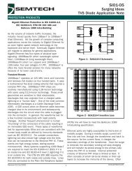
<strong>Edge749</strong><br />
TEST AND MEASUREMENT PRODUCTS<br />
Circuit Description<br />
<strong>Driver</strong> Description<br />
V HIGH and V LOW<br />
DATA IN<br />
VHIGH<br />
VLOW<br />
DUT<br />
V HIGH and V LOW define the logical “1” and “0” levels of<br />
the DUT driver and can be adjusted anywhere over the<br />
range determined by VCC and VEE. Table 1 documents<br />
the relationship between the analog power to supplies<br />
(VCC and VEE), the driver range (V HIGH and V LOW ), and<br />
the comparator threshold range (V THRESHOLD ).<br />
DVR EN*<br />
Figure 1. <strong>Driver</strong> Diagram<br />
The V HIGH and V LOW inputs are unbuffered in that they<br />
also provide the driver output current (see Figure 3), so<br />
the source of V HIGH and V LOW must have ample current<br />
drive capability.<br />
As shown in Figure 1, <strong>Edge749</strong> supports programmable<br />
high and low levels and tristate per channel. There are<br />
no shared lines between any drivers. The DVR EN* and<br />
DATA IN signals are TTL compatible inputs that control<br />
the driver (see Figure 2).<br />
VHIGH<br />
With DVR EN* high, the DUT driver goes into a high<br />
impedance state. With DVR EN* low, DATA IN high forces<br />
the driver into a high state (DUT = V HIGH ), and DATA IN<br />
low forces the driver low (DUT = V LOW ).<br />
DUT<br />
DVR EN*<br />
VLOW<br />
DATA IN<br />
DUT<br />
VHIGH<br />
VLOW<br />
Figure 3.<br />
Simplified Model of the<br />
Unbuffered Output Stage<br />
Figure 2. <strong>Driver</strong> Functionality<br />
Drive<br />
Common Mode Range<br />
Receive<br />
Common Mode Range<br />
Threshold<br />
Range<br />
VEE<br />
<strong>Edge749</strong><br />
TEST AND MEASUREMENT PRODUCTS<br />
Circuit Description (continued)<br />
<strong>Driver</strong> Output Protection<br />
In a functional testing environment, where a resistor is<br />
added in series with the driver output (to create a 50Ω<br />
output impedance), the <strong>Edge749</strong> can withstand a short<br />
to any legal DUT voltage for an indefinite amount of time.<br />
In a low impedance application with no additional output<br />
series resistance, care must be exercised and systems<br />
should be designed to check for this condition and tristate<br />
the driver if a short is detected.<br />
<strong>Receiver</strong> Functionality<br />
<strong>Edge749</strong> supports programmable thresholds per<br />
channel. There are no shared lines between comparators.<br />
THRESHOLD is a high input impedance analog input<br />
which defines a logical “1” and “0” at the DUT (see<br />
Figure 4). If the DUT voltage is more positive than<br />
THRESHOLD, DATA OUT will be high. With DUT lower<br />
than THRESHOLD, DATA OUT will be low.<br />
DATA OUT<br />
+<br />
–<br />
DUT<br />
THRESHOLD<br />
THRESHOLD<br />
DUT<br />
DATA OUT<br />
Tpd<br />
Figure 4. <strong>Receiver</strong> Functionality<br />
© 2005 <strong>Semtech</strong> Corp. , Rev. 4, 9/07/05<br />
5 www .semtech.com
<strong>Edge749</strong><br />
TEST AND MEASUREMENT PRODUCTS<br />
Application Information<br />
Power Supplies<br />
The <strong>Edge749</strong> uses three power supplies: VDD, VCC and<br />
VEE. VDD is the digital supply for all of the data inputs<br />
and outputs. VCC and VEE are the analog power supplies<br />
for the <strong>Edge749</strong> drivers and comparators. In order to<br />
protect the <strong>Edge749</strong> and avoid damaging it, the following<br />
power supply requirements must be satisifed at all times:<br />
Also,<br />
VEE ≤ GND ≤ VDD ≤ VCC<br />
VEE ≤ All Inputs ≤ VCC at all times<br />
The three-Schottky diode configuration shown in Figure<br />
5, used on a once-per-board basis, insures power supply<br />
sequence and fault tolerance.<br />
capacitor in parallel with a .001 µF chip capacitor. A<br />
VCC and VEE plane, or at least a solid power bus, is<br />
recommended for optimal performance.<br />
V HIGH and V LOW Decoupling<br />
As the V HIGH and V LOW inputs are unbuffered and must<br />
supply the driver output current, decoupling capacitors<br />
for these inputs are recommended in proportion to the<br />
amount of output current the application requires.<br />
Expanding the Common Mode Range<br />
VCC<br />
VDD<br />
1N5820 or<br />
Equivalent<br />
Although the <strong>Edge749</strong> can drive and receive 18 V swings,<br />
these 18 V signals can be adjusted over an 21 V range.<br />
By using programmable regulators V1 and V2 for the<br />
VCC and VEE supplies (feasible because these two<br />
analog power supplies do not supply driver output<br />
current), the <strong>Edge749</strong> I/O range can be optimized for a<br />
variety of applications (see Figure 6).<br />
V1<br />
VEE<br />
Figure 5. Power Supply Protection Scheme<br />
Power-On Sequencing Power-Off Sequencing<br />
1. VCC (substrate) 1. Inputs<br />
2. VEE 2. VDD<br />
3. VDD 3. VEE<br />
4. Inputs 4. VCC<br />
Power Supplies Decoupling<br />
V2<br />
VCC<br />
Edge 749<br />
VDD<br />
Figure 6.<br />
VDD, which provides the digital power, should be<br />
decoupled to GND with a .1 µF chip capacitor in parallel<br />
with a .001 µF chip capacitor. The bypass capacitors<br />
should be as close to the device as possible. Power and<br />
ground planes are recommended to provide a low<br />
inductance return path.<br />
There are three rules which govern the supplies V1 and<br />
V2:<br />
1) +10V < V1 < +18V<br />
2) –3V < V2 < 0V<br />
3) (V1 – V2) < +18V.<br />
VCC and VEE, which power the DUT drivers and receivers,<br />
should also be decoupled to GND with a .1 µF chip<br />
© 2005 <strong>Semtech</strong> Corp. , Rev. 4, 9/07/05 6<br />
www .semtech.com
<strong>Edge749</strong><br />
TEST AND MEASUREMENT PRODUCTS<br />
Application Information (continued)<br />
Window Comparator<br />
Certain applications require a dual threshold window<br />
comparator to distinguish between the DUT being high,<br />
low, or floating. To support this application, two <strong>Edge749</strong><br />
channels can be combined to create one channel with a<br />
window comparator (see Figure 7). Notice that<br />
connecting two DUT pins ties together the positive inputs<br />
of both receivers. The result is a difference in polarity<br />
between the digital outputs reporting the high and low<br />
status of the DUT.<br />
DUT HIGH<br />
DUT LOW*<br />
–<br />
+<br />
+<br />
–<br />
Figure 7. <strong>Edge749</strong> as a<br />
Window Comparator<br />
High Threshold<br />
DUT<br />
Low Threshold<br />
Once two receivers are connected as window<br />
comparators, the two drivers also get connected in<br />
parallel. This dual driver configuration supports a<br />
multitude of applications that have traditionally been<br />
difficult to accommodate.<br />
Trinary <strong>Driver</strong><br />
At times, there is a need for a three-level driver. Typically,<br />
two levels are required for the standard digital “1” and<br />
“0” pattern generation. The third level provides a higher<br />
voltage to place the device under test (DUT) into a<br />
programming or test mode. By controlling the DATA IN<br />
and DVR EN* inputs, a trinary driver with tristate is<br />
realizable (see Figure 8).<br />
<strong>Driver</strong> with Pull Up/Pull Down<br />
As the drivers are unbuffered, paralleling two drivers for<br />
one DUT node provides a means for adding pull up or<br />
pull down capability. By connecting the V HIGH and V LOW<br />
inputs of one driver through a resistor to a voltage,<br />
additional functionality that would normally require an<br />
external relay on the DUT transmission line to engage<br />
and disengage these functions is realizable.<br />
One common application for the pull up feature is testing<br />
open collector devices. The pull down satisfies open<br />
emitter DUTs (typically ECL). Either the pull up or down<br />
could be used to establish a default high impedance<br />
voltage on a bidirectional bus. Notice that in all<br />
applications, the resistors can be switched dynamically<br />
or statically.<br />
VHIGH A<br />
VLOW A<br />
DATA IN A<br />
DVR EN*A<br />
VHIGH B<br />
DUT<br />
VHIGH B<br />
VHIGH A<br />
VLOW A<br />
DATA IN B<br />
DVR EN*B<br />
Figure 8. Trinary <strong>Driver</strong><br />
© 2005 <strong>Semtech</strong> Corp. , Rev. 4, 9/07/05<br />
7 www .semtech.com
<strong>Edge749</strong><br />
TEST AND MEASUREMENT PRODUCTS<br />
Application Information (continued)<br />
Also, either the pull up or pull down resistor could be<br />
used to terminate the transmission from the DUT to the<br />
pin electronics in an effort to minimize any reflections.<br />
DATA IN A<br />
DVR EN*A<br />
DATA IN B<br />
DVR EN*B<br />
Figure 9. <strong>Driver</strong> with Pull Up/Pull Down<br />
Trinary <strong>Driver</strong> with Termination<br />
Other combinations are also possible. For example, two<br />
parallel drivers can be configured to implement one<br />
trinary driver with a pull down (or pull up) dynamic<br />
termination (see Figure 10).<br />
DATA IN A<br />
VHIGH A<br />
VHIGH A<br />
VHIGH B<br />
VLOW B<br />
VLOW A<br />
VLOW A<br />
VPULL UP<br />
VPULL DOWN<br />
DUT<br />
Two Logic Family <strong>Driver</strong><br />
Many test systems support exactly two families of driver<br />
and receiver levels and select between family A and family<br />
B settings on a per-pin basis, typically using an analog<br />
multiplexer (See Figure 11). Common examples of these<br />
families are:<br />
Family A = TTL<br />
Family B = CMOS<br />
or<br />
Family A = TTL<br />
Family B = ECL<br />
The <strong>Edge749</strong> supports this system architecture with<br />
minimal hardware and the elimination of the per-pin<br />
analog multiplexer. The drive and receive levels need to<br />
be generated once per system, then distributed and<br />
buffered suitably.<br />
Parametric Functions<br />
Two drivers in parallel also offer the possibility of<br />
connecting force and sense parametric circuitry to the<br />
DUT without adding additional circuitry to the controlled<br />
impedance DUT line. For example, Figure 12 shows the<br />
second driver being utilized to force a current and<br />
measure a voltage.<br />
DVR EN*A<br />
DATA IN B<br />
VHIGH B<br />
VTERMINATION<br />
DUT<br />
Notice that the V HIGH and V LOW pins are used from<br />
different drivers to allow the force and sense functions<br />
to be active simultaneously.<br />
DVR EN*B<br />
Figure 10. Trinary <strong>Driver</strong> with Termination<br />
© 2005 <strong>Semtech</strong> Corp. , Rev. 4, 9/07/05 8<br />
www .semtech.com
<strong>Edge749</strong><br />
TEST AND MEASUREMENT PRODUCTS<br />
Application Information (continued)<br />
CHANNEL 1<br />
CHANNEL n<br />
VHIGH A<br />
VHIGH B<br />
DVR EN*A<br />
DVR EN*A<br />
DVR DATA<br />
DVR DATA<br />
DVR EN*B<br />
DUT0<br />
DVR EN*B<br />
DUT0<br />
VLOW B<br />
VLOW A<br />
Figure 11. Family A/B Using Two <strong>Driver</strong>s Per <strong>Pin</strong><br />
<strong>Driver</strong> Output Impedance<br />
<strong>Edge749</strong> Ron vs. Vout - VCC=+16.5V, VEE=-1.5V<br />
Ideally, a driver would have a constant<br />
output impedance over all ouptut<br />
conditions. However, the <strong>Edge749</strong><br />
ouptut impedance does vary slightly<br />
over the common mode drive level and<br />
whether it is driving high or low. Figure<br />
12 shows the variation in Rout.<br />
Ron [Ohms]<br />
9.5<br />
9<br />
8.5<br />
8<br />
7.5<br />
7<br />
6.5<br />
6<br />
R_VLO<br />
R_VHI<br />
-1.5<br />
-0.5<br />
0.5<br />
1.5<br />
2.5<br />
3.5<br />
4.5<br />
5.5<br />
6.5<br />
7.5<br />
8.5<br />
9.5<br />
10.5<br />
11.1<br />
12.5<br />
13.5<br />
14.5<br />
15.5<br />
16.5<br />
Vout [V]<br />
Figure 12. ROUT vs. DOUT<br />
<strong>Edge749</strong> Leakage in HIZ - VCC=+16.5V, VEE=-1.5V<br />
10<br />
High Impedance Leakage<br />
8<br />
6<br />
The <strong>Edge749</strong> is designed to be<br />
extremely low leakage (see Figure 13.)<br />
In a low performance application, where<br />
the output capacitance is not a concern,<br />
the low leakage may allow the<br />
elimination of an isolation relay.<br />
Leakage Current [nA]<br />
4<br />
2<br />
0<br />
-2<br />
-4<br />
-6<br />
-8<br />
VLO=0, VHI=+8<br />
-10<br />
-3<br />
-2<br />
-1<br />
0<br />
1<br />
2<br />
3<br />
4<br />
5<br />
6<br />
7<br />
8<br />
9<br />
10<br />
11<br />
12<br />
13<br />
14<br />
15<br />
16<br />
17<br />
Dout [Volts]<br />
Figure 13. High Impedance Leakage<br />
© 2005 <strong>Semtech</strong> Corp. , Rev. 4, 9/07/05<br />
9 www .semtech.com
<strong>Edge749</strong><br />
TEST AND MEASUREMENT PRODUCTS<br />
Package Information<br />
68 <strong>Pin</strong> PLCC Package<br />
θJA = 42 to 48˚C / W<br />
PIN Descriptions<br />
0.990 SQ<br />
[25.146]<br />
0.048<br />
[1.219]<br />
See Detail A<br />
0.953 SQ<br />
[24.206]<br />
0.045 SQ<br />
[1.143]<br />
0.800 REF<br />
[20.32]<br />
0.910<br />
[23.114]<br />
0.175<br />
[4.445]<br />
0.113<br />
[2.87]<br />
0.029<br />
[0.736]<br />
0.016<br />
[0.406]<br />
0.016<br />
[0.406]<br />
0.020<br />
[0.508]<br />
MIN<br />
;<br />
;<br />
;<br />
0.029<br />
[0.736]<br />
0.030<br />
[0.762]<br />
0.065<br />
[1.651]<br />
Notes: (unless otherwise specified)<br />
1. Dimensions are in inches [millimeters].<br />
2. Tolerances are: .XXX ± 0.005 [0.127].<br />
3. PLCC packages are intended for surface mounting on solder lands on 0.050 [1.27] centers.<br />
© 2005 <strong>Semtech</strong> Corp. , Rev. 4, 9/07/05 10<br />
www .semtech.com
<strong>Edge749</strong><br />
TEST AND MEASUREMENT PRODUCTS<br />
Recommended Operating Conditions<br />
Parameter<br />
Symbol<br />
Min<br />
Typ<br />
Max<br />
Units<br />
Digital<br />
Analog<br />
Analog<br />
Total<br />
Power Supply<br />
Positive Power Supply<br />
Negative Power Supply<br />
Analog Power Supply<br />
VDD<br />
4.<br />
5<br />
5 5.<br />
5 V<br />
VCC<br />
10<br />
15<br />
18<br />
V<br />
VEE<br />
-3<br />
-2<br />
0 V<br />
VCC - VEE<br />
10<br />
18<br />
V<br />
D river High Output Voltage<br />
V HIG<br />
H<br />
D river Low Output Voltage<br />
V LO<br />
W<br />
T otal <strong>Driver</strong> Output Swing<br />
V HIG<br />
H - VLOW<br />
-18<br />
18<br />
V<br />
<strong>Receiver</strong><br />
Threshold Voltage<br />
VEE<br />
VEE<br />
VCC<br />
VCC<br />
THRESHOLD<br />
VEE<br />
+ 3<br />
VCC - 3<br />
V<br />
V<br />
V<br />
Ambient<br />
Operating Temperature<br />
TA<br />
TJ<br />
0<br />
0<br />
+70<br />
+125<br />
o C<br />
o C<br />
Absolute Maximum Ratings<br />
Parameter<br />
Symbol<br />
Min<br />
Typ<br />
Max<br />
Units<br />
Total<br />
Positive<br />
Negative<br />
Analog Power Supply<br />
Analog Power Supply<br />
Analog Power Supply<br />
VCC - VEE<br />
19<br />
V<br />
VCC<br />
-.<br />
5<br />
19<br />
V<br />
VEE<br />
-5<br />
0.<br />
5 V<br />
<strong>Driver</strong><br />
High Output Voltage<br />
VHIGH<br />
VEE<br />
- . 5<br />
VCC + . 5<br />
<strong>Driver</strong><br />
Low Output Voltage<br />
V LOW<br />
VEE<br />
- . 5<br />
VCC + . 5<br />
D river Output Swing<br />
V HIG<br />
H - VLOW<br />
-18.<br />
5<br />
18.<br />
5 V<br />
<strong>Receiver</strong><br />
Threshold Voltage<br />
THRESHOLD<br />
VEE<br />
- . 5<br />
VCC + . 5<br />
V<br />
V<br />
V<br />
Digital<br />
Inputs<br />
DATA IN<br />
DVR EN*<br />
GND - .5<br />
VDD + . 5<br />
V<br />
Digital<br />
Ambient<br />
Storage<br />
Junction<br />
Soldering<br />
Power Supply<br />
Operating Temperature<br />
Temperature<br />
Temperature<br />
Temperature<br />
VDD<br />
0 6.<br />
5 V<br />
TA<br />
-55<br />
+ 125<br />
o C<br />
TS<br />
-65<br />
+ 150<br />
o C<br />
TJ<br />
+ 150<br />
o C<br />
TSOL<br />
260<br />
o C<br />
Stresses above those listed under "Absolute Maximum Ratings" may cause permanent damage to the<br />
device. This is a stress rating only, and functional operation of the device at these, or any other conditions<br />
beyond those listed, is not implied. Exposure to absolute maximum conditions for extended periods may<br />
affect device reliability.<br />
© 2005 <strong>Semtech</strong> Corp. , Rev. 4, 9/07/05<br />
11 www .semtech.com
<strong>Edge749</strong><br />
TEST AND MEASUREMENT PRODUCTS<br />
DC Characteristics<br />
Parameter<br />
Symbol<br />
Min<br />
Typ<br />
Max<br />
Units<br />
<strong>Driver</strong>/<strong>Receiver</strong> Characteristics<br />
O utput Voltage Swing<br />
V HIG<br />
H - VLOW<br />
-18<br />
18<br />
V<br />
DC <strong>Driver</strong> Output Current (Note 1) IOUT<br />
-125<br />
+ 125<br />
mA<br />
Output<br />
Impedance (Note 2)<br />
R OUT<br />
4 8 12<br />
Ω<br />
DUT<br />
<strong>Pin</strong> Capacitance<br />
C OUT<br />
20<br />
pF<br />
D UT Output voltage<br />
DUT<br />
<strong>Receiver</strong><br />
Threshold Level<br />
VTHRESHOLD<br />
VEE<br />
+ 3<br />
VCC - 3<br />
Threshold<br />
Bias Current<br />
0 1.<br />
0 µ A<br />
DUT<br />
Leakage Input Current<br />
IBIAS<br />
. 001<br />
1.<br />
0 µ A<br />
<strong>Receiver</strong><br />
Offset Voltage (Note 3)<br />
VEE<br />
VCC<br />
VOS<br />
-200<br />
200<br />
mV<br />
V<br />
V<br />
Quiescent Power Supply Current<br />
Positive Power Supply<br />
Negative Power Supply<br />
Digital Power Supply<br />
ICC<br />
IEE<br />
IDD<br />
-60<br />
60<br />
-40<br />
5<br />
80<br />
15<br />
mA<br />
mA<br />
mA<br />
Digital Inputs<br />
DATA IN (0:7), DVR EN* (0:7)<br />
Input<br />
Input<br />
Input<br />
Input<br />
High Voltage<br />
Low Voltage<br />
Current<br />
Capacitance<br />
Digital Outputs<br />
DATA OUT (0:7)<br />
VIHMIN<br />
2.<br />
0<br />
VDD<br />
VILMAX<br />
0 0.<br />
8 V<br />
I IN<br />
1.<br />
0 µ A<br />
C IN<br />
5 pF<br />
V<br />
Output<br />
Voltage High (Note 4)<br />
VOH<br />
VDD - . 4<br />
VDD + . 4<br />
V<br />
Output<br />
Voltage Low (Note 5)<br />
VOL<br />
-0.<br />
4<br />
0 0.<br />
4 V<br />
DC Output current<br />
IOUT<br />
4 mA<br />
Note 1 : Output current specification is per individual driver.<br />
Note 2 : Tested for driving a high state and low state at +18V, +6V, and 0V.<br />
Note 3 : Measured at THRESHOLD = +1.5V.<br />
Note 4: Output current of –4 mA.<br />
Note 5: Output current of 4 mA.<br />
© 2005 <strong>Semtech</strong> Corp. , Rev. 4, 9/07/05 12<br />
www .semtech.com
<strong>Edge749</strong><br />
TEST AND MEASUREMENT PRODUCTS<br />
AC Characteristics<br />
Parameter<br />
Symbol<br />
Min<br />
Typ<br />
Max<br />
Units<br />
Propagation Delay<br />
DATA IN to DUT <br />
DUT to DATA OUT <br />
Active to HiZ<br />
HiZ to Active<br />
T1<br />
T2<br />
T3<br />
T4<br />
20<br />
10<br />
20<br />
20<br />
29<br />
21<br />
32<br />
28<br />
38<br />
30<br />
40<br />
35<br />
ns<br />
ns<br />
ns<br />
ns<br />
DUT Output Rise/Fall Times (Note 1)<br />
1V Swing (20% - 80%)<br />
3V Swing (10% - 90%)<br />
5V Swing (10% - 90%)<br />
8V Swing (10% - 90%)<br />
10V Swing (10% - 90%)<br />
1.0<br />
1.5<br />
1.5<br />
1.5<br />
1.5<br />
ns<br />
ns<br />
ns<br />
ns<br />
ns<br />
Digital Outputs (DATA OUT )<br />
DATA OUT Rise Time (10% - 90%)<br />
DATA OUT Fall Time (10% - 90%)<br />
TR<br />
TF<br />
2.5<br />
2.5<br />
ns<br />
ns<br />
Minimum Pulse Width<br />
<strong>Driver</strong> Output<br />
Comparator Output<br />
25<br />
20<br />
20<br />
15<br />
ns<br />
ns<br />
Maximum Operating<br />
Frequency<br />
Fmax<br />
15<br />
20<br />
MHz<br />
Note 1:<br />
Into 18 inches of 50Ω transmission line terminated with 1KΩ and 5 pF with the proper<br />
series termination resistor.<br />
T1<br />
T2<br />
DATA IN<br />
DUT<br />
DATA OUT<br />
DVR EN*<br />
DUT<br />
HiZ<br />
T3<br />
T4<br />
© 2005 <strong>Semtech</strong> Corp. , Rev. 4, 9/07/05<br />
13 www .semtech.com
<strong>Edge749</strong><br />
TEST AND MEASUREMENT PRODUCTS<br />
Ordering Information<br />
Model<br />
Number<br />
Package<br />
E749BPJ<br />
68-<strong>Pin</strong> PLCC<br />
EVM749EVM<br />
<strong>Edge749</strong> Evaluation Module<br />
Contact Information for <strong>Semtech</strong> International AG<br />
Taiwan Branch<br />
Tel: 886-2-2748-3380<br />
Fax: 886-2-2748-3390<br />
<strong>Semtech</strong> Switzerland GmbH<br />
Japan Branch<br />
Tel: 81-3-6408-0950<br />
Fax: 81-3-6408-0951<br />
Korea Branch<br />
Tel: 82-2-527-4377<br />
Fax: 82-2-527-4376<br />
<strong>Semtech</strong> Limited (U.K.)<br />
Tel: 44-1794-527-600<br />
Fax: 44-1794-527-601<br />
Shanghai Office<br />
Tel: 86-21-6391-0830<br />
Fax: 86-21-6391-0831<br />
<strong>Semtech</strong> France SARL<br />
Tel: 33-(0)169-28-22-00<br />
Fax: 33-(0)169-28-12-98<br />
<strong>Semtech</strong> International AG is a wholly-owned subsidiary of<br />
<strong>Semtech</strong> Corporation, which has its headquarters in the U.S.A.<br />
<strong>Semtech</strong> Germany GmbH<br />
Tel: 49-(0)8161-140-123<br />
Fax: 49-(0)8161-140-124<br />
© 2005 <strong>Semtech</strong> Corp. , Rev. 4, 9/07/05 14<br />
www .semtech.com