Edge4717D Quad Channel, Per Pin Precision ... - Semtech
Edge4717D Quad Channel, Per Pin Precision ... - Semtech
Edge4717D Quad Channel, Per Pin Precision ... - Semtech

You also want an ePaper? Increase the reach of your titles
YUMPU automatically turns print PDFs into web optimized ePapers that Google loves.
TEST AND MEASUREMENT PRODUCTS<br />
Description<br />
The <strong>Edge4717D</strong> is a precision measurement unit designed<br />
for automated test equipment and instrumentation.<br />
Manufactured in a wide voltage CMOS process, it is a<br />
monolithic solution for a quad channel per pin PMU.<br />
Each channel of the <strong>Edge4717D</strong> features a PMU that<br />
can force or measure voltage over a typical 15V I/O range,<br />
and supports 4 current ranges: ± 3.2 µA, ± 80 µA,<br />
± 2 mA, ± 30 mA.<br />
The <strong>Edge4717D</strong> has an on-board window comparator per<br />
channel that provides two bits of information — DUT too<br />
high and DUT too low. There is also a monitor pin which<br />
provides a real time analog signal proportional to either<br />
the voltage or current measured at the DUT.<br />
The <strong>Edge4717D</strong> is designed to be a low power, low cost,<br />
small footprint solution to allow high pin count testers to<br />
support a PMU per pin.<br />
On-board voltage clamps, with over-current detection,<br />
provide protection to the DUT and 4717D.<br />
The <strong>Edge4717D</strong> also has a sample-and-hold feature<br />
available for capturing DUT current or voltage<br />
measurements.<br />
The <strong>Edge4717D</strong> is a design improvement to the Edge4717<br />
that features:<br />
– Increased FV/MV range<br />
– Improved over-current detection circuit<br />
functionality<br />
– LVTTL comparator outputs (pull-up resistors<br />
no longer required)<br />
– Improved HiZ switching characteristics<br />
– Improved Force Voltage Linearity<br />
Applications<br />
• Automated Test Equipment<br />
- Memory Testers<br />
- VLSI Testers<br />
- Mixed Signal Tester<br />
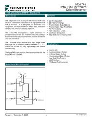
<strong>Edge4717D</strong><br />
<strong>Quad</strong> <strong>Channel</strong>, <strong>Per</strong> <strong>Pin</strong><br />
<strong>Precision</strong> Measurement Unit<br />
Features<br />
• FV / MI Capability<br />
• FI / MV Capability<br />
• FV / MV Capability<br />
• FI / MI Capability<br />
• 4 Current Ranges (± 3.2 µA, ± 80 µA, ± 2 mA,<br />
± 30 mA)<br />
• –5.5V to 9.5V Nominal Output Range (Zero Current)<br />
• –3.5 to 7.5V Nominal Output Range (Full Scale<br />
Current)<br />
• On-board Voltage Clamps<br />
• Internal Sample and Hold<br />
• 228 <strong>Pin</strong> 23 mm x 23 mm TBGA Package<br />
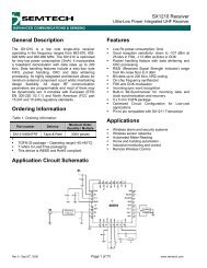
Functional Block Diagram<br />
SNK_MON<br />
SRC_MON<br />
HiZ<br />
VINP<br />
FV / FI*<br />
MI / MV*<br />
IVMAX<br />
IVMIN<br />
COMP_IN<br />
DISABLE<br />
SNK_MON<br />
SRC_MON<br />
HiZ<br />
VINP<br />
FV / FI*<br />
MI / MV*<br />
IVMAX<br />
IVMIN<br />
COMP_IN<br />
DISABLE<br />
SNK_MON<br />
SRC_MON<br />
HiZ<br />
VINP<br />
FV / FI*<br />
MI / MV*<br />
IVMAX<br />
IVMIN<br />
COMP_IN<br />
DISABLE<br />
SNK_MON<br />
SRC_MON<br />
HiZ<br />
VINP<br />
FV / FI*<br />
MI / MV*<br />
IVMAX<br />
IVMIN<br />
COMP_IN<br />
DISABLE<br />
CHANNEL 0<br />
COMPARATORS<br />
DETECTOR LOGIC<br />
VOLTAGE MONITOR<br />
OVER-CURRENT<br />
DETECT<br />
OVER-CURRENT<br />
DETECT<br />
DUT_GND<br />
SNK_OUT<br />
OPEN_RLY<br />
SRC_OUT<br />
FORCE<br />
REF ÷ 2.5 GUARD<br />
CHANNEL 1<br />
COMPARATORS<br />
DETECTOR LOGIC<br />
VOLTAGE MONITOR<br />
OVER-CURRENT<br />
DETECT<br />
OVER-CURRENT<br />
DETECT<br />
SENSE<br />
DUTLTH<br />
DUTGTL<br />
IVMON<br />
SNK_OUT<br />
OPEN_RLY<br />
SRC_OUT<br />
FORCE<br />
REF ÷ 2.5 GUARD<br />
CHANNEL 2<br />
COMPARATORS<br />
DETECTOR LOGIC<br />
VOLTAGE MONITOR<br />
OVER-CURRENT<br />
DETECT<br />
OVER-CURRENT<br />
DETECT<br />
SENSE<br />
DUTLTH<br />
DUTGTL<br />
IVMON<br />
SNK_OUT<br />
OPEN_RLY<br />
SRC_OUT<br />
FORCE<br />
REF ÷ 2.5 GUARD<br />
CHANNEL 3<br />
COMPARATORS<br />
DETECTOR LOGIC<br />
VOLTAGE MONITOR<br />
OVER-CURRENT<br />
DETECT<br />
OVER-CURRENT<br />
DETECT<br />
SENSE<br />
DUTLTH<br />
DUTGTL<br />
IVMON<br />
SNK_OUT<br />
OPEN_RLY<br />
SRC_OUT<br />
FORCE<br />
REF ÷ 2.5 GUARD<br />
SENSE<br />
DUTLTH<br />
DUTGTL<br />
IVMON<br />
Revision 5 / October 14, 2005<br />
1 www.semtech.com
<strong>Edge4717D</strong><br />
TEST AND MEASUREMENT PRODUCTS<br />
PIN Description<br />
P in Name<br />
<strong>Pin</strong><br />
#<br />
VINP[0:3]<br />
B19,<br />
H22, N21, V22<br />
REF[0:3]<br />
A19,<br />
G22, M21, U22<br />
Description<br />
Analog voltage input which forces the output<br />
output current (FI mode) (one per channel).<br />
Reference pin for divide by<br />
is typically set to 2.25V.<br />
voltage (FV mode) and the<br />
2.5 circuit for force current mode; this reference<br />
FORCE[0:3]<br />
E 2, J2, N2, U2<br />
Analog output pin which forces current or voltage.<br />
SENSE[0:3]<br />
E 3, J3, N3, U3<br />
Analog input pin which senses voltage.<br />
FV_FI*[0:3]<br />
A7,<br />
C11, A14, B17<br />
MI_MV*[0:3]<br />
C9,<br />
B11, B14, C16<br />
TTL compatible input<br />
or forcing voltage.<br />
TTL compatible input which determines<br />
current or measuring voltage.<br />
which determines whether the PMU is forcing current<br />
whether the PMU is measuring<br />
RS0[0:3]<br />
C 7, B9, C12, B15<br />
TTL compatible current range select inputs.<br />
RS1[0:3]<br />
C 6, A8, B12, A15<br />
TTL compatible current range select inputs.<br />
IVMIN[0:3]<br />
C17,<br />
H20, M20, U21<br />
IVMAX[0:3]<br />
C18,<br />
H21, N22, U20<br />
Analog input voltages which<br />
measurement comparator.<br />
Analog input voltages which<br />
measurement comparator.<br />
establish the lower threshold level for the<br />
establish the upper threshold level for the<br />
COMP_IN[0:3]<br />
D 2, H2, M2, T2<br />
Analog voltage input to measurement comparator.<br />
DUT_LTH[0:3]<br />
AA13,<br />
Y12, AA10, Y9<br />
DUT_GTL[0:3]<br />
AA14,<br />
AA12, Y11, AA9<br />
DISABLE[0:3]<br />
A6, B10, B13, B16<br />
HIZ[0:3]<br />
B7, A10, C13, A17<br />
Digital comparator output<br />
the upper threshold.<br />
Digital comparator output<br />
than the lower threshold.<br />
that indicates the DUT measurement is less than<br />
that indicates the DUT measurement is greater<br />
TTL compatible input which places IVMON output in high impedance.<br />
TTL compatible input that places the FORCE output into high impedance.<br />
RA[0:3]<br />
F 3, K3, P3, V3<br />
External resistor input corresponding to Range A.<br />
RB[0:3]<br />
F 2, K2, P2, V2<br />
External resistor input corresponding to Range B.<br />
RC[0:3]<br />
F 1, K1, P1, V1<br />
External resistor input corresponding to Range C.<br />
RD[0:3]<br />
G 3, L3, R3, W3<br />
External resistor input corresponding to Range D.<br />
SNK_MON[0:3]<br />
F 21, K22, R22, AA17<br />
Analog voltage input to sink current clamp.<br />
SRC_MON[0:3]<br />
F 22, L22, T22, Y16<br />
Analog voltage input to source current clamp.<br />
SNK_OUT[0:3]<br />
C 1, G1, L1, R1<br />
Clamp output.<br />
SRC_OUT[0:3]<br />
E 1, J1, N1, U1<br />
Clamp output.<br />
© 2005 <strong>Semtech</strong> Corp. / Rev. 5, 10/14/05<br />
2<br />
www.semtech.com
<strong>Edge4717D</strong><br />
TEST AND MEASUREMENT PRODUCTS<br />
PIN Description (continued)<br />
P in Name<br />
<strong>Pin</strong><br />
#<br />
OPEN_RLY[0:3]<br />
Y14,<br />
Y13, AA11, Y10<br />
IVMON[0:3]<br />
B18,<br />
G21, M22, T21<br />
Description<br />
Open drain output that is used for opening<br />
in case of an over-current condition.<br />
Analog voltage output that provides a real time<br />
measured voltage or measured current level.<br />
relays between tester and DUT<br />
monitor of either the<br />
LTCH_MODE[0:3]<br />
B6,<br />
C10, A12, A16<br />
Controls a mux for determination of whether IVMONITOR is from sample-<br />
and-hold or not sampled.<br />
SAMPLE[0:3]<br />
C8, A9, A13, C15<br />
Used for sampling the voltage on the SENSE[0:3] voltage monitor pins.<br />
GUARD[0:3]<br />
D 1, H1, M1, T1<br />
Driven guard pin used for guard traces.<br />
TEST[0:3]<br />
B 8, A11, C14, A18<br />
Digital input control pin for mux for testing sample-and-hold.<br />
TEST_IN[0:3]<br />
C 19, J22, N20, V21<br />
Analog input for testing the sample-and-hold.<br />
COMP1[0:3]<br />
COMP2[0:3]<br />
D20, J20, P21, V20<br />
D21, J21, P20, Y19<br />
Internal compensation pins that require an external capacitor connection<br />
between the two pins.<br />
COMP3[0:3]<br />
E21,<br />
K21, R21, Y18<br />
COMP4[0:3]<br />
F20,<br />
K20, R20, Y17<br />
Internal compensation pin that<br />
between the pin and ground.<br />
Internal compensation pin that requires<br />
between the pin and FORCE output.<br />
requires an external capacitor connection<br />
an external capacitor connection<br />
DUT_GND<br />
Y 6<br />
Input reference pin that should be connected to DUT ground line.<br />
Power <strong>Pin</strong>s<br />
V CC<br />
A1, A2, A21, A22,<br />
B1, B2, B21, B22,<br />
C3, C20, Y3, Y20, AA1,<br />
AA2, AA21, AA22, AB1,<br />
AB2, AB21, AB22<br />
Positive analog power supply.<br />
VDD<br />
Y 15<br />
Positive digital supply (comparator).<br />
V EE<br />
A20, B20, C21, C22,<br />
D22, E22, G2, L2, R2,<br />
W2, W21, W22, Y21, Y22,<br />
AA15, AA18, AA19, AA20,<br />
AB13, AB14, AB15, AB16,<br />
AB17, AB18, AB19, AB20<br />
G ND<br />
A3, A4, A5, B3, B4, B5,<br />
C2, C4, C5, W1, Y1, Y2,<br />
Y4, Y5, Y7, Y8, AA3, AA4,<br />
AA5, AA6, AA7, AA8, AB3,<br />
AB4, AB5, AB6, AB7, AB8,<br />
AB9, AB10, AB11, AB12<br />
Negative analog power supply.<br />
Ground.<br />
N C<br />
D3, E20, H3, G20, L20,<br />
L21, M3, P22, T3, T20,<br />
W20, AA16<br />
No Connection.<br />
(Unused pins; leave unconnected).<br />
© 2005 <strong>Semtech</strong> Corp. / Rev. 5, 10/14/05<br />
3<br />
www.semtech.com
4<br />
© 2005 <strong>Semtech</strong> Corp. / Rev. 5, 10/14/05<br />
TEST AND MEASUREMENT PRODUCTS<br />
<strong>Edge4717D</strong><br />
www.semtech.com<br />
PIN Description (continued)<br />
Top View<br />
23mm x 23mm 228 <strong>Pin</strong> TBGA<br />
A1 Ball Pad<br />
Indicator<br />
E4717<br />
228 <strong>Pin</strong> TBGA<br />
23mm x 23mm<br />
SEMTECH<br />
1 2 3 4 5 6 7 8 9 10 11 12 13 14 15 16 17 18 19 20 21 22<br />
A<br />
B<br />
C<br />
D<br />
E<br />
F<br />
G<br />
H<br />
J<br />
K<br />
L<br />
M<br />
N<br />
P<br />
R<br />
T<br />
U<br />
V<br />
W<br />
Y<br />
AA<br />
AB<br />
A1<br />
B1<br />
C1<br />
Y1<br />
AA1<br />
AB1<br />
D1<br />
E1<br />
F1<br />
G1<br />
H1<br />
J1<br />
K1<br />
L1<br />
M1<br />
N1<br />
P1<br />
R1<br />
T1<br />
U1<br />
V1<br />
W1<br />
VCC<br />
GUARD0<br />
SRC_OUT0<br />
RC0<br />
SNK_OUT1<br />
GUARD1<br />
SRC_OUT1<br />
RC1<br />
SNK_OUT2<br />
GUARD2<br />
SRC_OUT2<br />
RC2<br />
SNK_OUT3<br />
GUARD3<br />
SRC_OUT3<br />
RC3<br />
GND<br />
VCC<br />
SNK_OUT0<br />
GND<br />
VCC<br />
VCC<br />
A2<br />
B2<br />
C2<br />
Y2<br />
AA2<br />
AB2<br />
D2<br />
E2<br />
F2<br />
G2<br />
H2<br />
J2<br />
K2<br />
L2<br />
M2<br />
N2<br />
P2<br />
R2<br />
T2<br />
U2<br />
V2<br />
W2<br />
VCC<br />
COMP_IN0<br />
FORCE0<br />
RB0<br />
VEE<br />
COMP_IN1<br />
FORCE1<br />
RB1<br />
VEE<br />
COMP_IN2<br />
FORCE2<br />
RB2<br />
VEE<br />
COMP_IN3<br />
FORCE3<br />
RB3<br />
VEE<br />
VCC<br />
GND<br />
GND<br />
VCC<br />
VCC<br />
A3<br />
B3<br />
C3<br />
Y3<br />
AA3<br />
AB3<br />
D3<br />
E3<br />
F3<br />
G3<br />
H3<br />
J3<br />
K3<br />
L3<br />
M3<br />
N3<br />
P3<br />
R3<br />
T3<br />
U3<br />
V3<br />
W3<br />
GND<br />
NC<br />
SENSE0<br />
RA0<br />
RD0<br />
NC<br />
SENSE1<br />
RA1<br />
RD1<br />
NC<br />
SENSE2<br />
RA2<br />
RD2<br />
NC<br />
SENSE3<br />
RA3<br />
RD3<br />
GND<br />
VCC<br />
VCC<br />
GND<br />
GND<br />
A4<br />
B4<br />
C4<br />
Y4<br />
AA4<br />
AB4<br />
D4<br />
E4<br />
F4<br />
G4<br />
H4<br />
J4<br />
K4<br />
L4<br />
M4<br />
N4<br />
P4<br />
R4<br />
T4<br />
U4<br />
V4<br />
W4<br />
GND<br />
GND<br />
GND<br />
GND<br />
GND<br />
GND<br />
A5<br />
B5<br />
C5<br />
Y5<br />
AA5<br />
AB5<br />
D5<br />
E5<br />
F5<br />
G5<br />
H5<br />
J5<br />
K5<br />
L5<br />
M5<br />
N5<br />
P5<br />
R5<br />
T5<br />
U5<br />
V5<br />
W5<br />
GND<br />
GND<br />
GND<br />
GND<br />
GND<br />
GND<br />
A6<br />
B6<br />
C6<br />
Y6<br />
AA6<br />
AB6<br />
D6<br />
E6<br />
F6<br />
G6<br />
H6<br />
J6<br />
K6<br />
L6<br />
M6<br />
N6<br />
P6<br />
R6<br />
T6<br />
U6<br />
V6<br />
W6<br />
DISABLE0<br />
LTCH_MODE0<br />
RS10<br />
DUT_GND<br />
GND<br />
GND<br />
A7<br />
B7<br />
C7<br />
Y7<br />
AA7<br />
AB7<br />
D7<br />
E7<br />
F7<br />
G7<br />
H7<br />
J7<br />
K7<br />
L7<br />
M7<br />
N7<br />
P7<br />
R7<br />
T7<br />
U7<br />
V7<br />
W7<br />
FV_FIN0<br />
HIZ0<br />
RS00<br />
GND<br />
GND<br />
GND<br />
A8<br />
B8<br />
C8<br />
Y8<br />
AA8<br />
AB8<br />
D8<br />
E8<br />
F8<br />
G8<br />
H8<br />
J8<br />
K8<br />
L8<br />
M8<br />
N8<br />
P8<br />
R8<br />
T8<br />
U8<br />
V8<br />
W8<br />
RS11<br />
TEST0<br />
SAMPLE0<br />
GND<br />
GND<br />
GND<br />
A9<br />
B9<br />
C9<br />
Y9<br />
AA9<br />
AB9<br />
D9<br />
E9<br />
F9<br />
G9<br />
H9<br />
J9<br />
K9<br />
L9<br />
M9<br />
N9<br />
P9<br />
R9<br />
T9<br />
U9<br />
V9<br />
W9<br />
SAMPLE1<br />
RS01<br />
MI_MVN0<br />
DUT_LTH3<br />
DUT_GTL3<br />
GND<br />
A10<br />
B10<br />
C10<br />
Y10<br />
AA10<br />
AB10<br />
D10<br />
E10<br />
F10<br />
G10<br />
H10<br />
J10<br />
K10<br />
L10<br />
M10<br />
N10<br />
P10<br />
R10<br />
T10<br />
U10<br />
V10<br />
W10<br />
HIZ1<br />
DISABLE1<br />
LTCH_MODE1<br />
OPEN_RLY3<br />
DUT_LTH2<br />
GND<br />
A11<br />
B11<br />
C11<br />
Y11<br />
AA11<br />
AB11<br />
D11<br />
E11<br />
F11<br />
G11<br />
H11<br />
J11<br />
K11<br />
L11<br />
M11<br />
N11<br />
P11<br />
R11<br />
T11<br />
U11<br />
V11<br />
W11<br />
TEST1<br />
MI_MVN1<br />
FV_FIN1<br />
DUT_GTL2<br />
OPEN_RLY2<br />
GND<br />
A12<br />
B12<br />
C12<br />
Y12<br />
AA12<br />
AB12<br />
D12<br />
E12<br />
F12<br />
G12<br />
H12<br />
J12<br />
K12<br />
L12<br />
M12<br />
N12<br />
P12<br />
R12<br />
T12<br />
U12<br />
V12<br />
W12<br />
LTCH_MODE2<br />
RS12<br />
RS02<br />
DUT_LTH1<br />
DUT_GTL1<br />
GND<br />
A13<br />
B13<br />
C13<br />
Y13<br />
AA13<br />
AB13<br />
D13<br />
E13<br />
F13<br />
G13<br />
H13<br />
J13<br />
K13<br />
L13<br />
M13<br />
N13<br />
P13<br />
R13<br />
T13<br />
U13<br />
V13<br />
W13<br />
SAMPLE2<br />
DISABLE2<br />
HIZ2<br />
OPEN_RLY1<br />
DUT_LTH0<br />
VEE<br />
A14<br />
B14<br />
C14<br />
Y14<br />
AA14<br />
AB14<br />
D14<br />
E14<br />
F14<br />
G14<br />
H14<br />
J14<br />
K14<br />
L14<br />
M14<br />
N14<br />
P14<br />
R14<br />
T14<br />
U14<br />
V14<br />
W14<br />
FV_FIN2<br />
MI_MVN2<br />
TEST2<br />
OPEN_RLY0<br />
DUT_GTL0<br />
VEE<br />
A15<br />
B15<br />
C15<br />
Y15<br />
AA15<br />
AB15<br />
D15<br />
E15<br />
F15<br />
G15<br />
H15<br />
J15<br />
K15<br />
L15<br />
M15<br />
N15<br />
P15<br />
R15<br />
T15<br />
U15<br />
V15<br />
W15<br />
RS13<br />
RS03<br />
SAMPLE3<br />
VDD<br />
VEE<br />
VEE<br />
A16<br />
B16<br />
C16<br />
Y16<br />
AA16<br />
AB16<br />
D16<br />
E16<br />
F16<br />
G16<br />
H16<br />
J16<br />
K16<br />
L16<br />
M16<br />
N16<br />
P16<br />
R16<br />
T16<br />
U16<br />
V16<br />
W16<br />
LTCH_MODE3<br />
DISABLE3<br />
MI_MVN3<br />
SRC_MON3<br />
VEE<br />
A17<br />
B17<br />
C17<br />
Y17<br />
AA17<br />
AB17<br />
D17<br />
E17<br />
F17<br />
G17<br />
H17<br />
J17<br />
K17<br />
L17<br />
M17<br />
N17<br />
P17<br />
R17<br />
T17<br />
U17<br />
V17<br />
W17<br />
HIZ3<br />
FV_FIN3<br />
IV_MIN0<br />
COMP43<br />
SNK_MON3<br />
VEE<br />
A18<br />
B18<br />
C18<br />
Y18<br />
AA18<br />
AB18<br />
D18<br />
E18<br />
F18<br />
G18<br />
H18<br />
J18<br />
K18<br />
L18<br />
M18<br />
N18<br />
P18<br />
R18<br />
T18<br />
U18<br />
V18<br />
W18<br />
TEST3<br />
IVMON0<br />
IV_MAX0<br />
COMP33<br />
VEE<br />
VEE<br />
A19<br />
B19<br />
C19<br />
Y19<br />
AA19<br />
AB19<br />
D19<br />
E19<br />
F19<br />
G19<br />
H19<br />
J19<br />
K19<br />
L19<br />
M19<br />
N19<br />
P19<br />
R19<br />
T19<br />
U19<br />
V19<br />
W19<br />
IREF0<br />
VINP0<br />
TEST_IN0<br />
COMP23<br />
VEE<br />
VEE<br />
A20<br />
B20<br />
C20<br />
Y20<br />
AA20<br />
AB20<br />
D20<br />
E20<br />
F20<br />
G20<br />
H20<br />
J20<br />
K20<br />
L20<br />
M20<br />
N20<br />
P20<br />
R20<br />
T20<br />
U20<br />
V20<br />
W20<br />
VEE<br />
COMP10<br />
NC<br />
COMP40<br />
HLD_CAP0<br />
(NC)<br />
HLD_CAP1<br />
(NC)<br />
IV_MIN1<br />
COMP11<br />
COMP41<br />
NC<br />
IV_MIN2<br />
TEST_IN2<br />
COMP22<br />
COMP42<br />
HLD_CAP2<br />
(NC)<br />
HLD_CAP3<br />
(NC)<br />
IV_MAX3<br />
COMP13<br />
NC<br />
VEE<br />
VCC<br />
VCC<br />
VEE<br />
VEE<br />
A21<br />
B21<br />
C21<br />
Y21<br />
AA21<br />
AB21<br />
D21<br />
E21<br />
F21<br />
G21<br />
H21<br />
J21<br />
K21<br />
L21<br />
M21<br />
N21<br />
P21<br />
R21<br />
T21<br />
U21<br />
V21<br />
W21<br />
VCC<br />
COMP20<br />
COMP30<br />
SNK_MON0<br />
IVMON1<br />
IV_MAX1<br />
COMP21<br />
COMP31<br />
IREF2<br />
VINP2<br />
COMP12<br />
COMP32<br />
IVMON3<br />
IV_MIN3<br />
TEST_IN3<br />
VEE<br />
VCC<br />
VEE<br />
VEE<br />
VCC<br />
VCC<br />
A22<br />
B22<br />
C22<br />
Y22<br />
AA22<br />
AB22<br />
D22<br />
E22<br />
F22<br />
G22<br />
H22<br />
J22<br />
K22<br />
L22<br />
M22<br />
N22<br />
P22<br />
R22<br />
T22<br />
U22<br />
V22<br />
W22<br />
VCC<br />
VEE<br />
VEE<br />
SRC_MON0<br />
IREF1<br />
VINP1<br />
TEST_IN1<br />
SNK_MON1<br />
SRC_MON1<br />
IVMON2<br />
IV_MAX2<br />
NC<br />
SNK_MON2<br />
SRC_MON2<br />
IREF3<br />
VINP3<br />
VEE<br />
VCC<br />
VEE<br />
VEE<br />
VCC<br />
VCC
TEST AND MEASUREMENT PRODUCTS<br />
PIN Description (continued)<br />
Bottom View<br />
<strong>Edge4717D</strong><br />
A1 Ball Pad<br />
Indicator<br />
(see gold triangle<br />
located at the<br />
corner)<br />
23mm x 23mm 228 <strong>Pin</strong> TBGA<br />
22 21 20 19 18 17 16 15 14 13 12 11 10 9 8 7 6 5 4 3 2 1<br />
A22<br />
B22<br />
C22<br />
A21<br />
B21<br />
C21<br />
A20<br />
B20<br />
C20<br />
A19<br />
B19<br />
C19<br />
A18<br />
B18<br />
C18<br />
A17<br />
B17<br />
C17<br />
A16<br />
B16<br />
C16<br />
A15<br />
B15<br />
C15<br />
A14<br />
B14<br />
C14<br />
A13<br />
B13<br />
C13<br />
A12<br />
LTCH_MODE2 TEST1 HIZ1<br />
SAMPLE2 SAMPLE1 RS11<br />
VCC VCC VEE IREF0 TEST3 HIZ3 LTCH_MODE3 RS13 FV_FIN2 FV_FIN0 DISABLE0 GND GND GND VCC VCC<br />
B12<br />
RS12 MI_MVN1 DISABLE1<br />
DISABLE2 RS01 TEST0<br />
VCC VCC VEE VINP0 IVMONITOR0 FV_FIN3 DISABLE3 RS03 MI_MVN2 HIZ0 LTCH_MODE0 GND GND GND VCC VCC<br />
C12<br />
RS02 FV_FIN1 LTCH_MODE1<br />
HIZ2 MI_MVN0 SAMPLE0<br />
VEE VEE VCC TEST_IN0 IV_MAX0 IV_MIN0 MI_MVN3 SAMPLE3 TEST2 RS00 RS10 GND GND VCC GND SNK_OUT0<br />
D22<br />
D21<br />
D20<br />
D19<br />
D18<br />
D17<br />
D16<br />
D15<br />
D14<br />
D13<br />
D12<br />
VEE COMP20 COMP10 NC COMP_IN0 GUARD0<br />
E22<br />
E21<br />
E20<br />
E19<br />
E18<br />
E17<br />
E16<br />
E15<br />
E14<br />
E13<br />
E12<br />
VEE COMP30 NC SENSE0 FORCE0 SRC_OUT0<br />
F22<br />
F21<br />
F20<br />
F19<br />
F18<br />
F17<br />
F16<br />
F15<br />
F14<br />
F13<br />
F12<br />
SRC_MON0 SNK_MON0 COMP40 RA0 RB0 RC0<br />
A11<br />
B11<br />
C11<br />
D11<br />
E11<br />
F11<br />
A10<br />
B10<br />
C10<br />
D10<br />
E10<br />
F10<br />
A9<br />
B9<br />
C9<br />
D9<br />
E9<br />
F9<br />
A8<br />
B8<br />
C8<br />
D8<br />
E8<br />
F8<br />
A7<br />
B7<br />
C7<br />
D7<br />
E7<br />
F7<br />
A6<br />
B6<br />
C6<br />
D6<br />
E6<br />
F6<br />
A5<br />
B5<br />
C5<br />
D5<br />
E5<br />
F5<br />
A4<br />
B4<br />
C4<br />
D4<br />
E4<br />
F4<br />
A3<br />
B3<br />
C3<br />
D3<br />
E3<br />
F3<br />
A2<br />
B2<br />
C2<br />
D2<br />
E2<br />
F2<br />
A1<br />
B1<br />
C1<br />
D1<br />
E1<br />
F1<br />
A<br />
B<br />
C<br />
D<br />
E<br />
F<br />
G22<br />
IREF1<br />
G21<br />
IVMON1<br />
G20<br />
HLD_CAP0<br />
(NC)<br />
G19<br />
G18<br />
G17<br />
G16<br />
G15<br />
G14<br />
G13<br />
G12<br />
G11<br />
G10<br />
G9<br />
G8<br />
G7<br />
G6<br />
G5<br />
G4<br />
G3 G2 G1<br />
RD0 VEE SNK_OUT1<br />
G<br />
H22<br />
J22<br />
Y22<br />
AA22<br />
AB22<br />
H21<br />
J21<br />
Y21<br />
AA21<br />
AB21<br />
H20<br />
J20<br />
Y20<br />
AA20<br />
AB20<br />
H19<br />
J19<br />
Y19<br />
AA19<br />
AB19<br />
H18<br />
J18<br />
Y18<br />
AA18<br />
AB18<br />
H17<br />
J17<br />
Y17<br />
AA17<br />
AB17<br />
H16<br />
J16<br />
Y16<br />
AA16<br />
AB16<br />
H15<br />
J15<br />
Y15<br />
AA15<br />
AB15<br />
H14<br />
J14<br />
Y14<br />
AA14<br />
AB14<br />
H13<br />
J13<br />
Y13<br />
AA13<br />
AB13<br />
H12<br />
VINP1 IV_MAX1 IV_MIN1 NC COMP_IN1 GUARD1<br />
J12<br />
TEST_IN1 COMP21 COMP11 SENSE1 FORCE1 SRC_OUT1<br />
K22<br />
K21<br />
K20<br />
K19<br />
K18<br />
K17<br />
K16<br />
K15<br />
K14<br />
K13<br />
K12<br />
SNK_MON1 COMP31 COMP41 RA1 RB1 RC1<br />
L22 L21 L20 L19 L18 L17 L16 L15 L14 L13 L12 L11 L10 L9 L8 L7 L6 L5 L4 L3 L2 L1<br />
HLD_CAP1<br />
SRC_MON1 (NC)<br />
NC RD1 VEE SNK_OUT2<br />
M22<br />
M21<br />
M20<br />
M19<br />
M18<br />
M17<br />
M16<br />
M15<br />
M14<br />
M13<br />
M12<br />
IVMON2 IREF2 IV_MIN2 NC COMP_IN2 GUARD2<br />
N22<br />
N21<br />
N20<br />
N19<br />
N18<br />
N17<br />
N16<br />
N15<br />
N14<br />
N13<br />
N12<br />
IV_MAX2 VINP2 TEST_IN2 SENSE2 FORCE2 SRC_OUT2<br />
P22<br />
P21<br />
P20<br />
P19<br />
P18<br />
P17<br />
P16<br />
P15<br />
P14<br />
P13<br />
P12<br />
NC COMP12 COMP22 RA2 RB2 RC2<br />
R22<br />
R21<br />
R20<br />
R19<br />
R18<br />
R17<br />
R16<br />
R15<br />
R14<br />
R13<br />
R12<br />
SNK_MON2 COMP32 COMP42 RD2 VEE SNK_OUT3<br />
T22<br />
T21<br />
T20<br />
T19<br />
T18<br />
T17<br />
T16<br />
T15<br />
T14<br />
T13<br />
T12<br />
SRC_MON2 IVMON3<br />
HLD_CAP2<br />
(NC)<br />
NC COMP_IN3 GUARD3<br />
U22<br />
U21<br />
U20<br />
U19<br />
U18<br />
U17<br />
U16<br />
U15<br />
U14<br />
U13<br />
U12<br />
IREF3 IV_MIN3 IV_MAX3 SENSE3 FORCE3 SRC_OUT3<br />
V22<br />
V21<br />
V20<br />
V19<br />
V18<br />
V17<br />
V16<br />
V15<br />
V14<br />
V13<br />
V12<br />
VINP3 TEST_IN3 COMP13 RA3 RB3 RC3<br />
W22<br />
W21<br />
W20<br />
W19<br />
W18<br />
W17<br />
W16<br />
W15<br />
W14<br />
W13<br />
W12<br />
VEE VEE NC RD3 VEE GND<br />
Y12<br />
DUT_LTH1 DUT_GTL2 OPEN_RLY3<br />
OPEN_RLY1 DUT_LTH3 GND<br />
VEE VEE VCC COMP23 COMP33 COMP43 SRC_MON3 VDD OPEN_RLY0 GND DUT_GND GND GND VCC GND GND<br />
AA12<br />
HLD_CAP3<br />
DUT_GTL1 OPEN_RLY2 DUT_LTH2<br />
DUT_LTH0 DUT_GTL3 GND<br />
VCC VCC VEE VEE VEE SNK_MON3 VEE DUT_GTL0 GND GND GND GND GND VCC VCC<br />
(NC)<br />
AB12<br />
GND GND GND<br />
VEE GND GND<br />
VCC VCC VEE VEE VEE VEE VEE VEE VEE GND GND GND GND GND VCC VCC<br />
H11<br />
J11<br />
K11<br />
M11<br />
N11<br />
P11<br />
R11<br />
T11<br />
U11<br />
V11<br />
W11<br />
Y11<br />
AA11<br />
AB11<br />
H10<br />
J10<br />
K10<br />
M10<br />
N10<br />
P10<br />
R10<br />
T10<br />
U10<br />
V10<br />
W10<br />
Y10<br />
AA10<br />
AB10<br />
H9<br />
J9<br />
K9<br />
M9<br />
N9<br />
P9<br />
R9<br />
T9<br />
U9<br />
V9<br />
W9<br />
Y9<br />
AA9<br />
AB9<br />
H8<br />
J8<br />
K8<br />
M8<br />
N8<br />
P8<br />
R8<br />
T8<br />
U8<br />
V8<br />
W8<br />
Y8<br />
AA8<br />
AB8<br />
H7<br />
J7<br />
K7<br />
M7<br />
N7<br />
P7<br />
R7<br />
T7<br />
U7<br />
V7<br />
W7<br />
Y7<br />
AA7<br />
AB7<br />
H6<br />
J6<br />
K6<br />
M6<br />
N6<br />
P6<br />
R6<br />
T6<br />
U6<br />
V6<br />
W6<br />
Y6<br />
AA6<br />
AB6<br />
H5<br />
J5<br />
K5<br />
M5<br />
N5<br />
P5<br />
R5<br />
T5<br />
U5<br />
V5<br />
W5<br />
Y5<br />
AA5<br />
AB5<br />
H4<br />
J4<br />
K4<br />
M4<br />
N4<br />
P4<br />
R4<br />
T4<br />
U4<br />
V4<br />
W4<br />
Y4<br />
AA4<br />
AB4<br />
H3<br />
J3<br />
K3<br />
M3<br />
N3<br />
P3<br />
R3<br />
T3<br />
U3<br />
V3<br />
W3<br />
Y3<br />
AA3<br />
AB3<br />
H2<br />
J2<br />
K2<br />
M2<br />
N2<br />
P2<br />
R2<br />
T2<br />
U2<br />
V2<br />
W2<br />
Y2<br />
AA2<br />
AB2<br />
H1<br />
J1<br />
K1<br />
M1<br />
N1<br />
P1<br />
R1<br />
T1<br />
U1<br />
V1<br />
W1<br />
Y1<br />
AA1<br />
AB1<br />
H<br />
J<br />
K<br />
L<br />
M<br />
N<br />
P<br />
R<br />
T<br />
U<br />
V<br />
W<br />
Y<br />
AA<br />
AB<br />
© 2005 <strong>Semtech</strong> Corp. / Rev. 5, 10/14/05<br />
5<br />
www.semtech.com
<strong>Edge4717D</strong><br />
TEST AND MEASUREMENT PRODUCTS<br />
Circuit Description<br />
Circuit Overview<br />
The <strong>Edge4717D</strong> is a quad channel parametric test and<br />
measurement unit that can :<br />
• Force Voltage / Measure Current<br />
• Force Current / Measure Voltage<br />
• Force Voltage / Measure Voltage<br />
• Force Current / Measure Current<br />
• Measure Voltage / Force Disable<br />
The <strong>Edge4717D</strong> features a PMU (per channel) that can<br />
force or measure voltage over a 15V range and force or<br />
measure current over four distinct ranges:<br />
• ± 3.2 µA<br />
• ± 80 µA<br />
• ± 2 mA<br />
• ± 30 mA<br />
The <strong>Edge4717D</strong> features an on-board window comparator<br />
(per channel) that provides two bit measurement range<br />
classification.<br />
Also, a monitor pin, IVMON, is capable of outputting either<br />
a real time analog voltage signal which tracks the measured<br />
parameter, or a sampled value of the measurement<br />
parameter captured using the sample and hold circuitry.<br />
PMU Functionality<br />
The trapezoid in Figure 1 describes the current-voltage<br />
functionality of the PMU with VCC = 12V and VEE =<br />
–8V, in Range D.<br />
Control Inputs<br />
FV / FI* is a TTL compatible input which determines whether<br />
the PMU forces current or voltage, and MI/MV* is a TTL<br />
compatible input which determines whether the PMU<br />
measures current or voltage. FV/FI* and MI/MV* are<br />
independent for each channel of the <strong>Edge4717D</strong>. HIZ is<br />
a TTL compatible input which can be used to place the<br />
PMU’s force amp into a high impedance state. Tables 1<br />
and 2 describe the modes of operation related to these<br />
three input pins.<br />
H IZ F V / FI*<br />
MI/MV*<br />
Table 1.<br />
Mode of Operation<br />
1 X X High Impedance<br />
0 0 0 Force Current, Measure Voltage<br />
0 0 1 Force Current, Measure Current<br />
0 1 0 Force Voltage, Measure Voltage<br />
0 1 1 Force Voltage, Measure Current<br />
RS0 and RS1 are TTL compatible inputs to an internal<br />
analog MUX which selects an external resistor<br />
corresponding to a desired current range. The truth table<br />
for RS0 and RS1, along with the associated external<br />
resistor values and current ranges, is shown in Table 2.<br />
RS0 and RS1 are independent for each channel of the<br />
<strong>Edge4717D</strong>.<br />
V<br />
V OUT (@ I = 0) = 9.25V<br />
No restrictions<br />
V CC = 12<br />
V OUT (@ 30 mA) = 9V<br />
RS1<br />
RS0<br />
Range<br />
Current<br />
Range<br />
"Nominal" Ext. R<br />
0 0 A 3.2<br />
µ A RA<br />
= 625KΩ<br />
0 1 B 80<br />
µ A RB<br />
= 25KΩ<br />
1 0 C 2 mA<br />
RC = 1KΩ<br />
I MIN (–30 mA)<br />
I MAX (30 mA)<br />
1 1 D 30<br />
mA<br />
RD<br />
= 40Ω<br />
Table 2.<br />
V OUT (@ –30 mA) = –2.5V<br />
V OUT (@ –10 mA) = –5.1 (in Range D)<br />
V OUT (@ I = 0) = –5.5V<br />
V EE = –8V<br />
NOTE: Negative current is defined as current flowing into PMU from DUT.<br />
Figure 1. PMU Functionality<br />
© 2005 <strong>Semtech</strong> Corp. / Rev. 5, 10/14/05<br />
6<br />
www.semtech.com
<strong>Edge4717D</strong><br />
TEST AND MEASUREMENT PRODUCTS<br />
Circuit Description (continued)<br />
FORCE/SENSE<br />
FORCE is an analog output which either forces a current<br />
or forces a voltage, depending on which operating mode<br />
is selected. In FV mode, the voltage forced is equivalent<br />
to the voltage applied to the VINP pin. In FI mode, the<br />
current forced is mapped to the input as described in the<br />
Force Current section. FORCE can be placed in a highimpedance<br />
state through the setting of the HIZ input pin.<br />
When the HIZ input pin is set to logical “0”, the <strong>Edge4717D</strong><br />
FORCE output will be controlled by the internal driver<br />
amplifier, and the <strong>Edge4717D</strong> will force a user-defined<br />
current or voltage (depending upon the setting of FV/FI*)<br />
at the FORCE pin. When HIZ is set to logical “1”, the<br />
FORCE output is placed into a low-leakage, high impedance<br />
state.<br />
SENSE is a high impedance analog input which measures<br />
the DUT voltage in the MV operating mode.<br />
(FORCE and SENSE are brought out to separate pins to<br />
allow remote sensing.)<br />
IVMON<br />
IVMON is a real time analog voltage output which tracks<br />
the sensed parameter.<br />
In the MV mode (MI/MV* = 0), the output voltage<br />
displayed at IVMON is a 1:1 mapping of the SENSE voltage.<br />
In the MI mode (MI/MV* = 1), IVMON follows the equation:<br />
IVMON = I(measured) * REXT<br />
Using nominal values for the external resistors (RA, RB,<br />
and RC), a voltage at IVMON of +2V corresponds to Imax,<br />
and –2V corresponds to Imin of the selected current range.<br />
For Range D, +1.2V corresponds to Imax and –1.2V<br />
corresponds to Imin.<br />
The IVMON pin can also be placed into a high impedance<br />
state by using the DISABLE input (see Table 3).<br />
D isable MI<br />
/ MV*<br />
Sample and Hold<br />
Table 3.<br />
The <strong>Edge4717D</strong> features a sample and hold circuit (per<br />
channel) which can be used to capture the corresponding<br />
voltage value of the sensed parameter (MI or MV) to be<br />
displayed at IVMON.<br />
The output of the sample and hold is internally connected<br />
to IVMON through a latch controlled by LTCH_MODE. The<br />
setting of LTCH_MODE determines whether the data at<br />
IVMON comes from the sample and hold circuit or directly<br />
from the sensed parameter (see Table 4).<br />
LTCH_MODE<br />
Table 4.<br />
Note: No update is performed on the sample-and-hold.<br />
Sample and Hold Testing<br />
Sensed Parameter<br />
1 X High Impedance<br />
0 0 Measured Voltage<br />
0 1 Measured Current<br />
Sample<br />
Sample-and_Hold State<br />
0 X Transparent<br />
1 ( Falling Edge)<br />
Sample Data<br />
1 0 Hold Data<br />
1 1 Transparent<br />
An analog MUX in the 4717D allows for testing of the<br />
sample-and-hold circuit.<br />
The MUX control pin, TEST, is a TTL compatible input<br />
whose operation is described in Table 5. To test the sample<br />
and hold circuitry, an analog signal can be applied to the<br />
TEST_IN pin and sampled.<br />
© 2005 <strong>Semtech</strong> Corp. / Rev. 5, 10/14/05<br />
7<br />
www.semtech.com
<strong>Edge4717D</strong><br />
TEST AND MEASUREMENT PRODUCTS<br />
Circuit Description (continued)<br />
VINP<br />
Corresponding Forced Current<br />
TEST<br />
Table 5.<br />
Test Head Ground Reference<br />
The <strong>Edge4717D</strong> features a test head ground referencing<br />
feature which allows the force voltage function to be<br />
referenced to a separate ground reference other than the<br />
ground (GND) power used for the device. The test head<br />
ground should be connected to the DUT_GND pin of the<br />
<strong>Edge4717D</strong>. The maximum allowed variation between<br />
DUT_GND and GND is ± 250 mV.<br />
Force Voltage Mode<br />
In the FV mode (FV/FI* = 1), VINP is a high impedance,<br />
analog voltage input that maps directly to the voltage forced<br />
at the FORCE pin.<br />
Measure Current Mode<br />
In the MI mode (MI/MV* = 1), a current monitor is<br />
connected in series with the PMU forcing amplifier. This<br />
monitor generates a voltage that is proportional to the<br />
current passing through it, and is brought out to IVMON.<br />
This voltage (corresponding to the measured current) can<br />
also be tested by the on-board window comparator.<br />
Force Current Mode<br />
In the FI mode (FV/FI* = 0), VINP is a high impedance,<br />
analog voltage input that is converted into a current at<br />
the FORCE pin (see Figure 1) using the following<br />
relationship:<br />
Forced Current =<br />
Function<br />
0 Normal Operation<br />
1<br />
TEST_IN used for sample-<br />
and-hold testing<br />
VINP – VREF<br />
(REXT * 2.5)<br />
where VREF is the reference voltage input at the REF pin<br />
which is nominally set at 2.25V. (Positive current is defined<br />
as current flowing out of the PMU.) Table 6 describes<br />
the relationship between the voltage applied to<br />
VINP and the current at FORCE for Ranges A, B, and C.<br />
Table 6.<br />
In the Force Current mode, the voltage at VINP is divided<br />
by 2.5 internally on the chip, so that a ± 2V range is used<br />
internally for forcing currents on Ranges A, B, and C. Range<br />
D uses a ± 1.2V range across REXT for forcing currents.<br />
Measure Voltage Mode<br />
In the MV mode (MI/MV* = 0), DUT voltage is measured<br />
via the SENSE input pin. This measured voltage can be<br />
displayed on the IVMON pin and tested using the internal<br />
window comparator.<br />
Comparator<br />
VREF<br />
+ 5.5V ≥ Imax (Full-Scale, Ranges A, B, C)<br />
VREF<br />
+ 3.5V<br />
≥ Imax (Full-Scale, Range D)<br />
VREF<br />
0<br />
VREF<br />
– 3.5V<br />
≤ Imin (Full-Scale, Range D)<br />
VREF<br />
– 5.5V ≤ Imin (Full-Scale, Ranges A, B, C)<br />
The <strong>Edge4717D</strong> features an on-board window comparator<br />
which provides two-bit measurement range classification.<br />
IVMAX and IVMIN are high impedance analog inputs<br />
that establish the upper and lower thresholds for the window<br />
comparator. COMP_IN is the window comparator input<br />
pin. COMP_IN should be connected to IVMON on<br />
each channel if it is desired to use the comparator to<br />
indicate PMU measurements.<br />
In the MI mode, an I/V MAX input of +2V will set the<br />
upper threshold of the window comparator to a voltage<br />
corresponding to +FSC (full-scale current), and an I/V MIN<br />
input of –2V will set the lower threshold to a voltage<br />
corresponding to –FSC for Ranges A, B, and C. Similarly<br />
for Range D, –1.2V corresponds to sinking full-scale<br />
current, and +1.2V corresponds to sourcing full-scale<br />
current (positive current is defined as current flowing out<br />
of the PMU).<br />
DUTGTL the DUTLTH are LVTTL compatible outputs which<br />
indicate the range of the measured parameter in relation<br />
to IVMIN and IVMAX. Comparator functionality is summarized<br />
in Table 7.<br />
© 2005 <strong>Semtech</strong> Corp. / Rev. 5, 10/14/05<br />
8<br />
www.semtech.com
<strong>Edge4717D</strong><br />
TEST AND MEASUREMENT PRODUCTS<br />
Circuit Description (continued)<br />
TEST<br />
CONDITION<br />
DUT<br />
LTH<br />
DUT GTL<br />
Clamp Condition<br />
Clamp Diode<br />
Current<br />
OPEN_RLY<br />
COMP_IN > IVMAX<br />
COMP_IN < IVMAX<br />
COMP_IN > IVMIN<br />
COMP_IN < IVMIN<br />
COMP_IN < IVMAX<br />
and<br />
COMP_IN > IVMIN<br />
0<br />
1<br />
N/A<br />
N/A<br />
1<br />
0<br />
1 1<br />
SRC_OUT<br />
SRC_OUT<br />
SNK_OUT<br />
SNK_OUT<br />
< FORCE–Vd<br />
iode<br />
> FORCE–Vdiode<br />
< FORCE+Vdiode<br />
> FORCE+Vd<br />
iode<br />
N/<br />
A<br />
1<br />
ICLAMP<br />
> 55 mA<br />
ICLAMP<br />
< 55 mA<br />
ICLAMP<br />
> 55 mA<br />
ICLAMP<br />
< 55 mA<br />
0<br />
1<br />
0<br />
1<br />
N/<br />
A<br />
1<br />
REXT Selection<br />
Table 7. Comparator Truth Table<br />
The <strong>Edge4717D</strong> is designed such that the maximum<br />
voltage drop across REXT (RA, RB, RC, or RD depending<br />
on range selected using RS0 and RS1 inputs) is ≤ 2V.<br />
Resistor values can be chosen to operate the PMU at any<br />
current range up to ± 50 mA in accordance with the<br />
following equation:<br />
REXT[Ω] =<br />
2 [V]<br />
IMAX[A]<br />
, IMAX ≤ 50 mA for Range D<br />
IMAX ≤ 2 mA for Range C<br />
IMAX ≤ 80 µA for Range B<br />
IMAX ≤ 3.2 mA for Range A<br />
Voltage Clamps/Over-Current Detection<br />
The <strong>Edge4717D</strong> features four pairs of on-board clamps<br />
(one pair per channel), which can be used to clamp the<br />
voltage of pins connected to SRC_OUT and SNK_OUT<br />
between limits set by the voltages applied to SRC_MON<br />
and SNK_MON. SNK_MON is a high impedance input<br />
that establishes the upper clamping limit, while SRC_MON<br />
is a high impedance analog input that establishes the lower<br />
clamping limit. In addition to voltage clamping functionality,<br />
the clamp circuitry of the <strong>Edge4717D</strong> also features overcurrent<br />
detection capability. Over-current detection is only<br />
enabled when one of the voltage clamping thresholds is<br />
exceeded (FORCE + V diode > SNK_MON or FORCE –<br />
V diode < SRC_MON). When enabled, an over-current<br />
condition is signaled via the OPEN-RLY pin. OPEN_RLY is<br />
an open drain output pin that pulls down when an overcurrent<br />
condition is detected. OPEN_RLY functionality is<br />
depicted in Table 8.<br />
Table 8. Over-Current Detection Circuit Functionality<br />
(V diode is the forward voltage of the<br />
external clamp diode).<br />
For applications that require the use of external resistors<br />
that are much smaller in Ohmic value than those that are<br />
outlined in Table 2, one will need to account for the<br />
variation in switch resistance vs. common mode voltage<br />
of the range selection switches (A-D in Figure 3) when<br />
specifying the overall accuracy of the application.<br />
Common Mode Error/Calibration<br />
In order to attain a high degree of accuracy in a typical<br />
ATE application, offset and gain errors are accounted for<br />
through software calibration. When operating the<br />
<strong>Edge4717D</strong> in the Measure Current (MI) or Force Current<br />
(FI) modes, an additional source of error, common mode<br />
error, should be accounted for. Common mode error is a<br />
measure of how the common mode voltage, V CM , at the<br />
input of the current sense amplifier affects the forced or<br />
measured current values (see Figure 2). Since this error<br />
is created by internal resistors in the current sense<br />
amplifier, it is very linear in nature.<br />
Using the common mode error and common mode linearity<br />
specifications, one can see that with a small number of<br />
calibration steps (see Applications note PMU-A1), the<br />
effect of this error can be significantly reduced.<br />
© 2005 <strong>Semtech</strong> Corp. / Rev. 5, 10/14/05<br />
9<br />
www.semtech.com
<strong>Edge4717D</strong><br />
TEST AND MEASUREMENT PRODUCTS<br />
Circuit Description (continued)<br />
VOS@IVMON<br />
Power Supply Sequencing<br />
CM Linearity<br />
In order to avoid the possibility of latch-up, the following<br />
power-up requirements must be satisified:<br />
CM Error = Slope<br />
2 mV<br />
–3.5V –2 mV<br />
9.5V<br />
VCM@FORCE<br />
1. VEE ≤ GND ≤ VDD ≤ VCC at all times<br />
2. VEE ≤ All inputs ≤ VCC<br />
The following power supply sequencing can be used as a<br />
guideline when operating the <strong>Edge4717D</strong>:<br />
Power Up Sequence<br />
1. VCC (substrate)<br />
2. VEE/VDD<br />
3. Digital Inputs<br />
4. Analog Inputs<br />
(Note: Slope may be negative)<br />
Figure 2. Graphical Representation of<br />
Common Mode Error<br />
Transient Clamps<br />
Power Down Sequence<br />
1. Analog Inputs<br />
2. Digital Inputs<br />
3. VEE/VDD<br />
4. VCC (substrate)<br />
The <strong>Edge4717D</strong> has on-board transient clamps to limit<br />
the voltage and current spikes that might result from either<br />
changing the current range or changing the operating<br />
mode.<br />
Driven Guard <strong>Pin</strong><br />
The <strong>Edge4717D</strong> features a pin (per channel), GUARD,<br />
which can be used to drive the guard traces of a FORCE/<br />
SENSE pair. By surrounding FORCE and SENSE traces<br />
with guard traces which connect to the GUARD pin, an<br />
effective method to achieve minimal leakage can be<br />
achieved.<br />
© 2005 <strong>Semtech</strong> Corp. / Rev. 5, 10/14/05<br />
10<br />
www.semtech.com
<strong>Edge4717D</strong><br />
TEST AND MEASUREMENT PRODUCTS<br />
Circuit Description (continued)<br />
IVMON<br />
+<br />
–<br />
OPEN_RLY<br />
0<br />
1 0<br />
1<br />
+<br />
–<br />
DUT_LTH<br />
DUT_GTL<br />
S&H<br />
0<br />
TEST_IN<br />
1<br />
TEST<br />
SAMPLE<br />
LTCH_MODE<br />
DISABLE<br />
+<br />
–<br />
SNK Over-Current Detection<br />
SRC Over-Current Detection<br />
FORCE<br />
–<br />
INST.<br />
+<br />
MI*<br />
MI<br />
MI<br />
MI*<br />
IV_MAX<br />
COMP_IN<br />
IV_MIN<br />
Current limiting resistors on the SRC_MON and SNK_MON<br />
inputs ensure that the <strong>Edge4717D</strong><br />
is not damaged when SRC_MON > SNK_MON.<br />
~500Ω ~<br />
SNK_MON<br />
–<br />
Positive Clamp<br />
SNK_OUT +<br />
–<br />
Vdiode<br />
+<br />
SNK_OUT > (FORCE+Vdiode)<br />
SNK_OUT < (FORCE+Vdiode)<br />
Negative Clamp<br />
–<br />
Vdiode<br />
+<br />
SRC_OUT<br />
+<br />
SRC_OUT < (FORCE–V diode )<br />
SRC_OUT > (FORCE–V diode )<br />
SRC_MON<br />
–<br />
~500Ω ~<br />
~1KΩ<br />
.4X<br />
+<br />
–<br />
FV*<br />
FV<br />
FV<br />
40KΩ<br />
FV* FV<br />
FV*<br />
40KΩ<br />
CEXT<br />
COMP3<br />
COMP1<br />
+<br />
DRIVER<br />
–<br />
CEXT<br />
COMP2<br />
D*<br />
RD<br />
D<br />
A* A RA<br />
C* C<br />
RC<br />
B* B<br />
RB<br />
D<br />
D*<br />
C<br />
C*<br />
B<br />
B*<br />
A<br />
A*<br />
FV<br />
FV*<br />
FV*<br />
FV<br />
COMP4<br />
CEXT<br />
MI ⇒ MI/MV* = 1<br />
MI* ⇒ MI/MV* = 0<br />
FV ⇒ FV/FI* = 1<br />
FV* ⇒ FV/FI* = 0<br />
D SRC = External Diode<br />
D SNK = External Diode<br />
C EXT = External Capacitors<br />
VINP<br />
REF<br />
GUARD<br />
SENSE<br />
DUT_GND<br />
© 2005 <strong>Semtech</strong> Corp. / Rev. 5, 10/14/05<br />
Figure 3. Functional Schematic<br />
11<br />
www.semtech.com
<strong>Edge4717D</strong><br />
TEST AND MEASUREMENT PRODUCTS<br />
Application Information<br />
120 pF<br />
COMP1<br />
COMP2<br />
RPU<br />
VDD<br />
OPEN_RLY<br />
COMP4<br />
120 pF<br />
<strong>Edge4717D</strong><br />
RA<br />
625 KΩ<br />
To LVTTL Gate<br />
DUT LTH<br />
RB<br />
RC<br />
25 KΩ<br />
1 KΩ<br />
To LVTTL Gate<br />
DUT GTL<br />
RD<br />
40 Ω<br />
FORCE<br />
To DUT<br />
SENSE<br />
+ Vdiode –<br />
100 pF to 1 nF<br />
(exact value<br />
is TBD)<br />
COMP3<br />
VCC<br />
VDD<br />
.1 µF .01 µF<br />
.01 µF .1 µF<br />
.01 µF<br />
VEE<br />
SRC_OUT<br />
SNK_OUT<br />
DUT_GND<br />
– Vdiode +<br />
Use of diodes with a low<br />
reverse leakage current,<br />
such as the Zetex<br />
FLLD261 or equivalent<br />
are recommended.<br />
VCC<br />
VDD<br />
VEE<br />
Test Head Ground<br />
Actual decoupling capacitor values depend<br />
on the actual system environment.<br />
Figure 4. Required External Components (<strong>Per</strong> <strong>Channel</strong>)<br />
© 2005 <strong>Semtech</strong> Corp. / Rev. 5, 10/14/05<br />
12<br />
www.semtech.com
<strong>Edge4717D</strong><br />
TEST AND MEASUREMENT PRODUCTS<br />
Package Information<br />
0.10<br />
D<br />
–A–<br />
PIN Descriptions<br />
11<br />
Corner<br />
–B–<br />
The entire top-side of the<br />
E4717D package is constructed<br />
of copper, which offers a path<br />
of high thermal conductivity for<br />
cooling.<br />
E<br />
45 degree 0.5 mm Chamfer (4 PLCS)<br />
Top View<br />
10<br />
22<br />
21<br />
20<br />
19<br />
18<br />
17<br />
16<br />
15<br />
14<br />
13<br />
12<br />
11<br />
10<br />
9<br />
8<br />
7<br />
6<br />
5<br />
4<br />
3<br />
2<br />
1<br />
E1<br />
e<br />
A<br />
B<br />
C<br />
D<br />
E<br />
F<br />
G<br />
H<br />
J<br />
K<br />
L<br />
M<br />
N<br />
P<br />
R<br />
T<br />
U<br />
V<br />
W<br />
Y<br />
AA<br />
AB<br />
e<br />
Detail B<br />
D1<br />
© 2005 <strong>Semtech</strong> Corp. / Rev. 5, 10/14/05<br />
Bottom View<br />
13<br />
www.semtech.com
<strong>Edge4717D</strong><br />
TEST AND MEASUREMENT PRODUCTS<br />
Package Information (continued)<br />
Side View<br />
Detail A<br />
g<br />
P<br />
c<br />
A1<br />
A<br />
/ / ccc C<br />
g<br />
–C–<br />
5<br />
aaa C<br />
6<br />
b<br />
0.30 S C A S B S<br />
0.10 S C<br />
4<br />
Detail A<br />
Detail B<br />
NOTES:<br />
1. All dimensions are in millimeters.<br />
2. “e” represents the basic solder ball grid pitch.<br />
3. “M” represents the basic solder ball matrix size, and<br />
symbol “N” is the maximum allowable number of<br />
balls after depopulating.<br />
4. “b” is measured at the maximum solder ball diameter<br />
(after reflow) parallel to primary datum –C– .<br />
5. Dimension “aaa” is measured parallel to primary datum –C– .<br />
6. Primary datum –C– and seating plane are defined by the<br />
spherical crowns of the solder balls.<br />
7. Package surface shall be black oxide.<br />
8. Cavity depth varies with die thickness.<br />
9. Substrate material base is copper.<br />
10. Bilateral tolerance zone is applied to each side of package body.<br />
11. 45 degree 0.5 mm Chamfer corner and white dot for <strong>Pin</strong> 1<br />
identification.<br />
Dimensional References<br />
R EF. M IN.<br />
N OM.<br />
MAX.<br />
A 1.25<br />
1.<br />
4 1.55<br />
A1<br />
0.40<br />
0.50<br />
0.60<br />
D 22.80<br />
23.00<br />
23.20<br />
D1<br />
21.00 BSC<br />
E 22.80<br />
23.00<br />
23.20<br />
E1<br />
21.00 BSC<br />
b 0.525<br />
0.65<br />
0.775<br />
c 0.85<br />
0.90<br />
0.95<br />
M 22<br />
N 228<br />
aaa<br />
0.15<br />
ccc<br />
0.25<br />
e<br />
g 0.35<br />
P 0.15<br />
1.00 TYP<br />
© 2005 <strong>Semtech</strong> Corp. / Rev. 5, 10/14/05<br />
14<br />
www.semtech.com
<strong>Edge4717D</strong><br />
TEST AND MEASUREMENT PRODUCTS<br />
Recommended Operating Conditions<br />
Parameter<br />
Symbol<br />
Min<br />
Typ<br />
Max<br />
Units<br />
Positive<br />
Negative<br />
Total<br />
Digital<br />
Case<br />
Analog Power Supply<br />
Analog Power Supply<br />
Analog Power Supply<br />
Power Supply<br />
Temperature<br />
Thermal Resistance of Package<br />
(Junction to Case)<br />
VCC<br />
11.<br />
5 12<br />
12.<br />
5 V<br />
VEE<br />
– 8. 5 – 8 – 7. 5 V<br />
VCC – VEE<br />
19<br />
20<br />
21<br />
V<br />
VDD<br />
3.<br />
0 3.<br />
3 5.25<br />
V<br />
TC<br />
25<br />
+ 65<br />
˚C<br />
θjc<br />
0.<br />
3<br />
˚C/ W<br />
Absolute Maximum Ratings<br />
Parameter<br />
Symbol<br />
Min<br />
Typ<br />
Max<br />
Units<br />
Positive<br />
Negative<br />
Total<br />
Digital<br />
Power Supply<br />
Power Supply<br />
Power Supply<br />
Power Supply<br />
VCC<br />
+ 15<br />
V<br />
VEE<br />
– 15<br />
V<br />
VCC – VEE<br />
0 22<br />
V<br />
VDD<br />
0 + 7 V<br />
Digital<br />
Inputs<br />
–.<br />
5<br />
7.<br />
0 V<br />
Analog<br />
Inputs<br />
VEE<br />
– . 5<br />
VCC + . 5<br />
V<br />
Storage<br />
Temperature<br />
– 55<br />
+ 125<br />
˚C<br />
Case<br />
Temperature<br />
100<br />
˚C<br />
Soldering<br />
Temperature<br />
260<br />
˚C<br />
Stresses above listed under “Absolute Maximum Ratings” may cause permanent damage to the device. This is a<br />
stress rating only and functional operation of the device at these or any other conditions above those listed in the<br />
operational sections of this specification is not implied. Exposure to absolute maximum rating conditions for<br />
extended periods may affect device reliability.<br />
© 2005 <strong>Semtech</strong> Corp. / Rev. 5, 10/14/05<br />
15<br />
www.semtech.com
<strong>Edge4717D</strong><br />
TEST AND MEASUREMENT PRODUCTS<br />
DC Characteristics<br />
Parameter<br />
Symbol<br />
Min<br />
Typ<br />
Max<br />
Units<br />
Power Supplies<br />
Power Supply Consumption (No-Load)<br />
Positive Supply<br />
Negative Supply<br />
"Digital" Supply<br />
ICC<br />
IEE<br />
IDD<br />
35<br />
35<br />
72<br />
72<br />
5<br />
mA<br />
mA<br />
mA<br />
Power Supply Rejection Ratio<br />
VCC to any Analog Output (except in Hold mode)<br />
1 MHz<br />
500 kHz<br />
100 kHz<br />
PSRR<br />
20<br />
20<br />
25<br />
dB<br />
dB<br />
dB<br />
VEE to any Analog Output (except in Hold mode)<br />
1 MHz<br />
500 kHz<br />
100 kHz<br />
16<br />
18<br />
25<br />
dB<br />
dB<br />
dB<br />
VDD to any Analog Output (except in Hold mode)<br />
< 1 MHz<br />
60<br />
dB<br />
VCC to IVMON (Hold Mode)<br />
1 MHz<br />
500 kHz<br />
100 kHz<br />
200 Hz<br />
VEE to IVMON (Hold Mode)<br />
1 MHz<br />
500 kHz<br />
100 kHz<br />
200 Hz<br />
0.6<br />
6<br />
20<br />
30<br />
1.7<br />
7<br />
21<br />
30<br />
dB<br />
dB<br />
dB<br />
dB<br />
dB<br />
dB<br />
dB<br />
dB<br />
VDD to IVMON (Hold Mode)<br />
< 1 MHz<br />
60<br />
dB<br />
Force Voltage Mode<br />
Input Voltage Range<br />
Input Leakage Current<br />
VINP<br />
Ileak<br />
VEE + 2.0<br />
– 1<br />
0<br />
VCC –<br />
1<br />
2.0<br />
V<br />
µA<br />
Output Forcing Voltage (Positive Full-Scale Current<br />
through<br />
RE XT)<br />
VFORCE<br />
VEE<br />
+ 2. 5<br />
VCC – 4. 5<br />
V<br />
Output<br />
Forcing Voltage (0 Current through RE XT) VFORCE<br />
VEE<br />
+ 2. 5<br />
VCC – 2. 5<br />
V<br />
Output Forcing Voltage (Negative Full-Scale Current<br />
through<br />
RE XT)<br />
VFORCE<br />
VEE<br />
+ 4. 5<br />
VCC – 2. 5<br />
V<br />
Voltage Accuracy<br />
Offset<br />
Gain<br />
Linearity<br />
VOS<br />
Gain<br />
FV INL<br />
–200<br />
.985<br />
– 0.025 .01<br />
200<br />
1.015<br />
+0.025<br />
mV<br />
V/V<br />
% FSVR<br />
© 2005 <strong>Semtech</strong> Corp. / Rev. 5, 10/14/05<br />
16<br />
www.semtech.com
<strong>Edge4717D</strong><br />
TEST AND MEASUREMENT PRODUCTS<br />
DC Characteristics (continued)<br />
Parameter<br />
Symbol<br />
Min<br />
Typ<br />
Max<br />
Units<br />
Measure Current Mode<br />
Current Measurement Range<br />
Range A<br />
Range B<br />
Range C<br />
Range D<br />
IM E A S U R E<br />
–3.2<br />
–80<br />
–2<br />
–30<br />
3.2<br />
80<br />
2<br />
30<br />
µA<br />
µA<br />
mA<br />
mA<br />
Current Measurement Accuracy<br />
Offset (@ IVMON)<br />
Gain (Note 1)<br />
Linearity<br />
Ranges A, B, C<br />
Range D<br />
VOS<br />
Gain<br />
MI INL<br />
–150<br />
.985<br />
–.08<br />
–80<br />
150<br />
1.015<br />
.08<br />
+80<br />
mV<br />
V/V<br />
% FSCR<br />
µA<br />
Common Mode Error<br />
Common Mode Linearity<br />
FORCE = VEE + 4.5V to VCC – 4.75V<br />
IVMON Output Impedance<br />
IVMON Leakage Current<br />
(IVMON = VEE+2.5V TO VCC–2.5V)<br />
CM Error<br />
CM INL<br />
RO U T<br />
ILE A K<br />
–5.5<br />
–.05<br />
–100<br />
500<br />
5.5<br />
.05<br />
100<br />
mV/V<br />
%FSCR<br />
Ω<br />
nA<br />
Force Current Mode<br />
Input Voltage Range<br />
Input Leakage Current<br />
REF Input Voltage Range<br />
REF Leakage Current<br />
VINP<br />
ILE A K<br />
V R E F<br />
ILE A K<br />
VREF – 5.5<br />
–1<br />
0<br />
– 1<br />
0<br />
VREF + 5.5<br />
1<br />
2.5<br />
–1<br />
V<br />
µA<br />
V<br />
µA<br />
Output Forcing Current<br />
Range A<br />
Range B<br />
Range C<br />
Range D<br />
IF O R C E<br />
–3.2<br />
–80<br />
–2<br />
–30<br />
3.2<br />
80<br />
2<br />
30<br />
µA<br />
µA<br />
mA<br />
mA<br />
Compliance Voltage Range<br />
Positive Full-Scale Current<br />
0 Current<br />
Negative Full-Scale Current<br />
VFORCE<br />
VEE + 2.5<br />
VEE + 2.5<br />
VEE + 3.0<br />
VCC – 3.0<br />
VCC – 2.5<br />
VCC – 2.5<br />
V<br />
V<br />
V<br />
Current Accuracy<br />
Offset<br />
Gain (Note 2)<br />
Linearity<br />
Ranges A, B, C<br />
Range D<br />
IOS<br />
Gain<br />
FI INL<br />
–3.6<br />
.385<br />
–.08<br />
–80<br />
.4<br />
3.6<br />
.415<br />
.08<br />
+80<br />
% FSCR<br />
V/V<br />
% FSCR<br />
µA<br />
Common Mode Error<br />
Common Mode Linearity<br />
FORCE = VEE + 4.5V to VCC – 4.5V<br />
CM Error<br />
CM INL<br />
–5.5<br />
–.05<br />
5.5<br />
.05<br />
mV/V<br />
% FSCR<br />
© 2005 <strong>Semtech</strong> Corp. / Rev. 5, 10/14/05<br />
17<br />
www.semtech.com
<strong>Edge4717D</strong><br />
TEST AND MEASUREMENT PRODUCTS<br />
DC Characteristics (continued)<br />
Parameter<br />
Symbol<br />
Min<br />
Typ<br />
Max<br />
Units<br />
Measure Voltage Mode<br />
Voltage<br />
Measurement Range<br />
VSENSE<br />
VEE<br />
+ 2. 5<br />
VCC – 2. 5<br />
V<br />
Voltage Measurement Accuracy<br />
Offset<br />
Gain<br />
Linearity<br />
FORCE/SENSE Combined Leakage Current in HiZ<br />
(FV/FI*=0, FORCE/SENSE = VEE+2.5V to VCC–2.5V)<br />
IVMON Output Impedance<br />
IVMON Leakage Current<br />
(IVMON = VEE+2.5V to VCC–2.5V)<br />
VOS<br />
Gain<br />
MV INL<br />
ILE A K<br />
RO U T<br />
ILE A K<br />
–200<br />
.985<br />
–.025<br />
–10<br />
–100<br />
±.01<br />
500<br />
200<br />
1.015<br />
.025<br />
10<br />
100<br />
mV<br />
V/V<br />
%FSVR<br />
nA<br />
Ω<br />
nA<br />
Digital Inputs (FV/FI*, MI/MV*, RS0, RS1,<br />
DISABLE, TEST, HiZ, LTCH_MODE, SAMPLE)<br />
Input<br />
Input<br />
Input<br />
Low Level<br />
High Level<br />
Leakage Current<br />
VIL<br />
0.<br />
8 V<br />
VIH<br />
2.<br />
0<br />
V<br />
Ileak<br />
– 1<br />
0 1 µ A<br />
Voltage Clamps<br />
R ange<br />
SNK_MON – . 5<br />
16.<br />
0 V<br />
SRC_MON<br />
Effective<br />
Output Impedance of Clamps<br />
RO U T<br />
10<br />
Ω<br />
Sink<br />
Source<br />
Clamp Voltage Range<br />
Clamp Voltage Range<br />
SNK_MON<br />
VEE<br />
+ 2. 5<br />
VCC – 2. 0<br />
SRC_MON<br />
VEE<br />
+ 2. 0<br />
VCC – 2. 5<br />
V<br />
V<br />
SRC_MON Leakage Current<br />
ILE A K<br />
– 1<br />
1 µ A<br />
SNK_MON Leakage Current<br />
ILE A K<br />
– 1<br />
1 µ A<br />
Linearity<br />
Offset<br />
@ 5 mA Constant Current<br />
@ 5 mA Constant Current<br />
PPMU Voltage Clamps<br />
Current Interrupt Limit (OPEN_RLY Trigger Current)<br />
CLAMP<br />
INL<br />
–.400<br />
+ .400<br />
% FSVR<br />
VOS<br />
– 150<br />
+ 150<br />
mV<br />
IC LA M P 35<br />
95<br />
mA<br />
PPMU Voltage Clamps Current Limiting Range<br />
ILIM IT<br />
35<br />
95<br />
mA<br />
Output<br />
Low Voltage for OPEN_RLY <strong>Pin</strong> @ 1 mA<br />
V O L<br />
500<br />
mV<br />
TEST_IN Leakage Current<br />
ILE A K<br />
– 1<br />
1 µ A<br />
OPEN_RLY<br />
Leakage Current @ 5V<br />
ILE A K<br />
– 1<br />
1 µ A<br />
Sample and Hold Circuit<br />
Linearity<br />
Error<br />
S&H INL<br />
–.025<br />
. 01<br />
. 025<br />
% FSVR<br />
Hold<br />
Step<br />
TempCo<br />
of Hold Step (Note 3)<br />
∆ V /<br />
V H S<br />
16<br />
20<br />
mV<br />
∆˚C<br />
50<br />
µV/˚C<br />
Output<br />
Impedance of IVMON (Note 3)<br />
RO U T<br />
500<br />
Ω<br />
© 2005 <strong>Semtech</strong> Corp. / Rev. 5, 10/14/05<br />
18<br />
www.semtech.com
<strong>Edge4717D</strong><br />
TEST AND MEASUREMENT PRODUCTS<br />
DC Characteristics (continued)<br />
Parameter<br />
Symbol<br />
Min<br />
Typ<br />
Max<br />
Units<br />
Short Circuit Protection<br />
Forcing<br />
Op-Amp Current Limit (Note 3)<br />
IM A X<br />
35<br />
75<br />
mA<br />
Driven Guard / Test Head Ground<br />
GUARD – SENSE<br />
@ DUT_GND = 0<br />
SENSE = 5V<br />
DUT_GND to<br />
GND Voltage Range<br />
VD IF F – 100<br />
+ 100<br />
mV<br />
V O S – 250<br />
+ 250<br />
mV<br />
DUT_GND Leakage Current<br />
ILE A K<br />
– 1<br />
1 µ A<br />
Comparator<br />
IVMAX<br />
Voltage Range<br />
IVMIN Voltage<br />
Range<br />
IVMAX<br />
VEE<br />
+ 1.75<br />
VCC – 1.75<br />
IVMIN<br />
VEE<br />
+ 1.75<br />
VCC – 1.75<br />
V<br />
V<br />
Comparator<br />
Offset (IVMIN, IVMAX)<br />
V O S – 100<br />
+ 100<br />
mV<br />
Input<br />
Bias Current at (IVMIN, IVMAX, COMP_IN)<br />
Ib ia s<br />
– 1<br />
+ 1 µ A<br />
Digital Outputs (DUTLTH, DUTGTL)<br />
Output<br />
Low Level (TBD load)<br />
V O L<br />
400<br />
mV<br />
Output<br />
High Level (TBD load)<br />
V O H<br />
2.<br />
4<br />
VDD<br />
V<br />
IVMON<br />
Note 1: Gain = , where V EXT is the voltage across R EXT , which corresponds to measured current.<br />
V EXT<br />
V<br />
Note 2: Gain = EXT , REF = 2.25V nominal, V EXT is the voltage across R EXT , which corresponds to<br />
VINP – REF<br />
forced current.<br />
Note 3: Guaranteed by design and characterization. Not production tested.<br />
Unit Definitions:<br />
FSCR = Full Scale Current Range<br />
Range A, ± 3.2 µA<br />
Range B, ± 80 µA<br />
Range C, ± 2 mA<br />
Range D, ± 30 mA<br />
FSVR = Full Scale Voltage Range<br />
FV mode, no current = 14V minimum<br />
FV mode, current load = 12V minimum<br />
MV mode = 14V minimum<br />
© 2005 <strong>Semtech</strong> Corp. / Rev. 5, 10/14/05<br />
19<br />
www.semtech.com
<strong>Edge4717D</strong><br />
TEST AND MEASUREMENT PRODUCTS<br />
AC Characteristics<br />
Parameter<br />
Symbol<br />
Min<br />
Typ<br />
Max<br />
Units<br />
Force Voltage / Measure Current<br />
FORCE Output Voltage Settling Time (Note 1)<br />
(To 0.1% of 10V step)<br />
RANGE A<br />
RANGES B, C, D<br />
tse ttle<br />
2<br />
300<br />
ms<br />
µs<br />
Measured Current Settling Time (Note 1)<br />
(To 0.1% of FSCR step)<br />
RANGE A<br />
RANGES B, C, D<br />
tse ttle<br />
4<br />
300<br />
ms<br />
µs<br />
Stability (Note 1)<br />
Capacitive<br />
Loading Range for Stable Operation<br />
CLO A D 0 10<br />
nF<br />
Force Amp<br />
Saturation Recovery Time<br />
HiZ True to FORCE Disable Time<br />
HiZ False to FORCE Enable Time<br />
t sr<br />
25<br />
t z<br />
t o e<br />
1<br />
15<br />
µs<br />
µs<br />
µs<br />
Force Current / Measure Voltage<br />
FORCE Output Current Settling Time (Note 1)<br />
(To 0.1% of FSCR step)<br />
RANGE A<br />
RANGES B, C, D<br />
tse ttle<br />
4<br />
300<br />
ms<br />
µs<br />
SENSE (Measure) Voltage Settling Time (Note 1)<br />
(To 0.1% of 10V step)<br />
RANGE A<br />
RANGES B, C, D<br />
tse ttle<br />
4<br />
300<br />
ms<br />
µs<br />
Stability (Note 1)<br />
Capacitive<br />
Loading Range for Stable Operation<br />
CLO A D 0 10<br />
nF<br />
Force Amp<br />
Saturation Recovery Time<br />
HiZ True to FORCE Disable Time<br />
HiZ False to FORCE Enable Time<br />
t sr<br />
25<br />
t z<br />
t o e<br />
1<br />
15<br />
µs<br />
µs<br />
µs<br />
I/V Monitor<br />
Enable<br />
Time<br />
t o e<br />
500<br />
ns<br />
Disable<br />
Time<br />
t z 500<br />
ns<br />
© 2005 <strong>Semtech</strong> Corp. / Rev. 5, 10/14/05<br />
20<br />
www.semtech.com
<strong>Edge4717D</strong><br />
TEST AND MEASUREMENT PRODUCTS<br />
AC Characteristics (continued)<br />
Parameter<br />
Symbol<br />
Min<br />
Typ<br />
Max<br />
Units<br />
Sample and Hold Circuit<br />
Droop<br />
Rate<br />
∆ V/<br />
∆t 40<br />
mV/ s<br />
Acquisition<br />
Time (to 0.025% of Sampled Value)<br />
t A Q<br />
1 10<br />
µ s<br />
Hold Mode Settling Time (Notes 1, 2)<br />
Measure Voltage Mode<br />
To 0.1% of 10V Step<br />
To 0.025% of 10V Step<br />
tH S E TTLE<br />
0.8<br />
1.4<br />
1.5<br />
2<br />
µs<br />
µs<br />
Measure Current Mode (Notes 1, 2)<br />
To 0.1% of 4V Step<br />
To 0.025% of 4V Step<br />
tHSETTLE<br />
1.3<br />
1.8<br />
2<br />
3<br />
µs<br />
µsf<br />
Comparators<br />
Propagation<br />
Delay<br />
tpd<br />
25<br />
µ s<br />
AC Test Conditions: COMP3 = 120 pF to Ground; COMP4 = 120 pF to FORCE; Capacitor between COMP1<br />
and<br />
COMP2 = 120 pF; Load at FORCE/SENSE combined output = 100 pF.<br />
Note 1:<br />
Note 2:<br />
Guaranteed by design and characterization. Not production tested.<br />
Sample and Hold Circuit Acquisition Time (t AQ<br />
) and Settling Time (t HSETTLE<br />
) are described below:<br />
1<br />
t AQ<br />
t HSETTLE<br />
VCC – 4.5<br />
SAMPLE<br />
0<br />
IVMON<br />
V HS<br />
VEE + 4.5<br />
CONDITIONS:<br />
LTCH_MODE = 1<br />
IVMON = 100 pF to GND<br />
© 2005 <strong>Semtech</strong> Corp. / Rev. 5, 10/14/05<br />
21<br />
www.semtech.com
<strong>Edge4717D</strong><br />
TEST AND MEASUREMENT PRODUCTS<br />
Ordering Information<br />
Model<br />
Number<br />
Package<br />
E4717DBG<br />
228 <strong>Pin</strong> 23 mm x 23 mm TBGA<br />
EVM4717DBG<br />
<strong>Edge4717D</strong> Evaluation Board<br />
This device is ESD sensitive. Care should be taken when handling<br />
and installing this device to avoid damaging it.<br />
Contact Information for <strong>Semtech</strong> International AG<br />
Taiwan Branch<br />
Tel: 886-2-2748-3380<br />
Fax: 886-2-2748-3390<br />
<strong>Semtech</strong> Switzerland GmbH<br />
Japan Branch<br />
Tel: 81-3-6408-0950<br />
Fax: 81-3-6408-0951<br />
Korea Branch<br />
Tel: 82-2-527-4377<br />
Fax: 82-2-527-4376<br />
<strong>Semtech</strong> Limited (U.K.)<br />
Tel: 44-1794-527-600<br />
Fax: 44-1794-527-601<br />
Shanghai Office<br />
Tel: 86-21-6391-0830<br />
Fax: 86-21-6391-0831<br />
<strong>Semtech</strong> France SARL<br />
Tel: 33-(0)169-28-22-00<br />
Fax: 33-(0)169-28-12-98<br />
<strong>Semtech</strong> International AG is a wholly-owned subsidiary of<br />
<strong>Semtech</strong> Corporation, which has its headquarters in the U.S.A.<br />
<strong>Semtech</strong> Germany GmbH<br />
Tel: 49-(0)8161-140-123<br />
Fax: 49-(0)8161-140-124<br />
© 2005 <strong>Semtech</strong> Corp. / Rev. 5, 10/14/05<br />
22<br />
www.semtech.com