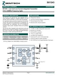
SX8725 - Semtech
SX8725 - Semtech
SX8725 - Semtech

Create successful ePaper yourself
Turn your PDF publications into a flip-book with our unique Google optimized e-Paper software.
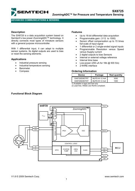
ADVANCED COMMUNICATIONS & SENSING<br />
<strong>SX8725</strong><br />
ZoomingADC for Pressure and Temperature Sensing<br />
Description<br />
The <strong>SX8725</strong> is a data acquisition system based on<br />
<strong>Semtech</strong>’s low power ZoomingADC technology. It<br />
directly connects most types of miniature sensors<br />
with a general purpose microcontroller.<br />
With 1 differential input, it can adapt to multiple<br />
sensor systems. Its digital outputs are used to bias<br />
or reset the sensing elements.<br />
Applications<br />
• Industrial pressure sensing<br />
• Industrial temperature sensing<br />
• Barometer<br />
• Compass<br />
Features<br />
• Up to 16-bit differential data acquisition<br />
• Programmable gain: (1/12 to 1000)<br />
• Sensor offset compensation up to 15 times<br />
full scale of input signal<br />
• 1 differential or 2 single-ended signal inputs<br />
• Programmable Resolution versus Speed<br />
versus Supply current<br />
• 2 digital outputs to bias Sensors<br />
• Internal or external voltage reference<br />
• Internal time base<br />
• Low-power (250 uA for 16b @ 500 S/s)<br />
• 2-WIRE interface<br />
Ordering Information<br />
Device Package Reel quantity<br />
<strong>SX8725</strong>E083TRT<br />
<strong>SX8725</strong>E083TDT<br />
MLPD-W-12 4x4<br />
MLPD-W-12 4x4<br />
1) Available in tape and reel only<br />
2) Lead free, WEEE and RoHS compliant.<br />
3000<br />
1000<br />
Functional Block Diagram<br />
V1.8 © 2009 <strong>Semtech</strong> Corp. www.semtech.com<br />
1
ADVANCED COMMUNICATIONS & SENSING<br />
<strong>SX8725</strong><br />
ZoomingADC for Pressure and Temperature Sensing<br />
Table of Contents<br />
Description..............................................................................................................................................................1<br />
Applications............................................................................................................................................................1<br />
Features ..................................................................................................................................................................1<br />
Ordering Information .............................................................................................................................................1<br />
Functional Block Diagram.....................................................................................................................................1<br />
Absolute Maximum Ratings ..................................................................................................................................4<br />
Electrical Characteristics ......................................................................................................................................5<br />
ZoomingADC Specifications.................................................................................................................................6<br />
Timing Characteristics ..........................................................................................................................................8<br />
2-WIRE Timing Waveforms ...................................................................................................................................8<br />
Pin Configuration ...................................................................................................................................................9<br />
Marking Information...............................................................................................................................................9<br />
Pin Description.......................................................................................................................................................9<br />
Circuit Description ...............................................................................................................................................10<br />
General Description .............................................................................................................................................. 10<br />
Block Diagram ....................................................................................................................................................... 10<br />
VREF..................................................................................................................................................................... 10<br />
GPIO ..................................................................................................................................................................... 11<br />
Charge Pump ........................................................................................................................................................ 12<br />
RC Oscillator ......................................................................................................................................................... 13<br />
2-WIRE.................................................................................................................................................................. 14<br />
2-WIRE Communication Format ........................................................................................................................... 14<br />
2-WIRE Address.................................................................................................................................................... 14<br />
ZoomingADC ........................................................................................................................................................15<br />
Features ................................................................................................................................................................ 15<br />
Overview ............................................................................................................................................................... 15<br />
ZADC Description.................................................................................................................................................. 15<br />
Acquisition Chain................................................................................................................................................... 15<br />
Registers ............................................................................................................................................................... 17<br />
ZADC Detailed Functionality Description.............................................................................................................. 18<br />
Continuous-Time vs. On-Request......................................................................................................................... 18<br />
Input Multiplexers .................................................................................................................................................. 19<br />
Programmable Gain Amplifiers ............................................................................................................................. 20<br />
PGA & ADC Enabling............................................................................................................................................ 21<br />
PGA1..................................................................................................................................................................... 21<br />
PGA2..................................................................................................................................................................... 21<br />
PGA3..................................................................................................................................................................... 21<br />
ADC Characteristics.............................................................................................................................................. 22<br />
Conversion Sequence........................................................................................................................................... 22<br />
Over-Sampling Frequency .................................................................................................................................... 22<br />
Over-Sampling Ratio............................................................................................................................................. 23<br />
Elementary Conversions ....................................................................................................................................... 23<br />
Resolution ............................................................................................................................................................. 24<br />
Conversion Time and Throughput......................................................................................................................... 25<br />
Output Code Format ............................................................................................................................................. 26<br />
Power Saving Modes ............................................................................................................................................ 27<br />
Registers Map ....................................................................................................................................................... 28<br />
Registers Descriptions .......................................................................................................................................... 28<br />
RC Register........................................................................................................................................................... 28<br />
GPIO Registers ..................................................................................................................................................... 29<br />
ZADC Registers .................................................................................................................................................... 30<br />
Mode Register ....................................................................................................................................................... 31<br />
Optional Operating Modes: External Voltage Reference Option .......................................................................... 32<br />
Application Hints..................................................................................................................................................33<br />
Recommended Operation Mode and Registers Settings...................................................................................... 33<br />
Operation Mode..................................................................................................................................................... 33<br />
V1.8 © 2009 <strong>Semtech</strong> Corp. www.semtech.com<br />
2
ADVANCED COMMUNICATIONS & SENSING<br />
<strong>SX8725</strong><br />
ZoomingADC for Pressure and Temperature Sensing<br />
Registers Settings ................................................................................................................................................. 33<br />
Schematic.............................................................................................................................................................. 34<br />
Input Impedance.................................................................................................................................................... 35<br />
Switched Capacitor Principle ................................................................................................................................ 36<br />
PGA Settling or Input Channel Modifications........................................................................................................ 37<br />
PGA Gain & Offset, Linearity and Noise ............................................................................................................... 37<br />
Frequency Response ............................................................................................................................................ 38<br />
Power Reduction................................................................................................................................................... 39<br />
Recommended Design for Other 2-WIRE Devices Connection ........................................................................... 39<br />
Typical Performance............................................................................................................................................40<br />
Linearity................................................................................................................................................................. 40<br />
Integral Non-Linearity............................................................................................................................................ 40<br />
Differential Non-Linearity....................................................................................................................................... 43<br />
Noise ..................................................................................................................................................................... 44<br />
Gain Error and Offset Error ................................................................................................................................... 46<br />
Power Consumption.............................................................................................................................................. 47<br />
PCB Layout Considerations................................................................................................................................49<br />
How to Evaluate....................................................................................................................................................49<br />
Package Outline Drawing: MLPD-W-12 4x4.......................................................................................................50<br />
Land Pattern Drawing: MLPD-W-12 4x4.............................................................................................................51<br />
Tape and Reel Specification ...............................................................................................................................52<br />
V1.8 © 2009 <strong>Semtech</strong> Corp. www.semtech.com<br />
3
ADVANCED COMMUNICATIONS & SENSING<br />
<strong>SX8725</strong><br />
ZoomingADC for Pressure and Temperature Sensing<br />
Absolute Maximum Ratings<br />
Exceeding the specifications below may result in permanent damage to the device or device malfunction.<br />
Operation outside the parameters specified in the Electrical Characteristics section is not implied.<br />
Parameter Symbol Comments / Conditions Min Max Unit<br />
Power supply V BATT V SS - 0.3 5.7 V<br />
Storage temperature T STORE -55 150 °C<br />
Temperature under bias T BIAS -40 140 °C<br />
Max sensor common mode<br />
V VR_P<br />
V SS - 300 V BATT + 300 mV<br />
V VR_N<br />
Input voltage V SS - 300 V BATT + 300 mV<br />
Peak reflow temperature T PKG 260 °C<br />
Notes: This device is ESD sensitive. Use of standard ESD handling precautions is required.<br />
V1.8 © 2009 <strong>Semtech</strong> Corp. www.semtech.com<br />
4
ADVANCED COMMUNICATIONS & SENSING<br />
<strong>SX8725</strong><br />
ZoomingADC for Pressure and Temperature Sensing<br />
Electrical Characteristics<br />
All values are valid within the operating conditions unless otherwise specified.<br />
Parameter Symbol Comments / Conditions Min Typ Max Unit<br />
Operating conditions<br />
Power supply V BATT 2.4 5.5 V<br />
Operating temperature T OP -40 125 ° C<br />
Current consumption<br />
Active current, @ 30 °C, 5.5 V<br />
Active current, @ 30 °C, 3.3 V<br />
Sleep current<br />
Time base<br />
I OP<br />
I OP<br />
I sleep<br />
16 b @ 250 Sample/s<br />
ADC, f s = 125 kHz<br />
16 b @ 1 kSample/s<br />
PGA3 + ADC, f s= 500 kHz<br />
16 b + gain 1000 @ 1 kSample/s<br />
PGA3,2,1 + ADC, f s = 500kHz<br />
16 b @ 250 Sample/s<br />
PGA3 + ADC, f s = 125 kHz<br />
16 b @ 1 kSample/s<br />
PGA3 + ADC, f s= 500 kHz<br />
16 b + gain 1000 @ 1 kSample/s<br />
PGA3,2,1 + ADC, f s = 500kHz<br />
250 300<br />
700 800<br />
1000 1200<br />
150<br />
300<br />
850<br />
@ 30 °C 75 200<br />
up to 85 °C 100<br />
@125 °C 150<br />
Max ADC over-sampling frequency F Smax @ 25 °C 450 500 550 kHz<br />
Min ADC over-sampling frequency F Smin @ 25 °C 56.25 62.5 68.75 kHz<br />
Digital I/O<br />
Input logic high V IH 0.7 V BATT<br />
Input logic low V IL 0.3 V BATT<br />
Output logic high V OH I OH < 4mA V BATT-0.4 V<br />
Output logic low V OL I OL < 4mA 0.4 V<br />
VREF: Internal Bandgap Reference<br />
Absolute output voltage V BATT > 3V 1.19 1.22 1.25 V<br />
Variation over Temperature V BATT > 3V, ref to 25° C -1 +1 %<br />
Total Output Noise V BATT > 3V, rms, broadband 1 mV<br />
µA<br />
µA<br />
nA<br />
V1.8 © 2009 <strong>Semtech</strong> Corp. www.semtech.com<br />
5
ADVANCED COMMUNICATIONS & SENSING<br />
<strong>SX8725</strong><br />
ZoomingADC for Pressure and Temperature Sensing<br />
ZoomingADC Specifications<br />
Unless otherwise specified: Temperature T A = +25° C, V DD = +5V, GND = 0V, V REF, ADC = +5V, V IN = 0V, over-sampling frequency<br />
f S = 250 kHz, PGA3 on with Gain = 1, PGA1&PGA2 off, offsets GDOff 2 = GDOff 3 = 0. Power operation: normal (IB_AMP_ADC[1:0] =<br />
IB_AMP_PGA[1:0] = '01'). For resolution n = 12 bits: OSR = 32 and N ELCONV = 4. For resolution n = 16 bits: OSR = 512 and N ELCONV = 2.<br />
Bandgap chopped at N ELCONV rate.<br />
Parameter Symbol Comments / Conditions Min Typ Max Unit<br />
Analog Input<br />
Differential Input Voltage Ranges<br />
V IN = (V INP - V INN)<br />
Reference Voltage Range<br />
V REF, ADC = (V REFP – V REFN)<br />
Programmable Gain Amplifier (PGA)<br />
Gain = 1, OSR = 32 (Note 1) -2.42 2.42 V<br />
Gain = 100, OSR = 32 -24.2 24.2 mV<br />
Gain = 1000, OSR = 32 -2.42 2.42 mV<br />
Total PGA Gain GD TOT (Note 1) 1/12 1000 V/V<br />
PGA1 Gain GD 1 See Table 5 1 10 V/V<br />
PGA2 Gain GD 2 See Table 6 1 10 V/V<br />
PGA3 Gain GD 3 Step = 1/12 V/V, See Table 8 0 127/12 V/V<br />
Gain Setting Precision (each stage) -3 ±0.5 3 %<br />
Gain Temperature Dependence ±5 ppm/°C<br />
PGA2 Offset GDoff 2 Step = 0.2 V/V, See Table 7 -1 1 V/V<br />
PGA3 Offset GDoff 3 Step = 1/12 V/V, See Table 9 -63/12 63/12 V/V<br />
Offset Setting Precision (PGA2 or 3) (Note 2) -3 ±0.5 3 %<br />
Offset Temperature Dependence ±5 ppm/°C<br />
Input Impedance PGA1<br />
Gain = 1 (Note 3) 1500 kΩ<br />
Gain = 10 (Note 3) 150 kΩ<br />
Input Impedance PGA2, PGA3 Maximal gain (Note 3) 150 kΩ<br />
Output RMS noise<br />
ADC Static Performance<br />
PGA1 (Note 4) 205 µV<br />
PGA2 (Note 5) 340 µV<br />
PGA3 (Note 6) 365 µV<br />
Resolution, n (Note 7) 6 16 Bits<br />
No Missing Codes (Note 8) 16 Bits<br />
Gain Error (Note 9) ±0.15 %<br />
Offset Error n = 16 bits (Note 10)<br />
Integral Non-Linearity, INL<br />
Differential Non-Linearity, DNL<br />
V1.8 © 2009 <strong>Semtech</strong> Corp. www.semtech.com<br />
6<br />
V DD<br />
V<br />
±1 %<br />
±1 LSB<br />
n = 12 Bits (Note 11) ±0.6 LSB<br />
n = 16 Bits (Note 11) ±1.5 LSB<br />
n = 12 Bits (Note 12) ±0.5 LSB<br />
n = 16 Bits (Note 12) ±0.5 LSB<br />
Common Mode input range V SS-0.3 V BATT+0.3 V<br />
Power Supply Rejection Ratio<br />
ADC Dynamic Performance<br />
Conversion Time<br />
Throughput Rate (Continuous Mode)<br />
PSRR<br />
T CONV<br />
1/T CONV<br />
VDD = 5V ± 0.3V (Note 13) 78 dB<br />
VDD = 3V ± 0.3V (Note 13) 72 dB<br />
n = 12 bits (Note 14) 133 cycles/f S<br />
n = 16 bits (Note 14) 1027 cycles/f S<br />
n = 12 bits, f S = 250kHz 1.88 kSps<br />
n = 16 bits, f S = 250kHz 0.485 kSps<br />
Nbr of Initialization Cycles N INIT 0 2 cycles
ADVANCED COMMUNICATIONS & SENSING<br />
<strong>SX8725</strong><br />
ZoomingADC for Pressure and Temperature Sensing<br />
Parameter Symbol Comments / Conditions Min Typ Max Unit<br />
Nbr of End Conversion Cycles N END 0 5 cycles<br />
PGA Stabilization Delay (Note 15) OSR cycles<br />
ADC Digital Output<br />
Output Data Coding<br />
Power Supply<br />
Binary Two’s Complement<br />
See Table 15 and Table 16<br />
Voltage Supply Range V DD 2.4 5 5.5 V<br />
Analog Quiescent Current<br />
Only ZoomingADC<br />
Total Consumption I Q V DD = 5V/3V 800/675 µA<br />
ADC Only Consumption V DD = 5V/3V 260/190 µA<br />
PGA1 Consumption V DD = 5V/3V 190/170 µA<br />
PGA2 Consumption V DD = 5V/3V 150/135 µA<br />
PGA3 Consumption V DD = 5V/3V 200/180 µA<br />
Analog Power Dissipation<br />
All PGAs & ADC Active<br />
Normal Power Mode V DD = 5V/3V (Note 16) 4.0/2.0 mW<br />
3/4 Power Reduction Mode V DD = 5V/3V (Note 17) 3.2/1.6 mW<br />
1/2 Power Reduction Mode V DD = 5V/3V (Note 18) 2.4/1.1 mW<br />
1/4 Power Reduction Mode V DD = 5V/3V (Note 19) 1.5/0.7 mW<br />
Temperature<br />
Operating Range -40 125 °C<br />
Notes:<br />
(1) Gain defined as overall PGA gain GD TOT = GD 1⋅GD 2⋅GD 3. Maximum input voltage is given by:<br />
V IN, MAX = ±(V REF,ADC/2)⋅(OSR/OSR+1).<br />
(2) Offset due to tolerance on GDoff 2 or GDoff 3 setting. For small intrinsic offset, use only ADC and PGA1.<br />
(3) Measured with block connected to inputs through AMUX block. Normalized input sampling frequency for input impedance is f S =<br />
500kHz. This figure must be multiplied by 2 for f S = 250kHz, 4 for f S = 125kHz. Input impedance is proportional to 1/ f S.<br />
(4) Figure independent on PGA1 gain and sampling frequency f S.<br />
(5) Figure independent on PGA2 gain and sampling frequency f S.<br />
(6) Figure independent on PGA3 gain and sampling frequency f S.<br />
(7) Resolution is given by n = 2⋅log2(OSR) + log2(N ELCONV). OSR can be set between 8 and 1024, in powers of 2. N ELCONV can be set to 1,<br />
2, 4 or 8.<br />
(8) If a ramp signal is applied to the input, all digital codes appear in the resulting ADC output data.<br />
(9) Gain error is defined as the amount of deviation between the ideal (theoretical) transfer function and the measured transfer function<br />
(with the offset error removed).<br />
(10) Offset error is defined as the output code error for a zero volt input (ideally, output code = 0). For ± 1 LSB offset, N ELCONV must be ≥2.<br />
(11) INL defined as the deviation of the DC transfer curve of each individual code from the best-fit straight line. This specification holds<br />
over the full scale. (For 16 bits INL set PGA3 on).<br />
(12) DNL is defined as the difference (in LSB) between the ideal (1 LSB) and measured code transitions for successive codes.<br />
(13) Figures for Gains = 1 to 100. PSRR is defined as the amount of change in the ADC output value as the power supply voltage<br />
changes.<br />
(14) Conversion time is given by: T CONV = (N ELCONV ⋅ (OSR + 1) + 1) / f S. OSR can be set between 8 and 1024, in powers of 2. N ELCONV can<br />
be set to 1, 2, 4 or 8.<br />
(15) PGAs are reset after each writing operation to registers RegACCfg1-5. The ADC must be started after a PGA or inputs commonmode<br />
stabilization delay. This is done by writing bit Start several cycles after PGA settings modification or channel switching. Delay<br />
between PGA start or input channel switching and ADC start should be equivalent to OSR (between 8 and 1024) number of cycles.<br />
This delay does not apply to conversions made without the PGAs.<br />
(16) Nominal (maximum) bias currents in PGAs and ADC, i.e. IB_AMP_PGA[1:0] = '11' and IB_AMP_ADC[1:0] = '11'.<br />
(17) Bias currents in PGAs and ADC set to 3/4 of nominal values, i.e. IB_AMP_PGA[1:0] = '10', IB_AMP_ADC[1:0] = '10'.<br />
(18) Bias currents in PGAs and ADC set to 1/2 of nominal values, i.e. IB_AMP_PGA[1:0] = '01', IB_AMP_ADC[1:0] = '01'.<br />
(19) Bias currents in PGAs and ADC set to 1/4 of nominal values, i.e. IB_AMP_PGA[1:0] = '00', IB_AMP_ADC[1:0] = '00'.<br />
V1.8 © 2009 <strong>Semtech</strong> Corp. www.semtech.com<br />
7
ADVANCED COMMUNICATIONS & SENSING<br />
<strong>SX8725</strong><br />
ZoomingADC for Pressure and Temperature Sensing<br />
Timing Characteristics<br />
Parameter Symbol Comments / Conditions Min Typ Max Unit<br />
Interrupt (Ready) timing specification<br />
READY pulse width (2) t IRQ 1 1/F S<br />
2-WIRE timing specifications(1)<br />
SCL clock frequency f SCL 0 400 kHz<br />
SCL low period t LOW 1.3 µs<br />
SCL high period t HIGH 0.6 µs<br />
Data setup time t SU;DAT 100 ns<br />
Data hold time t HD;DAT 0 ns<br />
Repeated start setup time t SU;STA 0.6 µs<br />
Start condition hold time t HD;STA 0.6 µs<br />
Stop condition hold time t SU;STO 0.6 µs<br />
Bus free time between stop and start t BUF 1.3 µs<br />
Input glitch suppression t SP 50 ns<br />
Notes:<br />
(1) All timing specifications are referred to VILmin and VIHmax voltage levels defined for the SCL and SDA pins.<br />
(2) The READY pulse indicates End of Conversion. This is a Low going pulse of duration equal to one cycle of the ADC sampling rate.<br />
2-WIRE Timing Waveforms<br />
SDA<br />
SCL<br />
t SU;STA<br />
t HD;STA<br />
t SU;STO<br />
t BUF<br />
Figure 1 - 2-WIRE Start and Stop timings<br />
SDA<br />
SCL<br />
t LOW<br />
t HIGH<br />
t HD;DAT<br />
t SU;DAT<br />
t SP<br />
Figure 2 - 2-WIRE Data timings<br />
V1.8 © 2009 <strong>Semtech</strong> Corp. www.semtech.com<br />
8
ADVANCED COMMUNICATIONS & SENSING<br />
<strong>SX8725</strong><br />
ZoomingADC for Pressure and Temperature Sensing<br />
Pin Configuration<br />
Marking Information<br />
8725<br />
yyww<br />
xxxxx<br />
xxxxx<br />
yyww = Date code<br />
xxxx = <strong>Semtech</strong> lot number<br />
Pin Description<br />
Pin Name Type Function<br />
1 NC - Not Connected<br />
2 NC - Not Connected<br />
3 V BATT Power Input 2.4V to 5.5V power supply<br />
4 V SS Power Input Chip Ground<br />
5 READY Digital Output Conversion complete flag.<br />
6 D 1 Digital IO + analog<br />
7 D 0 Digital IO + analog<br />
8 SDA Digital IO 2-WIRE Data<br />
Digital output sensor drive (V BATT or V SS)<br />
V REF Input in optional operating mode<br />
Digital output sensor drive (V BATT or V SS)<br />
V REF Output in optional operating mode<br />
9 SCL Digital IO 2-WIRE Clock. Up to 400KHz.<br />
10 V PUMP Power IO<br />
Charge pump output. Raises ADC supply above V BATT if V BATT supply is too low.<br />
Recommended range for capacitor is 1nF to 10 nF. Connect the capacitor to GND.<br />
11 AC 2 Analog Input Differential sensor input in conjunction with AC 3<br />
12 AC 3 Analog Input Differential sensor input in conjunction with AC 2<br />
13 V SS Power Input Bottom ground pad (1)<br />
Notes:<br />
(1) This pin is internally connected to V SS. It should also be connected to V SS on PCB to reduce noise and improve thermal behavior.<br />
V1.8 © 2009 <strong>Semtech</strong> Corp. www.semtech.com<br />
9
ADVANCED COMMUNICATIONS & SENSING<br />
<strong>SX8725</strong><br />
ZoomingADC for Pressure and Temperature Sensing<br />
Circuit Description<br />
General Description<br />
The <strong>SX8725</strong> is a complete low-power acquisition path with programmable gain, acquisition speed and<br />
resolution.<br />
Block Diagram<br />
<strong>SX8725</strong><br />
V REF<br />
+<br />
-<br />
+<br />
-<br />
+<br />
-<br />
REF MUX<br />
ZoomingADC TM<br />
V BATT<br />
AC0<br />
AC1<br />
AC2<br />
AC3<br />
SIGNAL MUX<br />
PGA<br />
ADC<br />
READY<br />
CONTROL LOGIC<br />
D0/REF OUT<br />
D1/REF IN<br />
GPIO<br />
CHARGE<br />
PUMP<br />
4MHz<br />
OSC<br />
I 2 C<br />
SCL<br />
SDA<br />
V PUMP<br />
VSS<br />
Figure 3 - <strong>SX8725</strong> Block Diagram<br />
VREF<br />
The internally generated V REF is a trimmed bandgap reference with a nominal value of 1.22V that provides a<br />
stable voltage reference for the ZoomingADC.<br />
This reference voltage is directly connected to one of the ZoomingADC reference multiplexer inputs.<br />
The bandgap voltage stability is only guaranteed for V BATT voltages of 3V and above. As V BATT drops down to<br />
2.4V, the bandgap voltage could reduce by up to 50mV.<br />
The bandgap has relatively weak output drive so it is recommended that if the bandgap is required as a signal<br />
input then PGA1 must be enabled with Gain = 1.<br />
V1.8 © 2009 <strong>Semtech</strong> Corp. www.semtech.com<br />
10
ADVANCED COMMUNICATIONS & SENSING<br />
<strong>SX8725</strong><br />
ZoomingADC for Pressure and Temperature Sensing<br />
GPIO<br />
The GPIO block is a multipurpose 4 bit input/output port. In addition to digital behavior, D0 and D1 pins can be<br />
programmed as analog pins in order to be used as output (reference voltage monitoring) and input for an<br />
external reference voltage (For further details see Figure 14, Figure 15, Figure 16 and Figure 17). Each port<br />
terminal can be individually selected as digital input or output.<br />
RegOut[4]<br />
RegOut[0]<br />
D0/REF OUT<br />
0<br />
1<br />
RegIn[0]<br />
RegMode[1]<br />
V REF<br />
+<br />
-<br />
0<br />
1<br />
ZoomingADC<br />
RegMode[0]<br />
RegOut[5]<br />
D1/REF IN<br />
1<br />
0<br />
RegOut[1]<br />
RegIn[1]<br />
Figure 4 - GPIO Block Diagram<br />
The direction of each bit within the GPIO block (input only or input/output) can be individually set using the 4 th<br />
and 5 th bits of the RegOut register. If D[x]_DIR = 1, both the input and output buffer are active on the<br />
corresponding GPIO block pin. If D[x]_DIR = 0, the corresponding GPIO block pin is an input only and the<br />
output buffer is in high impedance. After power on reset the GPIO block pins are in input/output mode<br />
(D[x]_DIR are reset to 1)<br />
The input values of GPIO block are available in RegIn register (read only). Reading is always direct – there is<br />
no debounce function in the GPIO block. In case of possible noise on input signals, an external hardware filter<br />
has to be realized. The input buffer is also active when the GPIO block is defined as output and the effective<br />
value on the pin can be read back.<br />
Data stored in the 1 st and 2 nd bits of RegOut register are outputted at GPIO block if D[x]_DIR = 1. The default<br />
values after power on reset is low (0).<br />
The digital pins are able to deliver a driving current up to 8 mA.<br />
When the bits VREF_D0_OUT and VREF_D1_IN in the RegMode register are set to 1 the D0 and D1 pins<br />
digital behavior are automatically bypassed in order to either input or output the voltage reference signals.<br />
V1.8 © 2009 <strong>Semtech</strong> Corp. www.semtech.com<br />
11
ADVANCED COMMUNICATIONS & SENSING<br />
<strong>SX8725</strong><br />
ZoomingADC for Pressure and Temperature Sensing<br />
Charge Pump<br />
This block generates a supply voltage able to power the analog switch drive levels on the chip.<br />
The minimum acceptable switch supply is 3V which means that if V BATT drops below 3V then the block should<br />
be activated to generate a voltage of 3V or above. If V BATT is greater than 3V then V BATT may be switched<br />
straight through to the V PUMP output.<br />
If control input bit MULT_FORCE_OFF = 1 in RegMode register then the charge pump is disabled and V BATT is<br />
permanently connected to V PUMP .<br />
If control input bit MULT_FORCE_ON = 1 in RegMode register then the charge pump is permanently enabled.<br />
This overrides MULT_FORCE_OFF bit in RegMode register.<br />
If MULT_FORCE_ON = 0 and MULT_FORCE_OFF = 0 bits in RegMode register then the charge pump will<br />
start if V BATT drops below 3V, otherwise V BATT will be switched directly through to V PUMP .<br />
These controls are supplied to give the user the option of fixing the charge pump state to avoid it turning off and<br />
on when V BATT is close to 3V.<br />
The cell will use the on-chip bandgap reference and comparator to detect when V BATT is too low. When<br />
activated, the block will use the charge pump to boost the V BATT voltage to above 3V but with diode limiting to<br />
ensure that the generated voltage never exceeds 0.7V above V BATT .<br />
An external capacitor is required on V PUMP whenever the power supply is supposed to be less or drop below 3V.<br />
This capacitor should be large enough to ensure that generated voltage is smooth enough to avoid affecting<br />
conversion accuracy but not so large that it gives an unacceptable settling time. A recommended value is<br />
around 2.2nF.<br />
The block will also indicate when the pumped output voltage is sufficiently high to allow ADC conversions to be<br />
started. This will be a simple comparison which will give a ready signal when the V PUMP output is 3V or above.<br />
V1.8 © 2009 <strong>Semtech</strong> Corp. www.semtech.com<br />
12
ADVANCED COMMUNICATIONS & SENSING<br />
<strong>SX8725</strong><br />
ZoomingADC for Pressure and Temperature Sensing<br />
RC Oscillator<br />
This block provides the master clock reference for the chip. It produces a clock at 4 MHz which is divided<br />
internally in order to generate the clock sources needed by the other blocks.<br />
The oscillator technique is a low power relaxation design and it is designed to vary as little as possible over<br />
temperature and supply voltage.<br />
This oscillator is trimmed at manufacture chip test.<br />
The RC oscillator will start up after a chip reset to allow the trimming values to be read and calibration registers<br />
and 2-WIRE address set to their programmed values. Once this has been done, the oscillator will be shut down<br />
and the chip will enter a sleep state while waiting for an 2-WIRE communication.<br />
V1.8 © 2009 <strong>Semtech</strong> Corp. www.semtech.com<br />
13
ADVANCED COMMUNICATIONS & SENSING<br />
<strong>SX8725</strong><br />
ZoomingADC for Pressure and Temperature Sensing<br />
2-WIRE<br />
The 2-WIRE interface gives access to the chip registers. It complies with the 2-WIRE protocol specifications,<br />
restricted to the slave side of the communication.<br />
General features:<br />
• Slave only operation<br />
• Fast mode operation (up to 400 kHz)<br />
• Combined read and write mode support<br />
• General call reset support<br />
• 7-bit device address customization<br />
• Stretch 2-WIRE clock SCL only before sending ACK/NACK<br />
The interface handles 2-WIRE communication at the transaction level: the processor is only aware of read and<br />
writes transactions. A read transaction is an external request to get the content of system memory location and<br />
a write transaction is an external request to write the content of a system memory location.<br />
2-WIRE Communication Format<br />
Start Slave Address ACK W Memory Address ACK Start Slave Address ACK R Data NACK Stop<br />
SDA<br />
1 0 0 1 0 0 0 0 0<br />
1 0 0 1 0 0 0 1<br />
A7 A6 A5 A4 A3 A2 A1 A0 D7 D6 D5 D4 D3 D2 D1 D0<br />
SCL<br />
1 9 1 9 1 9 1 9<br />
Master <strong>SX8725</strong><br />
Master <strong>SX8725</strong><br />
Master <strong>SX8725</strong><br />
Master<br />
Figure 5 - Timing Diagram for Reading from <strong>SX8725</strong><br />
Start Slave Address ACK W Memory Address ACK Start Slave Address ACK W Data ACK Stop<br />
SDA<br />
1 0 0 1 0 0 0 0<br />
1 0 0 1 0 0 0 0 0 A7 A6 A5 A4 A3 A2 A1 A0 D7 D6 D5 D4 D3 D2 D1 D0<br />
SCL<br />
1 9 1 9 1 9 1 9<br />
Master <strong>SX8725</strong> Master <strong>SX8725</strong><br />
Master <strong>SX8725</strong><br />
Master<br />
Figure 6 - Timing Diagram for Writing to the <strong>SX8725</strong><br />
<strong>SX8725</strong><br />
Master<br />
Start Slave Address ACK W RegACOutMsb ACK Start Slave Address ACK R Data NACK Stop<br />
SDA<br />
1 0 0 1 0 0 0 0 0<br />
1 1 0 0 0 0 1<br />
1 0 0 1 0 0 0 1<br />
0 D7 D6 D5 D4 D3 D2 D1 D0<br />
...<br />
SCL<br />
...<br />
Ready<br />
1 9 1 9 1 9 1 9<br />
Master <strong>SX8725</strong><br />
Master <strong>SX8725</strong><br />
Master <strong>SX8725</strong><br />
Master<br />
Start Slave Address ACK W RegACOutLsb ACK Start Slave Address ACK R Data NACK Stop<br />
SDA ...<br />
SCL ...<br />
1 0 0 1 0 0 0 0 0<br />
1 1 0 0 0 0 0<br />
1 0 0 1 0 0 0 1<br />
0 D7 D6 D5 D4 D3 D2 D1 D0<br />
Ready<br />
1 9 1 9 1 9 1 9<br />
2-WIRE Address<br />
Master <strong>SX8725</strong><br />
Master <strong>SX8725</strong><br />
Master <strong>SX8725</strong><br />
Master<br />
Figure 7 - Timing Diagram for Reading an ADC Sample from <strong>SX8725</strong><br />
The default 2-WIRE slave address is 1001000 in binary.<br />
This is the standard part 2-WIRE slave address. Other addresses between 1001001 and 1001111 are available<br />
by special request.<br />
V1.8 © 2009 <strong>Semtech</strong> Corp. www.semtech.com<br />
14
ADVANCED COMMUNICATIONS & SENSING<br />
<strong>SX8725</strong><br />
ZoomingADC for Pressure and Temperature Sensing<br />
ZoomingADC<br />
Features<br />
The ZoomingADC is a complete and versatile low-power analog front-end interface typically intended for sensing<br />
applications.<br />
In the following text the ZoomingADC will be referred as ZADC.<br />
The key features of the ZADC are:<br />
• Programmable 6 to 16-bit dynamic range over-sampled ADC<br />
• Flexible gain programming between 0.5 and 1000<br />
• Flexible and large range offset compensation<br />
• 2-channel differential or 3-channel single-ended input<br />
• 2-channel differential reference inputs<br />
• Power saving modes<br />
Overview<br />
Analog<br />
Inputs<br />
Reference<br />
Inputs<br />
V SS<br />
V REF<br />
AC 0<br />
AC 1<br />
AC 2<br />
AC 3<br />
V BATT<br />
+<br />
V SS -<br />
V REF +<br />
V SS<br />
Figure 8 - ZADC General Functional Block Diagram<br />
The total acquisition chain consists of an input multiplexer, 3 programmable gain amplifier stages and an over<br />
sampled A/D converter. The reference voltage can be selected on two different channels. Two offset compensation<br />
amplifiers allow for a wide offset compensation range. The programmable gain and offset allow the application to<br />
zoom in on a small portion of the reference voltage defined input range.<br />
ZADC Description<br />
Acquisition Chain<br />
Input<br />
Selection<br />
-<br />
Reference<br />
Selection<br />
f s<br />
PGA1 PGA2 PGA3<br />
V IN<br />
V D1<br />
V D2<br />
V IN,ADC<br />
+<br />
+<br />
GD1<br />
GD2<br />
GD3<br />
-<br />
-<br />
OFF2<br />
OFF3<br />
V REF,ADC<br />
Gain 1 Gain 2 Offset 2 Gain 3 Offset 3<br />
ZOOM<br />
Figure 8 shows the general block diagram of the acquisition chain (AC). A control block (not shown in Figure 8)<br />
manages all communications with the 2-WIRE peripheral. The clocking is derived from the internal 4 MHz<br />
Oscillator.<br />
Analog inputs can be selected through a 4 input multiplexer, while reference input is selected between two differential<br />
channels. It should however be noted that only 3 acquisition channels (including the V REF ) are available when<br />
configured as single ended since the input amplifier is always operating in differential mode with both positive and<br />
negative input selected through the multiplexer.<br />
The core of the zooming section is made of three differential programmable amplifiers (PGA). After selection of an<br />
input and reference signals V IN and V REF,ADC combination, the input voltage is modulated and amplified through<br />
f s<br />
ADC<br />
16<br />
V1.8 © 2009 <strong>Semtech</strong> Corp. www.semtech.com<br />
15
ADVANCED COMMUNICATIONS & SENSING<br />
<strong>SX8725</strong><br />
ZoomingADC for Pressure and Temperature Sensing<br />
stages 1 to 3. Fine gain programming up to 1'000 V/V is possible. In addition, the last two stages provide<br />
programmable offset. Each amplifier can be bypassed if needed.<br />
The output of the PGA stages is directly fed to the analog-to-digital converter (ADC), which converts the signal<br />
V IN,ADC into digital.<br />
Like most ADCs intended for instrumentation or sensing applications, the ZoomingADC is an over-sampled<br />
converter (See Note 1 ). The ADC is a so-called incremental converter; with bipolar operation (the ADC accepts<br />
both positive and negative differential input voltages). In first approximation, the ADC output result relative to<br />
full-scale (FS) delivers the quantity:<br />
OUT V<br />
ADC IN<br />
≅<br />
FS<br />
/ 2 VREF<br />
,<br />
Equation 1<br />
in two's complement (see Equation 4 and Equation 5 for details). The output code OUT ADC is -FS/2 to +FS/2 for<br />
V IN,ADC ≅ -V REF,ADC /2 to +V REF,ADC /2 respectively. As will be shown, V IN,ADC is related to input voltage V IN by the<br />
relationship:<br />
, ADC<br />
ADC<br />
/ 2<br />
V<br />
IN , ADC<br />
GDTOT<br />
⋅VIN<br />
− GDoffTOT<br />
⋅VREF<br />
, ADC<br />
= (V)<br />
Equation 2<br />
where GD TOT is the total PGA gain, and GDoff TOT is the total PGA offset.<br />
1 Note: Over-sampled converters are operated with a sampling frequency f S much higher than the input signal's Nyquist rate (typically f S is<br />
20-1'000 times the input signal bandwidth). The sampling frequency to throughput ratio is large (typically 10-500). These converters include<br />
digital decimation filtering. They are mainly used for high resolution, and/or low-to-medium speed applications.<br />
V1.8 © 2009 <strong>Semtech</strong> Corp. www.semtech.com<br />
16
ADVANCED COMMUNICATIONS & SENSING<br />
<strong>SX8725</strong><br />
ZoomingADC for Pressure and Temperature Sensing<br />
Registers<br />
The system has a bank of eight 8-bit registers: six registers are used to configure the acquisition chain<br />
(RegAcCfg0 to 5), and two registers are used to store the output code of the analog-to-digital conversion<br />
(RegAcOutMsb & Lsb).<br />
Register Name<br />
RegACOutLsb<br />
RegACOutMsb<br />
Bit Position<br />
7 6 5 4 3 2 1 0<br />
OUT[7:0]<br />
OUT[15:8]<br />
RegACCfg0<br />
Default values:<br />
START<br />
0<br />
SET_NELC[1:0]<br />
01<br />
SET_OSR[2:0]<br />
010<br />
CONT<br />
0<br />
-<br />
0<br />
RegACCfg1<br />
Default values:<br />
IB_AMP_ADC[1:0]<br />
11<br />
IB_AMP_PGA[1:0]<br />
11<br />
ENABLE[3:0]<br />
0000<br />
RegACCfg2<br />
Default values:<br />
FIN[1:0]<br />
00<br />
PGA2_GAIN[1:0]<br />
00<br />
PGA2_OFFSET[3:0]<br />
0000<br />
RegACCfg3<br />
Default values:<br />
PGA1_G<br />
0<br />
PGA3_GAIN[6:0]<br />
0001100<br />
RegACCfg4<br />
Default values:<br />
-<br />
0<br />
PGA3_OFFSET[6:0]<br />
0000000<br />
RegACCfg5<br />
Default values:<br />
BUSY<br />
0<br />
DEF<br />
0<br />
AMUX[4:0]<br />
00000<br />
VMUX<br />
0<br />
Table 1 - Peripheral Registers to Configure the Acquisition Chain (AC)<br />
and to Store the Analog-to-Digital Conversion (ADC) Result<br />
With:<br />
• OUT: (r) digital output code of the analog-to-digital converter. (MSB = OUT[15])<br />
• START: (w) setting this bit triggers a single conversion (after the current one is finished). This bit always reads back 0.<br />
• SET_NELC: (rw) sets the number of elementary conversions to 2 SET_NELC[1:0]. To compensate for offsets, the input signal is<br />
chopped between elementary conversions (1,2,4,8).<br />
• SET_OSR: (rw) sets the over-sampling rate (OSR) of an elementary conversion to 2(3+SET_OSR[2:0]). OSR = 8, 16, 32, ..., 512,<br />
1024.<br />
• CONT: (rw) setting this bit starts a conversion. A new conversion will automatically begin as long as the bit remains at 1.<br />
• TEST: bit only used for test purposes. In normal mode, this bit is forced to 0 and cannot be overwritten.<br />
• IB_AMP_ADC: (rw) sets the bias current in the ADC to 0.25*(1+ IB_AMP_ADC[1:0]) of the normal operation current (25, 50, 75 or<br />
100% of nominal current). To be used for low-power, low-speed operation.<br />
• IB_AMP_PGA: (rw) sets the bias current in the PGAs to 0.25*(1+IB_AMP_PGA[1:0]) of the normal operation current (25, 50, 75 or<br />
100% of nominal current). To be used for low-power, low-speed operation.<br />
• ENABLE: (rw) enables the ADC modulator (bit 0) and the different stages of the PGAs (PGAi by bit i=1,2,3). PGA stages that are<br />
disabled are bypassed.<br />
• FIN: (rw) These bits set the over sampling frequency of the acquisition chain. Expressed as a fraction of the oscillator frequency,<br />
the sampling frequency is given as: 11 500 kHz, 10 250 kHz, 01 125 kHz, 00 62.5 kHz.<br />
• PGA1_GAIN: (rw) sets the gain of the first stage: 0 1, 1 10.<br />
• PGA2_GAIN: (rw) sets the gain of the second stage: 00 1, 01 2, 10 5, 11 10.<br />
• PGA3_GAIN: (rw) sets the gain of the third stage to PGA3_GAIN[6:0]⋅1/12.<br />
• PGA2_OFFSET: (rw) sets the offset of the second stage between –1 and +1, with increments of 0.2. The MSB gives the sign<br />
(0 → positive, 1 → negative); amplitude is coded with the bits PGA2_OFFSET[5:0].<br />
• PGA3_OFFSET: (rw) sets the offset of the third stage between –5.25 and +5.25, with increments of 1/12. The MSB gives the sign<br />
(0 → positive, 1 → negative); amplitude is coded with the bits PGA3_OFFSET[5:0].<br />
• BUSY: (r) set to 1 if a conversion is running.<br />
• DEF: (w) sets all values to their defaults (PGA disabled, max speed, nominal modulator bias current, 2 elementary conversions,<br />
over-sampling rate of 32) and starts a new conversion without waiting the end of the preceding one.<br />
• AMUX(4:0): (rw) AMUX(4) sets the mode (0 differential inputs, 1 single ended inputs with A 0 = common reference) AMUX(3)<br />
sets the sign (0 straight, 1 cross) AMUX(2:0) sets the channel.<br />
• VMUX: (rw) sets the differential reference channel (0 V BATT, 1 V REF).<br />
(r = read; w = write; rw = read & write)<br />
V1.8 © 2009 <strong>Semtech</strong> Corp. www.semtech.com<br />
17
ADVANCED COMMUNICATIONS & SENSING<br />
<strong>SX8725</strong><br />
ZoomingADC for Pressure and Temperature Sensing<br />
ZADC Detailed Functionality Description<br />
Continuous-Time vs. On-Request<br />
The ADC can be operated in two distinct modes: "continuous-time" and "on-request" modes (selected using the<br />
bit CONT).<br />
In "continuous-time" mode, the input signal is repeatedly converted into digital. After a conversion is finished, a<br />
new one is automatically initiated. The new value is then written in the result register, and the corresponding<br />
internal trigger pulse is generated. This operation is sketched in Figure 9. The conversion time in this case is<br />
defined as T CONV .<br />
T CONV<br />
Internal Trig<br />
Output Code<br />
RegACOut[15:0]<br />
BUSY<br />
IRQ/READY<br />
Figure 9 - ADC "Continuous-Time" Operation<br />
In the "on-request" mode, the internal behavior of the converter is the same as in the "continuous-time" mode,<br />
but the conversion is initiated on user request (with the START bit). As shown in Figure 10, the conversion time<br />
is also T CONV .<br />
Figure 10 - ADC "On-Request" Operation<br />
V1.8 © 2009 <strong>Semtech</strong> Corp. www.semtech.com<br />
18
ADVANCED COMMUNICATIONS & SENSING<br />
<strong>SX8725</strong><br />
ZoomingADC for Pressure and Temperature Sensing<br />
Input Multiplexers<br />
The ZoomingADC has eight analog inputs AC 0 to AC 7 and four reference inputs AC_R 0 to AC_R 3 . Let us first<br />
define the differential input voltage V IN and reference voltage V REF,ADC respectively as:<br />
and:<br />
V<br />
IN<br />
= V −V<br />
(V)<br />
INP<br />
INN<br />
Equation 3<br />
V<br />
= V<br />
−V<br />
REF , ADC REFP REFN<br />
(V)<br />
Equation 4<br />
As shown in Table 2, the inputs can be configured in two ways: either as 4 differential channels (V IN1 = AC 1 -<br />
AC 0 ,..., V IN3 = AC 5 – AC 4 ), or AC 0 can be used as a common reference, providing 5 signal paths all referred to<br />
AC 0 . The control word for the analog input selection is AMUX[4:0]. Notice that the bit AMUX[3] controls the sign<br />
of the input voltage.<br />
AMUX[4:0]<br />
(RegACCfg5[5:1])<br />
V INP<br />
V INN<br />
AMUX[4:0]<br />
(RegACCfg5[5:1])<br />
V INP<br />
V INN<br />
00x00 AC 1 (V REF) AC 0 (V SS) 01x00 AC 0 (V SS) AC 1 (V REF)<br />
00x01 AC 3 AC 2 01x01 AC 2 AC 3<br />
10000 AC 0 (V SS) 11000 AC 0 (V SS)<br />
10001 AC 1 (V REF) 11001 AC 1 (V REF)<br />
AC 0 (V SS)<br />
AC 0 (V SS)<br />
10010 AC 2 11010 AC 2<br />
10011 AC 3<br />
11011<br />
AC 3<br />
Table 2 - Analog Input Selection<br />
Similarly, the reference voltage is chosen among two differential channels (V REF,ADC = AC_R 1 - AC_R 0 or<br />
V REF,ADC = AC_R 3 - AC_R 2 ) as shown in Table 3. The selection bit is VMUX. The reference inputs V REFP and<br />
V REFN (common-mode) can be up to the power supply range.<br />
VMUX<br />
(RegACCfg5[0])<br />
V REFP<br />
V REFN<br />
0 AC_R 1 (V BATT) AC_R 0 (V SS)<br />
1 AC_R 3 (V REF) AC_R 2 (V SS)<br />
Table 3 - Analog Reference Input Selection<br />
V1.8 © 2009 <strong>Semtech</strong> Corp. www.semtech.com<br />
19
ADVANCED COMMUNICATIONS & SENSING<br />
<strong>SX8725</strong><br />
ZoomingADC for Pressure and Temperature Sensing<br />
Programmable Gain Amplifiers<br />
As seen in Figure 8, the zooming function is implemented with three programmable gain amplifiers (PGA).<br />
These are:<br />
• PGA1: coarse gain tuning<br />
• PGA2: medium gain and offset tuning<br />
• PGA3: fine gain and offset tuning. Should be set ON for high linearity data acquisition<br />
All gain and offset settings are realized with ratios of capacitors. The user has control over each PGA activation<br />
and gain, as well as the offset of stages 2 and 3. These functions are examined hereafter.<br />
ENABLE[3:0]<br />
(RegACCfg1[3:0])<br />
Block<br />
PGA3_GAIN[6:0]<br />
(RegACCfg3[6:0])<br />
PGA3 Gain<br />
GD 3 (V/V)<br />
xxx0<br />
xxx1<br />
xx0x<br />
xx1x<br />
x0xx<br />
x1xx<br />
0xxx<br />
1xxx<br />
ADC disabled<br />
ADC enabled<br />
PGA1 disabled<br />
PGA1 enabled<br />
PGA2 disabled<br />
PGA2 enabled<br />
PGA3 disabled<br />
PGA3 enabled<br />
Table 4 - ADC & PGA Enabling<br />
PGA1_GAIN<br />
(RegACCfg3[7])<br />
PGA1 Gain<br />
GD 1 (V/V)<br />
0 1<br />
1 10<br />
Table 5 - PGA1 Gain Settings<br />
PGA2_GAIN[1:0]<br />
(RegACCfg2[5:4])<br />
PGA2 Gain<br />
GD 2 (V/V)<br />
00 1<br />
01 2<br />
10 5<br />
11 10<br />
Table 6 - PGA2 Gain Settings<br />
PGA2_OFFSET[3:0]<br />
(RegACCfg2[3:0])<br />
PGA2 Offset<br />
GDoff 2 (V/V)<br />
0000 0<br />
0001 +0.2<br />
0010 +0.4<br />
0011 +0.6<br />
0100 +0.8<br />
0101 +1<br />
1001 -0.2<br />
1010 -0.4<br />
1011 -0.6<br />
1100 -0.8<br />
1101 -1<br />
0000000 0<br />
0000001 1/12(=0.083)<br />
... ...<br />
0000110 6/12<br />
... ...<br />
0001100 12/12<br />
0010000 16/12<br />
...<br />
0100000 32/12<br />
...<br />
1000000 64/12<br />
...<br />
1111111 127/12(=10.58)<br />
Table 8 - PGA3 Gain Settings<br />
PGA3_OFFSET[6:0]<br />
(RegACCfg4[6:0])<br />
PGA3 Offset<br />
GDoff 3 (V/V)<br />
0000000 0<br />
0000001 +1/12(=+0.083)<br />
0000010 +2/12<br />
... ...<br />
0010000 +16/12<br />
... ...<br />
0100000 +32/12<br />
... ...<br />
0111111 +63/12(=+5.25)<br />
1000000 0<br />
1000001 -1/12(=-0.083)<br />
1000010 -2/12<br />
... ...<br />
1010000 -16/12<br />
... ...<br />
1100000 -32/12<br />
... ...<br />
1111111 -63/12(=-5.25)<br />
Table 9 - PGA3 Offset Settings<br />
Table 7 - PGA2 Offset Settings<br />
V1.8 © 2009 <strong>Semtech</strong> Corp. www.semtech.com<br />
20
ADVANCED COMMUNICATIONS & SENSING<br />
<strong>SX8725</strong><br />
ZoomingADC for Pressure and Temperature Sensing<br />
PGA & ADC Enabling<br />
Depending on the application objectives, the user may enable or bypass each PGA stage. This is done<br />
according to the word ENABLE and the coding given in Table 4. To reduce power dissipation, the ADC can also<br />
be inactivated while idle.<br />
PGA1<br />
The first stage can have a buffer function (unity gain) or provide a gain of 10 (see Table 5). The voltage V D1 at<br />
the output of PGA1 is:<br />
VD 1<br />
= GD1<br />
⋅V IN<br />
(V)<br />
Equation 5<br />
where GD 1 is the gain of PGA1 (in V/V) controlled with the bit PGA1_GAIN.<br />
PGA2<br />
The second PGA has a finer gain and offset tuning capability, as shown in Table 6 and Table 7. The voltage V D2<br />
at the output of PGA2 is given by:<br />
= GD ⋅V<br />
− GDoff V (V)<br />
V<br />
D2 2 D1<br />
2<br />
⋅<br />
REF , ADC<br />
Equation 6<br />
where GD 2 and GDoff 2 are respectively the gain and offset of PGA2 (in V/V). These are controlled with the<br />
words PGA2_GAIN[1:0] and PGA2_OFFSET[3:0].<br />
PGA3<br />
The finest gain and offset tuning is performed with the third and last PGA stage, according to the coding of<br />
Table 8 and Table 9. The output of PGA3 is also the input of the ADC. Thus, similarly to PGA2, we find that the<br />
voltage entering the ADC is given by:<br />
= GD ⋅V<br />
− GDoff V<br />
(V)<br />
V<br />
IN , ADC 3 D2<br />
3<br />
⋅<br />
REF , ADC<br />
Equation 7<br />
where GD 3 and GDoff 3 are respectively the gain and offset of PGA3 (in V/V). The control words are<br />
PGA3_GAIN[6:0] and PGA3_OFFSET[6:0]. To remain within the signal compliance of the PGA stages, the<br />
condition:<br />
V<br />
D1, VD2<br />
< VDD<br />
(V)<br />
must be verified.<br />
Equation 8<br />
Finally, combining equations 5 to 7 for the three PGA stages, the input voltage V IN,ADC of the ADC is related to<br />
V IN by:<br />
= GD ⋅V<br />
− GDoff V (V)<br />
where the total PGA gain is defined as:<br />
and the total PGA offset is:<br />
V<br />
IN , ADC TOT IN<br />
TOT<br />
⋅<br />
REF , ADC<br />
GD TOT<br />
Equation 9<br />
= GD<br />
(V/V)<br />
3<br />
⋅GD2<br />
⋅GD1<br />
Equation 10<br />
GDoff TOT<br />
= GDoff3 + GD3<br />
⋅GDoff2<br />
(V/V)<br />
Equation 11<br />
V1.8 © 2009 <strong>Semtech</strong> Corp. www.semtech.com<br />
21
ADVANCED COMMUNICATIONS & SENSING<br />
<strong>SX8725</strong><br />
ZoomingADC for Pressure and Temperature Sensing<br />
ADC Characteristics<br />
The main performance characteristics of the ADC (resolution, conversion time, etc.) are determined by three<br />
programmable parameters. The setting of these parameters and the resulting performances are described later.<br />
• Over-sampling frequency f s<br />
• Over-Sampling Ratio OSR<br />
• Number of Elementary Conversions NELCONV<br />
Conversion Sequence<br />
A conversion is started each time the bit START or the bit DEF is set. As depicted in Figure 11, a complete<br />
analog-to-digital conversion sequence is made of a set of N ELCONV elementary incremental conversions and a<br />
final quantization step. Each elementary conversion is made of (OSR+1) over-sampling periods T s =1/f s , i.e.:<br />
( OSR + )<br />
1<br />
T ELCONV<br />
fs<br />
= (s)<br />
Equation 12<br />
The result is the mean of the elementary conversion results. An important feature is that the elementary<br />
conversions are alternatively performed with the offset of the internal amplifiers contributing in one direction and<br />
the other to the output code. Thus, converter internal offset is eliminated if at least two elementary sequences<br />
are performed (i.e. if N ELCONV ≥ 2). A few additional clock cycles are also required to initiate and end the<br />
conversion properly.<br />
Init<br />
Conversion index<br />
Offset<br />
Elementary<br />
Conversion<br />
Figure 11 - Analog-to-Digital Conversion Sequence<br />
Note:<br />
The internal bandgap reference state may be forced High or Low, or may be set to toggle during conversion at either the same rate or half<br />
the rate of the Elementary Conversion. This may be useful to help eliminate bandgap related internal offset voltage and 1/f s noise.<br />
Over-Sampling Frequency<br />
Elementary<br />
Elementary Elementary<br />
Conversion<br />
End<br />
Conversion<br />
Conversion Conversion<br />
Result<br />
1 2 N ELCONV<br />
-1 N ELCONV<br />
+ - + -<br />
T CONV<br />
The word FIN[1:0] (see Table 10) is used to select the over-sampling frequency f s . The over-sampling frequency<br />
is derived from the 4MHz oscillator clock.<br />
FIN[1:0]<br />
(RegACCfg2[7:6])<br />
Over-Sampling Frequency f s (Hz)<br />
00 62.5 kHz<br />
01 125 kHz<br />
10 250 kHz<br />
11 500 kHz<br />
Table 10 - Over-Sampling Frequency Settings<br />
V1.8 © 2009 <strong>Semtech</strong> Corp. www.semtech.com<br />
22
ADVANCED COMMUNICATIONS & SENSING<br />
<strong>SX8725</strong><br />
ZoomingADC for Pressure and Temperature Sensing<br />
Over-Sampling Ratio<br />
The over-sampling ratio (OSR) defines the number of integration cycles per elementary conversion. Its value is<br />
set with the word SET_OSR[2:0] in power of 2 steps (see Table 11) given by:<br />
OSR = 2<br />
3+<br />
SET _ OSR<br />
Equation 13<br />
[ 2:0]<br />
SET_OSR[2:0]<br />
(RegACCfg0[4:2])<br />
Over-Sampling Ratio<br />
OSR (-)<br />
Elementary Conversions<br />
000 8<br />
001 16<br />
010 32<br />
011 64<br />
100 128<br />
101 256<br />
110 512<br />
111 1024<br />
Table 11 - Over-Sampling Ratio Settings<br />
As mentioned previously, the whole conversion sequence is made of a set of N ELCONV elementary incremental<br />
conversions. This number is set with the word SET_NELC[1:0] in power of 2 steps (see Table 12) given by:<br />
N<br />
ELCONV<br />
=<br />
2<br />
SET _ NELC<br />
Equation 14<br />
[ 1:0 ]<br />
SET_NELC[1:0]<br />
(RegACCfg0[6:5])<br />
# of Elementary<br />
Conversions<br />
N ELCONV (-)<br />
00 1<br />
01 2<br />
10 4<br />
11 8<br />
Table 12 - Number of Elementary Conversion Settings<br />
As already mentioned, N ELCONV must be equal or greater than 2 to reduce internal amplifier offsets.<br />
V1.8 © 2009 <strong>Semtech</strong> Corp. www.semtech.com<br />
23
ADVANCED COMMUNICATIONS & SENSING<br />
<strong>SX8725</strong><br />
ZoomingADC for Pressure and Temperature Sensing<br />
Resolution<br />
The theoretical resolution of the ADC, without considering thermal noise, is given by:<br />
( OSR) ( )<br />
2 log 2<br />
+ log<br />
n ⋅<br />
2<br />
= (Bits)<br />
17<br />
Equation 15<br />
N ELCONV<br />
Resolution - n [Bits]<br />
15<br />
13<br />
11<br />
9<br />
7<br />
SET_NELC= 11<br />
10<br />
01<br />
00<br />
5<br />
000 001 010 011 100 101 110 111<br />
SET_OSR<br />
Figure 12 - Resolution vs. SET_OSR[2:0] and SET_NELC[1:0]<br />
Using look-up Table 13 or the graph plotted in Figure 12, resolution can be set between 6 and 16 bits. Notice<br />
that, because of 16-bit register use for the ADC output, practically the resolution is limited to 16 bits,<br />
i.e. n ≤ 16. Even though the resolution is truncated to 16 bit by the output register size, it may make sense to set<br />
OSR and N ELCONV to higher values in order to reduce the influence of the thermal noise in the PGA and of<br />
external noises (see section “PGA Gain & Offset, Linearity and Noise” in page 37).<br />
SET_OSR<br />
SET_NELC[1:0]<br />
[2:0] 00 01 10 11<br />
000 6 7 8 9<br />
001 8 9 10 11<br />
010 10 11 12 13<br />
011 12 13 14 15<br />
100 14 15 16 16<br />
101 16 16 16 16<br />
110 16 16 16 16<br />
111 16 16 16 16<br />
Note: shaded area: resolution truncated to 16 bits due to<br />
output register size RegACOut[15:0]<br />
Table 13 - Resolution vs. SET_OSR[2:0] and SET_NELC[1:0] Settings<br />
V1.8 © 2009 <strong>Semtech</strong> Corp. www.semtech.com<br />
24
ADVANCED COMMUNICATIONS & SENSING<br />
<strong>SX8725</strong><br />
ZoomingADC for Pressure and Temperature Sensing<br />
Conversion Time and Throughput<br />
As explained in Figure 12, conversion time is given by:<br />
T<br />
N<br />
⋅<br />
( OSR )<br />
+1 +1<br />
ELCONV<br />
CONV<br />
= (s)<br />
f<br />
s<br />
Equation 16<br />
and throughput is then simply 1/T CONV . For example, consider an over-sampling ratio of 256, 2 elementary<br />
conversions, and a over-sampling frequency of 500kHz (SET_OSR = "101", SET_NELC = "01", FIN = "00"). In<br />
this case, using Table 14, the conversion time is 515 over-sampling periods, or 1.03ms. This corresponds to a<br />
throughput of 971Hz in continuous-time mode. The plot of Figure 7 illustrates the classic trade-off between<br />
resolution and conversion time.<br />
SET_OSR<br />
SET_NELC[1:0]<br />
[2:0] 00 01 10 11<br />
000 10 19 37 73<br />
001 18 35 69 137<br />
010 34 67 133 265<br />
011 66 131 261 521<br />
100 130 259 517 1033<br />
101 258 515 1029 2057<br />
110 514 1027 2053 4105<br />
111 1026 2051 4101 8201<br />
Table 14 - Normalized Conversion Time (T CONV *f s ) vs. SET_OSR[2:0] and SET_NELC[1:0]<br />
(Normalized to Over-Sampling Period 1/f s )<br />
Note<br />
Some high sample rate configurations can not be used due to 2-WIRE speed limitation.<br />
16.0<br />
Resolution - n [Bits]<br />
14.0<br />
12.0<br />
10.0<br />
SET_NELC<br />
8.0<br />
10 11<br />
6.0<br />
00<br />
01<br />
4.0<br />
10.0 100.0 1000.0 10000.0<br />
Normalized Conversion Time - T CONV *f S [-]<br />
Figure 13 - Resolution vs. Normalized Conversion Time for Different SET_NELC[1:0]<br />
V1.8 © 2009 <strong>Semtech</strong> Corp. www.semtech.com<br />
25
ADVANCED COMMUNICATIONS & SENSING<br />
<strong>SX8725</strong><br />
ZoomingADC for Pressure and Temperature Sensing<br />
Output Code Format<br />
The ADC output code is a 16-bit word in two's complement format (see Table 15). For input voltages outside the<br />
range, the output code is saturated to the closest full-scale value (i.e. 0x7FFF or 0x8000). For resolutions<br />
smaller than 16 bits, the non-significant bits are forced to the values shown in Table 16. The output code,<br />
expressed in LSBs, corresponds to:<br />
OUT<br />
ADC<br />
Recalling equation 9, this can be rewritten as:<br />
OUT<br />
ADC<br />
2<br />
V<br />
⋅<br />
V<br />
REF , ADC<br />
OSR 1<br />
⋅<br />
OSR<br />
= (LSB)<br />
16 IN , ADC +<br />
Equation 17<br />
16 V ⎛<br />
V<br />
IN<br />
REF , ADC ⎞ OSR + 1<br />
= 2 ⋅ ⋅ GDTOT<br />
GDoffTOT<br />
V<br />
⎜ − ⋅<br />
REF , ADC<br />
V<br />
⎟ ⋅<br />
(LSB)<br />
⎝<br />
IN ⎠ OSR<br />
Equation 18<br />
where, from Equation 10and Equation 11, the total PGA gain and offset are respectively:<br />
GD TOT<br />
= GD<br />
(V/V)<br />
3<br />
⋅GD2<br />
⋅GD1<br />
and:<br />
GDoff TOT<br />
= GDoff<br />
(V/V)<br />
3<br />
+ GD3<br />
⋅GDoff2<br />
ADC Input Voltage V IN,ADC % of Full Scale (FS) Output in LSBs Output Code in Hex<br />
+2.46146V +0.5⋅FS +215-1=+32'767 7FFF<br />
+2.46138V ... +215-2=+32'766 7FFE<br />
... ... ... ...<br />
+75µV ... +1 0001<br />
0V 0 0 0000<br />
-75µV ... -1 8FFF<br />
... ... ... ...<br />
-2.46146V ... -215-1=-32'767 8001<br />
-2.46154V -0.5⋅FS -215=-32'768 8000<br />
Table 15 - Basic ADC Relationships (example for: V REF,ADC = 5V, OSR = 64, n = 16 bits)<br />
SET_OSR[2:0] SET_NELC = 00 SET_NELC = 01 SET_NELC = 10 SET_NELC = 11<br />
000 1000000000 100000000 10000000 1000000<br />
001 10000000 1000000 100000 10000<br />
010 100000 10000 1000 100<br />
011 1000 100 10 1<br />
100 10 1 - -<br />
101 - - - -<br />
110 - - - -<br />
111 - - - -<br />
Table 16 - Last Forced LSBs in Conversion Output Registers for Resolution Settings Smaller than 16<br />
bits (n < 16) (RegACOutMsb[7:0] & RegACOutLsb[7:0])<br />
V1.8 © 2009 <strong>Semtech</strong> Corp. www.semtech.com<br />
26
ADVANCED COMMUNICATIONS & SENSING<br />
<strong>SX8725</strong><br />
ZoomingADC for Pressure and Temperature Sensing<br />
The equivalent LSB size at the input of the PGA chain is:<br />
LSB =<br />
2<br />
V<br />
1 REF<br />
⋅<br />
, ADC<br />
n<br />
GDTOT<br />
Equation 19<br />
OSR<br />
⋅<br />
OSR + 1<br />
Notice that the input voltage V IN,ADC of the ADC must satisfy the condition:<br />
to remain within the ADC input range.<br />
Power Saving Modes<br />
V<br />
1<br />
≤ ⋅<br />
2<br />
( V −V<br />
)<br />
OSR<br />
⋅<br />
OSR + 1<br />
(V)<br />
IN , ADC<br />
REFP REFN<br />
(V)<br />
Equation 20<br />
During low-speed operation, the bias current in the PGAs and ADC can be programmed to save power using<br />
the control words IB_AMP_PGA[1:0] and IB_AMP_ADC[1:0] (see Table 17). If the system is idle, the PGAs and<br />
ADC can even be disabled, thus, reducing power consumption to its minimum. This can considerably improve<br />
battery life.<br />
IB_AMP_ADC[1:0]<br />
(RegACCfg1[7:6])<br />
IB_AMP_PGA[1:0]<br />
(RegACCfg1[5:4])<br />
ADC Bias Current PGA Bias Current Max. f s [kHz]<br />
00 1/4⋅IADC 125<br />
01 x<br />
1/2⋅ IADC x<br />
250<br />
11<br />
x<br />
IADC<br />
00 1/4⋅IPGA 125<br />
01 x<br />
1/2⋅ IPGA 250<br />
11<br />
500<br />
IPGA 500<br />
Table 17 - ADC & PGA Power Saving Modes and Maximum Sampling Frequency<br />
V1.8 © 2009 <strong>Semtech</strong> Corp. www.semtech.com<br />
27
ADVANCED COMMUNICATIONS & SENSING<br />
<strong>SX8725</strong><br />
ZoomingADC for Pressure and Temperature Sensing<br />
Registers Map<br />
Address Register Bits Description<br />
RC Register<br />
0x30 RegRCen 1 RC oscillator control<br />
GPIO Registers<br />
0x40 RegOut 8 D0 to D3 pads data output and direction control<br />
0x41 RegIn 4 D0 to D3 pads input data<br />
ADC Registers<br />
0x50 RegACOutLsb 8 LSB of the ADC result<br />
0x51 RegACOutMsb 8 MSB of the ADC result<br />
0x52 RegACCfg0 7 ADC conversion control<br />
0x53 RegACCfg1 8 ADC conversion control<br />
0x54 RegACCfg2 8 ADC conversion control<br />
0x55 RegACCfg3 8 ADC conversion control<br />
0x56 RegACCfg4 7 ADC conversion control<br />
0x57 RegACCfg5 8 ADC conversion control<br />
Mode Register<br />
0x70 RegMode 6 Chip operating mode register<br />
Registers Descriptions<br />
The register descriptions are presented here in ascending order of Register Address. Some registers carry<br />
several individual data fields of various sizes; from single-bit values (e.g. flags), upwards. Some data fields are<br />
spread across multiple registers. Unused bits are ‘don't care’ and writing either 0 or 1 will not affect any function<br />
of the device. After power on reset the registers will have the values indicated in the tables “Reset” column.<br />
RC Register<br />
Bit Name Mode Reset Description<br />
7:1 - r 000000 unused<br />
0 RC_EN rw 1 Enables RC oscillator. Set 0 for low power mode.<br />
Table 18 - RegRCen (0x30)<br />
V1.8 © 2009 <strong>Semtech</strong> Corp. www.semtech.com<br />
28
ADVANCED COMMUNICATIONS & SENSING<br />
<strong>SX8725</strong><br />
ZoomingADC for Pressure and Temperature Sensing<br />
GPIO Registers<br />
Bit Name Mode Reset Description<br />
7:6 - r 00 Unused<br />
5 D1_DIR rw 1 D1 pad direction: 1 = Output 0 = Input<br />
4 D0_DIR rw 1 D0 pad direction: 1 = Output 0 = Input<br />
3:2 - r 00 Unused<br />
1 D1_OUT rw 0 D1 pad output value. Only valid when D1_DIR = 1 and VREF_D1_IN = 0<br />
0 D0_OUT rw 0 D0 pad output value. Only valid when D0_DIR = 1 and<br />
VREF_D0_OUT = 0<br />
Table - 19 RegOut (0x40)<br />
Bit Name Mode Reset Description<br />
7:2 - r 000000 Unused<br />
1 D1_IN r - D1 pad value<br />
0 D0_IN r - D0 pad value<br />
Table - 20 RegIn (0x41)<br />
V1.8 © 2009 <strong>Semtech</strong> Corp. www.semtech.com<br />
29
ADVANCED COMMUNICATIONS & SENSING<br />
<strong>SX8725</strong><br />
ZoomingADC for Pressure and Temperature Sensing<br />
ZADC Registers<br />
Bit Name Mode Reset Description<br />
7:0 OUT[7:0] r 00000000 LSB of the ADC result<br />
Table 21 - RegACOutLsb (0x50)<br />
Bit Name Mode Reset Description<br />
7:0 OUT[15:8] r 00000000 MSB of the ADC result<br />
Table 22 - RegACOutMsb (0x51)<br />
Bit Name Mode Reset Description<br />
7 START rw 0 Starts an ADC conversion<br />
6:5 SET_NELC[1:0] rw 01 Sets the number of elementary conversions<br />
4:2 SET_OSR[2:0] rw 010 Sets the ADC over-sampling rate<br />
1 CONT rw 0 Sets continuos ADC conversion mode<br />
0 - r 0 unused<br />
Table 23 - RegACCfg0 (0x52)<br />
Bit Name Mode Reset Description<br />
7:6 IB_AMP_ADC[1:0] rw 11 Bias current selection for the ADC<br />
5:4 IB_AMP_PGA[1:0] rw 11 Bias current selection for the PGA<br />
3:0 ENABLE[3:0] rw 0000 ADC and PGA stage enables<br />
Table 24 - RegACCfg1 (0x53)<br />
Bit Name Mode Reset Description<br />
7:6 FIN[1:0] rw 00 ADC Sampling Frequency selection<br />
5:4 PGA2_GAIN[1:0] rw 00 PGA2 gain selection<br />
3:0 PGA2_OFFSET[3:0] rw 0000 PGA2 offset selection<br />
Table 25 - RegACCfg2 (0x54)<br />
Bit Name Mode Reset Description<br />
7 PGA1_GAIN rw 0 PGA1 gain selection<br />
6:0 PGA3_GAIN[6:0] rw 0001100 PGA3 gain selection<br />
Table 26 - RegACCfg3 (0x55)<br />
Bit Name Mode Reset Description<br />
7 -<br />
6:0 PGA3_OFFSET[6:0] rw 0000000 PGA3 offset selection<br />
Table 27 - RegACCfg4 (0x56)<br />
Bit Name Mode Reset Description<br />
7 BUSY r 0 ADC activity flag<br />
6 DEF rw 0 Selects ADC & PGA default configuration<br />
5:1 AMUX[4:0] rw 00000 Input channel configuration selector<br />
0 VMUX rw 0 Reference source selector (V BATT = 0 or V REF = 1)<br />
Table 28 - RegACCfg5 (0x57)<br />
V1.8 © 2009 <strong>Semtech</strong> Corp. www.semtech.com<br />
30
ADVANCED COMMUNICATIONS & SENSING<br />
<strong>SX8725</strong><br />
ZoomingADC for Pressure and Temperature Sensing<br />
Mode Register<br />
Bit Name Mode Reset Function<br />
7 MULT_READY r 1 1: Indicates that the charge pump has settled and the output voltage is<br />
sufficient for conversion<br />
6 MULT_ACTIVE r 0 1: Indicates that the charge pump is running (either because VBATT
ADVANCED COMMUNICATIONS & SENSING<br />
<strong>SX8725</strong><br />
ZoomingADC for Pressure and Temperature Sensing<br />
Optional Operating Modes: External Voltage Reference Option<br />
D0 and D1 are multi-functional pins with the following functions in different operating modes (see RegMode<br />
register for control settings):<br />
0<br />
1<br />
GPIO<br />
0<br />
1<br />
GPIO<br />
RegMode[1] = 0<br />
RegMode[1] = 1<br />
D0/REF OUT<br />
RegMode[0] = 0<br />
V REF<br />
+<br />
-<br />
0<br />
1<br />
ZoomingADC<br />
D0/REF OUT<br />
RegMode[0] = 0<br />
V REF<br />
+<br />
-<br />
0<br />
1<br />
ZoomingADC<br />
D1/REF IN<br />
1<br />
0<br />
GPIO<br />
D1/REF IN<br />
1<br />
0<br />
GPIO<br />
Figure 14 - D0 and D1 are Digital Inputs /<br />
Outputs<br />
Figure 16 - D0 is Reference Voltage Output and<br />
D1 is Digital Input / Output<br />
0<br />
1<br />
GPIO<br />
0<br />
1<br />
GPIO<br />
RegMode[1] = 1<br />
V REF<br />
+<br />
-<br />
D0/REF OUT<br />
RegMode[0] = 1<br />
RegMode[1] = 0<br />
0<br />
1<br />
ZoomingADC<br />
D0/REF OUT<br />
RegMode[0] = 1<br />
V REF<br />
+<br />
-<br />
0<br />
1<br />
ZoomingADC<br />
D1/REF IN<br />
Figure 15 - D0 is Digital Input / Output and D1<br />
Reference Voltage Input<br />
1<br />
0<br />
GPIO<br />
D1/REF IN<br />
Figure 17 - D0 is Reference Voltage Output and<br />
D1 is Reference Voltage Input<br />
1<br />
0<br />
GPIO<br />
This allows external monitoring of the internal bandgap reference or the ability to use an external reference input<br />
for the ADC, or the option to filter the internal V REF output before feeding back as V REF,ADC input.<br />
The internally generated V REF is a trimmed bandgap reference with a nominal value of 1.22V.<br />
When using an external V REF,ADC input, it may have any value between 0V and V BATT . Simply substitute<br />
the external value for 1.22 V in the ADC conversion calculations.<br />
V1.8 © 2009 <strong>Semtech</strong> Corp. www.semtech.com<br />
32
ADVANCED COMMUNICATIONS & SENSING<br />
<strong>SX8725</strong><br />
ZoomingADC for Pressure and Temperature Sensing<br />
Application Hints<br />
Recommended Operation Mode and Registers Settings<br />
Operation Mode<br />
VMUX<br />
AMUX<br />
Parameter Value Units<br />
VBATT<br />
Analog multiplexers<br />
VINP = AC3 & VINN = AC2<br />
PGA<br />
PGA1 Gain OFF V/V<br />
PGA2 Gain OFF V/V<br />
PGA3 Gain 1 V/V<br />
Total Offset 0 V/V<br />
PGA2 Offset OFF V/V<br />
PGA3 Offset 0 V/V<br />
ADC Bias 50 %<br />
PGA Bias 50 %<br />
ADC<br />
fs 250 kHz<br />
Resolution 16 Bits<br />
OSR 512 OverSamples / ElementaryConversion<br />
NELCONV 2 ElementaryConversion / Conversion<br />
Continuous mode ON -<br />
Registers Settings<br />
Register Name<br />
Table 30 - Recommended Operation Mode Values<br />
Bit Position<br />
7 6 5 4 3 2 1 0<br />
Hexadecimal<br />
Value<br />
RegACOutLsb OUT[7:0] XXXXXXXX<br />
RegACOutMsb OUT[15:8] XXXXXXXX<br />
RegACCfg0<br />
RegACCfg1<br />
RegACCfg2<br />
RegACCfg3<br />
RegACCfg4<br />
RegACCfg5<br />
START<br />
0<br />
IB_AMP_ADC[1:0]<br />
01<br />
PGA1_G<br />
0<br />
-<br />
0<br />
BUSY<br />
0<br />
FIN[1:0]<br />
10<br />
SET_NELC[1:0]<br />
01<br />
DEF<br />
0<br />
IB_AMP_PGA[1:0]<br />
01<br />
PGA2_GAIN[1:0]<br />
SET_OSR[2:0]<br />
110<br />
PGA3_GAIN[6:0]<br />
0001100<br />
PGA3_OFFSET[6:0]<br />
0000000<br />
AMUX[4:0]<br />
00001<br />
Table 31 - Registers Settings<br />
CONT<br />
1<br />
ENABLE[3:0]<br />
1001<br />
PGA2_OFFSET[3:0]<br />
0000<br />
-<br />
0<br />
VMUX<br />
0<br />
0x3A<br />
0x59<br />
0x80<br />
0x0C<br />
0x00<br />
0x02<br />
V1.8 © 2009 <strong>Semtech</strong> Corp. www.semtech.com<br />
33
ADVANCED COMMUNICATIONS & SENSING<br />
<strong>SX8725</strong><br />
ZoomingADC for Pressure and Temperature Sensing<br />
Schematic<br />
SIGNAL MUX REF MUX<br />
Figure 18 - Recommended Operation Mode Schematic<br />
V1.8 © 2009 <strong>Semtech</strong> Corp. www.semtech.com<br />
34
ADVANCED COMMUNICATIONS & SENSING<br />
<strong>SX8725</strong><br />
ZoomingADC for Pressure and Temperature Sensing<br />
Input Impedance<br />
The PGAs of the ZoomingADC are a switched capacitor based blocks (see Switched Capacitor Principle<br />
chapter). This means that it does not use resistors to fix gains, but capacitors and switches. This has important<br />
implications on the nature of the input impedance of the block.<br />
Using switched capacitors is the reason why, while a conversion is done, the input impedance on the selected<br />
channel of the PGAs is inversely proportional to the sampling frequency f s and to stage gain as given in<br />
Equation 21.<br />
Z<br />
in<br />
9<br />
768⋅10<br />
ΩHz<br />
≥<br />
f ⋅ gain<br />
s<br />
Equation 21<br />
The input impedance observed is the input impedance of the first PGA stage that is enabled or the input<br />
impedance of the ADC if all three stages are disabled.<br />
PGA1 (with a gain of 10), PGA2 (with a gain of 10) and PGA3 (with a gain of 10) each have a minimum input<br />
impedance of 150 kΩ at f s = 500 kHz (see ZoomingADC Specifications). Larger input impedance can be<br />
obtained by reducing the gain and/or by reducing the sampling frequency. Therefore, with a gain of 1 and a<br />
sampling frequency of 125 kHz, Z in > 6.1MΩ.<br />
The input impedance on channels that are not selected is very high (>100MΩ).<br />
(Ω)<br />
V1.8 © 2009 <strong>Semtech</strong> Corp. www.semtech.com<br />
35
ADVANCED COMMUNICATIONS & SENSING<br />
<strong>SX8725</strong><br />
ZoomingADC for Pressure and Temperature Sensing<br />
Switched Capacitor Principle<br />
Basically, a switched capacitor is a way to emulate a resistor by using a capacitor. The capacitors are much<br />
easier to realize on CMOS technologies and they show a very good matching precision.<br />
V 1<br />
V 2<br />
V 1<br />
f f V 2<br />
R<br />
Figure 19 - The Switched Capacitor Principle<br />
A resistor is characterized by the current that flows through it (positive current leaves node V 1 ):<br />
V − 1<br />
V<br />
R<br />
I<br />
2<br />
= (A)<br />
Equation 22<br />
One can verify that the mean current leaving node V 1 with a capacitor switched at frequency f is:<br />
I<br />
( V −V<br />
) ⋅ f ⋅C<br />
= 2<br />
1 (A)<br />
Therefore as a mean value, the switched capacitor<br />
Equation 23<br />
1<br />
f ⋅C<br />
is equivalent to a resistor.<br />
It is important to consider that this is only a mean value. If the current is not integrated (low impedance source),<br />
the impedance is infinite during the whole time but the transition.<br />
What does it mean for the ZoomingADC?<br />
If the f s clock is reduced, the mean impedance is increased. By dividing the f s clock by a factor 10, the<br />
impedance is increased by a factor 10.<br />
One can reduce the capacitor that is switched by using an amplifier set to its minimal gain. In particular if PGA1<br />
is used with gain 1, its mean impedance is 10x bigger than when it is used with gain 10.<br />
Current<br />
integration<br />
Sensor<br />
impedence<br />
V 1<br />
ZoomingADC (model)<br />
f f V 2<br />
Sensor<br />
Node<br />
Capacitance<br />
C<br />
Figure 20 - The Switched Capacitor Principle<br />
One can increase the effective impedance by increasing the electrical bandwidth of the sensor node so that the<br />
switching current is absorbed through the sensor before the switching period is over. Measuring the sensor<br />
node will show short voltage spikes at the frequency f s , but these will not influence the measurement. Whereas<br />
if the bandwidth of the node is lower, no spikes will arise, but a small offset can be generated by the integration<br />
of the charges generated by the switched capacitors, this corresponds to the mean impedance effect.<br />
Note:<br />
One can increase the mean input impedance of the ZoomingADC by lowering the acquisition clock f s.<br />
One can increase the mean input impedance of the ZoomingADC by decreasing the gain of the first enabled amplifier.<br />
One can increase the effective input impedance of the ZoomingADC by having a source with a high electrical bandwidth (sensor electrical<br />
bandwidth much higher than f s).<br />
V1.8 © 2009 <strong>Semtech</strong> Corp. www.semtech.com<br />
36
ADVANCED COMMUNICATIONS & SENSING<br />
<strong>SX8725</strong><br />
ZoomingADC for Pressure and Temperature Sensing<br />
PGA Settling or Input Channel Modifications<br />
PGAs are reset after each writing operation to registers RegAcCfg1-5. Similarly, input channels are switched<br />
after modifications of AMUX[4:0] or VMUX. To ensure precise conversion, the ADC must be started after a PGA<br />
or inputs common-mode stabilization delay. This is done by writing bit START several cycles after PGA settings<br />
modification or channel switching. Delay between PGA start or input channel switching and ADC start should be<br />
equivalent to OSR (between 8 and 1024) number of cycles. This delay does not apply to conversions made<br />
without the PGAs.<br />
If the ADC is not settled within the specified period, there is most probably an input impedance problem (see<br />
previous section).<br />
PGA Gain & Offset, Linearity and Noise<br />
Hereafter are a few design guidelines that should be taken into account when using the ZoomingADC:<br />
1. Keep in mind that increasing the overall PGA gain, or "zooming" coefficient, improves linearity but<br />
degrades noise performance.<br />
2. Use the minimum number of PGA stages necessary to produce the desired gain ("zooming") and offset.<br />
Bypass unnecessary PGAs.<br />
3. Put most gain on PGA3 and use PGA2 and PGA1 only if necessary.<br />
4. PGA3 should be always ON for best linearity.<br />
5. For low-noise applications where power consumption is not a primary concern, maintain the largest bias<br />
currents in the PGAs and in the ADC; i.e. set IB_AMP_PGA[1:0] = IB_AMP_ADC[1:0] = '11'.<br />
6. For lowest output offset error at the output of the ADC, bypass PGA2 and PGA3. Indeed, PGA2 and<br />
PGA3 typically introduce an offset of about 5 to 10 LSB (16 bit) at their output. Note, however, that the<br />
ADC output offset is easily calibrated out by software.<br />
V1.8 © 2009 <strong>Semtech</strong> Corp. www.semtech.com<br />
37
ADVANCED COMMUNICATIONS & SENSING<br />
<strong>SX8725</strong><br />
ZoomingADC for Pressure and Temperature Sensing<br />
Frequency Response<br />
The incremental ADC is an over-sampled converter with two main blocks: an analog modulator and a low-pass<br />
digital filter. The main function of the digital filter is to remove the quantization noise introduced by the<br />
modulator. This filter determines the frequency response of the transfer function between the output of the ADC<br />
and the analog input V IN . Notice that the frequency axes are normalized to one elementary conversion period<br />
OSR / f s . The plots of Figure 21 also show that the frequency response changes with the number of elementary<br />
conversions N ELCONV performed. In particular, notches appear for N ELCONV ≥ 2. These notches occur at:<br />
f<br />
NOTCH<br />
i ⋅ f<br />
( i)<br />
=<br />
OSR ⋅ N<br />
s<br />
ELCONV<br />
(Hz) for<br />
Equation 24<br />
and are repeated every f s / OSR.<br />
i<br />
=<br />
ELCONV<br />
1,2,...,(<br />
N −1)<br />
Information on the location of these notches is particularly useful when specific frequencies must be filtered out<br />
by the acquisition system. This chip has no dedicated 50/60 Hz rejection filtering but some rejection can be<br />
achieved by using Equation 24 and setting the appropriate values of OSR, f s and NELCONV .<br />
Examples:<br />
Rejection [Hz] f NOTCH [Hz] f s [kHz] OSR [-] N ELCONV [-]<br />
60<br />
50<br />
61 125 1024 2<br />
61 250 1024 4<br />
61 500 1024 8<br />
53 62.5 1024 8<br />
46 62.5 1024 4<br />
46 125 1024 8<br />
Table 32 - 60/50 Hz Line Rejection Examples<br />
Normalized Magnitude [-]<br />
1.2<br />
1<br />
N ELCONV = 1<br />
0.8<br />
0.6<br />
0.4<br />
0.2<br />
0<br />
0 1 2 3 4<br />
Normalized Frequency - f *(OSR/f S ) [-]<br />
Normalized Magnitude [-]<br />
1.2<br />
1<br />
N ELCONV = 2<br />
0.8<br />
0.6<br />
0.4<br />
0.2<br />
0<br />
0 1 2 3 4<br />
Normalized Frequency - f *(OSR/f S ) [-]<br />
Normalized Magnitude [-]<br />
1.2<br />
1<br />
N ELCONV = 4<br />
0.8<br />
0.6<br />
0.4<br />
0.2<br />
0<br />
0 1 2 3 4<br />
Normalized Frequency - f *(OSR/f S ) [-]<br />
Normalized Magnitude [-]<br />
1.2<br />
1<br />
N ELCONV = 8<br />
0.8<br />
0.6<br />
0.4<br />
0.2<br />
0<br />
0 1 2 3 4<br />
Normalized Frequency - f *(OSR/f S ) [-]<br />
Figure 21 - Frequency Response: Normalized Magnitude vs. Frequency for Different N ELCONV<br />
V1.8 © 2009 <strong>Semtech</strong> Corp. www.semtech.com<br />
38
ADVANCED COMMUNICATIONS & SENSING<br />
<strong>SX8725</strong><br />
ZoomingADC for Pressure and Temperature Sensing<br />
Power Reduction<br />
The ZoomingADC is particularly well suited for low-power applications. When very low power consumption is<br />
of primary concern, such as in battery operated systems, several parameters can be used to reduce power<br />
consumption as follows:<br />
1. Operate the acquisition chain with a reduced supply voltage VDD.<br />
2. Disable the PGAs which are not used during analog-to-digital conversion with ENABLE[3:0].<br />
3. Disable all PGAs and the ADC when the system is idle and no conversion is performed.<br />
4. Use lower bias currents in the PGAs and the ADC using the control words IB_AMP_PGA[1:0] and<br />
IB_AMP_ADC[1:0].<br />
5. Reduce sampling frequency.<br />
Finally, remember that power reduction is typically traded off with reduced linearity, larger noise and slower<br />
maximum sampling speed.<br />
Recommended Design for Other 2-WIRE Devices Connection<br />
<strong>SX8725</strong> does not support multiple devices on the same 2-WIRE bus. A separate 2-WIRE bus should be used to<br />
address other devices as seen on the following schematic.<br />
AC2<br />
D0 D1<br />
<strong>SX8725</strong><br />
VBATT<br />
VPUMP<br />
VSS<br />
VCC<br />
GND<br />
uC<br />
AC3<br />
READY<br />
SCL<br />
SDA<br />
SCL1<br />
SDA1 I2C 1 I2C 2<br />
SDA2<br />
SCL2<br />
VCC<br />
GND<br />
EEPROM<br />
(or other<br />
devices)<br />
A0<br />
A1<br />
A2<br />
Figure 22 - Recommended connections with other devices<br />
V1.8 © 2009 <strong>Semtech</strong> Corp. www.semtech.com<br />
39
ADVANCED COMMUNICATIONS & SENSING<br />
<strong>SX8725</strong><br />
ZoomingADC for Pressure and Temperature Sensing<br />
Typical Performance<br />
Note: The graphs and tables provided following this note are statistical summary based on limited number of<br />
samples and are provided for informational purposes only. The performance characteristics listed herein are not<br />
tested or guaranteed. In some graphs or tables, the data presented may be outside the specified operating<br />
range and therefore outside the warranted range.<br />
Linearity<br />
Integral Non-Linearity<br />
The different PGA stages have been designed to find the best compromise between the noise performance, the<br />
integral non-linearity and the power consumption. To obtain this, the first stage has the best noise performance<br />
and the third stage the best linearity performance. For large input signals (small PGA gains, i.e. up to about 50),<br />
the noise added by the PGA is very small with respect to the input signal and the second and third stage of the<br />
PGA should be used to get the best linearity. For small input signals (large gains, i.e. above 50), the noise level<br />
in the PGA is important and the first stage of the PGA should be used.<br />
The following figures show the Integral non linearity for different gain settings over the chip temperature range.<br />
Gain 1<br />
-40 °C 25 °C<br />
85 °C 125 °C<br />
V1.8 © 2009 <strong>Semtech</strong> Corp. www.semtech.com<br />
40
ADVANCED COMMUNICATIONS & SENSING<br />
<strong>SX8725</strong><br />
ZoomingADC for Pressure and Temperature Sensing<br />
Gain 10<br />
-40 °C 25 °C<br />
85 °C 125 °C<br />
Gain 100<br />
-40 °C 25 °C<br />
85 °C 125 °C<br />
V1.8 © 2009 <strong>Semtech</strong> Corp. www.semtech.com<br />
41
ADVANCED COMMUNICATIONS & SENSING<br />
<strong>SX8725</strong><br />
ZoomingADC for Pressure and Temperature Sensing<br />
Gain 1000<br />
-40 °C 25 °C<br />
85 °C 125 °C<br />
V1.8 © 2009 <strong>Semtech</strong> Corp. www.semtech.com<br />
42
ADVANCED COMMUNICATIONS & SENSING<br />
<strong>SX8725</strong><br />
ZoomingADC for Pressure and Temperature Sensing<br />
Differential Non-Linearity<br />
The differential non-linearity is generated by the ADC. The PGA does not add differential non-linearity. Figure<br />
23 shows the differential non-linearity.<br />
Figure 23 - Differential Non-Linearity of the ADC Converter<br />
V1.8 © 2009 <strong>Semtech</strong> Corp. www.semtech.com<br />
43
ADVANCED COMMUNICATIONS & SENSING<br />
<strong>SX8725</strong><br />
ZoomingADC for Pressure and Temperature Sensing<br />
Noise<br />
Ideally, a constant input voltage VIN should result in a constant output code. However, because of circuit noise,<br />
the output code may vary for a fixed input voltage. Thus, a statistical analysis on the output code of 1200<br />
conversions for a constant input voltage was performed to derive the equivalent noise levels of PGA1, PGA2,<br />
and PGA3. The extracted rms output noise of PGA1, 2, and 3 are given in Table 33: standard output deviation<br />
and output rms noise voltage. Figure 24 shows the distribution for the ADC alone (PGA1, 2, and 3 bypassed).<br />
Quantization noise is dominant in this case, and, thus, the ADC thermal noise is below 16 bits.<br />
The simple noise model of Figure 25 is used to estimate the equivalent input referred rms noise V N,IN of the<br />
acquisition chain in the model of Figure 26. This is given by the relationship:<br />
V<br />
2<br />
N IN<br />
⎛ V ⎞<br />
N1<br />
⎜<br />
GD<br />
⎟<br />
=<br />
⎝ 1 ⎠<br />
2<br />
⎛ V ⎞<br />
N 2<br />
+<br />
⎜<br />
GD GD<br />
⎟<br />
⎝ 1<br />
⋅<br />
2 ⎠<br />
( OSR ⋅ N )<br />
2<br />
⎛ V ⎞<br />
N 3<br />
+<br />
⎜<br />
GD GD GD<br />
⎟<br />
⎝ 1<br />
⋅<br />
2<br />
⋅<br />
3 ⎠<br />
,<br />
(V 2 rms)<br />
ELCONV<br />
Equation 25<br />
where V N1 , V N2 , and V N3 are the output rms noise figures of Table 33, GD 1 , GD 2 , and GD 3 are the PGA gains of<br />
stages 1 to 3 respectively. As shown in this equation, noise can be reduced by increasing OSR and N ELCONV<br />
(increases the ADC averaging effect, but reduces noise).<br />
Parameter PGA1 PGA2 PGA3<br />
Standard deviation at ADC<br />
output (LSB)<br />
0.85 1.4 1.5<br />
Output rms noise (µV) 205 (V N1) 340 (V N2) 365 (V N3)<br />
Table 33 - PGA Noise Measurements (n = 16 bits, OSR = 512, N ELCONV = 2, V REF = 5 V)<br />
2<br />
V1.8 © 2009 <strong>Semtech</strong> Corp. www.semtech.com<br />
44
ADVANCED COMMUNICATIONS & SENSING<br />
<strong>SX8725</strong><br />
ZoomingADC for Pressure and Temperature Sensing<br />
80<br />
Occurences<br />
[% of total samples]<br />
60<br />
40<br />
20<br />
0<br />
-5 -4 -3 -2 -1 0 1 2 3 4 5<br />
Output Code Deviation From Mean Value [LSB]<br />
Figure 24 - ADC Noise (PGA1, 2 & 3 Bypassed, OSR = 512, N ELCONV = 2)<br />
PGA1 PGA2 PGA3<br />
f s<br />
V N1<br />
V N2<br />
V N3<br />
GD1 GD2 GD3 ADC<br />
Figure 25 - Simple Noise Model for PGAs and ADC<br />
PGA1 PGA2 PGA3<br />
f s<br />
V N,IN<br />
V N1<br />
V N2<br />
V N3<br />
GD1 GD2 GD3 ADC<br />
Figure 26 - Total Input Referred Noise<br />
As an example, consider the system where: GD 2 = 10 (GD 1 = 1; PGA3 bypassed), OSR = 512, N ELCONV = 2,<br />
V REF = 5 V. In this case, the noise contribution V N1 of PGA1 is dominant over that of PGA2. Using Equation 25,<br />
we get: V N,IN = 6.4 µV (rms) at the input of the acquisition chain, or, equivalently, 0.85 LSB at the output of the<br />
ADC. Considering 0.2 V (rms) maximum signal amplitude, the signal-to-noise ratio is 90dB.<br />
Noise can also be reduced by implementing a software filter. By making an average on a number of subsequent<br />
measurements, the apparent noise is reduced the square root of the number of measurement used to make the<br />
average.<br />
V1.8 © 2009 <strong>Semtech</strong> Corp. www.semtech.com<br />
45
ADVANCED COMMUNICATIONS & SENSING<br />
<strong>SX8725</strong><br />
ZoomingADC for Pressure and Temperature Sensing<br />
Gain Error and Offset Error<br />
Gain error is defined as the amount of deviation between the ideal transfer function (theoretical Equation 18)<br />
and the measured transfer function (with the offset error removed).<br />
The actual gain of the different stages can vary depending on the fabrication tolerances of the different<br />
elements. Although these tolerances are specified to a maximum of ±3%, they will be most of the time around<br />
±0.5%. Moreover, the tolerances between the different stages are not correlated and the probability to get the<br />
maximal error in the same direction in all stages is very low. Finally, these gain errors can be calibrated by the<br />
software at the same time with the gain errors of the sensor for instance.<br />
Figure 27 shows gain error drift vs. temperature for different PGA gains. The curves are expressed in % of Full-<br />
Scale Range (FSR) normalized to 25°C.<br />
Offset error is defined as the output code error for a zero volt input (ideally, output code = 0). The offset of the<br />
ADC and the PGA1 stage are completely suppressed if NELCONV > 1.<br />
The measured offset drift vs. temperature curves for different PGA gains are depicted in Figure 28. The output<br />
offset error, expressed in LSB for 16-bit setting, is normalized to 25°C. Notice that if the ADC is us ed alone, the<br />
output offset error is below ±1 LSB and has no drift.<br />
0.2<br />
NORMALIZED TO 25°C<br />
Gain Error [% of FSR]<br />
0.1<br />
0.0<br />
-0.1<br />
-0.2<br />
-0.3<br />
-0.4<br />
-50 -25 0 25 50 75 100<br />
Temperature [°C]<br />
1<br />
5<br />
20<br />
100<br />
Figure 27 - Gain Error vs. Temperature for Different PGA Gains<br />
Output Offset Error [LSB]<br />
100<br />
80<br />
60<br />
40<br />
20<br />
0<br />
-20<br />
-40<br />
NORMALIZED TO 25°C<br />
-50 -25 0 25 50 75 100<br />
Temperature [°C]<br />
1<br />
5<br />
20<br />
100<br />
Figure 28 - Offset Error vs. Temperature for Different PGA Gains<br />
V1.8 © 2009 <strong>Semtech</strong> Corp. www.semtech.com<br />
46
ADVANCED COMMUNICATIONS & SENSING<br />
<strong>SX8725</strong><br />
ZoomingADC for Pressure and Temperature Sensing<br />
Power Consumption<br />
Figure 29 plots the variation of quiescent current consumption with supply voltage V DD , as well as the<br />
distribution between the 3 PGA stages and the ADC (see Table 34). As shown in Figure 30, if lower sampling<br />
frequency is used, the quiescent current consumption can be lowered by reducing the bias currents of the PGAs<br />
and the ADC with registers IB_AMP_PGA [1:0] and IB_AMP_ADC [1:0]. (In Figure 30, IB_AMP_PGA/ADC[1:0]<br />
= '11', '10', '00' for f S = 500, 250, 62.5 kHz respectively.)<br />
Quiescent current consumption vs. temperature is depicted in Figure 31, showing a relative increase of nearly<br />
40% between -45 and +85°C.<br />
Figure 29 - Quiescent Current Consumption vs. Supply Voltage<br />
Figure 30 - Quiescent Current Consumption vs. Supply Voltage for Different Sampling Frequencies<br />
V1.8 © 2009 <strong>Semtech</strong> Corp. www.semtech.com<br />
47
ADVANCED COMMUNICATIONS & SENSING<br />
<strong>SX8725</strong><br />
ZoomingADC for Pressure and Temperature Sensing<br />
Figure 31 - Absolute Change in Quiescent Current Consumption vs. Temperature<br />
Figure 32 - Relative Change in Quiescent Current Consumption vs. Temperature<br />
Supply Back Bone ADC PGA1 PGA2 PGA3 TOTAL Unit<br />
V DD = 5 V 142 127 96 86 97 548<br />
V DD = 3.3 V 98 105 87 73 96 459<br />
µA<br />
V DD = 2.5 V 99 105 87 71 91 453<br />
Table 34 - Typical Quiescent Current Distributions in Acquisition Chain (n = 16 bits, f S = 250 kHz)<br />
V1.8 © 2009 <strong>Semtech</strong> Corp. www.semtech.com<br />
48
ADVANCED COMMUNICATIONS & SENSING<br />
<strong>SX8725</strong><br />
ZoomingADC for Pressure and Temperature Sensing<br />
PCB Layout Considerations<br />
PCB layout considerations to be taken when using the <strong>SX8725</strong> are relatively simple to get the highest<br />
performances out of the ZoomingADC. The most important to achieve good performances out the ZoomingADC<br />
is to have a good voltage reference. The <strong>SX8725</strong> has already an internal reference that is good enough to get<br />
the best performances with a minimal amount of external components, but, in case an external reference is<br />
needed this one must be as clean as possible in order to get the desired performance. Separating the digital<br />
from the analog lines will be also a good choice to reduce the noise induced by the digital lines. It is also<br />
advised to have separated ground planes for digital and analog signals with the shortest return path, as well as<br />
making the power supply lines as wider as possible and to have good decoupling capacitors.<br />
How to Evaluate<br />
The <strong>SX8725</strong> is a subset of the SX8724 thus for evaluation purposes the XE8000EV121 evaluation kit can be<br />
ordered. This kit connects to any PC using a USB port. The “SX87xx Evaluation Tools” software gives the user<br />
the ability to control the SX8724 registers as well as getting the raw data from the ZoomingADC and displaying<br />
it on the “Graphical User interface”. For more information please look at SEMTECH web site<br />
(http://www.semtech.com).<br />
V1.8 © 2009 <strong>Semtech</strong> Corp. www.semtech.com<br />
49
ADVANCED COMMUNICATIONS & SENSING<br />
<strong>SX8725</strong><br />
ZoomingADC for Pressure and Temperature Sensing<br />
Package Outline Drawing: MLPD-W-12 4x4<br />
V1.8 © 2009 <strong>Semtech</strong> Corp. www.semtech.com<br />
50
ADVANCED COMMUNICATIONS & SENSING<br />
<strong>SX8725</strong><br />
ZoomingADC for Pressure and Temperature Sensing<br />
Land Pattern Drawing: MLPD-W-12 4x4<br />
V1.8 © 2009 <strong>Semtech</strong> Corp. www.semtech.com<br />
51
ADVANCED COMMUNICATIONS & SENSING<br />
<strong>SX8725</strong><br />
ZoomingADC for Pressure and Temperature Sensing<br />
Tape and Reel Specification<br />
MLP/QFN (0.70mm - 1.00mm package thickness)<br />
1. Single Sprocket holes<br />
2. Tolerances for Ao & Bo are +/- 0.20mm<br />
3. Tolerances for Ko is +/- 0.10mm<br />
4. Tolerance for Pocket Pitch is +/- 0.10mm<br />
5. Tolerance for Tape width is +/-0.30mm<br />
6. Trailer and Leader Length are minimum required length<br />
7. Package Orientation and Feed Direction<br />
8. Tape and Reel Dimensions<br />
Pkg size<br />
Tape<br />
Width<br />
(W)<br />
Pocket<br />
Pitch<br />
(P)<br />
carrier tape (mm)<br />
Ao Bo Ko<br />
Reel<br />
Size<br />
(in)<br />
Reel<br />
Reel<br />
Width<br />
(mm)<br />
Trailer<br />
Length<br />
(mm)<br />
Leader<br />
Length<br />
(mm)<br />
QTY per<br />
Reel<br />
2.0x2.0 8 4 2.25 2.25 1.00 7 8.4 160 400 3000<br />
2.3x2.3 12 8 2.60 2.60 1.00 13 12.4 400 400 3000<br />
3x3 12 8 3.30 3.30 1.10 13 12.4 400 400 3000<br />
4x4 12 8 4.35 4.35 1.10 7/13 12.4 400 400 1000/3000<br />
4x3 12 8 3.30 4.30 1.10 13 12.4 400 400 3000<br />
5x5 12 8 5.25 5.25 1.10 7/13 12.4 200/400 400 500/3000<br />
6x6 16 12 6.30 6.30 1.10 13 16.4 400 400 3000<br />
6x5 12 8 5.30 6.30 1.10 13 12.4 400 400 3000<br />
7x7 16 12 7.30 7.30 1.10 13 16.4 400 400 3000<br />
9X9 16 12 9.30 9.30 1.10 13 16.4 400 400 3000<br />
10x10 24 16 10.30 10.30 1.10 13 24.4 400 400 3000<br />
11x11 24 16 11.40 11.40 1.20 13 24.4 400 400 3000<br />
V1.8 © 2009 <strong>Semtech</strong> Corp. www.semtech.com<br />
52
ADVANCED COMMUNICATIONS & SENSING<br />
<strong>SX8725</strong><br />
ZoomingADC for Pressure and Temperature Sensing<br />
© <strong>Semtech</strong> 2009<br />
All rights reserved. Reproduction in whole or in part is prohibited without the prior written consent of the copyright owner.<br />
The information presented in this document does not form part of any quotation or contract, is believed to be accurate and<br />
reliable and may be changed without notice. No liability will be accepted by the publisher for any consequence of its use.<br />
Publication thereof does not convey nor imply any license under patent or other industrial or intellectual property rights.<br />
<strong>Semtech</strong> assumes no responsibility or liability whatsoever for any failure or unexpected operation resulting from misuse,<br />
neglect improper installation, repair or improper handling or unusual physical or electrical stress including, but not limited to,<br />
exposure to parameters beyond the specified maximum ratings or operation outside the specified range.<br />
SEMTECH PRODUCTS ARE NOT DESIGNED, INTENDED, AUTHORIZED OR WARRANTED TO BE SUITABLE FOR<br />
USE IN LIFE-SUPPORT APPLICATIONS, DEVICES OR SYSTEMS OR OTHER CRITICAL APPLICATIONS. INCLUSION<br />
OF SEMTECH PRODUCTS IN SUCH APPLICATIONS IS UNDERSTOOD TO BE UNDERTAKEN SOLELY AT THE<br />
CUSTOMER’S OWN RISK. Should a customer purchase or use <strong>Semtech</strong> products for any such unauthorized application,<br />
the customer shall indemnify and hold <strong>Semtech</strong> and its officers, employees, subsidiaries, affiliates, and distributors harmless<br />
against all claims, costs damages and attorney fees which could arise.<br />
Contact Information<br />
<strong>Semtech</strong> Corporation<br />
Advanced Communication and Sensing Products Division<br />
200 Flynn Road, Camarillo, CA 93012<br />
Phone (805) 498-2111 Fax : (805) 498-3804<br />
V1.8 © 2009 <strong>Semtech</strong> Corp. www.semtech.com<br />
53