PortDG0411 - Semtech
PortDG0411 - Semtech
PortDG0411 - Semtech

Create successful ePaper yourself
Turn your PDF publications into a flip-book with our unique Google optimized e-Paper software.
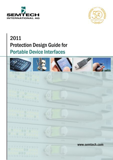
2011<br />
Protection Design Guide for<br />
Portable Device Interfaces<br />
www.semtech.com
Table of Contents<br />
Portable Device Interfaces Protection<br />
Section I: Introduction & Background<br />
Trends in circuit protection > 4<br />
<strong>Semtech</strong> advantages process & technology > 5<br />
Threat environment > 6<br />
TVS diode basics > 8<br />
Clamping voltage > 9<br />
Layout guidelines > 10<br />
Section II: Protection Solutions<br />
Parts & features > 11<br />
Antenna protection (RClamp ® 0531T) > 14<br />
High speed interfaces protection (RClamp ® 0544T) > 15<br />
USB protection (RClamp ® 0542T) > 16<br />
USB with integration VBus protection (RClamp ® 1624T, RClamp ® 3624T) > 17<br />
SD/MicroSD protection (EClamp ® 2410P) > 18<br />
Audio port protection (EClamp ® 2422N ) > 19<br />
SIM card protection (EClamp ® 2465T) > 20<br />
LCD display and camera protection (EClamp ® 250xK) > 21<br />
Keypads and sidekeys protection (µClamp ® 0501T, µClamp ® 0511T) > 22<br />
Low voltage keypads and sidekeys (µClamp ® 2511T, µClamp ® 3311T) > 23<br />
Section III: Protection Applications<br />
IEC61000-4-x Transient Immunity Standards > 25<br />
HDMI protection > 29<br />
LVDS protection > 30<br />
USB protection > 31<br />
EPD low voltage TVS > 32<br />
TVS diode selection > 33<br />
Unidirectional vs. bidirectional protection > 34<br />
TVS package drawings > 35
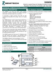
Introduction & Background<br />
Portable Device Interfaces Protection<br />
The Need for Robust Circuit Protection<br />
Today’s mobile communication integrated circuits (ICs) are faster, more<br />
efficient, consume less power, and are smaller than ever before. Yet the<br />
advances in IC technology and enhanced chip performance has come with<br />
a notable trade off: increased susceptibility to damage from ESD, cable<br />
discharge and lightning. Not only are transistor geometry sizes scaling down<br />
at a remarkable pace, leading to more sensitive circuits, but the on-chip<br />
protection is increasingly being sacrificed in favor of accommodating greater<br />
performance in the chip. As this trend progresses, high performance system<br />
level transient voltage protection will be needed more than ever before.<br />
Cost of ESD design dependent on:<br />
• Chip area<br />
• Respins<br />
• Resources<br />
• Circuit performance<br />
• Time-to-market<br />
2kV HBM Level<br />
1kV HBM Level<br />
Safe Handling Level<br />
ESD Association’s Recommended<br />
Safe-Handling Level for On-Chip Protection<br />
Protection Design Guide ©2011 Copyright <strong>Semtech</strong> Corporation. All rights reserved. All Clamp products are registered trademarks of <strong>Semtech</strong> Corporation. 4
Introduction & Background<br />
Portable Device Interfaces Protection<br />
<strong>Semtech</strong> Advantages<br />
Process & Technology<br />
The <strong>Semtech</strong> protection portfolio offers key advantages over industry standard TVS<br />
protection devices. These performance advantages are achieved with <strong>Semtech</strong>’s<br />
advanced processing technology. This process technology enables the production<br />
of TVS diode arrays with sub 5 volt working voltage, low clamping voltage, and<br />
sub-picofarad capacitance. The compact design of the <strong>Semtech</strong> process allows<br />
devices to be housed in low-profile, space-saving packages. Lower working voltage<br />
means that the protection device can respond more quickly, shunt transient voltage<br />
spikes at a lower threshold, and thus provide a lower clamping voltage. As the<br />
transient voltage sensitivity of transceivers increases, designing low working voltage<br />
protection devices is a critical component for protecting today’s systems.<br />
Protection Design Guide ©2011 Copyright <strong>Semtech</strong> Corporation. All rights reserved. All Clamp products are registered trademarks of <strong>Semtech</strong> Corporation. 5
Introduction & Background<br />
Portable Device Interfaces Protection<br />
Threat Environment<br />
Portable electronics interfaces are vulnerable to a variety of different transient voltage threats. These threats include Electrostatic<br />
Discharge (ESD) and Cable Discharge Events (CDE). Interfaces that are accessible to human contact, such as USB ports, are vulnerable to<br />
transient voltage threats from ESD and cable discharge transients. When choosing and designing an appropriate protection scheme, you<br />
should consider these transients and their inherent electrical characteristics.<br />
Electrostatic Discharge (ESD)<br />
Several models exist to simulate ESD events. Each is designed<br />
to describe the threat in a real world environment. The discharge<br />
model is typically a voltage source feeding a resistor/capacitor<br />
network. Resistor and capacitor values vary depending upon the<br />
standard. Today the most internationally recognized ESD standard<br />
is IEC 61000-4-2. IEC 61000-4-2 is a system level standard used<br />
by manufacturers to model ESD events from human contact. The<br />
test is performed by discharging a 150pF capacitor through a<br />
330Ω resistor. Discharge into the equipment may be through direct<br />
contact (contact discharge) or just prior to contact (air discharge).<br />
IEC 61000-4-2 divides the ESD into four threat levels. Test voltages<br />
at the threat levels range from 2kV to 15kV with peak discharge<br />
currents as high as 30A. Most manufacturers adhere to the most<br />
stringent level, level 4, which defines a +/-15kV air discharge test<br />
and a +/-8kV contact discharge test. However, many manufacturers<br />
test their equipment beyond these levels. The ESD waveform as<br />
defined by IEC 61000-4-2 reaches peak magnitude in 700ps to 1ns<br />
and has a total duration of only 60ns. While the ESD pulse contains<br />
little energy, the resulting effect can be devastating to sensitive<br />
semiconductor devices. Sensitive points of the equipment are to be<br />
tested with a combination of positive and negative discharges.<br />
I peak I<br />
100%<br />
90%<br />
I at 30 ns<br />
I at 60 ns<br />
10%<br />
Level<br />
ESD Discharge Levels per IEC61000-4-2<br />
Test Voltage<br />
Air Discharge<br />
(kV)<br />
Test Voltage<br />
Contact<br />
Discharge<br />
(kV)<br />
First<br />
Peak<br />
Current<br />
(A)<br />
Peak<br />
Current<br />
at 30 ns<br />
(A)<br />
Peak<br />
Current<br />
at 60 ns<br />
(A)<br />
1 2 2 7.5 4 2<br />
2 4 4 15 8 4<br />
3 8 6 22.5 12 6<br />
4 15 8 30 16 8<br />
30 ns<br />
60 ns<br />
t<br />
tr = 0.7 to 1 ns<br />
ESD Waveform per IEC 61000-4-2<br />
Protection Design Guide ©2011 Copyright <strong>Semtech</strong> Corporation. All rights reserved. All Clamp products are registered trademarks of <strong>Semtech</strong> Corporation. 6
Introduction & Background<br />
Portable Device Interfaces Protection<br />
ESD Immunity: System Level vs. Device Level<br />
For ESD immunity, it is important to distinguish between system<br />
level immunity and device level immunity. The JEDEC JESD22-<br />
A114E which is equivalent to the earlier Mil-Std-883 is a device<br />
level standard appropriate for the level of ESD threat seen in<br />
the manufacturing environment. The IEC 61000-4-2 standard is<br />
intended to describe the level of ESD threat seen in the system<br />
environment. In the case of transceiver ICs, most are rated to 2kV<br />
Human Body Model (HBM) according to the JEDEC Standard/Mil-<br />
Std 883. This is not the same as 2kV for the system level standard<br />
(IEC 61000-4-2). In fact, the IEC pulse, for a given voltage level, will<br />
render over 5 times higher current levels than the JEDEC standard.<br />
The chart illustrates this difference: a 2kV ESD pulse for the JEDEC<br />
Standard renders a peak current of approximately 1.33A. For the<br />
system level, that same 2kV charge level corresponds to a peak<br />
current of 7.5A.<br />
IEC Level<br />
(Contact<br />
discharge)<br />
Peak Current IEC vs JEDEC<br />
ESD<br />
Voltage<br />
(kV)<br />
JEDEC JESD-<br />
A114E Ipp (kV)<br />
IEC 61000-4-2<br />
Ipp (A)<br />
1 2 1.33 7.5<br />
2 4 2.67 15<br />
3 6 4.00 22.5<br />
4 8 5.33 30<br />
ESD Immunity Standards: IEC61000-4-2 vs. JESD22-A114E<br />
To achieve high system level ESD immunity, you should adhere<br />
to the IEC 61000-4-2 standard. The IEC standard is more closely<br />
representative of the real world ESD threats seen by electronic<br />
systems. Most commercial designs require passing minimum of<br />
±8kV for the Human Body Model of IEC (level 4) contact discharge.<br />
Protection Design Guide ©2011 Copyright <strong>Semtech</strong> Corporation. All rights reserved. All Clamp products are registered trademarks of <strong>Semtech</strong> Corporation. 7
Introduction & Background<br />
Portable Device Interfaces Protection<br />
TVS Diode Basics<br />
Transient Voltage Suppression (TVS) Diodes<br />
Transient Voltage Suppressor (TVS) diodes have long been used<br />
to provide robust circuit protection. As shown in the following<br />
diagram, TVS diodes are generally connected as shunt elements<br />
across a transmission line. Under normal operating conditions<br />
the TVS diode presents a high impedance to the protected circuit.<br />
During a transient event, the TVS achieves breakdown, presents<br />
a low impedance shunt path, and the transient current is shunted<br />
through the TVS diode. A good TVS protection circuit must divert<br />
transient current and clamp transient voltage below the failure<br />
threshold of the protected IC.<br />
Voltage<br />
ESD Event<br />
Transient<br />
Enviroment<br />
Z in<br />
TVS<br />
Diode<br />
TVS Diode Operation<br />
Protected<br />
Circuit<br />
Parameters for Effective Circuit Protection<br />
A good TVS device for protecting dataline communications<br />
interfaces must have some key parameters. First, low working<br />
voltage is a critical TVS parameter for safeguarding submicron<br />
integrated circuits. The working voltage, or Vrwm, is the maximum<br />
rated DC voltage for the TVS device. At the Vrwm voltage, the TVS<br />
is still a non-conducting device. Once the transient voltage rises<br />
above the working voltage, the TVS quickly achieves breakdown<br />
and presents a low impedance path to divert the transient. Thus,<br />
a low working voltage is essential for clamping a transient to<br />
a level well below the damage threshold of the IC that the TVS<br />
is protecting. The I-V curve illustrates the advantage of a lower<br />
working voltage. The green line represents a typical I-V curve for a<br />
standard TVS device while the red I-V curve illustrates the <strong>Semtech</strong>’s<br />
low working voltage technology. The lower working voltage means the<br />
transient voltage is arrested more quickly and thus can be clamped<br />
to a lower voltage. Using TVS devices with lower working voltage<br />
is critical to reducing the stress energy seen by the application<br />
processor. To address this need, <strong>Semtech</strong> has designed a family<br />
of 2.5V working voltage protection devices for safeguarding next<br />
generation application processors and baseband ICs.<br />
Secondly, the TVS should present low capacitance to preserve<br />
signal integrity on the high-speed interface. If the capacitance of<br />
the TVS diodes is too high, adding excessive loading to the circuit,<br />
signal distortion and data errors will result.<br />
I (Amps)<br />
2.5 V<br />
Vrwm<br />
Vclamp<br />
V (Volts)<br />
Typical 5V TVS IV Curve<br />
<strong>Semtech</strong> Low Vrwm IV Curve<br />
IV Curve for <strong>Semtech</strong> Low Working Voltage Process<br />
Protection Design Guide ©2011 Copyright <strong>Semtech</strong> Corporation. All rights reserved. All Clamp products are registered trademarks of <strong>Semtech</strong> Corporation. 8
Introduction & Background<br />
Portable Device Interfaces Protection<br />
Clamping Voltage<br />
Clamping voltage, by definition, is the maximum voltage drop<br />
across the protection device during a transient event, which is also<br />
the stress voltage seen by the protected IC. The clamping voltage is<br />
the most critical parameter to consider when choosing a TVS device.<br />
It is important to note that a device rated at IEC 61000-4-2 does<br />
not guarantee the system will pass ESD testing. This is because<br />
the IEC is a system level standard that was originally intended to be<br />
applied as pass/fail criteria for showing system level ESD immunity.<br />
The purpose of a protection device is to reduce a transient voltage<br />
spike down to a safe voltage for the protected IC, and the best way<br />
to insure that your TVS protection device adequately protects your<br />
interface circuitry is by choosing components that offer the lowest<br />
clamping voltage performance.<br />
To illustrate the unique protection benefits of <strong>Semtech</strong>’s proprietary<br />
EPD technology, the following chart compares the clamping voltage<br />
of an industry standard 5V TVS device with the clamping voltage of<br />
the <strong>Semtech</strong> 2.5V TVS device. Built on the EPD platform, this device<br />
offers a very low 2.5V working voltage. Notice that the <strong>Semtech</strong> 2.5V<br />
TVS provides a nice low, flat clamping voltage over a wide range<br />
of peak pulse current values. As a 2.5V working voltage device,<br />
the clamping performance of the 2.5V TVS is significantly lower<br />
than the typical 5V TVS protection device. As the sensitivity on next<br />
generation ICs increases, selecting TVS devices with a lower clamping<br />
voltage as illustrated in the chart can impact the difference<br />
between safeguarding an IC or resulting in catastrophic damage.<br />
Clamping Voltage vs Peak Pulse Current<br />
Clamping Voltage - V C (V)<br />
12<br />
10<br />
8<br />
6<br />
4<br />
2<br />
0<br />
Typical 5V<br />
ESD Protection<br />
0 2 4 6 8 10 12<br />
Peak Pulse Current - I PP (A)<br />
Clamping Performance for <strong>Semtech</strong> 2.5V TVS<br />
<strong>Semtech</strong> 2.5V TVS<br />
Waveform<br />
Parameters:<br />
tr = 8µs<br />
td = 20µs<br />
Protection Design Guide ©2011 Copyright <strong>Semtech</strong> Corporation. All rights reserved. All Clamp products are registered trademarks of <strong>Semtech</strong> Corporation. 9
Introduction & Background<br />
Portable Device Interfaces Protection<br />
Layout Guidelines<br />
PC board layout is an important part of transient immunity design.<br />
This is especially critical in portable device applications, where<br />
protecting the constant threat of ESD and CDE from normal use is<br />
further complicated by the high speed of the link rates. Parasitic<br />
inductance in the protection path can result in significant voltage<br />
overshoot and may exceed the damage threshold of the protected<br />
IC. This is especially critical in the case of fast rise-time transients<br />
such as ESD or EFT. Recall that the voltage developed across an<br />
inductive load is proportional to the time rate of change in current (V<br />
= L di/dt). An ESD induced transient reaches a peak in less than<br />
1ns (per IEC 61000-4-2). Assuming a trace inductance of 20nH per<br />
inch and a quarter inch trace, the voltage overshoot will be 50 volts<br />
for a 10A pulse.<br />
The primary rule of thumb is to minimize the effects of parasitic<br />
inductance by making the shunt paths as short as possible. All<br />
inductive paths must be considered including the ground return<br />
path, the path between the TVS and the protected line, and the<br />
path from the connector to the TVS device. Additionally, The TVS<br />
device should be placed as close to the entry point of ESD as<br />
possible to reduce transient coupling into nearby traces.<br />
The secondary effects of radiated emissions can cause upset<br />
to other areas of the board even if there is no direct path to the<br />
connector. Long signal traces will act as antennas to receive energy<br />
from fields that are produced by the ESD pulse. By keeping line<br />
lengths as short as possible, the efficiency of the line to act as an<br />
antenna for ESD related fields is reduced. Minimize interconnecting<br />
line lengths by placing devices with the most interconnects as close<br />
together as possible. Finally, avoid running critical signal lines near<br />
board edges or next to protected lines.<br />
Vcc<br />
Vcc<br />
L1<br />
Vp1 = L1 * di/dt<br />
Protected<br />
IC<br />
Vc = Clamping Voltage of TVS<br />
Vtotal = Vc + Vp1 + Vp2<br />
GND<br />
L2<br />
Vp2 = L2 * di/dt<br />
* L1 represents the parasitic inductance of the trace between TVS and Vcc<br />
* L2 represents the parasitic inductance of the trace between TVS and GND<br />
* Vtotal represents the voltage that will be see between Vcc and GND of the IC during a transient.<br />
Protection Design Guide ©2011 Copyright <strong>Semtech</strong> Corporation. All rights reserved. All Clamp products are registered trademarks of <strong>Semtech</strong> Corporation. 10
Parts & Features<br />
Portable Device Interfaces Protection<br />
Parts & Features<br />
ESD sensitive interfaces are found through out today’s advanced portable devices<br />
increasing the need for high performance protection solutions. <strong>Semtech</strong>’s industry<br />
leading low-clamping voltage, low capacitance, and innovative packaging provide<br />
advanced performance solutions to safeguard your systems from transient voltage<br />
threats. This section will highlight some of the newly released key portable product<br />
devices within the <strong>Semtech</strong> protection portfolio.<br />
Protection Design Guide ©2011 Copyright <strong>Semtech</strong> Corporation. All rights reserved. All Clamp products are registered trademarks of <strong>Semtech</strong> Corporation. 11
Parts & Features<br />
Portable Device Interfaces Protection<br />
Part Number Lines V rwm<br />
Cap I/O<br />
to I/O<br />
Ipp max<br />
(8x20μs)<br />
Application<br />
Circuit Diagram<br />
RClamp ® 0531T 1 5V 0.5pF 4A Antenna<br />
1.0 x 0.6 x 0.4 mm<br />
RClamp ® 0544T 4 5V 0.3pF 5A<br />
HDMI<br />
MicroSD<br />
LVDS<br />
2.0 x 1.0 x 0.4 mm<br />
RClamp0544T<br />
RClamp ® 0542T 2 5V<br />
0.4pF<br />
max<br />
5A<br />
HDMI<br />
LVDS<br />
USB2.0 & 3.0<br />
1.6 x 1.0 x 0.4 mm<br />
RClamp0522T<br />
VBus<br />
1<br />
GND<br />
RClamp ® 1624T<br />
3<br />
1<br />
5.5V<br />
12V<br />
0.4pF max<br />
5A<br />
5A<br />
USB<br />
VBUS<br />
DM<br />
DP<br />
ID<br />
GND<br />
1.7 x 1.0 x 0.4 mm<br />
VBus<br />
1<br />
GND<br />
RClamp ® 3624T<br />
3<br />
1<br />
5.5V<br />
28V<br />
0.4pF max<br />
6A<br />
8A<br />
USB<br />
VBUS<br />
DM<br />
DP<br />
ID<br />
GND<br />
1.7 x 1.0 x 0.4 mm<br />
EClamp ® 2410P 6 5V - - MicroSD<br />
4.0 x 1.6 x 0.58 mm<br />
GND<br />
EClamp ® 2422N 2 5V 100pF - Audio<br />
GND<br />
1.45 x 1.0 x 0.58 mm<br />
Protection Design Guide ©2011 Copyright <strong>Semtech</strong> Corporation. All rights reserved. All Clamp products are registered trademarks of <strong>Semtech</strong> Corporation. 12
Parts & Features<br />
Portable Device Interfaces Protection<br />
Part Number Lines V rwm<br />
Cap I/O<br />
to I/O<br />
Ipp max<br />
(8x20μs)<br />
Application<br />
Circuit Diagram<br />
EClamp ® 2465T 4 5V 10pF - SIM Cards<br />
1.7 x 1.3 x 0.4 mm<br />
EClamp ® 2504K 4 5V 15pF typ -<br />
LCD Display<br />
Camera<br />
1.7 x 1.3 x 0.5 mm<br />
EClamp ® 2506K 6 5V 15pF -<br />
LCD Display<br />
Camera<br />
2.5 x 1.3 x 0.5 mm<br />
EClamp ® 2508K 8 5V 15pF -<br />
LCD Display<br />
Camera<br />
3.3 x 1.3 x 0.5 mm<br />
µClamp ® 0501T 1 5V 10pF max 2A<br />
Keypads<br />
Sidekeys<br />
Connectors<br />
1.0 x 0.6 x 0.4 mm<br />
µClamp ® 0511T 1 5V 7pF max 2A<br />
Keypads<br />
Sidekeys<br />
Connectors<br />
1.0 x 0.6 x 0.4 mm<br />
µClamp ® 2511T 1 2.5V 7pF max 5A<br />
Keypads<br />
Sidekeys<br />
Audio<br />
Antenna<br />
1.0 x 0.6 x 0.4 mm<br />
µClamp ® 3311T 1 3.3V 10pF max 5A<br />
Keypads<br />
Sidekeys<br />
Audio<br />
Antenna<br />
1.0 x 0.6 x 0.4 mm<br />
Protection Design Guide ©2011 Copyright <strong>Semtech</strong> Corporation. All rights reserved. All Clamp products are registered trademarks of <strong>Semtech</strong> Corporation. 13
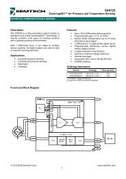
Protection Solutions<br />
Portable Device Interfaces Protection<br />
RClamp ® 0531T<br />
ESD Protection for Low Frequency Antenna<br />
Features<br />
• 5V working voltage<br />
• 1-line bidirectional<br />
• Capacitance: typical 0.5pF<br />
• Low clamping voltage<br />
• No insertion loss up to 2.5GHz<br />
• Ultra small package (1.0 x 0.6 x 0.4 mm)<br />
Applications<br />
• GPS antennas<br />
• FM antennas<br />
• LVDS<br />
• High speed data lines<br />
Description<br />
The RClamp0531T is a bidirectional single line protection<br />
device offering a maximum capacitance of 0.80pF. This allows<br />
it to be used on circuits operating in excess of 2.5GHz without<br />
signal attenuation. They may be used to meet the ESD immunity<br />
requirements of IEC 61000-4-2, Level 4.<br />
This device is packaged in a 2-pin, RoHS/WEEE compliance,<br />
SLP1006P2T package measuring 1.0 x 0.6 x 0.4 mm. Each device<br />
protects one high-speed line operating at 5 volts. It gives the<br />
designer the flexibility to protect single lines in applications where<br />
arrays are not practical.<br />
RClamp0531T<br />
Ultra low capacitance RClamp0531T featuring<br />
superior clamping performance protecting<br />
today’s sensitive IC’s.<br />
ESD Sensitive<br />
Circuit<br />
High speed single line ESD protection<br />
Protection Design Guide ©2011 Copyright <strong>Semtech</strong> Corporation. All rights reserved. All Clamp products are registered trademarks of <strong>Semtech</strong> Corporation. 14
Protection Solutions<br />
Portable Device Interfaces Protection<br />
RClamp ® 0544T<br />
ESD Protection for HDMI and other High Speed Interfaces<br />
Features<br />
• 5V working voltage<br />
• 4-line protection<br />
• Capacitance: typical 0.3pF Line-to-Line<br />
• Low-clamping voltage<br />
• No impedance matching required<br />
• No Insertion loss up to 3.0GHz<br />
• Ultra-small leadless package (2.0 x 1.0 x 0.4 mm)<br />
Applications<br />
• Mini HDMI<br />
• HDMI 1.3 / 1.4<br />
• LVDS<br />
• DisplayPort<br />
• USB 2.0<br />
Description<br />
The RClamp0544T is a 4-line protection device operating at 5V.<br />
It has a typical capacitance of only 0.30pF between I/O pins.<br />
This allows it to be used on circuits operating in excess of 3GHz<br />
without signal attenuation. They may be used to ESD immunity<br />
requirements of IEC 61000-4-2, Level 4 (±15kV air, ±8kV contact<br />
discharge).<br />
The RClamp0544T is in a 8-pin, RoHS/WEEE compliant,<br />
SLP2010P8T package. It measures 2.0 x 1.0 x 0.4 mm. The leads<br />
are spaced at a pitch of 0.4mm and are designed for easy PCB<br />
layout by allowing the traces to run straight through the device.<br />
RClamp0544T<br />
RClamp0544T<br />
Data 2+<br />
Data 2-<br />
High performance, ultra low<br />
capacitance ESD protection for<br />
maximum signal integrity in a<br />
flow through package.<br />
Data 1+<br />
Data 1-<br />
Data 0+<br />
To HDMI<br />
Graphics Chip<br />
HDMI<br />
Connector<br />
Data 0-<br />
CLK +<br />
CLK -<br />
RClamp0544T (3 Each)<br />
CEC<br />
SCL<br />
SDA<br />
HP Detect<br />
5V Power<br />
GND<br />
Protection for HDMI Interface<br />
Protection Design Guide ©2011 Copyright <strong>Semtech</strong> Corporation. All rights reserved. All Clamp products are registered trademarks of <strong>Semtech</strong> Corporation. 15
Protection Solutions<br />
Portable Device Interfaces Protection<br />
RClamp ® 0542T<br />
ESD Protection for USB 2.0 / 3.0 and other<br />
High Speed Interfaces<br />
Features<br />
• 5V Working Voltage<br />
• 2-line protection<br />
• Capacitance: typical 0.3pF Line-to-Line<br />
• Low-clamping voltage<br />
• No insertion loss up to 3.0GHz<br />
• Small leadless package: 1.6 x 1.0 x 0.4 mm<br />
Applications<br />
• USB 2.0 / 3.0<br />
• HDMI 1.3 / 1.4<br />
• LVDS<br />
• DisplayPort<br />
Description<br />
The RClamp0542T has typical capacitance of only 0.3pF (line-toline).<br />
This means it can be used on circuits operating in excess of<br />
3GHz without signal attenuation. They may be used to meet the<br />
ESD immunity requirements of IEC 61000-4-2, Level 4 (±15kV air,<br />
±8kV contact discharge). Each device can be configured to protect<br />
1 bidirectional line or two unidirectional lines.<br />
These devices are in a small leadless package (SLP1610P4T)<br />
package and feature a lead-free, matte tin finish. They are compatible<br />
with both lead free and SnPb assembly techniques. They are designed<br />
for use in applications where board space is at a premium.<br />
RClamp0542T<br />
RClamp0542T flow through design allows for<br />
a designers flexibility for part placement.<br />
RClamp0542T<br />
USB Connector<br />
USB Controller<br />
Vbus<br />
D-<br />
D-<br />
D+<br />
D+<br />
RClamp0542T<br />
Gnd<br />
RClamp0542T USB 2.0 Protection<br />
Protection Design Guide ©2011 Copyright <strong>Semtech</strong> Corporation. All rights reserved. All Clamp products are registered trademarks of <strong>Semtech</strong> Corporation. 16
Protection Solutions<br />
Portable Device Interfaces Protection<br />
RClamp ® 1624T/RClamp ® 3624T<br />
ESD Protection for USB 2.0 with<br />
Integrated 5V VBus Protection<br />
Features<br />
• Protects three I/O lines operating up to 5.5V<br />
• RClamp1624T protects Vbus line operating up to 12V<br />
• RClamp3624T protects Vbus line operating up to 28V<br />
• Capacitance: typical 0.8pF Line-to-ground<br />
• Low clamping voltage<br />
• No insertion loss up to 2.0GHz<br />
• Large ground for increased ESD performance<br />
• Small package (1.7 x 1.0 x 0.4 mm)<br />
Applications<br />
• USB 2.0<br />
• USB OTG<br />
Description<br />
The RClamp1624T and Rclamp3624T are specifically designed<br />
to protect one USB port. The flow through layout design of the<br />
package enables designers greater flexibility with maximum signal<br />
integrity. The unique design of this device features low capacitance<br />
TVS diodes for protection of the USB data (DP, DM) and USB ID pins<br />
operating at 5V. Loading capacitance on these lines is
Protection Solutions<br />
Portable Device Interfaces Protection<br />
EClamp ® 2410P<br />
ESD/EMI Protection for Multimedia Cards<br />
Features<br />
• 5V working voltage<br />
• Protection & termination for six lines & Vdd<br />
• Capacitance: typical 12pF per line<br />
• Termination resistors: 45Ω<br />
• Pull up resistors: 15kΩ (2 each) and 50kΩ<br />
• 16 Pin leadless package (4.0 x 1.6 x 0.58 mm)<br />
Applications<br />
• T-Flash / MicroSD interfaces<br />
• MMC interfaces<br />
Description<br />
The EClamp2410P is a combination EMI filter and line termination<br />
device with integrated TVS diodes for use on Multimedia Card<br />
Interfaces. They have been optimized for protection of T-Flash/<br />
MicroSD interfaces in cellular phones and other portable devices.<br />
The device consists of six circuits that include series impedance<br />
matching resistors and pull up resistors as required by the SD<br />
specification. TVS diodes are included on each line for ESD protection.<br />
An additional TVS diode connection is included for protection of the<br />
voltage (Vdd) bus. Termination resistor value of 45Ω is included on<br />
the DAT0, DAT1, DAT2, DAT3, CMD, and CLK lines. Pull up resistors<br />
of 15kΩ are included on DAT0, DAT1, DAT 2, and CMD lines while<br />
a 50kΩ pull up resistors included on the DAT3 line. These may be<br />
configured for devices operating in SD or SPI mode.<br />
EClamp2410P<br />
MicroSD protection with integrated EMI/TVS<br />
protection saving valuable PCB board space.<br />
Vss<br />
DAT 1 IN<br />
DAT 0 IN<br />
CLK IN<br />
Rup 15Ku<br />
VDD<br />
CMD IN<br />
DAT 3 IN<br />
DAT 2 IN<br />
1 16<br />
DAT 1 OUT<br />
DAT 0 OUT<br />
CLK OUT<br />
Rup 15Ku<br />
Rup 50Ku<br />
CMD OUT<br />
DAT 3 OUT<br />
DAT 2 OUT<br />
HOST IC<br />
Protection for MicroSD Interface<br />
Protection Design Guide ©2011 Copyright <strong>Semtech</strong> Corporation. All rights reserved. All Clamp products are registered trademarks of <strong>Semtech</strong> Corporation. 18
Protection Solutions<br />
Portable Device Interfaces Protection<br />
EClamp ® 2422N<br />
ESD/EMI Protection for Audio Interfaces<br />
Features<br />
• 5V working voltage<br />
• Protection and filtering for two lines<br />
• Capacitors: 100pF (Typical VR=0v)<br />
• Inductor: 2nH (Typical)<br />
• Small leadless package (1.45 x 1.0 x 0.58 mm)<br />
Description<br />
The EClamp2422N is a (C-L-C) low pass filter array with integrated<br />
TVS diodes. It is designed to suppress unwanted EMI/RFI signals<br />
and provide ESD protection for audio interfaces. Two identical<br />
circuits consisting of an inductor of 2nH and capacitor value of<br />
100pF, which are used to achieve 10dB minimum attenuation from<br />
800MHz to 2.7GHz. It has a very low series resistance of 2.OΩ,<br />
making it ideal for use on speaker/microphone interfaces.<br />
Applications<br />
• Speaker ports<br />
• Microphone ports<br />
EClamp2422N<br />
Flow through design allows for efficient PCB layout.<br />
Integrated low pass filter reduces part count.<br />
V2<br />
V1<br />
Vin +<br />
Vin −<br />
Differential Mode Protection with Speaker Output<br />
Protection of Single-Ended Mode Microphone<br />
with Speaker Output<br />
Protection Design Guide ©2011 Copyright <strong>Semtech</strong> Corporation. All rights reserved. All Clamp products are registered trademarks of <strong>Semtech</strong> Corporation. 19
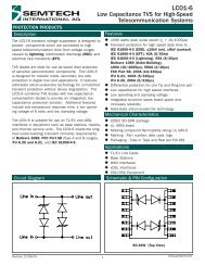
Protection Solutions<br />
Portable Device Interfaces Protection<br />
EClamp ® 2465T<br />
ESD/EMI Protection for SIM Card in Portable Products<br />
Features<br />
• 5V working voltage<br />
• 4-line protection and filtering<br />
• Capacitance: 10pF<br />
• Termination resistors: 100Ω & 47Ω<br />
• Low ESD clamping voltage<br />
• Very small package (1.7 x 1.3 x 0.4 mm)<br />
Applications<br />
• Smartphones<br />
• Portable electronics<br />
• MIDs<br />
• Tablet computers<br />
Description<br />
The EClamp2465T is a combination EMI filter and line termination<br />
device with integrated TVS diodes for use on SIM card interfaces on<br />
cellular phones and other portable electronics. The device consists<br />
of three circuits that include series impedance matching resistors<br />
for proper termination of the SIM card interface. Termination<br />
resistor value of 100Ω is included on the Reset and Data lines and<br />
47Ω on the CLK line. TVS diodes are also included on each line<br />
for ESD protection in excess of ±15kV (air discharge) and ±8kV<br />
(contact discharge) per IEC61000-4-2, level 4. An additional TVS<br />
diode connection is included for protection of the voltage (Vcc) bus.<br />
Pin Description<br />
1 Data to Connector<br />
2 CLK to Connector<br />
3 Reset to Connector<br />
4 N/C<br />
5 Data to IC<br />
6 CLK to IC<br />
7 Reset to IC<br />
8 Vcc to Connector<br />
Ultra-small, 4-line EClamp2465T provides<br />
superior ESD/EMI protection for today’s<br />
advanced portable products<br />
1 8<br />
1<br />
2<br />
3<br />
4<br />
5<br />
6<br />
To IC<br />
4<br />
5<br />
Protection for SIM Card Interface<br />
Protection Design Guide ©2011 Copyright <strong>Semtech</strong> Corporation. All rights reserved. All Clamp products are registered trademarks of <strong>Semtech</strong> Corporation. 20
Protection Solutions<br />
Portable Device Interfaces Protection<br />
EClamp ® 250xK<br />
Advanced EMI Filtering and ESD protection for<br />
portable applications<br />
Features<br />
• 5V working voltage<br />
• Three pole LC filter<br />
• Inductor: 17nH (Typical)<br />
• Total capacitance: 24pF (Typical)<br />
• Available in 4, 6, and 8 line protection<br />
• 20dB minimum attenuation between 800MHz to 2.7GHz<br />
• Meets IEC61000-4-2 level 4<br />
Description<br />
The EClamp250xK family are low pass filter array’s with integrated<br />
TVS diodes. They are designed to suppress unwanted EMI/RFI<br />
signals and provide ESD protection in portable electronics. These<br />
devices consist of four, six, or eight identical circuits comprised<br />
of TVS diodes for ESD protection and a 3-pole inductor-capacitor<br />
network for EMI/RFI filtering. A typical inductor value of 17nH and<br />
a capacitor value of 12pF are used to achieve 20dB minimum<br />
attenuation from 800MHz to 2.7GHz. The TVS diodes provide<br />
effective suppression of ESD voltages in excess of ±15kV (air<br />
discharge) and ±8kV (contact discharge) per IEC 61000-4-2, level 4.<br />
Applications<br />
• Color LCD protection<br />
• Cell phone CCD camera lines<br />
Three Pole LC EMI/ESD<br />
protection for today’s<br />
advanced LCD displays.<br />
EClamp2504K EClamp2506K EClamp2508K<br />
Display<br />
Controller<br />
Protection Design Guide ©2011 Copyright <strong>Semtech</strong> Corporation. All rights reserved. All Clamp products are registered trademarks of <strong>Semtech</strong> Corporation. 21
Protection Solutions<br />
Portable Device Interfaces Protection<br />
µClamp ® 0501T & µClamp ® 0511T<br />
ESD Protection for keypads and sidekeys<br />
Features<br />
• 5V working voltage<br />
• Single line protection<br />
• µClamp0501T Unidirectional protection<br />
• µClamp0501T Capacitance: 10pF (max)<br />
• µClamp0511T Bidirectional protection<br />
• µClamp0511T Capacitance: 7pF (max)<br />
• Excellent ESD Clamping<br />
Description<br />
These µClamp devices are designed to protect sensitive electronics<br />
from damage or latch-up due to ESD. It is designed to replace<br />
multilayer varistors (MLVs) in portable applications such as cell<br />
phones, notebook computers, and other portable electronics. It<br />
features large cross-sectional area junctions for conducting high<br />
transient currents. They offer desirable characteristics for board<br />
level protection including fast response time, low operating and<br />
clamping voltage and no device degradation. It may be used to<br />
meet the ESD immunity requirements of IEC 61000-4-2, Level 4<br />
(±15kV air, ±8kV contact discharge).<br />
Applications<br />
• Keypad protection<br />
• Sidekey protecion<br />
• Portable electronics<br />
• Multimedia card interfaces<br />
µClamp0501T<br />
µClamp0511T<br />
The µClamp0501T and µClamp0511T feature<br />
advanced designs allowing for low capacitance<br />
along with industry leading ESD clamping<br />
Keypad<br />
*<br />
7<br />
4<br />
1<br />
R1<br />
0<br />
8<br />
5<br />
2<br />
R2<br />
#<br />
9<br />
6<br />
3<br />
R3<br />
C1<br />
C2<br />
C3<br />
C4<br />
Keypad array protection with µClamp0511T<br />
Protection Design Guide ©2011 Copyright <strong>Semtech</strong> Corporation. All rights reserved. All Clamp products are registered trademarks of <strong>Semtech</strong> Corporation. 22
Protection Solutions<br />
Portable Device Interfaces Protection<br />
µClamp ® 2511T & µClamp ® 3311T<br />
ESD protection for low voltage applications<br />
Features<br />
• µClamp2511T - 2.5V working voltage<br />
• µClamp3311T - 3.3V working voltage<br />
• Single line protection<br />
• Low clamping voltage<br />
• Low leakage current: 10nA (typ)<br />
• Low capacitance: 10pF (max)<br />
• Bidirectional protection<br />
Applications<br />
• Keypads and sidekeys<br />
• GPS, TV, and FM antennas<br />
• Audio<br />
Description<br />
The low voltage uClamp series of TVS devices are designed to<br />
replace multilayer varistors (MLVs) in portable applications such as<br />
cell phones and notebook computers. They are designed to protect<br />
sensitive semiconductor components from damage or upset due<br />
to electrostatic discharge events. Both devices are constructed<br />
using <strong>Semtech</strong>’s proprietary EPD process technology. The EPD<br />
process provides a low standoff voltage with a significant reduction<br />
in leakage current and capacitance. They feature true operating<br />
voltages of 2.5V and 3.3V for superior protection when compared<br />
to traditional pn junction devices.<br />
µClamp2511T and µClamp3311T<br />
True low voltage protection featuring an<br />
industry leading clamping ESD performance<br />
for 2.5V and 3.3V applications.<br />
I (Amps)<br />
2.5V<br />
5V<br />
V (Volts)<br />
Low Voltage IV Curve vs. Traditional 5V TVS<br />
Protection Design Guide ©2011 Copyright <strong>Semtech</strong> Corporation. All rights reserved. All Clamp products are registered trademarks of <strong>Semtech</strong> Corporation. 23
Applications<br />
Portable Device Interfaces Protection<br />
Circuit Protection Applications<br />
As high speed interfaces can be subject to wide variety of transient conditions<br />
and operating environments, the need for good circuit protection solutions<br />
are often unique to the application. This section will examine in deeper<br />
detail some of the more subtle aspects of protecting circuit interfaces from<br />
overvoltage threats.<br />
Protection Design Guide ©2011 Copyright <strong>Semtech</strong> Corporation. All rights reserved. All Clamp products are registered trademarks of <strong>Semtech</strong> Corporation. 24
Applications<br />
Portable Device Interfaces Protection<br />
IEC 61000-4-x Transient Immunity Standards<br />
The International Electrotechnical Commission (IEC), a worldwide<br />
organization promoting international cooperation on questions<br />
concerning standardization in electrical & electronic fields, has<br />
developed transient immunity standards which have become<br />
minimum requirements for manufacturers wanting to do business<br />
in the European Community (EC).<br />
Three of the IEC standards deal with transient immunity:<br />
• IEC 61000-4-2 : Electrostatic Discharge (ESD)<br />
• IEC 61000-4-4 : Electrical Fast Transient/Burst<br />
(Electrical Fast Transients)<br />
• IEC 61000-4-5 : Surge Immunity<br />
The ESD threat is divided into four threat levels. Threat level 1 is<br />
considered the least severe while threat level 4 is the most severe.<br />
Most manufacturers will adhere to level 4: ±8kV contact discharge,<br />
±15kV air discharge. IEC 61000-4-2 also specifies the ESD current<br />
waveform and parameters shown in Figure 1 & Table 1.<br />
I peak<br />
100%<br />
90%<br />
I at 30 ns<br />
I<br />
The following sections provide a summary of each of the transient<br />
immunity standards.<br />
IEC 61000-4-2 – Electrical Discharge (ESD)<br />
Standard<br />
I at 60 ns<br />
10%<br />
30 ns<br />
60 ns<br />
t<br />
IEC 61000-4-2 addresses one of the most common forms of transients<br />
in electronic systems: Electrostatic discharge (ESD). ESD results<br />
from conditions which allow the build up of electrical charge from<br />
contact and separation of two non-conductive materials. When<br />
the charged body is brought in proximity of another object of lower<br />
potential, energy is released in the form of electrostatic discharge.<br />
The standard defines immunity requirements for ESD which can<br />
be coupled into the equipment directly or through radiated effects.<br />
Direct coupling includes any user accessible entry points such<br />
as I/O ports, switches, computer keyboards, panel displays, and<br />
equipment housings. Radiated coupling results from the discharge<br />
between two bodies which are external to the system.<br />
Because the human body is one of the most common generators<br />
of ESD, the IEC standard defines a test set up which is designed<br />
to simulate an ESD event from a human body. The “Human<br />
Body Model” (HBM) as it is referred to, is considered a valid<br />
representation of worst case ESD stresses. Discharge into<br />
equipment may be through direct contact (contact discharge<br />
method) or just prior to contact (air discharge method). Contact<br />
discharge is the preferred test method, but air discharge is used<br />
where contact discharge cannot be applied.<br />
tr = 0.7 to 1 ns<br />
The rise time is extremely fast, defined as 0.7 to 1ns, with a second<br />
peak at 30ns and a total duration of only 60ns. The total energy<br />
contained within the pulse is approximately a few hundred<br />
microjoules.<br />
Transient Voltage Suppression (TVS) diodes are an ideal choice<br />
for meeting the ESD transient immunity requirements of IEC<br />
61000-4-2 and are proven solutions for suppressing system level<br />
ESD events. The extremely fast response time of the TVS diode<br />
is essential for responding to the 1ns rise time of the ESD pulse.<br />
Additionally, TVS diodes are capable of clamping the incoming<br />
transient to a low enough level as not to cause damage to the<br />
protected semiconductor. All TVS diode devices and families<br />
offered by <strong>Semtech</strong> may be used to suppress ESD to level 4 of IEC<br />
61000-4-2. The fast response and low clamping levels make TVS<br />
diodes suitable for ESD suppression on data and I/O ports.<br />
Level<br />
Indicated<br />
Voltage<br />
Figure 1 - ESD Waveform per IEC 61000-42<br />
First peak<br />
current of<br />
discharge<br />
+/- 10%<br />
Rise time<br />
(tr) with<br />
discharge<br />
switch<br />
Current<br />
(+/-<br />
30% at<br />
30 ns)<br />
Current<br />
(+/- 30%<br />
at 60 ns)<br />
kV A ns A A<br />
1 2 7.5 0.7 to 1 4 2<br />
2 4 15 0.7 to 1 8 4<br />
3 6 22.5 0.7 to 1 12 6<br />
4 8 30 0.7 to 1 16 8<br />
Table 1 – IEC61000-4-2 Waveform Parameters<br />
Protection Design Guide ©2011 Copyright <strong>Semtech</strong> Corporation. All rights reserved. All Clamp products are registered trademarks of <strong>Semtech</strong> Corporation. 25
Applications<br />
Portable Device Interfaces Protection<br />
IEC 61000-4-4 – Electrical Fast Transients (EFT)<br />
Immunity Standard<br />
Electrical fast transients occur as a result of arcing contacts in<br />
switches and relays. EFT disturbances are common in industrial<br />
environments where electromechanical switches are used to<br />
connect and disconnect inductive loads. IEC 61000-4-4 specifies<br />
the EFT threat in both power and data lines. The electrical fast<br />
transient is described in terms of a voltage across a 50Ω load from<br />
a generator having a nominal dynamic source impedance of 50Ω.<br />
The output occurs as a burst of high voltage spikes at a repetition<br />
rate ranging from 2kHz to 5kHz. The burst length is defined as<br />
15ms with bursts repeated every 300ms.<br />
Each individual burst pulse is a double exponential waveform<br />
with a rise time of 5ns and a total duration of 50ns. A diagram<br />
showing the EFT waveform and the EFT burst repetition rate and<br />
burst period is shown in Figure 2. Four severity levels are defined<br />
in terms of an open circuit voltage as a function of installation<br />
environment.<br />
Figure 2 – EFT Burst<br />
The installation environments are defined as :<br />
1 - Well Protected<br />
2 - Protected<br />
3 - Typical Industrial<br />
4 - Severe Industrial<br />
Table 2 provides the open-circuit voltages for each threat level and<br />
for both power supply and data lines. Short circuit current values<br />
are estimated by dividing the EFT open-circuit voltage by its 50Ω<br />
source impedance. This represents the worse case stresses seen<br />
by the suppression element. Like ESD, EFT can be especially fatal<br />
on data and I/O lines. The fast rise time of the EFT pulses demands<br />
a suppression element with the same characteristics as that which<br />
are required for suppression of an ESD pulse. Again TVS diodes<br />
offer the best solution for suppressing the expected transient<br />
energy while keeping clamping voltages across the protected<br />
elements to a minimum.<br />
Additionally, the extremely fast response time of TVS diodes is<br />
essential for responding to the 5ns rise time of the EFT pulse. Due<br />
to the repetitive nature of the EFT pulses, TVS diodes with slightly<br />
higher power handling capability will be required for protection at<br />
threat level 4.<br />
Peak Amplitude<br />
Level<br />
Power Supply Port I/O Signal, Data & Control Lines<br />
V OC (kV) I SC (A) V OC (kV) I SC (A)<br />
1 0.5 10 0.25 5<br />
2 1 20 0.5 10<br />
3 2 40 1 20<br />
4 4 80 2 40<br />
Table 2 – IEC61000-4-4 Severity Levels<br />
IEC 61000-4-5 – Surge Standard<br />
IEC 61000-4-5 addresses the most severe transient conditions<br />
on both power and data lines. These are transients caused by<br />
lightning strikes and switching. Switching transients may be the<br />
result of power system switching, load changes in power distribution<br />
systems, or short circuit fault conditions. Lightning transients may<br />
result from a direct strike or induced voltages and currents due to<br />
an indirect strike. The IEC 61000-4-5 standard defines a transient<br />
entry point and a set of installation conditions. The transient is<br />
defined in terms of a generator producing a given waveform and<br />
having a specified open circuit voltage and source impedance. Two<br />
surge waveforms are specified : The 1.2 x 50μs open-circuit voltage<br />
waveform and the 8 x 20μs short-circuit current waveform (Figures<br />
3 & 4 respectively).<br />
Figure 3 – IEC 61000-4-5 Voltage Impulse<br />
Figure 4 – IEC 61000-4-5 Current Impulse<br />
Protection Design Guide ©2011 Copyright <strong>Semtech</strong> Corporation. All rights reserved. All Clamp products are registered trademarks of <strong>Semtech</strong> Corporation. 26
Applications<br />
Portable Device Interfaces Protection<br />
Transient stress levels for each entry point into the system are<br />
defined by installation class. The six classes are defined as :<br />
Class 0 : Well protected environment<br />
Class 1 : Partially protected environment<br />
Class 2 : Well separated cables<br />
Class 3 : Cables run in parallel<br />
Class 4 : Multi-wire cables for both electronic & electrical circuits<br />
Class 5 : Connection to telecommunications cables<br />
and overhead power lines (Low density populated areas)<br />
A class 0 environment is considered the lowest threat level and has<br />
no transient stress requirements. The class 5 environment is the<br />
most severe and requires the highest transient stress level testing.<br />
Table 3 summarizes threat levels as a function of installation class.<br />
Values of voltage stress using the 1.2 x 50μs waveform are given.<br />
Corresponding current values are calculated by dividing the opencircuit<br />
voltages by the source impedances. The short-circuit current<br />
values are more useful in choosing a suppression element.<br />
The short circuit current stress levels are defined with the 8 x<br />
20μs waveform for power supply applications with a 2Ω source<br />
impedance. For data lines requiring a 42Ω source impedance,<br />
the short-circuit current waveform is defined as 8 x 20μs. For<br />
telecommunications applications, the open-circuit voltage is<br />
defined as 10 x 700μs and the short-circuit current is a 5 x 300μs<br />
waveform. The source impedance is given as 40Ω.<br />
The type of suppression element needed for IEC 61000- 4-5<br />
class surges depends upon the threat level and installation class.<br />
For power supply applications high power devices are required.<br />
A discrete device or an assembly may be required depending<br />
on the application. TVS diodes are the best choice for data line<br />
applications and secondary board level protection because of their<br />
superior clamping voltage characteristics and fast response time.<br />
Class<br />
0<br />
1<br />
2<br />
3<br />
4<br />
5<br />
WAVE<br />
FORMS<br />
Voltage<br />
Current<br />
Line-Line<br />
Zs = 2Ω<br />
Power Supply<br />
Unsym Lines<br />
(Long Distance Bus)<br />
Sym Lines<br />
Data Bus<br />
(Short Distance)<br />
Coupling Mode Coupling Mode Coupling Mode Coupling Mode<br />
Line-GND<br />
Zs = 12Ω<br />
Line-Line<br />
Zs =42Ω<br />
Line-GDN<br />
Zs =42Ω<br />
Line-GDN<br />
Zs =42Ω<br />
Line-GND<br />
Zs = 42Ω<br />
Voltage<br />
Current<br />
NO REQUIREMENT<br />
Voltage (n/a) 0.5KV (n/a) 0.5KV 1.0KV (n/a)<br />
Current 42A 12A 24A<br />
Voltage 0.5KV 1.0KV 0.5KV 1.0KV 1.0KV 0.5KV<br />
Current 250A 83A 12A 24A 24A 12A<br />
Voltage 1.0KV 2.0KV 1.0KV 2.0KV 2.0KV (n/a)<br />
Current 500A 167A 24A 48A 48A<br />
Voltage 2.0KV 4.0KV 2.0KV 4.0KV (n/a) (n/a)<br />
Current 1KA 333A 48A 95A<br />
Voltage (Note 1) (Note 1) 2.0KV 4.0KV 4.0KV<br />
Current 48A 95A 95A<br />
Voltage (1.2 x 50µs) (1.2 x 50µs) (1.2 x 50µs) (1.2 x 50µs) (1.2 x 50µs) (1.2 x 50µs)<br />
Current (8 x 20µs) (8 x 20µs) (8 x 20µs) (8 x 20µs) (8 x 20µs) (8 x 20µs)<br />
Note 1: Depends on class of local power supply system.<br />
Table 3 – IEC61000-4-5 Severity Levels<br />
Protection Design Guide ©2011 Copyright <strong>Semtech</strong> Corporation. All rights reserved. All Clamp products are registered trademarks of <strong>Semtech</strong> Corporation. 27
Applications<br />
Portable Device Interfaces Protection<br />
Summary<br />
Any OEM equipment manufacturer who plans to sell in the<br />
European market will have to meet the requirements of IEC<br />
61000-4. IEC defines three transient immunity standards which<br />
provide equipment suppliers with a susceptibility level. Designing in<br />
accordance to the IEC standard enables manufacturers to produce<br />
more reliable products. Each of the transient immunity standards<br />
defines transient sources, entry paths into a system, severity levels,<br />
and test methods. Equipment application will determine what level of<br />
transient protection is needed. Transient suppression devices must<br />
be carefully chosen for each of the standards.<br />
References<br />
Makowski, Leo P., “IEC 1000-4-X (801) Series of Standards,” EMC<br />
Test & Design, October 1994 Clark, O.M., “Electrical-Transient<br />
Immunity: A Growing Imperative for System Design,” Electronic<br />
Design, January 23, 1992<br />
IEC Publication 1000-4-2 “Electromagnetic Compatibility for<br />
Industrial Process Measurement and Control Equipment -<br />
Part 4, Electrostatic Discharge Requirements,” International<br />
Electromechanical Commission, 1995<br />
IEC Publication 1000-4-4 “Electromagnetic Compatibility for<br />
Industrial Process Measurement and Control Equipment - Part<br />
4, Electrical Fast Transient/ Burst Requirements,” International<br />
Electromechanical Commission, 1995<br />
IEC Publication 1000-4-5 “Electromagnetic Compatibility for<br />
Industrial Process Measurement and Control Equipment - Part<br />
4, Surge Immunity Test,” International Electromechanical<br />
Commission, 1995<br />
Protection Design Guide ©2011 Copyright <strong>Semtech</strong> Corporation. All rights reserved. All Clamp products are registered trademarks of <strong>Semtech</strong> Corporation. 28
Applications<br />
Portable Device Interfaces Protection<br />
ESD Protection Solutions for HDMI<br />
High Definition Multimedia Interface (HDMI) is an uncompressed,<br />
all-digital audio/video interface. It provides a high speed interface<br />
between audio/video source devices, such as DVD players, and<br />
sink devices, such as digital displays. The HDMI plug is frequently<br />
exposed to Electrostatic Discharge (ESD) directly from the user or<br />
Cable Discharge (CDE) from hot plug cable.<br />
To ensure proper functionality, HDMI-based systems must protect<br />
all potentially exposed interface signals and power pins to meet or<br />
exceed the EOS (electrical over stress) specification of IEC 61000-<br />
4-2, Level 4 (+/-15kV Air, +/-8kV Contact) without damage. Current<br />
HDMI silicon runs at 2.25Gbps with 3.4Gbps in the near future. At<br />
such a high data rate, signal integrity and impedance requirements<br />
are given more focus than ever before, as put forth in the HDMI<br />
Compliant Test Specification (CTS). The HDMI CTS requires all HDMI<br />
sink devices to maintain the differential impedance of the high<br />
speed lines at 100Ω ±15%.<br />
<strong>Semtech</strong>’s RClamp0544T has a typical capacitance of 0.3pF<br />
between I/O pins which allows it to be used on HDMI running at a<br />
typical transmission speed of 2.25Gbps. Furthermore, this ultra low<br />
capacitance eliminates the need to add capacitive compensation<br />
while maintaining signal integrity.<br />
From a mechanical point of view, the RClamp0544T is housed in a<br />
leadless SLP2010P8T package that measures only 2.0 x 1.0 mm. Its<br />
unique design allows the traces to run straight through the device<br />
further simplifying PCB design.<br />
RClamp0544T features a very low clamping voltage and low turn<br />
on voltage, which means RClamp0544T will respond quickly in<br />
an event of ESD and instantly clamp the stress voltage seen by<br />
sensitive ICs to well below the destructive threshold.<br />
RClamp0544T provides reliable ESD protection in excess of IEC<br />
61000-4-2 Level 4 (+/- 8kV Contact, +/-15kV Air) as well as<br />
IEC61000-4-4 EFT(40A, 5/50ns) and IEC61000-4-5 lightning<br />
(5A, 8/20µs).<br />
Data 2+<br />
Data 2-<br />
Data 1+<br />
Data 1-<br />
Data 0+<br />
To HDMI<br />
Graphics Chip<br />
HDMI<br />
Connector<br />
Data 0-<br />
CLK +<br />
CLK -<br />
RClamp0544T (3 Each)<br />
CEC<br />
SCL<br />
SDA<br />
HP Detect<br />
5V Power<br />
GND<br />
Protection for HDMI Interface<br />
Protection Design Guide ©2011 Copyright <strong>Semtech</strong> Corporation. All rights reserved. All Clamp products are registered trademarks of <strong>Semtech</strong> Corporation. 29
Applications<br />
Portable Device Interfaces Protection<br />
ESD Protection Solutions for LVDS<br />
Low-voltage differential signaling (LVDS), is now used extensively<br />
in several applications in portable applications, most notably used<br />
in MIDDI and MIPI Interfaces. It provides an attractive solution - A<br />
small-swing differential signal for fast data transfers at significantly<br />
reduced power and with excellent noise immunity.<br />
LVDS in mobile applications are used for high-speed serial<br />
communications, replacing slower parallel interfaces. They<br />
are ideal for implementing a variety of different applications<br />
including next generation camera designs and high-speed display<br />
communications.<br />
At these higher speeds it is critical that the selected TVS protection<br />
devices do not impact signal integrity and at the same time offer<br />
ESD protection for next generation IC’s.<br />
ensures that the signal integrity will be maintained at 655Mbits/s,<br />
the maximum data rate recommended, without the need for<br />
capacitive compensation. Further more, RClamp0544T provides<br />
reliable ESD protection in excess of IEC 61000-4-2 Level 4 (+/- 8kV<br />
Contact, +/-15kV Air) as well as IEC61000-4-4 EFT(40A, 5/50ns)<br />
and IEC61000-4-5 lightning (5A, 8/20µs).<br />
Regardless of the level of threat environment, <strong>Semtech</strong>’s<br />
RClamp0544T responds quickly to an ESD event and its low<br />
clamping voltage ensures the stress voltage seen by sensitive ICs<br />
are well below the destructive threshold.<br />
From a mechanical point of view, the RClamp0544T is housed in a<br />
leadless SLP2010P8T package that measures only 2.0 x 1.0 mm. Its<br />
unique design allows the traces to run straight through the device<br />
which simplifies PCB layout and improves signal integrity.<br />
<strong>Semtech</strong>’s RClamp0544T is a 5V TVS array that offers low<br />
capacitance and low clamping voltage, which makes it an ideal<br />
solution for transmission speed of 500Mbps and above.<br />
The typical differential mode capacitance of the <strong>Semtech</strong><br />
RClamp0544T is less than 0.3pF. The ultra low capacitance<br />
LVDS<br />
Transceiver<br />
RClamp0544T<br />
RClamp0544T<br />
Protection for LVDS Interface<br />
Protection Design Guide ©2011 Copyright <strong>Semtech</strong> Corporation. All rights reserved. All Clamp products are registered trademarks of <strong>Semtech</strong> Corporation. 30
Applications<br />
Portable Device Interfaces Protection<br />
ESD Protection Solutions for USB<br />
USB stands for universal serial bus. It is the most successful<br />
interface in the history of PC and has been virtually adopted 100%<br />
in PC and peripherals.<br />
Even though ESD protection requirement is not explicitly called out<br />
in USB specifications, USB is susceptible to ESD as a hot insertion<br />
and removal system. The high speed data transfer rate of 480Mbps<br />
and ever increasing complexity of USB2.0 controllers make its<br />
ESD protection quite a challenge. The variations between different<br />
manufacturers further complicate the situation.<br />
The selection criteria for protecting most advanced USB2.0 ports are:<br />
1. Low capacitance for minimal signal degradation at 480Mbps<br />
2. Fast response time and low turn on voltage to allow device<br />
to turn on and limit the current going into protected IC in an<br />
event of ESD<br />
3. Low clamping voltage to limit the voltage across sensitive IC<br />
4. Low leakage current for minimal power consumption<br />
<strong>Semtech</strong> offers two options for USB2.0 protections depending on<br />
whether VBUS protection is required.<br />
RClamp0542T:<br />
• Protects one pair of high speed datalines with reliable ESD<br />
protection in excess of IEC 61000-4-2 Level 4, without the<br />
need for capacitive compensation<br />
• Responds quickly in an event of ESD and its low clamping<br />
voltage ensures the stress voltage seen by sensitive ICs are<br />
well below the destructive threshold<br />
• Has a typical capacitance of 0.3pF between I/O pins which<br />
has minimum electrical effects on the high speed signal lines<br />
and allows it to be used on circuits operating in excess of<br />
3GHz without signal degradation<br />
RClamp1624T & RClamp3624T:<br />
• Offers Vbus protection as well as data line protection in excess<br />
of IEC 61000-4-2 Level 4<br />
• Has a separate TVS to protect Vbus therefore provides<br />
isolation between power and datalines<br />
• Available in two different Vbus voltages; RClamp1624T<br />
protects the Vbus to 12V Vrwm and the RClamp3624T protects<br />
the Vbus to 28V Vrwm<br />
• Has a maximum capacitance of 0.5pF between I/O pins which<br />
allows it to be used on circuits operating in excess of 3GHz<br />
without signal degradation<br />
USB Connector<br />
RClamp0542T<br />
USB Controller<br />
Vbus<br />
Connector<br />
RClamp1624T/RClamp3624T<br />
D-<br />
D-<br />
VBus<br />
DM<br />
VBus<br />
DM<br />
D+<br />
D+<br />
DP<br />
DP<br />
Gnd<br />
ID<br />
ID<br />
Protection for USB 2.0 Interface<br />
USB 2.0 Protection with Vbus and ID Pin Protection<br />
Protection Design Guide ©2011 Copyright <strong>Semtech</strong> Corporation. All rights reserved. All Clamp products are registered trademarks of <strong>Semtech</strong> Corporation. 31
Applications<br />
Portable Device Interfaces Protection<br />
<strong>Semtech</strong> Low Voltage TVS<br />
Conventional TVS diodes are silicon avalanche, p-n junction<br />
devices designed to operate at voltages as low as 5 volts. They<br />
are specifically designed with large junction areas for handling high<br />
transient currents. However, many of today’s semiconductor devices<br />
operate at voltages below 3.3 volts, and thus require lower voltage<br />
protection devices. Unfortunately, for operating voltages below 5 volts,<br />
conventional TVS diodes technology becomes impractical. This is due<br />
to the adverse effects of high leakage current and high capacitance<br />
caused by the high impurity concentrations that are needed to<br />
lower the device voltage below 5 volts. <strong>Semtech</strong>’s proprietary low<br />
voltage EPD device technology was developed to provide protection<br />
for today’s circuits operating at voltages as low as 2.5 volts. Unlike<br />
TVS diodes with a conventional p-n junction structure, the EPD<br />
device utilizes a more complex four layer (n-p-p-n) structure. The<br />
construction of these devices results in very low operating and<br />
clamping voltage without the adverse effects mentioned above.<br />
Low Voltage TVS<br />
• Working Voltage (V RWM<br />
): Maximum rated operating voltage<br />
at which the device will appear as a high impedance to the<br />
protected circuit<br />
• Punch-Through Voltage (V PT<br />
): Minimum rated voltage at which<br />
the device will become a low impedance (i.e. Minimum Turn-on<br />
Voltage). When VPT is exceeded, the device will conduct.<br />
• Snap-Back Voltage (V SB<br />
): Minimum rated voltage when the<br />
device is in conducting state measured at Isb=50mA. This<br />
voltage is less than the working voltage. The voltage must full<br />
below Vsb for the device to turn off.<br />
• Clamping Voltage (V C<br />
): Maximum voltage drop across the<br />
device at a defined peak pulse current (I PP<br />
). This is the voltage<br />
seen by the protected circuit during a transient event.<br />
Device Operation<br />
Since the EPD TVS devices use a 4-layer structure, they exhibit<br />
a slightly different IV characteristic curve when compared to<br />
conventional devices. Figure 1 compares the IV characteristics curves<br />
of a low voltage TVS with a working voltage (V RWM<br />
) of 3.3 volts to<br />
the conventional device with a working voltage of 5 volts. During<br />
normal operation, each device represents a high-impedance to<br />
the circuit up to its working voltage. During an ESD event, they<br />
begin to conduct and will enter a low impedance state. For the 3.3<br />
volt device, this happens when the punch-through voltage (V PT<br />
) is<br />
exceeded. Unlike a conventional 5 volt device, the low voltage TVS<br />
will exhibit a slight negative resistance characteristic as it conducts<br />
current. This characteristic aids in lowering the clamping voltage of<br />
the device, but must be considered in applications where DC voltages<br />
are present. The reason is the device can latch up if the DC bias<br />
voltage is present. To better understand why, consider the IV curve<br />
for a 3.3 volt device shown in Figure 2. During and ESD event the<br />
device will conduct along the curve until the transient subsides.<br />
In order for the device to turn off, the voltage must fall below the<br />
snap-back voltage (V SB<br />
). The value is normally a minimum of 2.8<br />
volts for a 3.3 volt device. If the device is biased at 3.3 volts, it will<br />
never fall below the snap-back voltage and will therefore stay in a<br />
conducting state. The amount of the current the device will sink<br />
depends upon the bias voltage and the DC supply capability. If the<br />
amount of current that is conducted exceeds the device steady<br />
state capability, the TVS device can become damaged or destroyed.<br />
Figure 1 - 3.3V vs. 5V TVS IV Curve<br />
Figure 2 - 3.3V TVS IV Characteristic Curve<br />
Protection Design Guide ©2011 Copyright <strong>Semtech</strong> Corporation. All rights reserved. All Clamp products are registered trademarks of <strong>Semtech</strong> Corporation. 32
Applications<br />
Portable Device Interfaces Protection<br />
TVS Diode Selection<br />
Selection of a suitable component will depend on the number of<br />
lines to be protected, the available board space, and the electrical<br />
characteristics of the circuit to be protected. TVS diodes are<br />
available in a variety of packages and configurations suitable for<br />
use in today’s advanced electronic systems.<br />
No matter what the applications is, however, certain device<br />
parameters and guidelines form the basis for device selection.<br />
TVS Diode Terminology<br />
• A typical IV characteristic curve for a bidirectional TVS diode is<br />
shown in Figure 1. The key device parameters<br />
• Reverse Standoff Voltage (V RWM<br />
): This is the normal DC<br />
operating voltage of the device. At this point, the device will<br />
appear as a high impedance to the protected circuit. Discrete<br />
devices are available with standoff voltages ranging from 2.5V<br />
to 70V. This parameter is also referred to as working voltage.<br />
• Reverse Breakdown Voltage (V BR<br />
): This is the point where the<br />
device begins to conduct in avalanche mode and becomes a<br />
low impedance path for the transient. Breakdown voltage is<br />
measured at a test current (I T<br />
), typically 1mA or 10mA.<br />
• Peak Pulse Current (I PP<br />
): Maximum permissible surge current<br />
which the device can withstand without damage. TVS diode<br />
data sheets specify a peak pulse capability for a particular<br />
transient waveform. Most TVS diodes are rated using a<br />
8/20µs or 10/1000µs impulse waveform.<br />
• TVS diodes can withstand higher peak pulse current for<br />
shorter duration pulses.<br />
• Clamping Voltage (V C<br />
): Maximum voltage drop across the TVS<br />
for a particular peak pulse current.<br />
Selection Guidelines<br />
TVS diode selection involves comparison of device parameters<br />
with circuit conditions. The following selection guidelines are<br />
recommended:<br />
• Select a device with a reverse standoff voltage greater than or<br />
equal to the normal operating voltage of the circuit.<br />
• Select a device which is capable of dissipating the expected<br />
transcient peak pulse current.<br />
• The device clamping voltage should be less than the maximum<br />
voltage handling capability of the protected circuit for the<br />
same pulse waveforms.<br />
• For systems using high speed data rates, device junction<br />
capacitance will have to be considered. <strong>Semtech</strong><br />
manufactures special low capacitance devices for those<br />
applications.<br />
There may be applications where the actual transient current<br />
cannot be defined. Often, the designer will have to meet the<br />
requirements of certain transient immunity specifications. At the<br />
very least, identification of the source of the threat is necessary;<br />
lightning, inductive switching, ESD, etc.<br />
Device<br />
Parameter<br />
Circuit Conditions<br />
V RWM ≥ Normal circuit operating voltage<br />
I PP ≥ Expected transient current<br />
V C<br />
≤<br />
Maximum allowable voltage across the<br />
protected component<br />
C J <<br />
Maximum loading capacitance for<br />
signal integrity<br />
Figure 2 - Selection Summary<br />
Figure 1 - Bidirectional IV Characteristic Curve<br />
Protection Design Guide ©2011 Copyright <strong>Semtech</strong> Corporation. All rights reserved. All Clamp products are registered trademarks of <strong>Semtech</strong> Corporation. 33
Applications<br />
Portable Device Interfaces Protection<br />
Unidirectional and Bidirectional Protection<br />
Unidirectional Protection<br />
Figure 1 illustrates a large transient at the input of a circuit<br />
protected by a unidirectional TVS diode. During the positive<br />
spike, the TVS diode junction is reversed biased. The device acts<br />
in avalanche mode as the transient current i 1<br />
flows. The spike<br />
is clamped at or below the maximum clamping voltage of the<br />
protection device. During the negative spike, the TVS diode junction<br />
is foward biased. The negative spike is clamped to one diode drop<br />
as the device conducts i 2<br />
in the foward direction.<br />
Bidirectional Protection<br />
Figure 2 illustrates a large transient at the input circuit protected by<br />
a bidirectional TVS diode. The positive and negative spikes are both<br />
clamped at or below the maximum clamping voltage of the device.<br />
During the positive spike, D1 conducts in the forward direction (i3)<br />
and D2 is reversed biased conducting in avalanche mode. During<br />
the negative spike, D2 conducts in the forwards direction (i4) and<br />
D1 is reversd biased conducting in the avalanche mode.<br />
V IN<br />
V OUT<br />
V IN<br />
V OUT<br />
i3<br />
i3<br />
i4<br />
i4<br />
Figure 1 - Unidirectional Device<br />
(Asymmectric Clamping)<br />
Figure 2 - Bidirectional Device<br />
(Symmectrical Clamping)<br />
Protection Design Guide ©2011 Copyright <strong>Semtech</strong> Corporation. All rights reserved. All Clamp products are registered trademarks of <strong>Semtech</strong> Corporation. 34
TVS Package Drawings<br />
Portable Device Interfaces Protection<br />
SLP4016P16 SLP3016P12 SLP2116P8 SLP1616P6<br />
1 2<br />
4.00<br />
1 2<br />
3.00<br />
1 2<br />
2.10<br />
1<br />
1.6<br />
1.60<br />
1.60<br />
1.60<br />
1.6<br />
6<br />
0.50 BSC<br />
0.50 BSC<br />
0.50 BSC<br />
0.50 BSC<br />
0.58<br />
0.58<br />
0.58<br />
0.60<br />
SLP3313P16 SLP2513P12 SLP1713P8 SLP1713P8T<br />
1 2<br />
3.30<br />
1 2<br />
2.50<br />
1 2<br />
1.70<br />
1 2<br />
1.70<br />
1.30<br />
1.30<br />
1.30<br />
1.30<br />
0.40 BSC<br />
0.40 BSC<br />
0.40 BSC<br />
0.40 BSC<br />
0.50<br />
0.50<br />
0.50<br />
0.40<br />
SLP2626P10 SLP2020P6 SC-89 SLP1710P4T<br />
12<br />
2.60<br />
C L<br />
2.00<br />
1<br />
1.70<br />
0.50<br />
1.70<br />
0.40 BSC<br />
C 2.60 L<br />
2.00<br />
1.25<br />
1.70<br />
1<br />
1.0<br />
0.50 BSC<br />
0.65 BSC<br />
0.30 BSC<br />
1.0 BSC<br />
0.60<br />
0.60<br />
0.60<br />
0.40<br />
SLP2510P8 SLP1610P4 SLP1510N6 SLP1210N6<br />
1 2<br />
2.5<br />
1.6<br />
1 2<br />
1<br />
1.45<br />
1.2<br />
12<br />
1.0<br />
1.0<br />
1.00<br />
1.0<br />
0.50 BSC<br />
0.50 BSC<br />
0.50 BSC<br />
0.40 BSC<br />
0.58<br />
0.58<br />
0.58<br />
0.58<br />
SLP1006P3 SLP1006P3T SLP1006P2 SLP1006P2T<br />
1.0<br />
1.0<br />
1.0<br />
1.0<br />
0.60<br />
0.60<br />
0.60<br />
0.60<br />
0.65<br />
0.65<br />
0.65<br />
0.65<br />
0.50<br />
0.40<br />
0.50<br />
0.40<br />
Protection Design Guide ©2011 Copyright <strong>Semtech</strong> Corporation. All rights reserved. All Clamp products are registered trademarks of <strong>Semtech</strong> Corporation. 35
Design & Application Center and Sales Office<br />
Sales/Support Offices<br />
North America<br />
Corporate Headquarters<br />
Camarillo, California<br />
805 498 2111<br />
San Diego, California<br />
Design Center & Applications<br />
858 613 3320<br />
San Jose, California<br />
Design Center & Applications<br />
408 324 3300<br />
Redondo Beach, California<br />
Design Center & Applications<br />
310 698 1000<br />
Irvine, California<br />
Design Center & Applications<br />
949 269 4400<br />
Raleigh, North Carolina<br />
Design Center & Applications<br />
919 465 6430<br />
Europe<br />
Neuchatel, Switzerland<br />
Design Center & Applications<br />
+ 41 32 729 4000<br />
St. Gallen, Switzerland<br />
+ 41 71 313 4828<br />
Southampton, England<br />
Design Center & Applications<br />
+ 44 1794527 600<br />
Courtaboeuf, France<br />
+ 33 169 28 22 00<br />
Hallbergmoos, Germany<br />
+ 49 811 998 728 10<br />
Asia<br />
Seoul, Korea<br />
+ 82 2 527 4377<br />
Tokyo, Japan<br />
+ 81 3 6408 0950<br />
Osaka, Japan<br />
+ 81 6 6133 5608<br />
Beijing, China<br />
+ 86 10 6410 6855<br />
Shanghai, China<br />
+ 86 21 6391 0830<br />
Shenzhen, China<br />
Design Center & Applications<br />
+ 86 755 8282 8515<br />
Taipei, Taiwan<br />
+ 886 2 2748 3380<br />
Manila, Philippines<br />
+ 63 2772 1834<br />
Ipoh, Malaysia<br />
+ 60 5312 3333<br />
©2011 <strong>Semtech</strong> Corporation. All rights reserved. | 200 Flynn Road, Camarillo, CA 93012 | www.semtech.com<br />
<strong>Semtech</strong> International AG, the <strong>Semtech</strong> International AG logo, RailClamp, RClamp, EClamp, MicroClamp, µClamp, TransClamp and TClamp are registered marks of <strong>Semtech</strong> Corporation.<br />
All other registered marks utilized in this document are the sole property of their respective owners. <strong>PortDG0411</strong>-AG