
Create successful ePaper yourself
Turn your PDF publications into a flip-book with our unique Google optimized e-Paper software.
Pulse and Digital Circuits Venkata Rao K., Rama Sudha K. and Manmadha Rao G.<br />
Chapter 2<br />
Linear Waveshaping: High-pass Circuits<br />
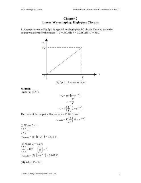
1. A ramp shown in Fig.2p.1 is applied <strong>to</strong> a high-pass RC circuit. Draw <strong>to</strong> scale the<br />
output waveform for the cases: (i) T = RC, (ii) T = 0.2RC, (iii) T = 5RC.<br />
Fig.2p.1<br />
A ramp as input<br />
Solution:<br />
From Eq. (2.64):<br />
/<br />
v o = <br />
1<br />
e t <br />
V<br />
<br />
T<br />
<br />
v o = 1<br />
e t<br />
T <br />
The peak of the output will occur at t = T. We know:<br />
<br />
v o(peak) = 1<br />
T <br />
(i) When T = :<br />
<br />
= 1<br />
T <br />
1<br />
v o (peak) = (1) 1<br />
e = 0.632 V.<br />
(ii) When T = 0.2 :<br />
T <br />
= 0.2, = 5<br />
T<br />
0.2<br />
v o (peak) = (5) 1<br />
e = 0.907 V<br />
(iii) When T = 5 :<br />
V /<br />
<br />
V /<br />
e T <br />
© 2010 Dorling Kindersley India Pvt. Ltd 1
Pulse and Digital Circuits Venkata Rao K., Rama Sudha K. and Manmadha Rao G.<br />
T <br />
= 5 = 0.2<br />
T<br />
5<br />
v o (peak) = (0.2) 1<br />
e = 0.198 V.<br />
Fig.1<br />
Response of the high-pass circuit for ramp input<br />
2. A waveform shown in Fig.2p.2 is applied as input <strong>to</strong> an RC high-pass circuit whose<br />
time constant is 250 ps. If the maximum output voltage across the resis<strong>to</strong>r is 50 V, what<br />
is the peak value of the input waveform?<br />
Fig.2p.2<br />
Input <strong>to</strong> the high-pass RC circuit<br />
Solution:<br />
For a ramp input<br />
v () t <br />
RC(1 e<br />
)<br />
o<br />
t RC<br />
At 0.005 10<br />
6<br />
t t1<br />
s<br />
v<br />
<br />
i<br />
50 25010 1e<br />
6<br />
0.00510<br />
<br />
<br />
1<br />
<br />
vi<br />
25010 1e<br />
6<br />
500.00510<br />
<br />
<br />
v (max) 1000V<br />
i<br />
6<br />
0.00510<br />
12 12<br />
25010<br />
<br />
<br />
<br />
6<br />
0.00510<br />
12 12<br />
25010<br />
<br />
<br />
<br />
© 2010 Dorling Kindersley India Pvt. Ltd 2
Pulse and Digital Circuits Venkata Rao K., Rama Sudha K. and Manmadha Rao G.<br />
For t t<br />
v<br />
o<br />
1<br />
50e<br />
t<br />
12<br />
25010<br />
v<br />
v<br />
o<br />
o<br />
50e<br />
0 V<br />
6<br />
110<br />
12<br />
25010<br />
3. A limited ramp shown in Fig.2p.3 is applied <strong>to</strong> an RC high-pass circuit of Fig.2.2 (a).<br />
The time constant of the RC circuit is 2 ms. Calculate the maximum value of output<br />
voltage and the output at the end of the input waveform.<br />
Fig.2p.3 Input <strong>to</strong> the high-pass circuit<br />
Solution:<br />
For a ramp input<br />
t<br />
RC<br />
vo<br />
( t)<br />
RC(1<br />
e )<br />
3<br />
At t = t 1 = 0.410<br />
s<br />
3<br />
0.410<br />
10<br />
3<br />
3<br />
210<br />
v ( t)<br />
210<br />
(1 e )<br />
3<br />
0.410<br />
The peak value occurs only at t = t 1 = 0.410<br />
v<br />
o<br />
(max) 9.063 V<br />
3<br />
s<br />
For t > t 1<br />
t<br />
3<br />
210<br />
v<br />
o<br />
9.063<br />
e<br />
The voltage at t = 10.4 ms is:<br />
© 2010 Dorling Kindersley India Pvt. Ltd 3
Pulse and Digital Circuits Venkata Rao K., Rama Sudha K. and Manmadha Rao G.<br />
v o<br />
9.063e<br />
3<br />
1010<br />
3<br />
210<br />
v o<br />
0.061V<br />
The voltage at t = 10.4 ms is 0.061 V. The output waveform is shown in Fig.3.<br />
Fig. 3 Output of the high-pass circuit for the given input<br />
4. The periodic waveform shown in Fig.2p.4 is applied <strong>to</strong> an RC differentiating circuit<br />
whose time constant is 10 µs. Sketch the output and calculate the maximum and<br />
minimum values of the output voltage with respect <strong>to</strong> the ground.<br />
Fig.2p.4 Periodic square wave as an input <strong>to</strong> the high-pass circuit<br />
Solution:<br />
Given T 1 =100 s , T 2 =1 s , τ = 10 s<br />
The steady-state output waveform is drawn by calculating V 1 ,<br />
1' '<br />
V , V2 and V 2<br />
.<br />
'<br />
At t 0, <br />
<br />
vo V2 andatt 0,<br />
vo<br />
V<br />
1<br />
t<br />
0 t T , v V e <br />
For 1 o 1<br />
At t = T 1<br />
For<br />
At<br />
© 2010 Dorling Kindersley India Pvt. Ltd 4
Pulse and Digital Circuits Venkata Rao K., Rama Sudha K. and Manmadha Rao G.<br />
T1<br />
100<br />
' <br />
10<br />
1 o 1 1 1<br />
At t T, v V Ve Ve 0<br />
For T t ( T T ), v V e<br />
1 1 2 o 2<br />
T2<br />
T2<br />
1<br />
' <br />
10<br />
2 o 2 2 2<br />
At t T, v V Ve Ve 0.904 V2<br />
<br />
Peak-<strong>to</strong>-peak input is 100 V.<br />
'<br />
V<br />
1<br />
V2<br />
100<br />
0 – V 2 = 100<br />
V 2 = –100 V<br />
'<br />
V<br />
1<br />
V2<br />
100<br />
V 1 + 0.904100<br />
= 100<br />
V 100<br />
0.904100<br />
9.6 V<br />
V<br />
V<br />
1<br />
<br />
'<br />
1<br />
'<br />
2<br />
V e<br />
1<br />
V e<br />
2<br />
T1<br />
<br />
T2<br />
<br />
100<br />
10<br />
9.6e<br />
V e<br />
2<br />
1<br />
10<br />
0<br />
0.904<br />
V2<br />
0.904 100<br />
90.4 V<br />
Fig. 4 Output of the high-pass circuit for the specified input<br />
5. The periodic ramp voltage as shown in Fig.2p.5 is applied <strong>to</strong> a high-pass RC circuit.<br />
Find equations from which <strong>to</strong> determine the steady-state output waveform when T 1 =T 2 =<br />
RC.<br />
Fig.5 A periodic ramp as input<br />
Solution:<br />
/<br />
v o = <br />
1<br />
e t <br />
(1)<br />
© 2010 Dorling Kindersley India Pvt. Ltd 5
Pulse and Digital Circuits Venkata Rao K., Rama Sudha K. and Manmadha Rao G.<br />
If there is an initial voltage of V 1 on C, Eq.(1) gets modified as follows:<br />
For the ramp input, the slope =<br />
t<br />
/ t<br />
<br />
v o = <br />
1<br />
e <br />
V e<br />
V .<br />
T 1<br />
<br />
1<br />
The capaci<strong>to</strong>r charges from V 1 <strong>to</strong> V 2 in time T 1 . At t = T 1 +, the capaci<strong>to</strong>r does not<br />
respond for sudden changes. Hence, the output changes <strong>to</strong> (V 2 – V). During T 2, the<br />
capaci<strong>to</strong>r blocks the dc. So the capaci<strong>to</strong>r discharges from V 3 <strong>to</strong> V 1 .<br />
Given T 1 = T 2 = <br />
At t = T 1 v () t o<br />
= V2<br />
Using (1)<br />
V 1 1<br />
T ( 1 e ) V<br />
(2)<br />
1e<br />
0.632 V 0. 367 V1<br />
V<br />
2<br />
=<br />
1<br />
T1<br />
v T ) =V 2 –V<br />
o(<br />
1<br />
V<br />
T2<br />
r<br />
1<br />
( V V<br />
) e (0.632V<br />
0.367V1<br />
1)<br />
V<br />
1<br />
(1 0.134) 0.135<br />
0.135<br />
V1 0.<br />
156V<br />
0.864<br />
V<br />
2<br />
=<br />
0.632V 0.367V1 0.632V<br />
0.367 0.156V<br />
0. 575V<br />
vo(<br />
T1)=V 2 –V = 0.575V – V = –0.425V<br />
e<br />
1<br />
© 2010 Dorling Kindersley India Pvt. Ltd 6
Pulse and Digital Circuits Venkata Rao K., Rama Sudha K. and Manmadha Rao G.<br />
Fig. 5 The changes in voltage with time<br />
6. A square wave of pulse width 2 ms and peak amplitude of 12 V as shown in Fig.2p.6 is<br />
applied <strong>to</strong> high-pass RC circuit with time constant 4 ms. Plot the first four cycles of the<br />
output waveform.<br />
T/2 = 2 ms<br />
Fig.2p.6 Symmetric square wave as an input<br />
Solution:<br />
Given T 1 = T 2 = 0.2 ms, τ = 4 ms<br />
(i) For t
Pulse and Digital Circuits Venkata Rao K., Rama Sudha K. and Manmadha Rao G.<br />
Fig.6 The output waveform<br />
7. A 20-Hz symmetric square wave referenced <strong>to</strong> 0 volts and, with a peak-<strong>to</strong>-peak<br />
amplitude of 10 V, is fed <strong>to</strong> an amplifier through the coupling network shown in Fig.<br />
2p.7. Calculate and plot the output waveform when the lower 3-dB frequency is: (i) 0.6<br />
Hz, (ii) 6 Hz and (iii) 60 Hz.<br />
Fig.2p.7 The given coupling network<br />
Solution:<br />
Given V = 10 V<br />
(i) f 1 = 0.6 Hz<br />
= RC =<br />
1 1<br />
0.265 s<br />
2<br />
f 2 (0.6)<br />
1<br />
1<br />
T = =<br />
1 = 0.05 s.<br />
f 20<br />
<br />
V 1 =<br />
T = 0.025 s.<br />
2<br />
V<br />
<br />
1<br />
e<br />
T<br />
/ 2<br />
10<br />
1 e<br />
=<br />
0.025 / 0. 265<br />
= 5.25 V.<br />
V = V 1 e<br />
'<br />
1<br />
T<br />
2<br />
0.025<br />
= 0. 265<br />
5.25e = 5.25(0.91) = 4.8 V.<br />
© 2010 Dorling Kindersley India Pvt. Ltd 8
Pulse and Digital Circuits Venkata Rao K., Rama Sudha K. and Manmadha Rao G.<br />
V 1 = –V 2 and<br />
V 1 = V 2 = 5.25 V<br />
V = <br />
'<br />
1<br />
V 2<br />
'<br />
= 4.8 V<br />
'<br />
V = '<br />
1<br />
V 2<br />
The output in this case is plotted in Fig.7.1.<br />
(ii) f 1 = 6 Hz<br />
Fig.7.1Output when f 1 = 0.6 Hz<br />
= RC =<br />
1 1<br />
0.0265 s<br />
2<br />
f 2 (6)<br />
1<br />
V 1 =<br />
V<br />
<br />
1<br />
e<br />
T<br />
/ 2<br />
10<br />
1 e<br />
=<br />
0.025 / 0. 0265<br />
= 7.20 V<br />
V = V 1 e<br />
'<br />
1<br />
T<br />
2<br />
0.025<br />
= 0. 0265<br />
7.20e = 7.20(0.389) = 2.8 V.<br />
V 1 = –V 2 and<br />
V 1 = V 2 =7.20 V<br />
V = <br />
'<br />
1<br />
V 2<br />
'<br />
= 2.8 V<br />
'<br />
V = '<br />
1<br />
V 2<br />
The output for this condition is plotted in Fig.7.2.<br />
© 2010 Dorling Kindersley India Pvt. Ltd 9
Pulse and Digital Circuits Venkata Rao K., Rama Sudha K. and Manmadha Rao G.<br />
(iii) f 1 = 60 Hz<br />
Fig.7.2 Output when f 1 = 6 Hz<br />
= RC =<br />
1 1<br />
0.00265 s<br />
2<br />
f 2 (60)<br />
1<br />
V 1 =<br />
V<br />
<br />
1<br />
e<br />
T<br />
/ 2<br />
=<br />
0.025 / 0. 00265<br />
1 e<br />
2<br />
=10.0 V<br />
V = V 1 e<br />
'<br />
1<br />
T<br />
2<br />
=10(0.00008) = 0.0008 V.<br />
V 1 = –V 2 and<br />
V 1 = V 2 =10.00 V<br />
V = <br />
'<br />
1<br />
V 2<br />
'<br />
=0.0008 V<br />
'<br />
V = '<br />
1<br />
V 2<br />
The output for this case is plotted in Fig.7.3..<br />
© 2010 Dorling Kindersley India Pvt. Ltd 10
Pulse and Digital Circuits Venkata Rao K., Rama Sudha K. and Manmadha Rao G.<br />
Fig.7.3 Output when f 1 = 60 Hz<br />
8. A square wave is applied as input <strong>to</strong> an amplifier through a coupling condenser of<br />
10 F. The amplifier has input resistance of 10 kΩ . Determine the lowest frequency if<br />
the tilt is not <strong>to</strong> exceed 10 per cent.<br />
Solution:<br />
We have P = 0.1, R = 10 kΩ and C = 10 F<br />
T<br />
Per cent tilt, P = 100 per cent<br />
2 <br />
1 1<br />
f 50 Hz<br />
3 6<br />
2 P 21010 1010 0.1<br />
f P = 1 100 per cent<br />
f<br />
f<br />
1<br />
Pf 0.1<br />
50<br />
1.59 Hz<br />
<br />
9. A pulse of 10 V amplitude and duration 1 ms is applied <strong>to</strong> a high-pass RC circuit with<br />
R = 20 k and C = 0.5 F . Plot the output waveform <strong>to</strong> scale and calculate the per cent<br />
tilt in the output.<br />
Solution:<br />
© 2010 Dorling Kindersley India Pvt. Ltd 11
Pulse and Digital Circuits Venkata Rao K., Rama Sudha K. and Manmadha Rao G.<br />
τ = RC = 10 ms<br />
For 0< t < t p<br />
v<br />
i<br />
=10 V<br />
v =10 e<br />
t 1010<br />
o<br />
3<br />
110<br />
3<br />
'<br />
At t = t p– , vo<br />
= 10<br />
10 10<br />
3<br />
V1 e 9. 05<br />
At t = t p+,<br />
v<br />
o<br />
= V 2 =<br />
'<br />
V 1<br />
3<br />
t1<br />
10 <br />
3<br />
1010<br />
V<br />
– V = 9.05 – 10 = –0.95 V<br />
For t > t p, v<br />
o<br />
= –0.95 e<br />
'<br />
V V1 10 9.05<br />
per cent tilt 100 100 9.5 per cent<br />
V<br />
10<br />
Fig. 9 The output waveform<br />
10. The input <strong>to</strong> the high-pass circuit in Fig. 2p.10 is the waveform shown in Fig. 2p.10.<br />
Calculate and plot the output waveform <strong>to</strong> scale, given that RC = τ = 0.1 ms .<br />
.<br />
Fig.2p.10 Input <strong>to</strong> the high-pass circuit<br />
Solution:<br />
© 2010 Dorling Kindersley India Pvt. Ltd 12
Pulse and Digital Circuits Venkata Rao K., Rama Sudha K. and Manmadha Rao G.<br />
For t < 0.1 ms v = 0, v = 0<br />
(i) At t = 0.1 ms, the input suddenly falls <strong>to</strong> –5 V, and the output also changes by the<br />
same amount as the capaci<strong>to</strong>r acts as a short circuit.<br />
For 0.1 < t
Pulse and Digital Circuits Venkata Rao K., Rama Sudha K. and Manmadha Rao G.<br />
Fig.10 The output waveform<br />
11. A pulse of 10-V amplitude with a pulse width of 0.5 ms, as shown in Fig.2p.9, is<br />
applied <strong>to</strong> a high-pass RC circuit of Fig. 2.1(a), having time constant 10 ms. Sketch the<br />
output waveform and determine the per cent tilt in the output.<br />
Solution:<br />
10 ms<br />
For, 0< t < t p<br />
v i<br />
=10 V<br />
=10 e<br />
t 1010<br />
v o<br />
At t = t p- , v o<br />
=<br />
3<br />
3<br />
0.510<br />
' 3<br />
1010<br />
V1 10e<br />
9.512 V<br />
'<br />
At t = t p+ , vo<br />
= V 2 = V 1<br />
–V = 9.512 – 10 = –0.488V<br />
3<br />
t0.510<br />
<br />
3<br />
10<br />
10<br />
For t > t p , vo<br />
= –0.488 e<br />
'<br />
V V1<br />
10 9.512<br />
per cent tilt 100 100 4.88 per cent<br />
V<br />
10<br />
The output is also shown in Fig. 2p.9.<br />
Fig.2p.9 Input and output of the high-pass circuit<br />
12. A high-pass RC circuit is desired <strong>to</strong> pass a 3-ms sweep (ramp input) with less than 0.4<br />
per cent transmission error. Calculate the highest possible value of the lower 3-dB<br />
frequency.<br />
Solution:<br />
Consider the circuit in Fig. 2.1(a).<br />
T = 3 10 -3 s<br />
per cent e t(max) =0.4 per cent or e t(max) = 0.004<br />
© 2010 Dorling Kindersley India Pvt. Ltd 14
Pulse and Digital Circuits Venkata Rao K., Rama Sudha K. and Manmadha Rao G.<br />
T<br />
et<br />
<br />
fT<br />
1<br />
2<br />
3<br />
0.004 <br />
f1<br />
310<br />
13. A symmetric square wave with f = 500 kHz shown<br />
0.004<br />
f1 0.4244 Hz in Fig.2p.13 is fed <strong>to</strong> an RC high-pass network of<br />
3<br />
310<br />
Fig.2.1(a). Calculate and plot the transient and the<br />
steady-state response if: (i) τ = 5T and (ii) τ = T/20.<br />
Fig.2p.13 Input <strong>to</strong> the coupling network<br />
Solution:<br />
Given f = 500 Hz, hence T = 2.0 ms.<br />
Case 1:<br />
Given, τ = 5T =10 ms.<br />
When τ is large, the capaci<strong>to</strong>r charges and discharges very slowly. The output has a<br />
small tilt. The voltages are calculated <strong>to</strong> plot the transient response.<br />
i. For t < 0, v = 0, and hence v = 0<br />
At t = 0, jumps <strong>to</strong> 150 V.<br />
As the voltage across capaci<strong>to</strong>r canno t change instantaneously, v<br />
o<br />
is also equal <strong>to</strong> 150 V.<br />
At t = 0 v<br />
o<br />
= V<br />
a<br />
= 150 V.<br />
ii. During the period 0 < t < 1.0 ms, as the input is constant the output decays.<br />
vo<br />
= V a<br />
e<br />
v i<br />
t<br />
<br />
i<br />
t<br />
o<br />
1<br />
<br />
At t = 1.0 ms, vo<br />
= Vb<br />
= V e a<br />
= 150 e 10 = 135.72 V.<br />
At t = 1.0 ms, the input falls by 100 V. The output also falls by 100 V.<br />
V = V – 100 = 135.72 – 100 = 35.72 V.<br />
c<br />
b<br />
iii. For 1.0 < t < 2.0, v = V c<br />
e<br />
o<br />
( tT<br />
/ 2)<br />
<br />
1.0<br />
10<br />
0.1<br />
At t = T = 2 ms, v o<br />
= Vd<br />
= V<br />
c<br />
e 35.72e<br />
= 32.32 V.<br />
At t = 2 ms, the input rises by 100 V. The output also rises by 100 V.<br />
V<br />
e<br />
= V<br />
d<br />
+ 100 = 32.32 + 100 = 132.32 V.<br />
© 2010 Dorling Kindersley India Pvt. Ltd 15
Pulse and Digital Circuits Venkata Rao K., Rama Sudha K. and Manmadha Rao G.<br />
iv. During the period T < t < 3T/2, that is, between 2 <strong>to</strong> 3 ms, the output decays.<br />
1.0<br />
10<br />
At t = 3 ms v<br />
o<br />
=<br />
f<br />
At 3 ms, the input falls by 100 V. Hence<br />
V g<br />
= V – 100 = 19.73 V<br />
f<br />
V = V e<br />
e = 132.32 (0.9048) = 119.73 V.<br />
v. During 3T /2 < t < 2T, that is, d uring 3 <strong>to</strong> 4 ms, the output decays.<br />
1.0<br />
10<br />
0.1<br />
At t = 2T= 4 ms, v<br />
o<br />
= V<br />
h<br />
= V g<br />
e = 19.73 e =17.85 V.<br />
V<br />
j<br />
= V<br />
h<br />
+ 100 V = 17.85+100=117.85 V.<br />
In a few cycles, the output reaches the steady state.<br />
Steady-state response:<br />
Under steady state, the output is symmetrical with respect <strong>to</strong> zero volts, since the<br />
capaci<strong>to</strong>r blocks dc. Therefore, the dc component in the output is zero.<br />
Let V 1 be the voltage at t = 0<br />
t<br />
<br />
For 0 < t < T/2, v<br />
o<br />
= V1<br />
e<br />
'<br />
0.1<br />
At t = T/2=1 ms, vo<br />
= V1<br />
= V<br />
1e<br />
= 0.905 V<br />
1<br />
'<br />
V<br />
1<br />
= 0.905 V<br />
1<br />
(3)<br />
As the input abruptly falls, output also falls by the same amount <strong>to</strong> V 2 .<br />
(tT / 2)<br />
<br />
For T/2 < t < T v<br />
o<br />
= V<br />
2<br />
e<br />
'<br />
0.1<br />
At t = T, v o<br />
= V 2 = V 2<br />
e = 0.905 V 2<br />
'<br />
V2 = 0.905 V<br />
2<br />
(4)<br />
For symmetrical wave<br />
' '<br />
V<br />
1<br />
= V 2<br />
and V<br />
1<br />
= V2<br />
(5)<br />
'<br />
'<br />
V<br />
1<br />
V2<br />
= 100 V and V1<br />
V 2<br />
= 100 V (6)<br />
'<br />
From (6), we have V1 V2<br />
= 100 V (7)<br />
And from (3), we have V1<br />
= V2<br />
(8)<br />
'<br />
Substituting (8) in (7), we have V<br />
1<br />
+ V 1<br />
= 100 V (9)<br />
'<br />
From (3), we have V<br />
1<br />
= 0.905 V<br />
1<br />
Substituting in (9)<br />
0.905V 1<br />
+ V<br />
1= 100 V<br />
1.905V 1<br />
= 100 V.<br />
'<br />
V<br />
1<br />
=52.49 V and V 1<br />
= 0.905V 1<br />
= (0.905)(52.49)= 47.50 V<br />
' '<br />
From (5) as V<br />
1<br />
= V2<br />
an d V1<br />
= V2<br />
'<br />
V 2<br />
= –52.49 V V 2<br />
= –47.50 V<br />
We can now plot the steady-state response as we know<br />
'<br />
V = 52.49 V<br />
V = 47.50 V<br />
1 1<br />
© 2010 Dorling Kindersley India Pvt. Ltd 16
Pulse and Digital Circuits Venkata Rao K., Rama Sudha K. and Manmadha Rao G.<br />
'<br />
V<br />
2<br />
= –52.49 V<br />
2<br />
V<br />
= –47.50 V<br />
The transient and steady-state responses are plotted in Figs.13.1 and<br />
13.2.<br />
Fi g.13 .1 Transient response<br />
Fig.13.2 Steady-state response<br />
Case 2:<br />
For very low time constant, i.e. when τ = T/20 = 0.1 ms.<br />
Since the time constant is very small, the capaci<strong>to</strong>r charges and discharges very fast.<br />
The input and output are shown in Fig.13.3.<br />
© 2010 Dorling Kindersley India Pvt. Ltd 17
Pulse and Digital Circuits Venkata Rao K., Rama Sudha K. and Manmadha Rao G.<br />
Fig.13.3 Output for the given input when time constant is very small<br />
14. A current pulse of amplitude 5 A in Fig.2p.11 is applied <strong>to</strong> a parallel RC combination<br />
shown in Fig.2p.12. Plot <strong>to</strong> scale the waveforms of the current flowing through capaci<strong>to</strong>r<br />
for the cases: (i) t p =0.1RC, (ii) t p = RC, (iii) t p = 5RC<br />
Fig.2p.11The given input <strong>to</strong> the circuit<br />
Fig. 2p.12 The given circuit<br />
Solution:<br />
Till t = t p , using Laplace transforms, the circuit can be drawn as in Fig.14.1.<br />
© 2010 Dorling Kindersley India Pvt. Ltd 18
Pulse and Digital Circuits Venkata Rao K., Rama Sudha K. and Manmadha Rao G.<br />
Fig.14.1 Circuit in terms of Laplace transforms<br />
Applying KCL, we have<br />
5<br />
5RCs 5<br />
IC<br />
() s R s <br />
1 RCs 1s<br />
1<br />
R <br />
<br />
s<br />
Cs<br />
<br />
RC<br />
Taking<br />
<br />
t<br />
RC<br />
Laplace inverse, the charging current is<br />
iC<br />
( t)<br />
5e<br />
At t = t p, the current suddenly falls from 5 A <strong>to</strong> 0. The voltage across the capaci<strong>to</strong>r at t =<br />
t p is [ 5 iC ( t<br />
p<br />
)] R<br />
Therefore for t ≥ t p,<br />
[5 iC( tp)] R [5 iC( tp)]<br />
IC<br />
() s <br />
<br />
1 1<br />
sR ( ) ( s<br />
)<br />
Cs RC<br />
Taking Laplaceinverse i ( t) [5 i ( t )] e<br />
C C p<br />
-t-t ( p )<br />
RC<br />
The circuit that represents the discharge of the condenser is presented in Fig.14.2.<br />
Case 1:<br />
For 0 < t < t<br />
i<br />
C<br />
p<br />
( t)<br />
5e<br />
i C decays exponentially,<br />
Fig.14.2 Circuit that indicates the discharge of the condenser<br />
t<br />
RC<br />
0.1RC<br />
RC<br />
at t t , i ( t ) 5e<br />
4.524 A<br />
p C p<br />
For t > t p , i C rises exponentially as<br />
© 2010 Dorling Kindersley India Pvt. Ltd 19
Pulse and Digital Circuits Venkata Rao K., Rama Sudha K. and Manmadha Rao G.<br />
i C = – 5 i C<br />
( t )]<br />
[<br />
p<br />
( t t p )<br />
e<br />
RC<br />
= –0.4758<br />
<br />
e<br />
t<br />
t<br />
p<br />
RC<br />
<br />
Case 2:<br />
For 0 < t < t p<br />
i<br />
i C decays exponentially,<br />
C<br />
( t)<br />
5e<br />
t<br />
RC<br />
RC<br />
RC 1<br />
at t tp, Ic( tp) 5e 5e<br />
1.839 A<br />
For t > t p i C decays exponentially as<br />
<br />
[5 I ( t )]<br />
C<br />
p<br />
e<br />
tt<br />
p<br />
<br />
RC<br />
t<br />
<br />
= –3.16 e<br />
t<br />
p<br />
RC<br />
<br />
Case 3:<br />
For 0 < t < t p<br />
i C decays exponentially, i<br />
a<br />
C<br />
( t)<br />
5e<br />
t<br />
RC<br />
5RC<br />
5<br />
t t tp, Ic( tp) 5e RC 5e 0.0336 A<br />
For t > t p i C rises exponentially as<br />
t<br />
t<br />
p <br />
t<br />
t<br />
p <br />
<br />
<br />
RC<br />
RC<br />
–[5 i C<br />
( t p<br />
)] e = –4.966 e<br />
The input and outputs are plotted in Fig.14.3.<br />
© 2010 Dorling Kindersley India Pvt. Ltd 20
Pulse and Digital Circuits Venkata Rao K., Rama Sudha K. and Manmadha Rao G.<br />
Fig.14.3 Input and outputs for the given circuit<br />
15. Draw the output waveform if the waveform shown in Fig.2p.15(a) is applied at the<br />
input of the RC circuit shown in Fig.2p.15(b).<br />
© 2010 Dorling Kindersley India Pvt. Ltd 21
Pulse and Digital Circuits Venkata Rao K., Rama Sudha K. and Manmadha Rao G.<br />
Fig.2p.15(a) The input <strong>to</strong> the high-pass circuit in Fig.2p.15(a)<br />
Solution:<br />
Fig.2p.15(b) The given high-pass circuit<br />
Timeconstatnt RC<br />
1001010<br />
9<br />
9<br />
100010<br />
s<br />
Time period of input waveform is<br />
T = 4 ms<br />
Since RC
Pulse and Digital Circuits Venkata Rao K., Rama Sudha K. and Manmadha Rao G.<br />
100 3<br />
For 2 < t < 4 ms, v i<br />
( t 2 10<br />
)<br />
3<br />
2 10<br />
9 d 100<br />
<br />
3<br />
vo 100010 ( t 2 10 )<br />
3<br />
<br />
dt 210<br />
<br />
9<br />
( 100)<br />
100010 50 mV<br />
3<br />
210<br />
The output waveform is shown in Fig. 15..<br />
Fig.15 Output of the high-pass circuit<br />
© 2010 Dorling Kindersley India Pvt. Ltd 23


![[Productnaam] Marketingplan - Pearson](https://img.yumpu.com/26285712/1/190x132/productnaam-marketingplan-pearson.jpg?quality=85)