

An Analysis of Contact Resistance between Probe Tip and Gold Pad
An Analysis of Contact Resistance between Probe Tip and Gold Pad
An Analysis of Contact Resistance between Probe Tip and Gold Pad

Create successful ePaper yourself
Turn your PDF publications into a flip-book with our unique Google optimized e-Paper software.
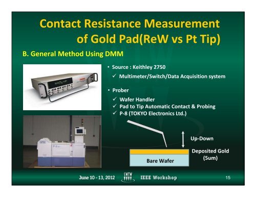
<strong>Contact</strong> <strong>Resistance</strong> Measurement<br />
B. General Method Using DMM<br />
<strong>of</strong> <strong>Gold</strong> <strong>Pad</strong>(ReW vs Pt <strong>Tip</strong>)<br />
• Source : Keithley 2750<br />
Multimeter/Switch/Data Acquisition system<br />
• <strong>Probe</strong>r<br />
Wafer H<strong>and</strong>ler<br />
<strong>Pad</strong> to <strong>Tip</strong> Automatic <strong>Contact</strong> & Probing<br />
P‐8 (TOKYO Electronics Ltd.)<br />
Up‐Down<br />
Bare Wafer<br />
Deposited <strong>Gold</strong><br />
(5um)<br />
15


