

An Analysis of Contact Resistance between Probe Tip and Gold Pad
An Analysis of Contact Resistance between Probe Tip and Gold Pad
An Analysis of Contact Resistance between Probe Tip and Gold Pad

You also want an ePaper? Increase the reach of your titles
YUMPU automatically turns print PDFs into web optimized ePapers that Google loves.
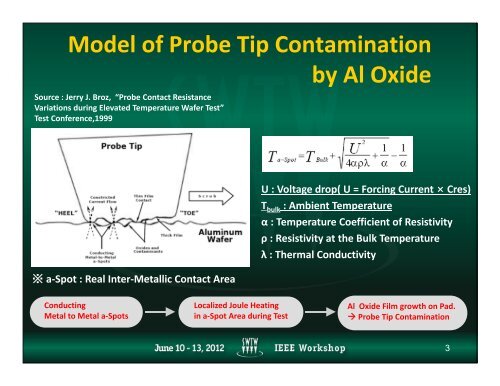
Model <strong>of</strong> <strong>Probe</strong> <strong>Tip</strong> Contamination<br />
Source : Jerry J. Broz, “<strong>Probe</strong> <strong>Contact</strong> <strong>Resistance</strong><br />
Variations during Elevated Temperature Wafer Test”<br />
Test Conference,1999<br />
by Al Oxide<br />
U : Voltage drop( U = Forcing Current × Cres)<br />
T bulk : Ambient Temperature<br />
α : Temperature Coefficient <strong>of</strong> Resistivity<br />
ρ : Resistivity at the Bulk Temperature<br />
λ : Thermal Conductivity<br />
※ a‐Spot : Real Inter‐Metallic <strong>Contact</strong> Area<br />
Conducting<br />
Metal to Metal a‐Spots<br />
Localized Joule Heating<br />
in a‐Spot Area during Test<br />
Al Oxide Film growth on <strong>Pad</strong>.<br />
<strong>Probe</strong> <strong>Tip</strong> Contamination<br />
3


