

High Speed 3D Probe Mark Inspection - Semiconductor Wafer Test ...
High Speed 3D Probe Mark Inspection - Semiconductor Wafer Test ...
High Speed 3D Probe Mark Inspection - Semiconductor Wafer Test ...

Create successful ePaper yourself
Turn your PDF publications into a flip-book with our unique Google optimized e-Paper software.
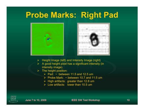
<strong>Probe</strong> <strong>Mark</strong>s: Right Pad<br />
‣ Height Image (left) and Intensity Image (right)<br />
‣ A good height pixel has a significant intensity (in<br />
intensity image).<br />
‣ The height position:<br />
‣ Pad: ~ between 11.5 and 12.5 um<br />
‣ <strong>Probe</strong> <strong>Mark</strong>: ~ between 10.7 and 11.5 um<br />
‣ <strong>High</strong> artifacts: greater than 12.8 um<br />
‣ Low artifacts: lower than 10.5 um<br />
June 7 to 10, 2009<br />
IEEE SW <strong>Test</strong> Workshop 10


