

High Speed 3D Probe Mark Inspection - Semiconductor Wafer Test ...
High Speed 3D Probe Mark Inspection - Semiconductor Wafer Test ...
High Speed 3D Probe Mark Inspection - Semiconductor Wafer Test ...

Create successful ePaper yourself
Turn your PDF publications into a flip-book with our unique Google optimized e-Paper software.
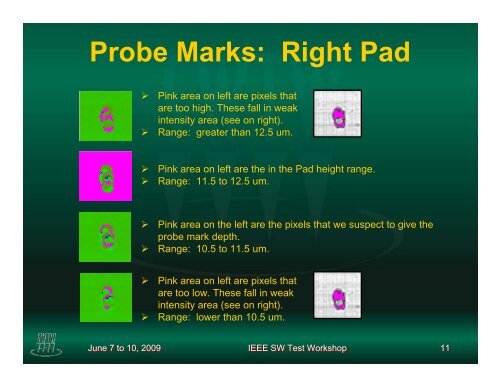
<strong>Probe</strong> <strong>Mark</strong>s: Right Pad<br />
‣ Pink area on left are pixels that<br />
are too high. These fall in weak<br />
intensity area (see on right).<br />
‣ Range: greater than 12.5 um.<br />
‣ Pink area on left are the in the Pad height range.<br />
‣ Range: 11.5 to 12.5 um.<br />
‣ Pink area on the left are the pixels that we suspect to give the<br />
probe mark depth.<br />
‣ Range: 10.5 to 11.5 um.<br />
‣ Pink area on left are pixels that<br />
are too low. These fall in weak<br />
intensity area (see on right).<br />
‣ Range: lower than 10.5 um.<br />
June 7 to 10, 2009<br />
IEEE SW <strong>Test</strong> Workshop 11


