

High Speed 3D Probe Mark Inspection - Semiconductor Wafer Test ...
High Speed 3D Probe Mark Inspection - Semiconductor Wafer Test ...
High Speed 3D Probe Mark Inspection - Semiconductor Wafer Test ...

You also want an ePaper? Increase the reach of your titles
YUMPU automatically turns print PDFs into web optimized ePapers that Google loves.
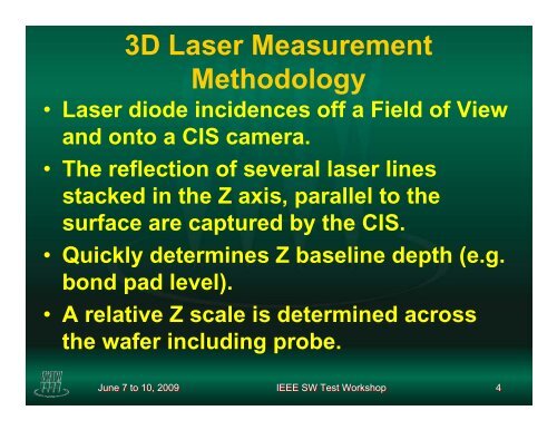
<strong>3D</strong> Laser Measurement<br />
Methodology<br />
• Laser diode incidences off a Field of View<br />
and onto a CIS camera.<br />
• The reflection of several laser lines<br />
stacked in the Z axis, parallel to the<br />
surface are captured by the CIS.<br />
• Quickly determines Z baseline depth (e.g.<br />
bond pad level).<br />
• A relative Z scale is determined across<br />
the wafer including probe.<br />
June 7 to 10, 2009<br />
IEEE SW <strong>Test</strong> Workshop 4


