

High Speed 3D Probe Mark Inspection - Semiconductor Wafer Test ...
High Speed 3D Probe Mark Inspection - Semiconductor Wafer Test ...
High Speed 3D Probe Mark Inspection - Semiconductor Wafer Test ...
SHOW LESS

You also want an ePaper? Increase the reach of your titles
YUMPU automatically turns print PDFs into web optimized ePapers that Google loves.
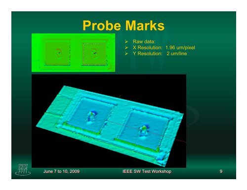
<strong>Probe</strong> <strong>Mark</strong>s<br />
‣ Raw data:<br />
‣ X Resolution: 1.96 um/pixel<br />
‣ Y Resolution: 2 um/line<br />
June 7 to 10, 2009<br />
IEEE SW <strong>Test</strong> Workshop 9


