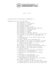
vulcan-cryptanalysis
vulcan-cryptanalysis
vulcan-cryptanalysis

You also want an ePaper? Increase the reach of your titles
YUMPU automatically turns print PDFs into web optimized ePapers that Google loves.
Pin 2 is cryptovariable input. It conveys the cryptovariable from the key<br />
loader to the IC during key loading operations. It is connected directly to the<br />
CV shift register seen at the far right of the chip.<br />
Pin 3 is plaintext input. It connects to some switching logic near the top center<br />
of the die. The switching logic routes plaintext and ciphertext to the appropriate<br />
circuits depending on whether the chip is operating in encrypt (transmit)<br />
or decrypt (receive) mode.<br />
Pin 4 is TX/RX input. It selects whether the chip encrypts (TX) or decrypts<br />
(RX). This signal connects to the same switching logic circuitry as Pin 3.<br />
Pin 5 is ciphertext input. It connects to a differential decoder and then to<br />
the switching circuitry that routes it appropriately based on whether the chip<br />
is encrypting or decrypting.<br />
The un-bonded pin between Pin 5 and Pin 6 is a test output that is inaccessible<br />
external to the chip. This test pin allows the contents of the 128-bit SRAM<br />
(discussed later) to be read, presumably to enable testing of the SRAM during<br />
manufacturing. We have deliberately chosen not to give this pin a number since<br />
it has no function during normal operation.<br />
Pin 6 is V+, the positive supply voltage. It supplies Vdd to all the transistors<br />
on the chip.<br />
Pin 7 is ciphertext output. It is differentially encoded and is valid only<br />
during encrypt (transmit) operations.<br />
Pin 8 is clock input. It allows an externally sourced clock signal to act as a<br />
time base for all synchronous logic on the chip. External inputs to the chip are<br />
clocked in on the rising edge of this clock. The nominal clock rate should be 12<br />
KHz during encrypt and decrypt operations, but we observe that the DVP key<br />
loader supplies a faster clock than this during key loading.<br />
Pin 9 is WE (write enable) input. When active (low), it allows the CV shift<br />
register to operate, clocking in CV bits from Pin 2 in accordance with the clock<br />
signal on Pin 8. Circuitry on the chip creates a single clock cycle delay between<br />
the WE input and the clock and CV inputs, an observation that is important<br />
when analyzing the exact temporal relationship of these three signals.<br />
Pin 10 is output-enable input. This signal must be high in order for ciphertext<br />
out (Pin 7) and plaintext out (Pin 11) to produce outputs. If Pin 10 is low,<br />
ciphertext out and plaintext out will be in high impedance states.<br />
Pin 11 is plaintext output. It connects to the bottom of the XOR tree and<br />
is only valid during decrypt operations.<br />
Pint 12 is ground. It provides Vss to all the transistors on the chip.<br />
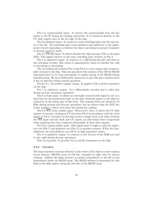
2.2.2 Circuitry<br />
The large repetitive structure directly in the center of the chip is a static random<br />
access memory (SRAM) array of 128 bits, arranged as eight rows by sixteen<br />
columns. Address decoding circuitry is present immediately to the left of and<br />
immediately below the SRAM array. The SRAM address is determined by bits<br />
held in the shift register along the left side of the SRAM array.<br />
10