GAL16V8 - Soemtron.org
GAL16V8 - Soemtron.org
GAL16V8 - Soemtron.org

You also want an ePaper? Increase the reach of your titles
YUMPU automatically turns print PDFs into web optimized ePapers that Google loves.
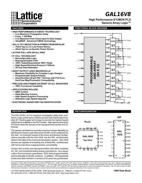
Specifications <strong>GAL16V8</strong><br />
<strong>GAL16V8</strong><br />
High Performance E 2 CMOS PLD<br />
Generic Array Logic<br />
FEATURES<br />
FUNCTIONAL BLOCK DIAGRAM<br />
• HIGH PERFORMANCE E 2 CMOS ® TECHNOLOGY<br />
— 5 ns Maximum Propagation Delay<br />
— Fmax = 166 MHz<br />
— 4 ns Maximum from Clock Input to Data Output<br />
— UltraMOS ® Advanced CMOS Technology<br />
I/CLK<br />
CLK<br />
8 OLMC<br />
I/O/Q<br />
• 50% to 75% REDUCTION IN POWER FROM BIPOLAR<br />
— 75mA Typ Icc on Low Power Device<br />
— 45mA Typ Icc on Quarter Power Device<br />
I<br />
8<br />
OLMC<br />
I/O/Q<br />
• ACTIVE PULL-UPS ON ALL PINS<br />
I<br />
•E 2 CELL TECHNOLOGY<br />
— Reconfigurable Logic<br />
— Reprogrammable Cells<br />
— 100% Tested/Guaranteed 100% Yields<br />
— High Speed Electrical Erasure (
Specifications <strong>GAL16V8</strong><br />
<strong>GAL16V8</strong> ORDERING INFORMATION<br />
Commercial Grade Specifications<br />
T pd (ns) T su (ns)<br />
T co (ns)<br />
I cc (mA)<br />
Ordering<br />
#<br />
5 3 4 115<br />
<strong>GAL16V8</strong>C-5LP<br />
115<br />
<strong>GAL16V8</strong>C-5LJ<br />
20-Pin Plastic DIP<br />
20-Lead PLCC<br />
Package<br />
7.5<br />
7 5 115<br />
<strong>GAL16V8</strong>C-7LP<br />
20-Pin Plastic DIP<br />
115<br />
<strong>GAL16V8</strong>C-7LJ<br />
20-Lead PLCC<br />
115<br />
<strong>GAL16V8</strong>B-7LP<br />
115<br />
<strong>GAL16V8</strong>B-7LJ<br />
10<br />
10<br />
7 115<br />
<strong>GAL16V8</strong>B-10LP<br />
115<br />
<strong>GAL16V8</strong>B-10LJ<br />
15<br />
12<br />
10<br />
55<br />
<strong>GAL16V8</strong>B-15QP<br />
55<br />
<strong>GAL16V8</strong>B-15QJ<br />
20-Pin Plastic DIP<br />
20-Lead PLCC<br />
20-Pin Plastic DIP<br />
20-Lead PLCC<br />
20-Pin Plastic DIP<br />
20-Lead PLCC<br />
90<br />
<strong>GAL16V8</strong>B-15LP<br />
90<br />
<strong>GAL16V8</strong>B-15LJ<br />
25<br />
15<br />
12<br />
55<br />
<strong>GAL16V8</strong>B-25QP<br />
55<br />
<strong>GAL16V8</strong>B-25QJ<br />
90<br />
<strong>GAL16V8</strong>B-25LP<br />
90<br />
<strong>GAL16V8</strong>B-25LJ<br />
20-Pin Plastic DIP<br />
20-Lead PLCC<br />
20-Pin Plastic DIP<br />
20-Lead PLCC<br />
20-Pin Plastic DIP<br />
20-Lead PLCC<br />
Industrial Grade Specifications<br />
T pd (ns) T su (ns)<br />
T co (ns)<br />
I cc (mA)<br />
Ordering<br />
#<br />
7.5<br />
7 5 130<br />
<strong>GAL16V8</strong>C-7LPI<br />
130<br />
<strong>GAL16V8</strong>C-7LJI<br />
10<br />
10<br />
7 130<br />
<strong>GAL16V8</strong>B-10LPI<br />
130<br />
<strong>GAL16V8</strong>B-10LJI<br />
15<br />
12<br />
10<br />
130<br />
<strong>GAL16V8</strong>B-15LPI<br />
130<br />
<strong>GAL16V8</strong>B-15LJI<br />
20<br />
13<br />
11<br />
65<br />
<strong>GAL16V8</strong>B-20QPI<br />
65<br />
<strong>GAL16V8</strong>B-20QJI<br />
25<br />
15<br />
12<br />
65<br />
<strong>GAL16V8</strong>B-25QPI<br />
65<br />
<strong>GAL16V8</strong>B-25QJI<br />
130<br />
<strong>GAL16V8</strong>B-25LPI<br />
130<br />
<strong>GAL16V8</strong>B-25LJI<br />
20-Pin Plastic DIP<br />
20-Lead PLCC<br />
20-Pin Plastic DIP<br />
20-Lead PLCC<br />
20-Pin Plastic DIP<br />
20-Lead PLCC<br />
20-Pin Plastic DIP<br />
20-Lead PLCC<br />
20-Pin Plastic DIP<br />
20-Lead PLCC<br />
20-Pin Plastic DIP<br />
20-Lead PLCC<br />
Package<br />
PART NUMBER DESCRIPTION<br />
_<br />
XXXXXXXX XX X X X<br />
<strong>GAL16V8</strong>C<br />
<strong>GAL16V8</strong>B<br />
Device Name<br />
Speed (ns)<br />
Grade<br />
Blank = Commercial<br />
I = Industrial<br />
L = Low Power<br />
Q = Quarter Power<br />
Power<br />
Package<br />
P = Plastic DIP<br />
J = PLCC<br />
3-66<br />
1996 Data Book
Specifications <strong>GAL16V8</strong><br />
OUTPUT LOGIC MACROCELL (OLMC)<br />
The following discussion pertains to configuring the output logic<br />
macrocell. It should be noted that actual implementation is accomplished<br />
by development software/hardware and is completely<br />
transparent to the user.<br />
There are three global OLMC configuration modes possible:<br />
simple, complex, and registered. Details of each of these<br />
modes are illustrated in the following pages. Two global bits, SYN<br />
and AC0, control the mode configuration for all macrocells. The<br />
XOR bit of each macrocell controls the polarity of the output in any<br />
of the three modes, while the AC1 bit of each of the macrocells<br />
controls the input/output configuration. These two global and 16<br />
individual architecture bits define all possible configurations in a<br />
<strong>GAL16V8</strong> . The information given on these architecture bits is<br />
only to give a better understanding of the device. Compiler software<br />
will transparently set these architecture bits from the pin<br />
definitions, so the user should not need to directly manipulate<br />
these architecture bits.<br />
The following is a list of the PAL architectures that the <strong>GAL16V8</strong><br />
can emulate. It also shows the OLMC mode under which the<br />
<strong>GAL16V8</strong> emulates the PAL architecture.<br />
PAL Architectures<br />
Emulated by <strong>GAL16V8</strong><br />
16R8<br />
16R6<br />
16R4<br />
16RP8<br />
16RP6<br />
16RP4<br />
16L8<br />
16H8<br />
16P8<br />
10L8<br />
12L6<br />
14L4<br />
16L2<br />
10H8<br />
12H6<br />
14H4<br />
16H2<br />
10P8<br />
12P6<br />
14P4<br />
16P2<br />
<strong>GAL16V8</strong><br />
Global OLMC Mode<br />
Registered<br />
Registered<br />
Registered<br />
Registered<br />
Registered<br />
Registered<br />
Complex<br />
Complex<br />
Complex<br />
Simple<br />
Simple<br />
Simple<br />
Simple<br />
Simple<br />
Simple<br />
Simple<br />
Simple<br />
Simple<br />
Simple<br />
Simple<br />
Simple<br />
COMPILER SUPPORT FOR OLMC<br />
Software compilers support the three different global OLMC<br />
modes as different device types. These device types are listed<br />
in the table below. Most compilers have the ability to automatically<br />
select the device type, generally based on the register usage<br />
and output enable (OE) usage. Register usage on the device<br />
forces the software to choose the registered mode. All combinatorial<br />
outputs with OE controlled by the product term will force the<br />
software to choose the complex mode. The software will choose<br />
the simple mode only when all outputs are dedicated combinatorial<br />
without OE control. The different device types listed in the table<br />
can be used to override the automatic device selection by the<br />
software. For further details, refer to the compiler software<br />
manuals.<br />
In registered mode pin 1 and pin 11 are permanently configured<br />
as clock and output enable, respectively. These pins cannot be<br />
configured as dedicated inputs in the registered mode.<br />
In complex mode pin 1 and pin 11 become dedicated inputs and<br />
use the feedback paths of pin 19 and pin 12 respectively. Because<br />
of this feedback path usage, pin 19 and pin 12 do not have the<br />
feedback option in this mode.<br />
In simple mode all feedback paths of the output pins are routed<br />
via the adjacent pins. In doing so, the two inner most pins ( pins<br />
15 and 16) will not have the feedback option as these pins are<br />
always configured as dedicated combinatorial output.<br />
When using compiler software to configure the device, the user<br />
must pay special attention to the following restrictions in each<br />
mode.<br />
Registered Complex Simple Auto Mode Select<br />
ABEL P16V8R P16V8C P16V8AS P16V8<br />
CUPL G16V8MS G16V8MA G16V8AS G16V8<br />
LOG/iC <strong>GAL16V8</strong>_R <strong>GAL16V8</strong>_C7 <strong>GAL16V8</strong>_C8 <strong>GAL16V8</strong><br />
OrCAD-PLD "Registered" 1 "Complex" 1 "Simple" 1 <strong>GAL16V8</strong>A<br />
PLDesigner P16V8R 2 P16V8C 2 P16V8C 2 P16V8A<br />
TANGO-PLD G16V8R G16V8C G16V8AS 3 G16V8<br />
1) Used with Configuration keyword.<br />
2) Prior to Version 2.0 support.<br />
3) Supported on Version 1.20 or later.<br />
3-67<br />
1996 Data Book
Specifications <strong>GAL16V8</strong><br />
REGISTERED MODE<br />
In the Registered mode, macrocells are configured as dedicated<br />
registered outputs or as I/O functions.<br />
Architecture configurations available in this mode are similar to<br />
the common 16R8 and 16RP4 devices with various permutations<br />
of polarity, I/O and register placement.<br />
All registered macrocells share common clock and output enable<br />
control pins. Any macrocell can be configured as registered or<br />
I/O. Up to eight registers or up to eight I/O's are possible in this<br />
mode. Dedicated input or output functions can be implemented<br />
as subsets of the I/O function.<br />
Registered outputs have eight product terms per output. I/O's<br />
have seven product terms per output.<br />
The JEDEC fuse numbers, including the User Electronic Signature<br />
(UES) fuses and the Product Term Disable (PTD) fuses, are<br />
shown on the logic diagram on the following page.<br />
CLK<br />
Registered Configuration for Registered Mode<br />
XOR<br />
D<br />
Q<br />
Q<br />
- SYN=0.<br />
- AC0=1.<br />
- XOR=0 defines Active Low Output.<br />
- XOR=1 defines Active High Output.<br />
- AC1=0 defines this output configuration.<br />
- Pin 1 controls common CLK for the registered outputs.<br />
- Pin 11 controls common OE for the registered outputs.<br />
- Pin 1 & Pin 11 are permanently configured as CLK &<br />
OE.<br />
OE<br />
Combinatorial Configuration for Registered Mode<br />
XOR<br />
- SYN=0.<br />
- AC0=1.<br />
- XOR=0 defines Active Low Output.<br />
- XOR=1 defines Active High Output.<br />
- AC1=1 defines this output configuration.<br />
- Pin 1 & Pin 11 are permanently configured as CLK &<br />
OE.<br />
Note: The development software configures all of the architecture control bits and checks for proper pin usage automatically.<br />
3-68<br />
1996 Data Book
Specifications <strong>GAL16V8</strong><br />
REGISTERED MODE LOGIC DIAGRAM<br />
DIP & PLCC Package Pinouts<br />
1<br />
2128<br />
0 4 8 12 16 20 24 28 PTD<br />
0000<br />
OLMC<br />
19<br />
2<br />
0224<br />
XOR-2048<br />
AC1-2120<br />
0256<br />
OLMC<br />
18<br />
3<br />
0480<br />
XOR-2049<br />
AC1-2121<br />
0512<br />
OLMC<br />
17<br />
4<br />
0736<br />
XOR-2050<br />
AC1-2122<br />
0768<br />
OLMC<br />
16<br />
5<br />
0992<br />
XOR-2051<br />
AC1-2123<br />
1024<br />
OLMC<br />
15<br />
6<br />
1248<br />
XOR-2052<br />
AC1-2124<br />
1280<br />
OLMC<br />
14<br />
7<br />
1504<br />
XOR-2053<br />
AC1-2125<br />
1536<br />
OLMC<br />
13<br />
8<br />
1760<br />
XOR-2054<br />
AC1-2126<br />
1792<br />
OLMC<br />
12<br />
9<br />
2016<br />
2191<br />
XOR-2055<br />
AC1-2127<br />
OE<br />
11<br />
SYN-2192<br />
AC0-2193<br />
3-69<br />
1996 Data Book
Specifications <strong>GAL16V8</strong><br />
COMPLEX MODE<br />
In the Complex mode, macrocells are configured as output only<br />
or I/O functions.<br />
Architecture configurations available in this mode are similar to<br />
the common 16L8 and 16P8 devices with programmable polarity<br />
in each macrocell.<br />
Up to six I/O's are possible in this mode. Dedicated inputs or<br />
outputs can be implemented as subsets of the I/O function. The<br />
two outer most macrocells (pins 12 & 19) do not have input capability.<br />
Designs requiring eight I/O's can be implemented in the<br />
Registered mode.<br />
All macrocells have seven product terms per output. One product<br />
term is used for programmable output enable control. Pins 1 and<br />
11 are always available as data inputs into the AND array.<br />
The JEDEC fuse numbers including the UES fuses and PTD fuses<br />
are shown on the logic diagram on the following page.<br />
Combinatorial I/O Configuration for Complex Mode<br />
XOR<br />
- SYN=1.<br />
- AC0=1.<br />
- XOR=0 defines Active Low Output.<br />
- XOR=1 defines Active High Output.<br />
- AC1=1.<br />
- Pin 13 through Pin 18 are configured to this function.<br />
Combinatorial Output Configuration for Complex Mode<br />
XOR<br />
- SYN=1.<br />
- AC0=1.<br />
- XOR=0 defines Active Low Output.<br />
- XOR=1 defines Active High Output.<br />
- AC1=1.<br />
- Pin 12 and Pin 19 are configured to this function.<br />
Note: The development software configures all of the architecture control bits and checks for proper pin usage automatically.<br />
3-70<br />
1996 Data Book
Specifications <strong>GAL16V8</strong><br />
COMPLEX MODE LOGIC DIAGRAM<br />
DIP & PLCC Package Pinouts<br />
1<br />
0<br />
4<br />
8<br />
12<br />
16<br />
20<br />
24<br />
28<br />
PTD<br />
2128<br />
2<br />
0000<br />
0224<br />
OLMC<br />
XOR-2048<br />
AC1-2120<br />
19<br />
0256<br />
3<br />
0480<br />
OLMC<br />
XOR-2049<br />
AC1-2121<br />
18<br />
0512<br />
4<br />
0736<br />
OLMC<br />
XOR-2050<br />
AC1-2122<br />
17<br />
5<br />
0768<br />
0992<br />
OLMC<br />
XOR-2051<br />
AC1-2123<br />
16<br />
6<br />
1024<br />
1248<br />
OLMC<br />
XOR-2052<br />
AC1-2124<br />
15<br />
7<br />
1280<br />
1504<br />
OLMC<br />
XOR-2053<br />
AC1-2125<br />
14<br />
8<br />
1536<br />
1760<br />
OLMC<br />
XOR-2054<br />
AC1-2126<br />
13<br />
9<br />
1792<br />
2016<br />
OLMC<br />
XOR-2055<br />
AC1-2127<br />
12<br />
11<br />
2191<br />
SYN-2192<br />
AC0-2193<br />
3-71<br />
1996 Data Book
Specifications <strong>GAL16V8</strong><br />
SIMPLE MODE<br />
In the Simple mode, macrocells are configured as dedicated inputs<br />
or as dedicated, always active, combinatorial outputs.<br />
Architecture configurations available in this mode are similar to<br />
the common 10L8 and 12P6 devices with many permutations of<br />
generic output polarity or input choices.<br />
Pins 1 and 11 are always available as data inputs into the AND<br />
array. The center two macrocells (pins 15 & 16) cannot be used<br />
as input or I/O pins, and are only available as dedicated outputs.<br />
The JEDEC fuse numbers including the UES fuses and PTD fuses<br />
are shown on the logic diagram.<br />
All outputs in the simple mode have a maximum of eight product<br />
terms that can control the logic. In addition, each output has programmable<br />
polarity.<br />
Vcc<br />
Combinatorial Output with Feedback Configuration<br />
for Simple Mode<br />
XOR<br />
- SYN=1.<br />
- AC0=0.<br />
- XOR=0 defines Active Low Output.<br />
- XOR=1 defines Active High Output.<br />
- AC1=0 defines this configuration.<br />
- All OLMC except pins 15 & 16 can be configured to<br />
this function.<br />
XOR<br />
Vcc<br />
Combinatorial Output Configuration for Simple Mode<br />
- SYN=1.<br />
- AC0=0.<br />
- XOR=0 defines Active Low Output.<br />
- XOR=1 defines Active High Output.<br />
- AC1=0 defines this configuration.<br />
- Pins 15 & 16 are permanently configured to this<br />
function.<br />
Dedicated Input Configuration for Simple Mode<br />
- SYN=1.<br />
- AC0=0.<br />
- XOR=0 defines Active Low Output.<br />
- XOR=1 defines Active High Output.<br />
- AC1=1 defines this configuration.<br />
- All OLMC except pins 15 & 16 can be configured to<br />
this function.<br />
Note: The development software configures all of the architecture control bits and checks for proper pin usage automatically.<br />
3-72<br />
1996 Data Book
Specifications <strong>GAL16V8</strong><br />
SIMPLE MODE LOGIC DIAGRAM<br />
DIP & PLCC Package Pinouts<br />
1<br />
0<br />
4<br />
8<br />
12<br />
16<br />
20<br />
24<br />
28<br />
PTD<br />
2128<br />
2<br />
0000<br />
0224<br />
OLMC<br />
XOR-2048<br />
AC1-2120<br />
19<br />
3<br />
0256<br />
0480<br />
OLMC<br />
XOR-2049<br />
AC1-2121<br />
18<br />
4<br />
0512<br />
0736<br />
OLMC<br />
XOR-2050<br />
AC1-2122<br />
17<br />
5<br />
0768<br />
0992<br />
OLMC<br />
XOR-2051<br />
AC1-2123<br />
16<br />
6<br />
1024<br />
1248<br />
OLMC<br />
XOR-2052<br />
AC1-2124<br />
15<br />
7<br />
1280<br />
1504<br />
OLMC<br />
XOR-2053<br />
AC1-2125<br />
14<br />
8<br />
1536<br />
1760<br />
OLMC<br />
XOR-2054<br />
AC1-2126<br />
13<br />
9<br />
1792<br />
2016<br />
OLMC<br />
XOR-2055<br />
AC1-2127<br />
12<br />
11<br />
2191<br />
SYN-2192<br />
AC0-2193<br />
3-73<br />
1996 Data Book
Specifications <strong>GAL16V8</strong>C<br />
ABSOLUTE MAXIMUM RATINGS (1) RECOMMENDED OPERATING COND.<br />
Supply voltage V CC<br />
....................................... –0.5 to +7V<br />
Input voltage applied .......................... –2.5 to V CC<br />
+1.0V<br />
Off-state output voltage applied .......... –2.5 to V CC<br />
+1.0V<br />
Storage Temperature ................................. –65 to 150°C<br />
Ambient Temperature with<br />
Power Applied ........................................ –55 to 125°C<br />
1.Stresses above those listed under the “Absolute Maximum<br />
Ratings” may cause permanent damage to the device. These<br />
are stress only ratings and functional operation of the device<br />
at these or at any other conditions above those indicated in the<br />
operational sections of this specification is not implied (while<br />
programming, follow the programming specifications).<br />
Commercial Devices:<br />
Ambient Temperature (T A<br />
) ............................... 0 to 75°C<br />
Supply voltage (V CC<br />
)<br />
with Respect to Ground ..................... +4.75 to +5.25V<br />
Industrial Devices:<br />
Ambient Temperature (T A<br />
) ...........................–40 to 85°C<br />
Supply voltage (V CC<br />
)<br />
with Respect to Ground ..................... +4.50 to +5.50V<br />
DC ELECTRICAL CHARACTERISTICS<br />
Over Recommended Operating Conditions (Unless Otherwise Specified)<br />
SYMBOL PARAMETER CONDITION MIN. TYP. 3 MAX. UNITS<br />
VIL Input Low Voltage Vss – 0.5 — 0.8 V<br />
VIH Input High Voltage 2.0 — Vcc+1 V<br />
IIL 1 Input or I/O Low Leakage Current 0V ≤ VIN ≤ VIL (MAX.) — — –100 µA<br />
IIH Input or I/O High Leakage Current 3.5V ≤ VIN ≤ VCC — — 10 µA<br />
VOL Output Low Voltage IOL = MAX. Vin = VIL or VIH — — 0.5 V<br />
VOH Output High Voltage IOH = MAX. Vin = VIL or VIH 2.4 — — V<br />
IOL Low Level Output Current — — 16 mA<br />
IOH High Level Output Current — — –3.2 mA<br />
IOS 2 Output Short Circuit Current VCC = 5V VOUT = 0.5V T A<br />
= 25°C –30 — –150 mA<br />
COMMERCIAL<br />
ICC Operating Power VIL = 0.5V VIH = 3.0V L -5/-7 — 75 115 mA<br />
Supply Current ftoggle = 15MHz Outputs Open<br />
INDUSTRIAL<br />
ICC Operating Power VIL = 0.5V VIH = 3.0V L -7 — 75 130 mA<br />
Supply Current ftoggle = 15MHz Outputs Open<br />
1) The leakage current is due to the internal pull-up resistor on all pins. See Input Buffer section for more information.<br />
2) One output at a time for a maximum duration of one second. Vout = 0.5V was selected to avoid test problems caused by tester<br />
ground degradation. Guaranteed but not 100% tested.<br />
3) Typical values are at Vcc = 5V and TA = 25 °C<br />
3-74<br />
1996 Data Book
Specifications <strong>GAL16V8</strong>C<br />
AC SWITCHING CHARACTERISTICS<br />
Over Recommended Operating Conditions<br />
COM COM IND<br />
PARAMETER<br />
TEST<br />
-5 -7 -7<br />
DESCRIPTION<br />
COND 1 .<br />
MIN. MAX. MIN. MAX. MIN. MAX.<br />
UNITS<br />
tpd A Input or I/O to 8 outputs switching 1 5 3 7.5 1 7.5 ns<br />
Comb. Output 1 output switching — — — 7 — — ns<br />
tco A Clock to Output Delay 1 4 2 5 1 5 ns<br />
tcf 2 — Clock to Feedback Delay — 3 — 3 — 3 ns<br />
tsu — Setup Time, Input or Feedback before Clock↑ 3 — 7 — 7 — ns<br />
th — Hold Time, Input or Feedback after Clock↑ 0 — 0 — 0 — ns<br />
A Maximum Clock Frequency with 142.8 — 83.3 — 83.3 — MHz<br />
External Feedback, 1/(tsu + tco)<br />
fmax 3 A Maximum Clock Frequency with 166 — 100 — 100 — MHz<br />
Internal Feedback, 1/(tsu + tcf)<br />
A Maximum Clock Frequency with 166 — 100 — 100 — MHz<br />
No Feedback<br />
twh — Clock Pulse Duration, High 3 — 5 — 5 — ns<br />
twl — Clock Pulse Duration, Low 3 — 5 — 5 — ns<br />
ten B Input or I/O to Output Enabled 1 6 3 9 1 9 ns<br />
B OE to Output Enabled 1 6 2 6 1 6 ns<br />
tdis C Input or I/O to Output Disabled 1 5 2 9 1 9 ns<br />
C OE to Output Disabled 1 5 1.5 6 1 6 ns<br />
1) Refer to Switching Test Conditions section.<br />
2) Calculated from fmax with internal feedback. Refer to fmax Descriptions section.<br />
3) Refer to fmax Descriptions section. Characterized initially and after any design or process changes that may affect these<br />
parameters.<br />
CAPACITANCE (T A<br />
= 25°C, f = 1.0 MHz)<br />
SYMBOL PARAMETER MAXIMUM* UNITS TEST CONDITIONS<br />
C I<br />
Input Capacitance 8 pF V CC<br />
= 5.0V, V I<br />
= 2.0V<br />
C I/O<br />
I/O Capacitance 8 pF V CC<br />
= 5.0V, V I/O<br />
= 2.0V<br />
*Guaranteed but not 100% tested.<br />
3-75<br />
1996 Data Book
Specifications <strong>GAL16V8</strong>B<br />
ABSOLUTE MAXIMUM RATINGS (1) RECOMMENDED OPERATING COND.<br />
Supply voltage V CC<br />
....................................... –0.5 to +7V<br />
Input voltage applied .......................... –2.5 to V CC<br />
+1.0V<br />
Off-state output voltage applied .......... –2.5 to V CC<br />
+1.0V<br />
Storage Temperature ................................. –65 to 150°C<br />
Ambient Temperature with<br />
Power Applied ........................................ –55 to 125°C<br />
1.Stresses above those listed under the “Absolute Maximum<br />
Ratings” may cause permanent damage to the device. These<br />
are stress only ratings and functional operation of the device<br />
at these or at any other conditions above those indicated in the<br />
operational sections of this specification is not implied (while<br />
programming, follow the programming specifications).<br />
Commercial Devices:<br />
Ambient Temperature (T A<br />
) ............................... 0 to 75°C<br />
Supply voltage (V CC<br />
)<br />
with Respect to Ground ..................... +4.75 to +5.25V<br />
Industrial Devices:<br />
Ambient Temperature (T A<br />
) ...........................–40 to 85°C<br />
Supply voltage (V CC<br />
)<br />
with Respect to Ground ..................... +4.50 to +5.50V<br />
DC ELECTRICAL CHARACTERISTICS<br />
Over Recommended Operating Conditions (Unless Otherwise Specified)<br />
SYMBOL PARAMETER CONDITION MIN. TYP. 3 MAX. UNITS<br />
VIL Input Low Voltage Vss – 0.5 — 0.8 V<br />
VIH Input High Voltage 2.0 — Vcc+1 V<br />
IIL 1 Input or I/O Low Leakage Current 0V ≤ VIN ≤ VIL (MAX.) — — –100 µA<br />
IIH Input or I/O High Leakage Current 3.5V ≤ VIN ≤ VCC — — 10 µA<br />
VOL Output Low Voltage IOL = MAX. Vin = VIL or VIH — — 0.5 V<br />
VOH Output High Voltage IOH = MAX. Vin = VIL or VIH 2.4 — — V<br />
IOL Low Level Output Current — — 24 mA<br />
IOH High Level Output Current — — –3.2 mA<br />
IOS 2 Output Short Circuit Current VCC = 5V VOUT = 0.5V T A<br />
= 25°C –30 — –150 mA<br />
COMMERCIAL<br />
ICC Operating Power VIL = 0.5V VIH = 3.0V L -7/-10 — 75 115 mA<br />
Supply Current ftoggle = 15MHz Outputs Open L -15/-25 — 75 90 mA<br />
INDUSTRIAL<br />
Q -15/-25 — 45 55 mA<br />
ICC Operating Power VIL = 0.5V VIH = 3.0V L -10/-15/-25 — 75 130 mA<br />
Supply Current ftoggle = 15MHz Outputs Open Q -20/-25 — 45 65 mA<br />
1) The leakage current is due to the internal pull-up resistor on all pins. See Input Buffer section for more information.<br />
2) One output at a time for a maximum duration of one second. Vout = 0.5V was selected to avoid test problems caused by tester<br />
ground degradation. Guaranteed but not 100% tested.<br />
3) Typical values are at Vcc = 5V and TA = 25 °C<br />
3-76<br />
1996 Data Book
Specifications <strong>GAL16V8</strong>B<br />
AC SWITCHING CHARACTERISTICS<br />
PARAM.<br />
TEST<br />
COND 1 .<br />
DESCRIPTION<br />
Over Recommended Operating Conditions<br />
tpd A Input or I/O to 8 outputs switching 3 7.5 3 10 3 15 3 20 3 25 ns<br />
Comb. Output 1 output switching — 7 — — — — — — — — ns<br />
tco A Clock to Output Delay 2 5 2 7 2 10 2 11 2 12 ns<br />
tcf 2 — Clock to Feedback Delay — 3 — 6 — 8 — 9 — 10 ns<br />
tsu — Setup Time, Input or Fdbk before Clk↑ 7 — 10 — 12 — 13 — 15 — ns<br />
th — Hold Time, Input or Fdbk after Clk↑ 0 — 0 — 0 — 0 — 0 — ns<br />
A Maximum Clock Frequency with 83.3 — 58.8 — 45.5 — 41.6 — 37 — MHz<br />
External Feedback, 1/(tsu + tco)<br />
fmax 3 A Maximum Clock Frequency with 100 — 62.5 — 50 — 45.4 — 40 — MHz<br />
Internal Feedback, 1/(tsu + tcf)<br />
A Maximum Clock Frequency with 100 — 62.5 — 62.5 — 50 — 41.6 — MHz<br />
No Feedback<br />
twh — Clock Pulse Duration, High 5 — 8 — 8 — 10 — 12 — ns<br />
twl — Clock Pulse Duration, Low 5 — 8 — 8 — 10 — 12 — ns<br />
ten B Input or I/O to Output Enabled 3 9 3 10 — 15 — 20 — 25 ns<br />
B OE to Output Enabled 2 6 2 10 — 15 — 18 — 20 ns<br />
tdis C Input or I/O to Output Disabled 2 9 2 10 — 15 — 20 — 25 ns<br />
C OE to Output Disabled 1.5 6 1.5 10 — 15 — 18 — 20 ns<br />
1) Refer to Switching Test Conditions section.<br />
2) Calculated from fmax with internal feedback. Refer to fmax Descriptions section.<br />
3) Refer to fmax Descriptions section.<br />
CAPACITANCE (T A<br />
= 25°C, f = 1.0 MHz)<br />
COM COM / IND COM / IND IND COM / IND<br />
-7 -10 -15 -20 -25<br />
MIN.<br />
MIN.<br />
MAX. MIN.<br />
MAX. MIN.<br />
MAX. MIN.<br />
SYMBOL PARAMETER MAXIMUM* UNITS TEST CONDITIONS<br />
C I<br />
Input Capacitance 8 pF V CC<br />
= 5.0V, V I<br />
= 2.0V<br />
C I/O<br />
I/O Capacitance 8 pF V CC<br />
= 5.0V, V I/O<br />
= 2.0V<br />
*Guaranteed but not 100% tested.<br />
MAX.<br />
MAX.<br />
UNITS<br />
3-77<br />
1996 Data Book
Specifications <strong>GAL16V8</strong><br />
SWITCHING WAVEFORMS<br />
INPUT or<br />
I/O FEEDBACK<br />
VALID INPUT<br />
tsu<br />
th<br />
INPUT or<br />
I/O FEEDBACK<br />
VALID INPUT<br />
CLK<br />
tco<br />
COMBINATIONAL<br />
OUTPUT<br />
tpd<br />
REGISTERED<br />
OUTPUT<br />
1/fmax<br />
(external fdbk)<br />
Combinatorial Output<br />
Registered Output<br />
INPUT or<br />
I/O FEEDBACK<br />
OE<br />
tdis<br />
ten<br />
tdis<br />
ten<br />
COMBINATIONAL<br />
OUTPUT<br />
REGISTERED<br />
OUTPUT<br />
Input or I/O to Output Enable/Disable<br />
OE to Output Enable/Disable<br />
twh<br />
twl<br />
CLK<br />
CLK<br />
1/fmax<br />
(w/o fb)<br />
Clock Width<br />
REGISTERED<br />
FEEDBACK<br />
1/fmax (internal fdbk)<br />
tcf tsu<br />
fmax with Feedback<br />
3-78<br />
1996 Data Book
Specifications <strong>GAL16V8</strong><br />
fmax DESCRIPTIONS<br />
CLK<br />
LOGIC<br />
ARRAY<br />
REGISTER<br />
CLK<br />
LOGIC<br />
ARRAY<br />
tsu<br />
tco<br />
REGISTER<br />
fmax with External Feedback 1/(tsu+tco)<br />
Note: fmax with external feedback is calculated from measured<br />
tsu and tco.<br />
CLK<br />
tcf<br />
tpd<br />
LOGIC<br />
ARRAY<br />
tsu + th<br />
REGISTER<br />
fmax with No Feedback<br />
Note: fmax with no feedback may be less than 1/(twh + twl). This<br />
is to allow for a clock duty cycle of other than 50%.<br />
SWITCHING TEST CONDITIONS<br />
fmax with Internal Feedback 1/(tsu+tcf)<br />
Note: tcf is a calculated value, derived by subtracting tsu from<br />
the period of fmax w/internal feedback (tcf = 1/fmax - tsu). The<br />
value of tcf is used primarily when calculating the delay from<br />
clocking a register to a combinatorial output (through registered<br />
feedback), as shown above. For example, the timing from clock<br />
to a combinatorial output is equal to tcf + tpd.<br />
+5V<br />
Input Pulse Levels GND to 3.0V<br />
R 1<br />
Input Rise and <strong>GAL16V8</strong>B 2 – 3ns 10% – 90%<br />
Fall Times <strong>GAL16V8</strong>C 1.5ns 10% – 90%<br />
Input Timing Reference Levels 1.5V<br />
Output Timing Reference Levels 1.5V<br />
FROM OUTPUT (O/Q) <br />
UNDER TEST<br />
TEST POINT<br />
Output Load<br />
See Figure<br />
R 2<br />
C * L<br />
3-state levels are measured 0.5V from steady-state active<br />
level.<br />
*C L INCLUDES TEST FIXTURE AND PROBE CAPACITANCE<br />
<strong>GAL16V8</strong>B Output Load Conditions (see figure)<br />
Test Condition R1 R2 CL<br />
A 200Ω 390Ω 50pF<br />
B Active High ∞ 390Ω 50pF<br />
Active Low 200Ω 390Ω 50pF<br />
C Active High ∞ 390Ω 5pF<br />
Active Low 200Ω 390Ω 5pF<br />
<strong>GAL16V8</strong>C Output Load Conditions (see figure)<br />
Test Condition R1 R2 CL<br />
A 200Ω 200Ω 50pF<br />
B Active High ∞ 200Ω 50pF<br />
Active Low 200Ω 200Ω 50pF<br />
C Active High ∞ 200Ω 5pF<br />
Active Low 200Ω 200Ω 5pF<br />
3-79<br />
1996 Data Book
Specifications <strong>GAL16V8</strong><br />
ELECTRONIC SIGNATURE<br />
An electronic signature is provided in every <strong>GAL16V8</strong> device. It<br />
contains 64 bits of reprogrammable memory that can contain user<br />
defined data. Some uses include user ID codes, revision numbers,<br />
or inventory control. The signature data is always available<br />
to the user independent of the state of the security cell.<br />
NOTE: The electronic signature is included in checksum calculations.<br />
Changing the electronic signature will alter the checksum.<br />
SECURITY CELL<br />
A security cell is provided in the <strong>GAL16V8</strong> devices to prevent unauthorized<br />
copying of the array patterns. Once programmed, this<br />
cell prevents further read access to the functional bits in the device.<br />
This cell can only be erased by re-programming the device,<br />
so the original configuration can never be examined once this cell<br />
is programmed. The Electronic Signature is always available to<br />
the user, regardless of the state of this control cell.<br />
LATCH-UP PROTECTION<br />
<strong>GAL16V8</strong> devices are designed with an on-board charge pump<br />
to negatively bias the substrate. The negative bias minimizes the<br />
potential of latch-up caused by negative input undershoots.<br />
Additionally, outputs are designed with n-channel pull-ups instead<br />
of the traditional p-channel pull-ups in order to eliminate latch-up<br />
due to output overshoots.<br />
OUTPUT REGISTER PRELOAD<br />
When testing state machine designs, all possible states and state<br />
transitions must be verified in the design, not just those required<br />
in the normal machine operations. This is because, in system<br />
operation, certain events occur that may throw the logic into an<br />
illegal state (power-up, line voltage glitches, brown-outs, etc.). To<br />
test a design for proper treatment of these conditions, a way must<br />
be provided to break the feedback paths, and force any desired<br />
(i.e., illegal) state into the registers. Then the machine can be<br />
sequenced and the outputs tested for correct next state conditions.<br />
<strong>GAL16V8</strong> devices include circuitry that allows each registered<br />
output to be synchronously set either high or low. Thus, any<br />
present state condition can be forced for test sequencing. If<br />
necessary, approved GAL programmers capable of executing text<br />
vectors perform output register preload automatically.<br />
INPUT BUFFERS<br />
<strong>GAL16V8</strong> devices are designed with TTL level compatible input<br />
buffers. These buffers have a characteristically high impedance,<br />
and present a much lighter load to the driving logic than bipolar<br />
TTL devices.<br />
The <strong>GAL16V8</strong> input and I/O pins have built-in active pull-ups. As<br />
a result, unused inputs and I/O's will float to a TTL "high" (logical<br />
"1"). Lattice Semiconductor recommends that all unused<br />
inputs and tri-stated I/O pins be connected to another active input,<br />
VCC, or Ground. Doing this will tend to improve noise immunity<br />
and reduce I CC for the device.<br />
DEVICE PROGRAMMING<br />
GAL devices are programmed using a Lattice Semiconductorapproved<br />
Logic Programmer, available from a number of manufacturers.<br />
Complete programming of the device takes only a few<br />
seconds. Erasing of the device is transparent to the user, and is<br />
done automatically as part of the programming cycle.<br />
Input Current (uA)<br />
0<br />
-20<br />
-40<br />
Typical Input Pull-up Characteristic<br />
-60<br />
0<br />
1.0 2.0 3.0 4.0 5.0<br />
Input Voltage (Volts)<br />
3-80<br />
1996 Data Book
Specifications <strong>GAL16V8</strong><br />
POWER-UP RESET<br />
Vcc<br />
Vcc (min.)<br />
tsu<br />
CLK<br />
twl<br />
INTERNAL REGISTER<br />
Q - OUTPUT<br />
tpr<br />
Internal Register<br />
Reset to Logic "0"<br />
FEEDBACK/EXTERNAL<br />
OUTPUT REGISTER<br />
Device Pin<br />
Reset to Logic "1"<br />
Circuitry within the <strong>GAL16V8</strong> provides a reset signal to all registers<br />
during power-up. All internal registers will have their Q<br />
outputs set low after a specified time (tpr, 1µs MAX). As a result,<br />
the state on the registered output pins (if they are enabled) will<br />
always be high on power-up, regardless of the programmed<br />
polarity of the output pins. This feature can greatly simplify state<br />
machine design by providing a known state on power-up. Because<br />
of the asynchronous nature of system power-up, some<br />
INPUT/OUTPUT EQUIVALENT SCHEMATICS<br />
conditions must be met to guarantee a valid power-up reset of the<br />
device. First, the VCC rise must be monotonic. Second, the clock<br />
input must be at static TTL level as shown in the diagram during<br />
power up. The registers will reset within a maximum of tpr time.<br />
As in normal system operation, avoid clocking the device until all<br />
input and feedback path setup times have been met. The clock<br />
must also meet the minimum pulse width requirements.<br />
PIN<br />
PIN<br />
Feedback<br />
Active Pull-up<br />
Circuit<br />
Vcc<br />
Active Pull-up<br />
Circuit<br />
Vcc<br />
ESD<br />
Protection<br />
Circuit<br />
Vref<br />
Vcc<br />
Tri-State<br />
Control<br />
Vcc<br />
Vref<br />
PIN<br />
Data<br />
Output<br />
PIN<br />
ESD<br />
Protection<br />
Circuit<br />
Typ. Vref = 3.2V<br />
Typ. Vref = 3.2V<br />
Feedback<br />
(To Input Buffer)<br />
Typical Input<br />
Typical Output<br />
3-81<br />
1996 Data Book
Specifications <strong>GAL16V8</strong><br />
GAL 16V8C-5/-7: TYPICAL AC AND DC CHARACTERISTIC DIAGRAMS<br />
Normalized Tpd vs Vcc<br />
Normalized Tco vs Vcc<br />
Normalized Tsu vs Vcc<br />
1.2<br />
1.2<br />
1.2<br />
Normalized Tpd<br />
1.1<br />
1<br />
0.9<br />
PT H->L<br />
PT L->H<br />
Normalized Tco<br />
1.1<br />
1<br />
0.9<br />
RISE<br />
FALL<br />
Normalized Tsu<br />
1.1<br />
1<br />
0.9<br />
PT H->L<br />
PT L->H<br />
0.8<br />
4.50 4.75 5.00 5.25 5.50<br />
Supply Voltage (V)<br />
0.8<br />
4.50 4.75 5.00 5.25 5.50<br />
Supply Voltage (V)<br />
0.8<br />
4.50 4.75 5.00 5.25 5.50<br />
Supply Voltage (V)<br />
Normalized Tpd vs Temp<br />
Normalized Tco vs Temp<br />
Normalized Tsu vs Temp<br />
1.3<br />
1.3<br />
1.4<br />
Normalized Tpd<br />
1.2<br />
1.1<br />
1<br />
0.9<br />
0.8<br />
PT H->L<br />
PT L->H<br />
Normalized Tco<br />
1.2<br />
1.1<br />
1<br />
0.9<br />
0.8<br />
RISE<br />
FALL<br />
Normalized Tsu<br />
1.3<br />
1.2<br />
1.1<br />
1<br />
0.9<br />
0.8<br />
PT H->L<br />
PT L->H<br />
0.7<br />
-55<br />
-25<br />
0<br />
0.7<br />
25<br />
50<br />
75<br />
100<br />
Temperature (deg. C)<br />
125<br />
-55<br />
-25<br />
0<br />
0.7<br />
25<br />
50<br />
75<br />
100<br />
Temperature (deg. C)<br />
125<br />
-55<br />
-25<br />
0<br />
25<br />
50<br />
75<br />
100<br />
Temperature (deg. C)<br />
125<br />
Delta Tpd vs # of Outputs<br />
Switching<br />
Delta Tco vs # of Outputs<br />
Switching<br />
0<br />
0<br />
Delta Tpd (ns)<br />
-0.25<br />
-0.5<br />
-0.75<br />
RISE<br />
FALL<br />
Delta Tco (ns)<br />
-0.25<br />
-0.5<br />
-0.75<br />
RISE<br />
FALL<br />
-1<br />
1 2 3 4 5 6 7 8<br />
Number of Outputs Switching<br />
-1<br />
1 2 3 4 5 6 7 8<br />
Number of Outputs Switching<br />
Delta Tpd vs Output Loading<br />
Delta Tco vs Output Loading<br />
8<br />
8<br />
Delta Tpd (ns)<br />
6<br />
4<br />
2<br />
0<br />
RISE<br />
FALL<br />
Delta Tco (ns)<br />
6<br />
4<br />
2<br />
0<br />
RISE<br />
FALL<br />
-2<br />
0 50 100 150 200 250 300<br />
Output Loading (pF)<br />
-2<br />
0 50 100 150 200 250 300<br />
Output Loading (pF)<br />
3-82<br />
1996 Data Book
Specifications <strong>GAL16V8</strong><br />
GAL 16V8C-5/-7: TYPICAL AC AND DC CHARACTERISTIC DIAGRAMS<br />
Vol vs Iol<br />
Voh vs Ioh<br />
Voh vs Ioh<br />
2<br />
5<br />
4.25<br />
1.5<br />
4<br />
4<br />
Vol (V)<br />
1<br />
Voh (V)<br />
3<br />
2<br />
Voh (V)<br />
3.75<br />
0.5<br />
1<br />
3.5<br />
0<br />
0.00 20.00 40.00 60.00 80.00<br />
Iol (mA)<br />
0<br />
0.00 10.00 20.00 30.00 40.00 50.00<br />
Ioh(mA)<br />
3.25<br />
0.00 1.00 2.00 3.00 4.00<br />
Ioh(mA)<br />
Normalized Icc vs Vcc<br />
Normalized Icc vs Temp<br />
Normalized Icc vs Freq.<br />
1.20<br />
1.3<br />
1.50<br />
Normalized Icc<br />
1.10<br />
1.00<br />
0.90<br />
Normalized Icc<br />
1.2<br />
1.1<br />
1<br />
0.9<br />
Normalized Icc<br />
1.40<br />
1.30<br />
1.20<br />
1.10<br />
1.00<br />
0.90<br />
0.80<br />
4.50 4.75 5.00 5.25 5.50<br />
Supply Voltage (V)<br />
0.8<br />
-55 -25 0 25 50 75 100 125<br />
Temperature (deg. C)<br />
0.80<br />
0 25 50 75 100<br />
Frequency (MHz)<br />
Delta Icc vs Vin (1 input)<br />
Input Clamp (Vik)<br />
Delta Icc (mA)<br />
10<br />
8<br />
6<br />
4<br />
2<br />
0<br />
0.00 0.50 1.00 1.50 2.00 2.50 3.00 3.50 4.00<br />
Vin (V)<br />
Iik (mA)<br />
0<br />
5<br />
10<br />
15<br />
20<br />
25<br />
30<br />
35<br />
40<br />
45<br />
-2.00 -1.50 -1.00 -0.50 0.00<br />
Vik (V)<br />
3-83<br />
1996 Data Book
Specifications <strong>GAL16V8</strong><br />
GAL 16V8B-7/-10: TYPICAL AC AND DC CHARACTERISTIC DIAGRAMS<br />
Normalized Tpd vs Vcc<br />
Normalized Tco vs Vcc<br />
Normalized Tsu vs Vcc<br />
1.2<br />
1.2<br />
1.2<br />
Normalized Tpd<br />
1.1<br />
1<br />
0.9<br />
PT H->L<br />
PT L->H<br />
Normalized Tco<br />
1.1<br />
1<br />
0.9<br />
RISE<br />
FALL<br />
Normalized Tsu<br />
1.1<br />
1<br />
0.9<br />
PT H->L<br />
PT L->H<br />
0.8<br />
4.50 4.75 5.00 5.25 5.50<br />
Supply Voltage (V)<br />
0.8<br />
4.50 4.75 5.00 5.25 5.50<br />
Supply Voltage (V)<br />
0.8<br />
4.50 4.75 5.00 5.25 5.50<br />
Supply Voltage (V)<br />
Normalized Tpd vs Temp<br />
Normalized Tco vs Temp<br />
Normalized Tsu vs Temp<br />
1.3<br />
1.3<br />
1.4<br />
Normalized Tpd<br />
1.2<br />
1.1<br />
1<br />
0.9<br />
0.8<br />
PT H->L<br />
PT L->H<br />
Normalized Tco<br />
1.2<br />
1.1<br />
1<br />
0.9<br />
0.8<br />
RISE<br />
FALL<br />
Normalized Tsu<br />
1.3<br />
1.2<br />
1.1<br />
1<br />
0.9<br />
0.8<br />
PT H->L<br />
PT L->H<br />
0.7<br />
-55<br />
-25<br />
0<br />
25<br />
50<br />
75<br />
100<br />
Temperature (deg. C)<br />
125<br />
0.7<br />
-55<br />
-25<br />
0<br />
25<br />
50<br />
75<br />
100<br />
Temperature (deg. C)<br />
125<br />
0.7<br />
-55<br />
-25<br />
0<br />
25<br />
50<br />
75<br />
100<br />
Temperature (deg. C)<br />
125<br />
Delta Tpd vs # of Outputs<br />
Switching<br />
Delta Tco vs # of Outputs<br />
Switching<br />
0<br />
0<br />
Delta Tpd (ns)<br />
-0.5<br />
-1<br />
-1.5<br />
RISE<br />
FALL<br />
Delta Tco (ns)<br />
-0.5<br />
-1<br />
-1.5<br />
RISE<br />
FALL<br />
-2<br />
1 2 3 4 5 6 7 8<br />
Number of Outputs Switching<br />
-2<br />
1 2 3 4 5 6 7 8<br />
Number of Outputs Switching<br />
Delta Tpd vs Output Loading<br />
Delta Tco vs Output Loading<br />
10<br />
10<br />
Delta Tpd (ns)<br />
8<br />
6<br />
4<br />
2<br />
0<br />
RISE<br />
FALL<br />
Delta Tco (ns)<br />
8<br />
6<br />
4<br />
2<br />
0<br />
RISE<br />
FALL<br />
-2<br />
0 50 100 150 200 250 300<br />
Output Loading (pF)<br />
-2<br />
0 50 100 150 200 250 300<br />
Output Loading (pF)<br />
3-84<br />
1996 Data Book
Specifications <strong>GAL16V8</strong><br />
GAL 16V8B-7/-10: TYPICAL AC AND DC CHARACTERISTIC DIAGRAMS<br />
Vol vs Iol<br />
Voh vs Ioh<br />
Voh vs Ioh<br />
1<br />
5<br />
4.5<br />
0.75<br />
4<br />
4.25<br />
Vol (V)<br />
0.5<br />
Voh (V)<br />
3<br />
2<br />
Voh (V)<br />
4<br />
0.25<br />
1<br />
3.75<br />
0<br />
0<br />
3.5<br />
0.00 20.00 40.00 60.00 80.00 100.00<br />
0.00 10.00 20.00 30.00 40.00 50.00 60.00<br />
0.00 1.00 2.00 3.00 4.00<br />
Iol (mA)<br />
Ioh(mA)<br />
Ioh(mA)<br />
Normalized Icc vs Vcc<br />
Normalized Icc vs Temp<br />
Normalized Icc vs Freq.<br />
1.20<br />
1.2<br />
1.30<br />
Normalized Icc<br />
1.10<br />
1.00<br />
0.90<br />
Normalized Icc<br />
1.1<br />
1<br />
0.9<br />
Normalized Icc<br />
1.20<br />
1.10<br />
1.00<br />
0.90<br />
0.80<br />
0.8<br />
0.80<br />
4.50 4.75 5.00 5.25 5.50<br />
-55 -25 0 25 50 75 100 125<br />
0 25 50 75 100<br />
Supply Voltage (V)<br />
Temperature (deg. C)<br />
Frequency (MHz)<br />
Delta Icc vs Vin (1 input)<br />
Input Clamp (Vik)<br />
Delta Icc (mA)<br />
10<br />
8<br />
6<br />
4<br />
2<br />
0<br />
0.00 0.50 1.00 1.50 2.00 2.50 3.00 3.50 4.00<br />
Vin (V)<br />
Iik (mA)<br />
0<br />
10<br />
20<br />
30<br />
40<br />
50<br />
60<br />
70<br />
80<br />
90<br />
100<br />
-2.00 -1.50 -1.00 -0.50 0.00<br />
Vik (V)<br />
3-85<br />
1996 Data Book
Specifications <strong>GAL16V8</strong><br />
GAL 16V8B-15/-25: TYPICAL AC AND DC CHARACTERISTIC DIAGRAMS<br />
Normalized Tpd vs Vcc<br />
Normalized Tco vs Vcc<br />
Normalized Tsu vs Vcc<br />
1.2<br />
1.2<br />
1.2<br />
Normalized Tpd<br />
1.1<br />
1<br />
0.9<br />
PT H->L<br />
PT L->H<br />
Normalized Tco<br />
1.1<br />
1<br />
0.9<br />
RISE<br />
FALL<br />
Normalized Tsu<br />
1.1<br />
1<br />
0.9<br />
PT H->L<br />
PT L->H<br />
0.8<br />
4.50 4.75 5.00 5.25 5.50<br />
Supply Voltage (V)<br />
0.8<br />
4.50 4.75 5.00 5.25 5.50<br />
Supply Voltage (V)<br />
0.8<br />
4.50 4.75 5.00 5.25 5.50<br />
Supply Voltage (V)<br />
Normalized Tpd vs Temp<br />
Normalized Tco vs Temp<br />
Normalized Tsu vs Temp<br />
1.3<br />
1.3<br />
1.4<br />
Normalized Tpd<br />
1.2<br />
1.1<br />
1<br />
0.9<br />
0.8<br />
PT H->L<br />
PT L->H<br />
Normalized Tco<br />
1.2<br />
1.1<br />
1<br />
0.9<br />
0.8<br />
RISE<br />
FALL<br />
Normalized Tsu<br />
1.3<br />
1.2<br />
1.1<br />
1<br />
0.9<br />
0.8<br />
PT H->L<br />
PT L->H<br />
0.7<br />
-55 -25 0 25 50 75 100 125<br />
Temperature (deg. C)<br />
0.7<br />
-55 -25 0 25 50 75 100 125<br />
Temperature (deg. C)<br />
0.7<br />
-55 -25 0 25 50 75 100 125<br />
Temperature (deg. C)<br />
Delta Tpd vs # of Outputs<br />
Switching<br />
Delta Tco vs # of Outputs<br />
Switching<br />
0<br />
0<br />
Delta Tpd (ns)<br />
-0.5<br />
-1<br />
-1.5<br />
RISE<br />
FALL<br />
Delta Tco (ns)<br />
-0.5<br />
-1<br />
-1.5<br />
RISE<br />
FALL<br />
-2<br />
1 2 3 4 5 6 7 8<br />
Number of Outputs Switching<br />
-2<br />
1 2 3 4 5 6 7 8<br />
Number of Outputs Switching<br />
Delta Tpd (ns)<br />
12<br />
10<br />
8<br />
6<br />
4<br />
2<br />
0<br />
-2<br />
Delta Tpd vs Output Loading<br />
RISE<br />
FALL<br />
0 50 100 150 200 250 300<br />
Output Loading (pF)<br />
Delta Tco (ns)<br />
12<br />
10<br />
8<br />
6<br />
4<br />
2<br />
0<br />
-2<br />
Delta Tco vs Output Loading<br />
RISE<br />
FALL<br />
0 50 100 150 200 250 300<br />
Output Loading (pF)<br />
3-86<br />
1996 Data Book
Specifications <strong>GAL16V8</strong><br />
GAL 16V8B-15/-25: TYPICAL AC AND DC CHARACTERISTIC DIAGRAMS<br />
Vol vs Iol<br />
Voh vs Ioh<br />
Voh vs Ioh<br />
2<br />
5<br />
4.25<br />
1.5<br />
4<br />
4<br />
Vol (V)<br />
1<br />
Voh (V)<br />
3<br />
2<br />
Voh (V)<br />
3.75<br />
0.5<br />
1<br />
3.5<br />
0<br />
0<br />
3.25<br />
0.00 20.00 40.00 60.00 80.00 100.00<br />
0.00 10.00 20.00 30.00 40.00 50.00 60.00<br />
0.00 1.00 2.00 3.00 4.00<br />
Iol (mA)<br />
Ioh(mA)<br />
Ioh(mA)<br />
Normalized Icc vs Vcc<br />
Normalized Icc vs Temp<br />
Normalized Icc vs Freq.<br />
1.20<br />
1.2<br />
1.40<br />
Normalized Icc<br />
1.10<br />
1.00<br />
0.90<br />
Normalized Icc<br />
1.1<br />
1<br />
0.9<br />
Normalized Icc<br />
1.30<br />
1.20<br />
1.10<br />
1.00<br />
0.90<br />
0.80<br />
0.8<br />
0.80<br />
4.50 4.75 5.00 5.25 5.50<br />
-55 -25 0 25 50 75 100 125<br />
0 25 50 75 100<br />
Supply Voltage (V)<br />
Temperature (deg. C)<br />
Frequency (MHz)<br />
Delta Icc vs Vin (1 input)<br />
Input Clamp (Vik)<br />
Delta Icc (mA)<br />
12<br />
10<br />
8<br />
6<br />
4<br />
2<br />
0<br />
0.00 0.50 1.00 1.50 2.00 2.50 3.00 3.50 4.00<br />
Vin (V)<br />
Iik (mA)<br />
0<br />
10<br />
20<br />
30<br />
40<br />
50<br />
60<br />
70<br />
80<br />
90<br />
100<br />
-2.00 -1.50 -1.00 -0.50 0.00<br />
Vik (V)<br />
3-87<br />
1996 Data Book