AD746 Dual Precision, 500 ns Settling, BiFET Op ... - Analog Devices
AD746 Dual Precision, 500 ns Settling, BiFET Op ... - Analog Devices
AD746 Dual Precision, 500 ns Settling, BiFET Op ... - Analog Devices

Create successful ePaper yourself
Turn your PDF publications into a flip-book with our unique Google optimized e-Paper software.
a<br />
FEATURES<br />
AC PERFORMANCE<br />
<strong>500</strong> <strong>ns</strong> <strong>Settling</strong> to 0.01% for 10 V Step<br />
75 V/s Slew Rate<br />
0.0001% Total Harmonic Distortion (THD)<br />
13 MHz Gain Bandwidth<br />
Internal Compe<strong>ns</strong>ation for Gai<strong>ns</strong> of +2 or Greater<br />
DC PERFORMANCE<br />
0.5 mV max Offset Voltage (<strong>AD746</strong>B)<br />
10 V/C max Drift (<strong>AD746</strong>B)<br />
175 V/mV min <strong>Op</strong>en Loop Gain (<strong>AD746</strong>B)<br />
2 V p-p Noise, 0.1 Hz to 10 Hz<br />
Available in Plastic Mini-DIP, Cerdip and Surface<br />
Mount Packages<br />
Available in Tape and Reel in Accordance with<br />
EIA-481A Standard<br />
MIL-STD-883B Processing also Available<br />
Single Version: AD744<br />
APPLICATIONS<br />
<strong>Dual</strong> Output Buffers for 12- and 14-Bit DACs<br />
Input Buffers for <strong>Precision</strong> ADCs, Wideband<br />
Preamplifiers and Low Distortion Audio Circuitry<br />
PRODUCT DESCRIPTION<br />
The <strong>AD746</strong> is a dual operational amplifier, co<strong>ns</strong>isting of two<br />
AD744 <strong>BiFET</strong> op amps on a single chip. These precision<br />
monolithic op amps offer excellent dc characteristics plus rapid<br />
settling times, high slew rates and ample bandwidths. In<br />
addition, the <strong>AD746</strong> provides the close matching ac and dc<br />
characteristics inherent to amplifiers sharing the same<br />
monolithic die.<br />
The single pole respo<strong>ns</strong>e of the <strong>AD746</strong> provides fast settling:<br />
<strong>500</strong> <strong>ns</strong> to 0.01%. This feature, combined with its high dc<br />
precision, makes it suitable for use as a buffer amplifier for 12-<br />
or 14-bit DACs and ADCs. Furthermore, the <strong>AD746</strong>’s low total<br />
harmonic distortion (THD) level of 0.0001% and very close<br />
matching ac characteristics make it an ideal amplifier for many<br />
demanding audio applicatio<strong>ns</strong>.<br />
The <strong>AD746</strong> is internally compe<strong>ns</strong>ated for stable operation as a<br />
unity gain inverter or as a noninverting amplifier with a gain of 2<br />
or greater. It is available in four performance grades. The<br />
<strong>AD746</strong>J is rated over the commercial temperature range of 0 to<br />
+70°C. The <strong>AD746</strong>A and <strong>AD746</strong>B are rated over the industrial<br />
temperature range of –40°C to +85°C. The <strong>AD746</strong>S is rated<br />
over the military temperature range of –55°C to +125°C and is<br />
available processed to MIL-STD-883B, Rev. C.<br />
<strong>Dual</strong> <strong>Precision</strong>, <strong>500</strong> <strong>ns</strong><br />
<strong>Settling</strong>, <strong>BiFET</strong> <strong>Op</strong> Amp<br />
<strong>AD746</strong><br />
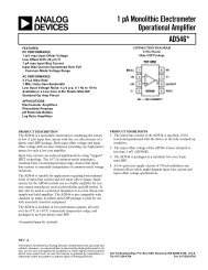
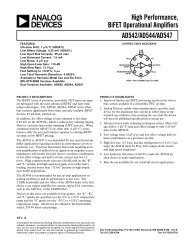
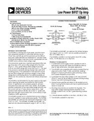
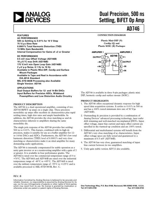
CONNECTION DIAGRAM<br />
Plastic Mini-DIP (N)<br />
Cerdip (Q) and<br />
Plastic SOIC (R) Packages<br />
The <strong>AD746</strong> is available in three 8-pin packages: plastic mini<br />
DIP, hermetic cerdip and surface mount (SOIC).<br />
PRODUCT HIGHLIGHTS<br />
1. The <strong>AD746</strong> offers exceptional dynamic respo<strong>ns</strong>e for high<br />
speed data acquisition systems. It settles to 0.01% in <strong>500</strong> <strong>ns</strong><br />
and has a 100% tested minimum slew rate of 50 V/µs<br />
(<strong>AD746</strong>B).<br />
2. Outstanding dc precision is provided by a combination of<br />
<strong>Analog</strong> <strong>Devices</strong>’ advanced processing technology, laser wafer<br />
drift trimming and well-matched ion-implanted JFETs. Input<br />
offset voltage, input bias current and input offset current are<br />
specified in the warmed-up condition and are 100% tested.<br />
3. Differential and multichannel systems will benefit from the<br />
<strong>AD746</strong>’s very close matching of ac characteristics. Input<br />
offset voltage specs are fully tested and guaranteed to a<br />
maximum of 0.5 mV (<strong>AD746</strong>B).<br />
4. The <strong>AD746</strong> has very close, guaranteed matching of input<br />
bias current between its two amplifiers.<br />
5. Unity gain stable version AD712 also available.<br />
REV. B<br />
Information furnished by <strong>Analog</strong> <strong>Devices</strong> is believed to be accurate and<br />
reliable. However, no respo<strong>ns</strong>ibility is assumed by <strong>Analog</strong> <strong>Devices</strong> for its<br />
use, nor for any infringements of patents or other rights of third parties<br />
which may result from its use. No lice<strong>ns</strong>e is granted by implication or<br />
otherwise under any patent or patent rights of <strong>Analog</strong> <strong>Devices</strong>.<br />
One Technology Way, P.O. Box 9106, Norwood, MA 02062-9106, U.S.A.<br />
Tel: 617/329-4700 Fax: 617/326-8703
<strong>AD746</strong>–SPECIFICATIONS (@ +25C and 15 V dc, unless otherwise noted)<br />
<strong>AD746</strong>J/A <strong>AD746</strong>B <strong>AD746</strong>S<br />
Model Conditio<strong>ns</strong> Min Typ Max Min Typ Max Min Typ Max Units<br />
INPUT OFFSET VOLTAGE 1<br />
Initial Offset 0.3 1.5 0.25 0.5 0.3 1.0 mV<br />
Offset T MIN to T MAX 2.0 0.7 1.5 mV<br />
vs. Temperature 12 20 5 10 12 20 µV/°C<br />
vs. Supply 2 (PSRR) 80 95 84 100 80 95 dB<br />
vs. Supply (PSRR) T MIN to T MAX 80 84 80 dB<br />
Long Term Stability 15 15 15 µV/month<br />
INPUT BIAS CURRENT 3<br />
Either Input V CM = 0 V 110 250 110 150 110 250 pA<br />
Either Input @ T MAX V CM = 0 V 2.5/7 5.7/16 7 9.6 113 256 nA<br />
Either Input V CM = +10 V 145 350 145 200 145 350 pA<br />
Offset Current V CM = 0 V 45 125 45 75 45 125 pA<br />
Offset Current @ T MAX V CM = 0 V 1.0/3 2.8/8 3 4.8 45 128 nA<br />
MATCHING CHARACTERISTICS<br />
Input Offset Voltage 0.6 1.5 0.3 0.5 0.6 1.0 mV<br />
Input Offset Voltage T MIN to T MAX 2.0 0.7 1.5 mV<br />
Input Offset Voltage Drift 20 20 20 µV/°C<br />
Input Bias Current 125 75 125 pA<br />
Crosstalk @ 1 kHz 120 120 120 dB<br />
@ 100 kHz 90 90 90 dB<br />
FREQUENCY RESPONSE<br />
Gain BW, Small Signal G = –1 8 13 9 13 8 13 MHz<br />
Slew Rate, Unity Gain G = –1 45 75 50 75 45 75 V/µs<br />
Full Power Respo<strong>ns</strong>e V O = 20 V p-p 600 600 600 kHz<br />
<strong>Settling</strong> Time to 0.01% 4 G = 1 0.5 0.75 0.5 0.75 0.5 0.75 µs<br />
Total Harmonic<br />
Distortion<br />
f = 1 kHz<br />
R1 ≥ 2 kΩ<br />
V O = 3 V rms 0.0001 0.0001 0.0001 %<br />
INPUT IMPEDANCE<br />
Differential 2.5 × l0 1l 5.5 2.5 × l0 1l 5.5 2.5 × l0 1l 5.5 ΩpF<br />
Common Mode 2.5 × l0 1l 5.5 2.5 × l0 1l 5.5 2.5 × l0 1l 5.5 ΩpF<br />
INPUT VOLTAGE RANGE<br />
Differential 5 ±20 ±20 ±20 V<br />
Common-Mode Voltage +14.5, –11.5 +14.5, –11.5 +14.5, –11.5 V<br />
Over Max <strong>Op</strong>erating Range 6 –11 +13 –11 +13 –11 +13 V<br />
Common-Mode Rejection Ratio V CM = ±10 V 78 88 82 88 78 88 dB<br />
T MIN to T MAX 76 84 80 84 76 84 dB<br />
V CM = ±11 V 72 84 78 84 72 84 dB<br />
T MIN to T MAX 70 80 74 80 70 80 dB<br />
INPUT VOLTAGE NOISE 0.1 to 10 Hz 2 2 2 µV p-p<br />
f = 10 Hz 45 45 45 nV/Hz<br />
f = 100 Hz 22 22 22 nV/Hz<br />
f = 1 kHz 18 18 18 nV/Hz<br />
f = 10 kHz 16 16 16 nV/Hz<br />
INPUT CURRENT NOISE f = 1 kHz 0.01 0.01 0.01 pA/Hz<br />
OPEN LOOP GAIN<br />
V O = ±10 V<br />
R1 ≥ 2 kΩ 150 300 175 300 150 300 V/mV<br />
T MIN to T MAX 75 200 75 200 65 175 V/mV<br />
OUTPUT CHARACTERISTICS<br />
Voltage R1 ≥ 2 kΩ +13, –12.5 +13.9, –13.3 +13, –12.5 +13.9, –13.3 +13, –12.5 +13.9, –13.3 V<br />
T MIN to T MAX ±12 +13.8, –13.1 12 +13.8, –13.1 12 +13.8, –13.1 V<br />
Current Short Circuit 25 25 25 mA<br />
Max Capacitive Load Gain = –1 50 50 50 pF<br />
Driving Capability Gain = –10 <strong>500</strong> <strong>500</strong> <strong>500</strong> pF<br />
POWER SUPPLY<br />
Rated Performance ±15 ±15 ±15 V<br />
<strong>Op</strong>erating Range 4.5 18 4.5 18 4.5 18 V<br />
Quiescent Current 7 10 7 8.0 7 10 mA<br />
TEMPERATURE RANGE<br />
Rated Performance 0 to +70/–40 to +85 –40 to +85 –55 to +125 °C<br />
PACKAGE OPTIONS<br />
8-Pin Plastic Mini-DIP (N-8) <strong>AD746</strong>JN<br />
8-Pin Cerdip (Q-8) <strong>AD746</strong>AQ <strong>AD746</strong>BQ <strong>AD746</strong>SQ<br />
8-Pin Surface Mount (R-8) <strong>AD746</strong>JR<br />
Tape and Reel <strong>AD746</strong>JR-REEL<br />
Chips <strong>AD746</strong>SCHIPS<br />
TRANSISTOR COUNT 54 54 54<br />
–2–<br />
REV. B
<strong>AD746</strong><br />
NOTES<br />
1 Input Offset Voltage specificatio<strong>ns</strong> are guaranteed after 5 minutes of operation at T A = +25°C.<br />
2 PSRR test conditio<strong>ns</strong>: +V S = 15 V, –V S = –12 V to –18 V and +V S = 12 V to 18 V, –V S = –15 V.<br />
3 Bias Current Specificatio<strong>ns</strong> are guaranteed maximum at either input after 5 minutes of operation at T A = +25°C. For higher temperature, the current doubles every<br />
10°C.<br />
4 Gain = –1, Rl = 2 k, Cl = 10 pF.<br />
5 Defined as voltage between inputs, such that neither exceeds ±10 V from ground.<br />
6 Typically exceeding –14.1 V negative common-mode voltage on either input results in an output phase reversal.<br />
Specificatio<strong>ns</strong> subject to change without notice.<br />
Specificatio<strong>ns</strong> in boldface are tested on all production units at final electrical test. Results from those tests are used to calculate outgoing quality levels. All min and<br />
max specificatio<strong>ns</strong> are guaranteed, although only those shown in boldface are tested on all production units.<br />
ABSOLUTE MAXIMUM RATINGS 1<br />
Supply Voltage . . . . . . . . . . . . . . . . . . . . . . . . . . . . . . . . .±18 V<br />
Internal Power Dissipation 2 . . . . . . . . . . . . . . . . . . . . . <strong>500</strong> mW<br />
Input Voltage . . . . . . . . . . . . . . . . . . . . . . . . . . . . . . . . . . .±V S<br />
Output Short Circuit Duration<br />
(For One Amplifier) . . . . . . . . . . . . . . . . . . . . . . . Indefinite<br />
Differential Input Voltage . . . . . . . . . . . . . . . . . . +V S and –V S<br />
Storage Temperature Range (Q) . . . . . . . . . . –65°C to +150°C<br />
Storage Temperature Range (N, R) . . . . . . . . –65°C to +125°C<br />
<strong>Op</strong>erating Temperature Range<br />
<strong>AD746</strong>J . . . . . . . . . . . . . . . . . . . . . . . . . . . . . .0°C to +70°C<br />
<strong>AD746</strong>A/B . . . . . . . . . . . . . . . . . . . . . . . . . . –40°C to +85°C<br />
<strong>AD746</strong>S . . . . . . . . . . . . . . . . . . . . . . . . . . . –55°C to +125°C<br />
Lead Temperature Range<br />
(Soldering 60 seconds) . . . . . . . . . . . . . . . . . . . . . . . +300°C<br />
ESD Rating . . . . . . . . . . . . . . . . . . . . . . . . . . . . . . . . . . . . . . .<br />
NOTES<br />
1 Stresses above those listed under “Absolute Maximum Ratings” may cause<br />
permanent damage to the device. This is a stress rating only and functional<br />
operation of the device at these or any other conditio<strong>ns</strong> above those indicated in<br />
the operational section of this specification is not implied. Exposure to absolute<br />
maximum rating conditio<strong>ns</strong> for extended periods may affect device reliability.<br />
2 8-Pin Plastic Package: θ JA = 100°C/Watt, θ JC = 50°C/Watt<br />
8-Pin Cerdip Package: θ JA = 110°C/Watt, θ JC = 30°C/Watt<br />
8-Pin Small Outline Package: θ JA = 160°C/Watt, θ JC = 42°C/Watt<br />
METALIZATION PHOTOGRAPH<br />
Contact factory for latest dime<strong>ns</strong>io<strong>ns</strong>.<br />
Dime<strong>ns</strong>io<strong>ns</strong> shown in inches and (mm).<br />
CAUTION<br />
ESD (electrostatic discharge) se<strong>ns</strong>itive device. Electrostatic charges as high as 4000 V readily<br />
accumulate on the human body and test equipment and can discharge without detection.<br />
Although the <strong>AD746</strong> features proprietary ESD protection circuitry, permanent damage may<br />
occur on devices subjected to high energy electrostatic discharges. Therefore, proper ESD<br />
precautio<strong>ns</strong> are recommended to avoid performance degradation or loss of functionality.<br />
WARNING!<br />
ESD SENSITIVE DEVICE<br />
REV. B –3–
<strong>AD746</strong>–Typical Characteristics<br />
Figure 1. Input Voltage Swing vs.<br />
Supply Voltage<br />
Figure 2. Output Voltage Swing<br />
vs. Supply Voltage<br />
Figure 3. Output Voltage Swing<br />
vs. Load Resistance<br />
.<br />
Figure 4. Quiescent Current vs.<br />
Supply Voltage<br />
Figure 5. Input Bias Current vs.<br />
Temperature<br />
Figure 6. Output Impedance vs.<br />
Frequency<br />
Figure 7. Input Bias Current vs.<br />
Common Mode Voltage<br />
Figure 8. Short Circuit Current<br />
Limit vs. Temperature<br />
Figure 9. Gain Bandwidth Product<br />
vs. Temperature<br />
–4– REV. B
<strong>AD746</strong><br />
Figure 10. <strong>Op</strong>en Loop Gain and<br />
Phase Margin vs. Frequency<br />
Figure 11. <strong>Settling</strong> Time vs.<br />
Closed Loop Voltage Gain<br />
Figure 12. <strong>Op</strong>en Loop Gain vs.<br />
Supply Voltage<br />
Figure 13. Common-Mode and<br />
Power Supply Rejection vs.<br />
Frequency<br />
Figure 14. Large Signal Frequency<br />
Respo<strong>ns</strong>e<br />
Figure 15. Output Swing and<br />
Error vs. <strong>Settling</strong> Time<br />
Figure 16. Total Harmonic<br />
Distortion vs. Frequency Using<br />
Circuit of Figure 19<br />
Figure 17. Input Noise Voltage<br />
Spectral De<strong>ns</strong>ity<br />
Figure 18. Slew Rate vs. Input<br />
Error Signal<br />
REV. B –5–
<strong>AD746</strong><br />
POWER SUPPLY BYPASSING<br />
The power supply connectio<strong>ns</strong> to the <strong>AD746</strong> must maintain a<br />
low impedance to ground over a bandwidth of 13 MHz or more.<br />
This is especially important when driving a significant resistive<br />
or capacitive load, since all current delivered to the load comes<br />
from the power supplies. Multiple high quality bypass capacitors<br />
are recommended for each power supply line in any critical<br />
application. A 0.1 µF ceramic and a 1 µF tantalum capacitor as<br />
shown in Figure 20 placed as close as possible to the amplifier<br />
(with short lead lengths to power supply common) will assure<br />
adequate high frequency bypassing, in most applicatio<strong>ns</strong>. A<br />
minimum bypass capacitance of 0.1 µF should be used for any<br />
application.<br />
If only one of the two amplifiers i<strong>ns</strong>ide the <strong>AD746</strong> is to be<br />
utilized, the unused amplifier should be connected as shown in<br />
Figure 21a. Note that the noninverting input should be<br />
grounded and that R L and C L are not required.<br />
Figure 19. THD Test Circuit<br />
Figure 20. Power Supply<br />
Bypassing<br />
Figure 21a. Gain of 2 Follower<br />
Figure 21b. Gain of 2 Follower<br />
Large Signal Pulse Respo<strong>ns</strong>e<br />
Figure 21c. Gain of 2 Follower<br />
Small Signal Pulse Respo<strong>ns</strong>e<br />
Figure 22a. Unity Gain Inverter<br />
Figure 22b. Unity Gain Inverter<br />
Large Signal Pulse Respo<strong>ns</strong>e<br />
Figure 22c. Unity Gain Inverter<br />
Small Signal Pulse Respo<strong>ns</strong>e<br />
–6– REV. B
<strong>AD746</strong><br />
A HIGH SPEED 3 OR AMP INSTRUMENTATION<br />
AMPLIFIER CIRCUIT<br />
The i<strong>ns</strong>trumentation amplifier circuit shown in Figure 23 can<br />
provide a range of gai<strong>ns</strong> from 2 up to 1000 and higher. The<br />
circuit bandwidth is 2.5 MHz at a gain of 2 and 750 kHz at a<br />
gain of 10; settling time for the entire circuit is less than 2 µs to<br />
within 0.01% for a 10 volt step, (G = 10).<br />
Table I. Performance Summary for the 3 <strong>Op</strong> Amp<br />
I<strong>ns</strong>trumentation Amplifier Circuit<br />
T SETTLE<br />
Gain R G Bandwidth (0.01%)<br />
2 20 kΩ 2.5 MHz 1.0 µs<br />
10 4.04 kΩ 1 MHz 2.0 µs<br />
100 404 Ω 290 kHz 5.0 µs<br />
Figure 23. A High Performance, 3 <strong>Op</strong> Amp, I<strong>ns</strong>trumentation<br />
Amplifier Circuit<br />
Figure 25. <strong>Settling</strong> Time of the 3 <strong>Op</strong><br />
Amp I<strong>ns</strong>trumentation Amplifier.<br />
Gain = 10, Horizontal Scale: 0.5 µs/Div,<br />
Vertical Scale: 5 V/Div.<br />
Error Signal Scale: 0.01%/Div.<br />
THD Performance Co<strong>ns</strong>ideratio<strong>ns</strong><br />
The <strong>AD746</strong> was carefully optimized to offer excellent<br />
performance in terms of total harmonic distortion (THD) in<br />
signal processing applicatio<strong>ns</strong>. The THD level when operating<br />
the <strong>AD746</strong> in inverting gain applicatio<strong>ns</strong> will show a gradual<br />
rise from the distortion floor of 20 dB/decade (see Figure 28).<br />
In noninverting applicatio<strong>ns</strong>, care should be taken to balance<br />
the source impedances at both the inverting and noninverting<br />
inputs, to avoid distortion caused by the modulation of input<br />
capacitance inherent in all <strong>BiFET</strong> op amps.<br />
Figure 26. THD Measurement, Inverter Circuit<br />
Figure 24. Pulse Respo<strong>ns</strong>e of the 3<br />
<strong>Op</strong> Amp I<strong>ns</strong>trumentation Amplifier.<br />
Gain = 10, Horizontal Scale:<br />
0.5 µs/Div, Vertical Scale: 5 V/Div.<br />
Figure 27. THD Measurement, Follower Circuit<br />
REV. B –7–
<strong>AD746</strong><br />
OUTLINE DIMENSIONS<br />
Dime<strong>ns</strong>io<strong>ns</strong> shown in inches and (mm).<br />
Mini-DIP (N) Package<br />
C1319–10–9/89<br />
Figure 28. THD vs. Frequency Using Standard Distortion<br />
Analyzer<br />
2kΩ<br />
Cerdip (Q) Package<br />
SINE WAVE<br />
GENERATOR<br />
20V p-p<br />
OUTPUT<br />
LEVEL<br />
2kΩ<br />
2 –<br />
1/2<br />
<strong>AD746</strong><br />
3 + 4<br />
–V S<br />
1µF + 0.1µF<br />
1<br />
V OUT<br />
#1<br />
20V p-p<br />
20kΩ<br />
2.21kΩ<br />
+V S<br />
1µF + 0.1µF<br />
6 –<br />
1/2 8<br />
<strong>AD746</strong> 7<br />
5 +<br />
V OUT<br />
#2<br />
V<br />
CROSSTALK = 20 OUT #1<br />
LOG10<br />
V OUT #2 + 20dB<br />
Figure 29. Crosstalk Test Circuit<br />
Plastic Small Outline<br />
(R) Package<br />
Figure 30. Crosstalk vs. Frequency<br />
PRINTED IN U.S.A.<br />
–8– REV. B