Intel(r) 82552V Fast Ethernet PHY Datasheet
Intel(r) 82552V Fast Ethernet PHY Datasheet
Intel(r) 82552V Fast Ethernet PHY Datasheet

Create successful ePaper yourself
Turn your PDF publications into a flip-book with our unique Google optimized e-Paper software.
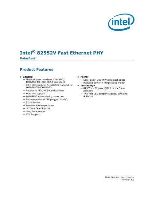
<strong>Intel</strong> ® <strong>82552V</strong> <strong>Fast</strong> <strong>Ethernet</strong> <strong>PHY</strong><br />
<strong>Datasheet</strong><br />
Product Features<br />
• General<br />
— Physical layer interface 10BASE-T/<br />
100BASE-TX IEEE 802.3 compliant.<br />
— IEEE 802.3u Auto-Negotiation support for<br />
10BASE-T/100BASE-TX<br />
— Automatic MDI/MDI-X switch-over<br />
— XOR tree support<br />
— 10BASE-T auto-polarity correction<br />
— Auto-detection of "Unplugged mode".<br />
—3.3 V device<br />
— Reverse auto negotiation .<br />
— LCI Interface Support<br />
— Loop back support<br />
— PXE Support<br />
• Power<br />
— Low Power: 310 mW at fastest speed<br />
— Reduced power in "Unplugged mode"<br />
• Technology<br />
— <strong>82552V</strong> - 32 pins, QfN 5 mm x 5 mm<br />
package<br />
— Two Port LED support (Speed, Link and<br />
Activity)<br />
Order Number: 322322-001EN<br />
Revision 1.9
Legal Lines and Disclaimers<br />
INFORMATION IN THIS DOCUMENT IS PROVIDED IN CONNECTION WITH INTEL® PRODUCTS. NO LICENSE, EXPRESS OR IMPLIED, BY ESTOPPEL OR<br />
OTHERWISE, TO ANY INTELLECTUAL PROPERTY RIGHTS IS GRANTED BY THIS DOCUMENT. EXCEPT AS PROVIDED IN INTEL'S TERMS AND CONDITIONS<br />
OF SALE FOR SUCH PRODUCTS, INTEL ASSUMES NO LIABILITY WHATSOEVER, AND INTEL DISCLAIMS ANY EXPRESS OR IMPLIED WARRANTY, RELATING<br />
TO SALE AND/OR USE OF INTEL PRODUCTS INCLUDING LIABILITY OR WARRANTIES RELATING TO FITNESS FOR A PARTICULAR PURPOSE,<br />
MERCHANTABILITY, OR INFRINGEMENT OF ANY PATENT, COPYRIGHT OR OTHER INTELLECTUAL PROPERTY RIGHT. <strong>Intel</strong> products are not intended for<br />
use in medical, life saving, life sustaining, critical control or safety systems, or in nuclear facility applications.<br />
<strong>Intel</strong> may make changes to specifications and product descriptions at any time, without notice.<br />
<strong>Intel</strong> Corporation may have patents or pending patent applications, trademarks, copyrights, or other intellectual property rights that relate to the<br />
presented subject matter. The furnishing of documents and other materials and information does not provide any license, express or implied, by estoppel<br />
or otherwise, to any such patents, trademarks, copyrights, or other intellectual property rights.<br />
IMPORTANT - PLEASE READ BEFORE INSTALLING OR USING INTEL® PRE-RELEASE PRODUCTS.<br />
Please review the terms at http://www.intel.com/netcomms/prerelease_terms.htm carefully before using any <strong>Intel</strong>® pre-release product, including any<br />
evaluation, development or reference hardware and/or software product (collectively, “Pre-Release Product”). By using the Pre-Release Product, you<br />
indicate your acceptance of these terms, which constitute the agreement (the “Agreement”) between you and <strong>Intel</strong> Corporation (“<strong>Intel</strong>”). In the event<br />
that you do not agree with any of these terms and conditions, do not use or install the Pre-Release Product and promptly return it unused to <strong>Intel</strong>.<br />
Designers must not rely on the absence or characteristics of any features or instructions marked “reserved” or “undefined.” <strong>Intel</strong> reserves these for<br />
future definition and shall have no responsibility whatsoever for conflicts or incompatibilities arising from future changes to them.<br />
<strong>Intel</strong> processor numbers are not a measure of performance. Processor numbers differentiate features within each processor family, not across different<br />
processor families. See http://www.intel.com/products/processor_number for details.<br />
This document contains information on products in the design phase of development. The information here is subject to change without notice. Do not<br />
finalize a design with this information.<br />
The <strong>82552V</strong> GbE <strong>PHY</strong> may contain design defects or errors known as errata which may cause the product to deviate from published specifications.<br />
Current characterized errata are available on request.<br />
Hyper-Threading Technology requires a computer system with an <strong>Intel</strong> ® Pentium ® 4 processor supporting HT Technology and a HT Technology enabled<br />
chipset, BIOS and operating system. Performance will vary depending on the specific hardware and software you use. See http://www.intel.com/<br />
products/ht/Hyperthreading_more.htm for additional information.<br />
Contact your local <strong>Intel</strong> sales office or your distributor to obtain the latest specifications and before placing your product order.<br />
Copies of documents which have an ordering number and are referenced in this document, or other <strong>Intel</strong> literature, may be obtained from:<br />
<strong>Intel</strong> Corporation<br />
P.O. Box 5937<br />
Denver, CO 80217-9808<br />
or call in North America 1-800-548-4725, Europe 44-0-1793-431-155, France 44-0-1793-421-777, Germany 44-0-1793-421-333, other Countries 708-<br />
296-9333.<br />
<strong>Intel</strong> and <strong>Intel</strong> logo are trademarks or registered trademarks of <strong>Intel</strong> Corporation or its subsidiaries in the United States and other countries.<br />
*Other names and brands may be claimed as the property of others.<br />
Copyright © 2008-2009, <strong>Intel</strong> Corporation. All Rights Reserved.<br />
ii
<strong>Datasheet</strong>—<strong>82552V</strong> <strong>Fast</strong> <strong>Ethernet</strong> <strong>PHY</strong><br />
Contents<br />
1.0 Introduction ..............................................................................................................1<br />
1.1 Scope ................................................................................................................1<br />
1.2 Overview ...........................................................................................................1<br />
1.3 References .........................................................................................................2<br />
1.4 Product Codes.....................................................................................................2<br />
2.0 Interconnects............................................................................................................3<br />
2.1 Introduction .......................................................................................................3<br />
2.2 JCLK Clock .........................................................................................................3<br />
2.3 JRSTSYNC ..........................................................................................................3<br />
2.4 XOR Test Interface ..............................................................................................3<br />
3.0 Pin Interface .............................................................................................................5<br />
3.1 Pin Assignment ...................................................................................................5<br />
3.1.1 Signal Type Definitions..............................................................................5<br />
3.2 Pin Descriptions ..................................................................................................6<br />
4.0 Package.....................................................................................................................7<br />
4.1 Package Type and Epad Size.................................................................................7<br />
4.2 Package Electrical and Thermal Characteristics ........................................................8<br />
4.3 Power and Ground Requirements...........................................................................8<br />
4.3.1 Power Delivery.........................................................................................8<br />
4.4 Pinouts (Top View, Pins Down) ............................................................................ 10<br />
5.0 Initialization............................................................................................................ 13<br />
5.1 Power Up Sequence ........................................................................................... 13<br />
5.2 Reset Operation ................................................................................................ 14<br />
6.0 Power Management and Delivery............................................................................. 15<br />
6.1 Power Consumption........................................................................................... 15<br />
6.2 Power Saving Feature ........................................................................................ 15<br />
6.2.1 Low-Power Link Up (LPLU)....................................................................... 15<br />
7.0 Electrical and Timing Specifications......................................................................... 17<br />
7.1 Introduction ..................................................................................................... 17<br />
7.2 Operating Conditions ......................................................................................... 17<br />
7.2.1 Absolute Maximum Operating Conditions ................................................... 17<br />
7.2.2 3.3 V Rail Requirements .......................................................................... 17<br />
7.2.3 DC Characteristics .................................................................................. 18<br />
7.2.4 3.3 V I/O Interfaces DC Characteristics ..................................................... 18<br />
7.2.5 LED DC Characteristics............................................................................ 19<br />
7.2.6 AC Characteristics .................................................................................. 19<br />
7.2.7 Reset (JRSTSYNC) Timing Parameters ....................................................... 22<br />
7.2.8 Crystal Information ................................................................................ 22<br />
7.2.9 Crystal Specifications.............................................................................. 22<br />
7.3 Discrete/Integrated Magnetics Specification .......................................................... 23<br />
8.0 Programmers’ Visible State ..................................................................................... 25<br />
8.1 Extended Register description ............................................................................. 44<br />
9.0 Non-Volatile Memory (NVM) .................................................................................... 51<br />
9.1 Introduction ..................................................................................................... 51<br />
9.2 EEUPDATE Utility............................................................................................... 51<br />
9.2.1 Command Line Parameters ...................................................................... 51<br />
10.0 Checklists ................................................................................................................ 53<br />
iii
<strong>82552V</strong> <strong>Fast</strong> <strong>Ethernet</strong> <strong>PHY</strong>—<strong>Datasheet</strong><br />
11.0 Reference Schematics ..............................................................................................55<br />
12.0 Models .....................................................................................................................59<br />
iv
<strong>Datasheet</strong>—<strong>82552V</strong> <strong>Fast</strong> <strong>Ethernet</strong> <strong>PHY</strong><br />
Revision History<br />
Date Revision Description<br />
September 2008 0.5 Initial public release.<br />
February 2009 0.75<br />
Added power delivery diagram. Added reset effects table. Updated Reference Documents<br />
list. Removed preliminary oscillator information. Added magnetics specifications.<br />
Corrected pinout diagram and pin description table. Updated power consumption table.<br />
April 2009 1.0 Corrected pinout diagram and pin description table. Updated power consumption table.<br />
May 2009 1.1<br />
Updated power value. Updated RBIAS value. Removed chipset reference and added<br />
platform chipset name, Tiger Point. Updated Signal Definition table. Updated mechanical<br />
drawing and assembly information. Updated Low-Power Link Up section. Corrected signal<br />
name in Figure 8.<br />
July 2009 1.9 Updated measured power table; removed <strong>Intel</strong> Confidential designation.<br />
v
<strong>82552V</strong> <strong>Fast</strong> <strong>Ethernet</strong> <strong>PHY</strong>—<strong>Datasheet</strong><br />
1.0 Introduction<br />
1.1 Scope<br />
This document describes the external architecture for the <strong>82552V</strong>. It's intended to be a<br />
reference for software developers of device drivers, board designers, test engineers, or<br />
anyone else who might need specific technical or programming information about the<br />
<strong>82552V</strong>.<br />
1.2 Overview<br />
The <strong>Intel</strong> ® <strong>82552V</strong> 10/100 Mbps Platform LAN Connect is a highly-integrated device<br />
designed for 10 or 100 Mbps <strong>Ethernet</strong> systems. It is based on the IEEE 10BASE-T and<br />
100BASE-TX standards.<br />
The IEEE 802.3u standard for 100BASE-TX defines networking over two pairs of<br />
Category 5 unshielded twisted pair cable or Type 1 shielded twisted pair cable.<br />
The <strong>82552V</strong> conforms with the IEEE 802.3u Auto-Negotiation standard and the IEEE<br />
802.3x Full Duplex Flow Control standard. The <strong>82552V</strong> also includes a <strong>PHY</strong> interface<br />
compliant to the current platform LAN connect interface.<br />
The <strong>82552V</strong> only operates with the ITiger Point chipset that incorporates the MAC. An<br />
interface for a Platform Controller Hub (PCH) is also available--contact your <strong>Intel</strong><br />
representative for more information.<br />
The <strong>82552V</strong> is packaged in a small footprint QFN package with 32 pins, 5 mm x 5 mm<br />
with 0.5 mm pitch, making it very useful for small form-factor platforms.<br />
The <strong>82552V</strong> interfaces with its MAC through the LCI-based interface.<br />
LCI<br />
LCI<br />
Crystal<br />
PLL<br />
Testability<br />
MII<br />
MDIO<br />
Status & Control<br />
Power<br />
Power<br />
Supply<br />
<strong>PHY</strong><br />
LEDs<br />
<strong>82552V</strong><br />
MDI<br />
Figure 1.<br />
<strong>82552V</strong> Block Diagram<br />
1
<strong>Datasheet</strong>—<strong>82552V</strong> <strong>Fast</strong> <strong>Ethernet</strong> <strong>PHY</strong><br />
1.3 References<br />
• IEEE 802.3 Standard for Local and Metropolitan Area Networks, Institute of<br />
Electrical and Electronics Engineers.<br />
• • LAN Connect Interface Specification. <strong>Intel</strong> Corporation.<br />
• • I/O Control Hub 2, 3, and 4 EEPROM Map and Programming Information. <strong>Intel</strong><br />
Corporation.<br />
• • I/O Control Hub 5, 6, and 7 EEPROM Map and Programming Information. <strong>Intel</strong><br />
Corporation<br />
Programming information can be obtained through your local <strong>Intel</strong> representatives.<br />
1.4 Product Codes<br />
Table 1 lists the product ordering codes for the <strong>82552V</strong> <strong>Ethernet</strong> controller.<br />
Table 1.<br />
Product Ordering Code<br />
Device<br />
<strong>82552V</strong><br />
Product Code<br />
WG<strong>82552V</strong><br />
§ §<br />
2
<strong>82552V</strong> <strong>Fast</strong> <strong>Ethernet</strong> <strong>PHY</strong>—<strong>Datasheet</strong><br />
2.0 Interconnects<br />
2.1 Introduction<br />
The <strong>82552V</strong> implements the LCI interconnect to the MAC:<br />
It is an eight-pin interface that incorporates all MII management functionality. The<br />
interface includes reset functionality as well.<br />
2.2 JCLK Clock<br />
The <strong>82552V</strong> drives a 50 Mhz clock or a 5 Mhz clock to the MAC depending on the<br />
selected technology: 100base-TX or 10Base-T respectively. The <strong>82552V</strong> does not stop<br />
the LCI clock in any case. During reduced power mode, the <strong>82552V</strong> drives a 5 Mhz<br />
clock.<br />
2.3 JRSTSYNC<br />
The <strong>82552V</strong> filters out any JRSTSYNC pulses with width less than 200 ns to distinguish<br />
between a RESET and a SYNC pulse. For resetting the <strong>82552V</strong>, the reset should be<br />
longer than 500 us.<br />
2.4 XOR Test Interface<br />
Signal<br />
LED_10_100n<br />
LED_ACTn<br />
JRXD0<br />
JRXD1<br />
JRXD2<br />
JTXD0<br />
JTXD1<br />
JTXD2<br />
JCLK<br />
JRSTSYNC<br />
RSVD _IN_1<br />
RSVD _IN_32<br />
Type<br />
XOR output<br />
XOR input<br />
XOR input<br />
XOR input<br />
XOR input<br />
XOR input<br />
XOR input<br />
XOR input<br />
XOR input<br />
XOR input<br />
XOR input<br />
XOR input<br />
3
<strong>Datasheet</strong>—<strong>82552V</strong> <strong>Fast</strong> <strong>Ethernet</strong> <strong>PHY</strong><br />
Note:<br />
This page intentionally left blank.<br />
4
<strong>82552V</strong> <strong>Fast</strong> <strong>Ethernet</strong> <strong>PHY</strong>—<strong>Datasheet</strong><br />
3.0 Pin Interface<br />
3.1 Pin Assignment<br />
The <strong>82552V</strong> is packaged in a 32-pin package, 5 x 5 mm with a 0.5 mm lead pitch.<br />
There are 32 pins on the periphery and a die pad (Exposed Pad*) for ground.<br />
3.1.1 Signal Type Definitions<br />
Signal Type<br />
I<br />
O<br />
T/s<br />
S/t/s<br />
O/d<br />
Analog<br />
AI<br />
AO<br />
B<br />
P<br />
PD<br />
PU<br />
IH<br />
Definition<br />
A standard input-only signal.<br />
Totem pole output is a standard active driver.<br />
Tri-state is a bi-directional, tri-state input/output pin.<br />
Sustained tri-state is an active low tri-state signal owned and driven by one and only one<br />
agent at a time. The agent that drives an s/t/s pin low must drive it high for at least one<br />
clock before letting it float. A new agent cannot start driving an s/t/s signal any sooner than<br />
one clock after the previous owner tri-states it.<br />
Open drain enables multiple devices to share as a wire-OR.<br />
Analog input/output signal.<br />
Analog input signal.<br />
Analog output signal.<br />
Input bias<br />
Power<br />
Pull down<br />
Pull up<br />
Digital input with hysteresis<br />
5
<strong>Datasheet</strong>—<strong>82552V</strong> <strong>Fast</strong> <strong>Ethernet</strong> <strong>PHY</strong><br />
3.2 Pin Descriptions<br />
Pin Name Pin # Pin type Description<br />
VDD2P5_OUT 1 AO<br />
2.5V regulator output. A 1uF plus several 0.1uF cap needed to<br />
stabilize the output. It is for analog, digital I/O and the<br />
transformer center taps<br />
VDD3P3_IN 2 P 3.3 V<br />
DVDD1P2_3 3 P Digital 1.2V<br />
RSVD_IN_4 4 I, PU (low voltage)<br />
Select either 25 MHz or 48 MHz external clock source. Float=25<br />
MHz, GND=48 MHz<br />
XTAL_OUT 5 AO<br />
Crystal oscillator output. 27pF to GND. An external clock source<br />
with 0-1.2V swing can inject to this pin when crystal is not used<br />
XTAL_IN 6 AI Crystal oscillator input, 27pF to GND.<br />
VDD1P2_OUT 7 P<br />
1.2V regulator output. Two 0.1uF caps or one 1uF cap needed to<br />
stabilize the output.<br />
RBIAS 8 AO Connect 2.26 kOhm +1% to GND<br />
MDI_PLUS0/<br />
MDI_MINUS0<br />
MDI_PLUS1/<br />
MDI_MINUS1<br />
9, 10 AI, AO<br />
11, 12 AI, AO<br />
Media Dependent interface 0, terminated with two 49.9 resistors<br />
and connect to XFMR<br />
Media Dependent interface 1, terminated with two 49.9 resistors<br />
and connect to XFMR<br />
AVDD2P5_13 13 P Analog 2.5 V<br />
RSVD _IN_14 14 I/O, PU Reserved input pin. Tie to 3.3V through a 10 kOhm resistor.<br />
RSVD _IN_15 15 I/O, PU Reserved input pin. Tie to 3.3V through a 10 kOhm resistor<br />
TEST_EN 16 I, PD Test enable.<br />
LED_10_100# 17<br />
I/O, PU,<br />
input is only for test<br />
Parallel LED output for 10/100BASE-T, 0 = 100 BT<br />
1 = 10 BT<br />
LED_ACT# 18<br />
I/O, PU,<br />
input is only for test<br />
Parallel LED activity indicator, active low<br />
JTAG_TDI 19 I/O, PU, Jtag data in<br />
JTAG_TMS 20 I/O, PU, Jtag tms<br />
JTAG_TDO 21 I/O, PU, Jtag data out<br />
JTAG_TCK 22 I/O, PU, Jtag clk<br />
DVDD2P5_23 23 P Digital I/O 2.5V<br />
JRXD2 24<br />
I/O, PU,<br />
input is only for test<br />
50 Mbps receive out<br />
JRXD1 25<br />
I/O, PU,<br />
input is only for test<br />
50 Mbps receive out<br />
JRXD0 26<br />
I/O, PU,<br />
input is only for test<br />
50 MHz receive out<br />
JCLK 27<br />
I/O, PU,<br />
input is only for test<br />
Clock out<br />
JTXD2 28 I, PU, Transmit input<br />
JTXD1 29 I, PU, Transmit input<br />
JTXD0 30 I, PU, Transmit input<br />
JRSTSYNC 31 IH, PU, System reset input<br />
RSVD _IN_32 32 IH, PU, Reserved input pin. Tie to 3.3 V through a 10 kOhm resistor<br />
6
<strong>82552V</strong> <strong>Fast</strong> <strong>Ethernet</strong> <strong>PHY</strong>—<strong>Datasheet</strong><br />
4.0 Package<br />
4.1 Package Type and Epad Size<br />
The <strong>82552V</strong> is a 5 mm x 5 mm, 32-pin QFN package with a pad size of 2.7 mm x 2.7<br />
mm.<br />
Symbol<br />
Package Dimensions<br />
MIN NOM MAX<br />
Note<br />
e<br />
0.50 BSC<br />
N<br />
32<br />
3<br />
Nd<br />
8<br />
3<br />
Ne<br />
8<br />
3<br />
L 0.30 0.40 0.50<br />
b 0.18 0.23 0.30 4<br />
Q - - -<br />
D2 See Exposed Pad Dimensions<br />
E2 See Exposed Pad Dimensions<br />
Exposed Pad<br />
SYMBOL<br />
EXPOSED PAD<br />
Symbol<br />
A<br />
A1<br />
A2<br />
A3<br />
D<br />
D1<br />
E<br />
E1<br />
0<br />
_<br />
P<br />
O<br />
R<br />
D2 E2 NOTE<br />
MIN NOM MAX MIN NOM MAX<br />
2.60 2.70 2.80 2.60 2.70 2.80<br />
Common Dimensions<br />
Note<br />
MIN NOM MAX<br />
0.80 0.85 0.90<br />
0.00 0.01 0.05 10<br />
0.60 0.65 0.70<br />
0.20 REF<br />
500 BSC<br />
4.75 BSC<br />
5.00 BSC<br />
4.75 BSC<br />
0<br />
_<br />
12’<br />
0.24 0.42 0.60<br />
0.30 0.40 0.65 8,11<br />
0.13 0.17 0.23 8,11<br />
Tolerance Requirement for D1/E1: +/- 0.1 mm<br />
7
<strong>Datasheet</strong>—<strong>82552V</strong> <strong>Fast</strong> <strong>Ethernet</strong> <strong>PHY</strong><br />
4.2 Package Electrical and Thermal Characteristics<br />
Max temperature junction is 120 degrees C.<br />
Velocity (m/s) Theta Ja (c/w) Theta Jb (c/w) Theta Jc (c/w) Psi jt (c/w) Psi jb (c/w)<br />
0 52.5 33 11.2 0.9 31.7<br />
1 45.9 33 11.2 1.4 31.3<br />
2.5 41.1 33 11.2 1.9 30.9<br />
No heat sink is required.<br />
4.3 Power and Ground Requirements<br />
The <strong>82552V</strong> requires one power supply.<br />
Note:<br />
Power delivery can be customized based on a specific OEM platform configuration.<br />
4.3.1 Power Delivery<br />
The <strong>82552V</strong> operates from a 3.3 V DC external power rail and internally generates the<br />
2.5 V and 1.2 V supplies.<br />
8
<strong>82552V</strong> <strong>Fast</strong> <strong>Ethernet</strong> <strong>PHY</strong>—<strong>Datasheet</strong><br />
<strong>82552V</strong><br />
+3.3 V LAN<br />
VDD3P3_IN<br />
2<br />
VDD2P5_OUT<br />
1<br />
C13<br />
1 uF<br />
C9<br />
0.1 uF<br />
C10<br />
0.1 uF<br />
To Magnetics<br />
DVDD2P5_23<br />
23<br />
AVDD2P5_13<br />
13<br />
VDD1P2_OUT<br />
7<br />
C1<br />
1 uF<br />
C15<br />
0.1 uF<br />
DVDD1P2_3<br />
3<br />
VSS_EPAD<br />
33<br />
Figure 2.<br />
<strong>82552V</strong> Power Delivery Diagram<br />
9
<strong>Datasheet</strong>—<strong>82552V</strong> <strong>Fast</strong> <strong>Ethernet</strong> <strong>PHY</strong><br />
4.4 Pinouts (Top View, Pins Down)<br />
32 31 30 29 28 27 26 25<br />
G ND on EPAD<br />
VDD 2 P 5 _<br />
O U T<br />
1<br />
JRXD 2<br />
VDD 3P 3 _ IN<br />
2<br />
DVDD2P5_23<br />
DVDD 1P2_3<br />
3<br />
JTAG<br />
_ TCK<br />
RSVD_IN_4<br />
XTAL _ OUT<br />
XTAL _ I N<br />
4<br />
5<br />
6<br />
10/100<br />
<strong>82552V</strong><br />
JTAG _ TDO<br />
JTA G _ TM S<br />
JTAG _ TD I<br />
VDD 1 P 2 _<br />
O U T<br />
7<br />
LED _ ACT #<br />
RBIAS<br />
8<br />
LED _ 10 _ 100 #<br />
9 10 11 12 13 14 15 16<br />
RS V D _ I<br />
N _ 1 4<br />
R S V<br />
D _ I<br />
N _ 1 5<br />
N C<br />
Pin 1<br />
RS V D _ I<br />
J R S T S Y<br />
J T X D 0<br />
J T X D 1<br />
J T X D 2<br />
JCLK<br />
J R X D 0<br />
J R X D 1<br />
24<br />
23<br />
22<br />
QFN<br />
32 Pin + EPad<br />
5 m m x 5 m m<br />
0.5 m m pitch<br />
21<br />
20<br />
19<br />
18<br />
17<br />
M D I_PLUS0<br />
M D I_MIMUS0<br />
M D I_PLUS1<br />
M D I_MINUS1<br />
AVDD2P5_13<br />
T E S T _ E N<br />
N _ 3 2<br />
Figure 3.<br />
<strong>82552V</strong> Pinouts<br />
10
<strong>82552V</strong> <strong>Fast</strong> <strong>Ethernet</strong> <strong>PHY</strong>—<strong>Datasheet</strong><br />
Note:<br />
This page intentionally left blank.<br />
§ §<br />
11
<strong>Datasheet</strong>—<strong>82552V</strong> <strong>Fast</strong> <strong>Ethernet</strong> <strong>PHY</strong><br />
12
<strong>82552V</strong> <strong>Fast</strong> <strong>Ethernet</strong> <strong>PHY</strong>—<strong>Datasheet</strong><br />
5.0 Initialization<br />
5.1 Power Up Sequence<br />
The <strong>82552V</strong> uses a 3.3 V power rail. The rail must meet the LCI power ramp<br />
requirements. The following flowchart shows the power up sequence for the <strong>82552V</strong>.<br />
Power up<br />
Internal power on circuit has<br />
detected valid power on input<br />
pins (3.3/1.0 volts)<br />
Internal Xosc stablizes<br />
Strapping are sampled<br />
Internal Power On Reset is deasserted<br />
<strong>82552V</strong> drives JRXD pins to ‘0’<br />
MAC activates JRSTSYNC<br />
reset<br />
<strong>82552V</strong> detects JRSTSYNC<br />
deassertion<br />
<strong>82552V</strong> drives a 5MHz<br />
clock on JCLK<br />
LCI interface initializes and<br />
becomes active<br />
<strong>PHY</strong> completes internal reset<br />
after JRSTSYNC deassertion<br />
and starts link auto-negotiation<br />
<strong>82552V</strong> MDIO registers are<br />
initialized by the MAC<br />
<strong>PHY</strong> establishes link<br />
Figure 4.<br />
Power Up Sequence Flowchart<br />
13
<strong>Datasheet</strong>—<strong>82552V</strong> <strong>Fast</strong> <strong>Ethernet</strong> <strong>PHY</strong><br />
5.2 Reset Operation<br />
Three resets are available:<br />
• Internal Power On Reset (POR)--the <strong>82552V</strong> has an internal mechanism for sensing<br />
the power pins. Until power is up and stable, the <strong>82552V</strong> generates an internal<br />
active low reset. This reset acts as a master reset for the device.<br />
Strapping values are latched after Internal POR is de-asserted.<br />
• LCI Reset--Reset from JRSTSYNC pin causing complete reset of the <strong>82552V</strong>,<br />
including the <strong>PHY</strong>.<br />
• <strong>PHY</strong> Soft Reset--A <strong>PHY</strong> reset caused by writing to bit 15 in MDIO register 0.<br />
Setting the bit resets the <strong>PHY</strong>, but does not reset non-<strong>PHY</strong> parts.<br />
The effect/impact of these various reset options on these and other registers is listed in<br />
the following table. A (√) indicates that these areas are affected.<br />
Effects/Sources<br />
<strong>PHY</strong> Registers<br />
and States<br />
Strapping<br />
Options<br />
Internal POR √ √<br />
LCI Reset<br />
<strong>PHY</strong> Soft Reset<br />
√<br />
√<br />
14
<strong>82552V</strong> <strong>Fast</strong> <strong>Ethernet</strong> <strong>PHY</strong>—<strong>Datasheet</strong><br />
6.0 Power Management and Delivery<br />
This section describes how power management is implemented in the <strong>82552V</strong>.<br />
6.1 Power Consumption<br />
The following table lists the measured power:<br />
Table 2.<br />
Measured Power<br />
Mode<br />
Description<br />
<strong>Intel</strong>® <strong>82552V</strong> <strong>PHY</strong><br />
Power + internal<br />
regulator (mW)<br />
<strong>Intel</strong>® NM10 Express<br />
Chipset incremental<br />
power (mW)<br />
Total Solution<br />
Power (mW)<br />
S0<br />
Sx<br />
100 Mbit active 310 86 396<br />
100 Mbit idle 307 8 315<br />
10 Mbit active 413 17 430<br />
10 Mbit idle 59 0 59<br />
Cable Disconnect 20 0 20<br />
LAN disable (BIOS or driver) 13 - 13<br />
WOL disabled 13 - 13<br />
10 Mbit WOL 59 0 59<br />
100 Mbit WOL 307 8 315<br />
† The values for power consumption with WOL enabled depend on the link partner autonegotiation or<br />
forced speed and whether LPLU (described below) is enabled .<br />
†† The incremental chipset power is the difference between the chipset power measured at the various<br />
LAN connection speeds (active and idle) and the chipset power when the LAN has been disabled via the<br />
BIOS.<br />
††† To disable WOL, set “Enable PME” to Disabled.<br />
6.2 Power Saving Feature<br />
This section provides information about the low power configuration for the <strong>82552V</strong>.<br />
6.2.1 Low-Power Link Up (LPLU)<br />
LPLU is a software-based (Windows*-only) feature that instructs the <strong>PHY</strong> to negotiate<br />
to the lowest possible connection speed when going from the S0 state to an Sx state.<br />
This power saving feature can be used when power is more important than<br />
performance in the Sx state. See the power consumption table for the amount of power<br />
drawn in idle when at different connection speeds.<br />
LPLU is enabled for non-D0a states by the Low Power Link Up option in the Advanced<br />
driver properties tab.<br />
15
<strong>Datasheet</strong>—<strong>82552V</strong> <strong>Fast</strong> <strong>Ethernet</strong> <strong>PHY</strong><br />
• Disabled = LPLU is disabled.<br />
• Enabled = LPLU is enabled in all non-D0a states.<br />
§ §<br />
16
<strong>82552V</strong> <strong>Fast</strong> <strong>Ethernet</strong> <strong>PHY</strong>—<strong>Datasheet</strong><br />
7.0 Electrical and Timing Specifications<br />
7.1 Introduction<br />
This section describes the <strong>82552V</strong>’s recommended operating conditions, power<br />
delivery, DC electrical characteristics, power sequencing and reset requirements, LCI,<br />
reference clock, and packaging information.<br />
7.2 Operating Conditions<br />
7.2.1 Absolute Maximum Operating Conditions<br />
• Case Temperature Under Bias .............................................. 0 o C to + 130 o C<br />
• Storage Temperature ......................................................... -65 o C to +150 o C<br />
• Supply Voltage with respect to V SS ........................................ -0.5 V to + 4.6 V<br />
• Outputs Voltages ................................................................ -0.5 V to + 3.45 V<br />
• Input Voltages ...................................................................... -1.0 V to + VCC<br />
Note:<br />
Case temperature should not exceed junction temperature.<br />
7.2.2 3.3 V Rail Requirements<br />
Title Description Min Max Units<br />
Rise Time Time from 10% to 90% mark 0.1 100 mS<br />
Monotonicity Voltage dip allowed in ramp N/A 0 mV<br />
Slope<br />
Ramp rate at any given time between 10% and<br />
90%<br />
Min: 0.8*V(min)/Rise time (max)<br />
Max: 0.8*V(max)/Rise time (min)<br />
24 28800 V/S<br />
Operational Range Voltage range for normal operating conditions 3 3.6 V<br />
Ripple Maximum voltage ripple (peak to peak) N/A 70 mV<br />
Overshoot Maximum overshoot allowed N/A 100 mV<br />
17
<strong>Datasheet</strong>—<strong>82552V</strong> <strong>Fast</strong> <strong>Ethernet</strong> <strong>PHY</strong><br />
Table 3.<br />
Power Detection Threshhold<br />
Symbol Parameter Specifications Units<br />
Min Typ Max<br />
V1a High-threshold for 3.3V supply 2.4 2.5 2.6 V<br />
V2a Low-threshold for 3.3V supply 2.1 2.2 2.3 V<br />
7.2.3 DC Characteristics<br />
Table 4.<br />
General DC Specifications<br />
Symbol Parameter Condition Min Typ Max Units<br />
V CC Supply Voltage 3.0 3.3 3.6 V<br />
T<br />
Temperature<br />
Min - Case Temp;<br />
Max - Case Temp<br />
0 85 C<br />
P<br />
Power Dissipation<br />
10 Mbps,<br />
100 Mbps<br />
(transmitter on)<br />
415 mW<br />
Reduced Power 20 mW<br />
7.2.4 3.3 V I/O Interfaces DC Characteristics<br />
Table 5. 3.3 V I/O Interfaces DC Characteristics<br />
Symbol Parameter Condition Min Typ Max Units<br />
VCC3p3_IN I/O Supply Voltage 3.0 3.6 V<br />
VIH Input High Voltage 0.6Vccj Vccj+0.5 V<br />
VIL Input Low Voltage -0.5 0.3Vccj V<br />
IIL Input Leakage Current 0 < Vin < Vccj 10 A<br />
VOH Output High Voltage Iout = -500 A .9Vccj V<br />
VOL Output Low Voltage Iout = 1500 A .1Vccj V<br />
CIN Input Pin Capacitance 8 pF<br />
18
<strong>82552V</strong> <strong>Fast</strong> <strong>Ethernet</strong> <strong>PHY</strong>—<strong>Datasheet</strong><br />
7.2.5 LED DC Characteristics<br />
Table 6. LED DC Characteristics<br />
Symbol Parameter Condition Min Typ Max Units<br />
V OLLED Output Low Voltage Iout = 10 mA 0.7 V<br />
V OHLED Output High Voltage Iout = -10 mA 2.4 V<br />
7.2.6 AC Characteristics<br />
7.2.6.1 LCI buffer load<br />
pin<br />
12inch max<br />
Output<br />
Buffer<br />
V CCJ<br />
1 K 1 K<br />
C L<br />
Figure 5.<br />
Load for Testing Output Timings<br />
7.2.6.2 LCI Clock and Signals Timings<br />
Table 7.<br />
LCI Clock and Signals Timings<br />
Symbol Parameter Condition Min Typ Max Units Notes<br />
T1 T CYC JCLK cycle time 20 200 ns 2,6<br />
T2 T HIGH JCLK high time 8.5 Ns 8<br />
T3 T LOW JCLK low time 8.5 ns 8<br />
--- JCLK Slew Rate 1.0 4.0 V/ns 3<br />
T4 tVALP JCLK to valid delay, <strong>PHY</strong> 2.0 13.0 ns 1,4,5<br />
T5 tSUP <strong>PHY</strong> setup time to JCLK 5.0 ns 4,5<br />
T6 tHP <strong>PHY</strong> signals hold time to JCLK 1.0 ns 4<br />
T7<br />
--- Output Signals slew rate 0.25 4.0 V/ns 7<br />
JCLK stable time before Reset<br />
deassertion<br />
0.5 ms<br />
tCLK-RST<br />
Notes:<br />
1. Output delays into a capacitive load of 10 pF. For a slow slew rate output driver 0pF<br />
load must be used for minimum delays and 50 pF for maximum delays.<br />
19
<strong>Datasheet</strong>—<strong>82552V</strong> <strong>Fast</strong> <strong>Ethernet</strong> <strong>PHY</strong><br />
2. The LCI active frequency is defined by the protocol – as high 50 MHz and as low as<br />
5MHz. Dynamic changes of the normal operating frequency are not allowed. Only a<br />
change between the normal operating state and a clock stopped state are<br />
supported. The clock may only be stopped in a low state. During clock stop, LCI<br />
iinterface signals must not be allowed to float.<br />
3. Rise and fall times are specified in terms of the edge rate measured in V/ns. This<br />
slew rate must be met across the minimum peak-to-peak portion of the clock<br />
waveform.<br />
4. Input and output timings are measured relative to JCLK timing at the respective<br />
component’s pin (JCLK is output from <strong>PHY</strong> and input into MAC).<br />
5. In a <strong>PHY</strong> that is designed for lower than 50 MHz frequency, tSUP and maximum tVALP<br />
can be extended, by as much as half of the cycle-time difference between that<br />
frequency and 50 MHz. This will also allow some added leniency for the system<br />
designer as well. Example: max frequency for the designed <strong>PHY</strong> is 25 MHz. The<br />
cycle time difference is 20ns. tSUP and maximum tVALP can be extended by 10ns each.<br />
6. JCLK must never be stopped while in operation mode. The frequency of JCLK must<br />
be stable once initiated during reset.<br />
7. Signal slew rates are measured between VTL and VTH.<br />
8. VTEST 0.5Vccj<br />
t CYC<br />
t HIGH t LOW<br />
V TH<br />
V IH<br />
V TEST<br />
V IL<br />
0.4 Vccj<br />
pk to pk<br />
minimum<br />
V TL<br />
Figure 6.<br />
Clock Input Measurement Conditions<br />
20
<strong>82552V</strong> <strong>Fast</strong> <strong>Ethernet</strong> <strong>PHY</strong>—<strong>Datasheet</strong><br />
V TH<br />
JCLK<br />
V TEST V TEST<br />
V TEST_ D<br />
V TL<br />
t VALP<br />
t VALP<br />
t VALM<br />
t VALM<br />
Output<br />
V TEST_D<br />
Figure 7.<br />
Output Timing Measurement Conditions<br />
V TH<br />
JCLK<br />
V TEST<br />
V TEST_D<br />
V TL<br />
t HM /t HP<br />
Input<br />
V TH<br />
t SUM /t SUP<br />
inputs<br />
V TEST_D<br />
valid<br />
V TL<br />
V MAX<br />
t HM /t HP<br />
Figure 8.<br />
Input Timing Measurement Conditions<br />
t RST<br />
JRSTSYNC<br />
<br />
t CLK_ RST<br />
JCLK<br />
Figure 9.<br />
Reset and JCLK timings<br />
21
<strong>Datasheet</strong>—<strong>82552V</strong> <strong>Fast</strong> <strong>Ethernet</strong> <strong>PHY</strong><br />
7.2.7 Reset (JRSTSYNC) Timing Parameters<br />
Table 8. Reset (JRSTSYNC) Timing Parameters<br />
Symbol Parameter Condition Min Typ Max Units<br />
T17 T RST_WID Reset pulse width 500 s<br />
T18 T POP_RST Power Up to falling edge of Reset 1000 s<br />
Power Up (Vcc)<br />
T17<br />
RESET<br />
T18<br />
Figure 10.<br />
Reset Timing Parameters<br />
7.2.8 Crystal Information<br />
The schematics for the intended crystal design options are shown below:<br />
X1<br />
<strong>82552V</strong><br />
Hanksvill<br />
25MHz<br />
27pF Target<br />
X2<br />
27pF Target<br />
Figure 11.<br />
Crystal Connection Diagram<br />
7.2.9 Crystal Specifications<br />
Table 9.<br />
Crystal Specifications<br />
Vibrational mode<br />
Nominal frequency<br />
Frequency Tolerance<br />
Temperature Stability<br />
Calibration mode<br />
Crystal Load Capacitance<br />
Shunt Capacitance<br />
Fundamental<br />
25.000 MHz @ 25 C<br />
30ppm<br />
30ppm @ 0 C to 70 C<br />
Parallel<br />
18 pF<br />
6 pF maximum<br />
22
<strong>82552V</strong> <strong>Fast</strong> <strong>Ethernet</strong> <strong>PHY</strong>—<strong>Datasheet</strong><br />
Series Resistance, Rs<br />
Drive Level<br />
Aging<br />
Insulation Resistance<br />
50 maximum<br />
200 uW maximum<br />
5.0 ppm per year maximum<br />
500 M minimum @ DC 100 V<br />
7.3 Discrete/Integrated Magnetics Specification<br />
Table 10.<br />
Discrete/Integrated Magnetics Specification<br />
Criteria Condition Values (Min/Max)<br />
Voltage<br />
Isolation<br />
Open Circuit<br />
Inductance<br />
(OCL) or OCL<br />
(alternate)<br />
Insertion Loss<br />
At 50 to 60 Hz for 60 seconds<br />
For 60 seconds<br />
With 8 mA DC bias at 25 C<br />
With 8 mA DC bias at 0 C to 70 C<br />
100 kHz through 999 kHz<br />
1.0 MHz through 60 MHz<br />
60.1 MHz through 80 MHz<br />
80.1 MHz through 100 MHz<br />
100.1 MHz through 125 MHz<br />
1.0 MHz through 40 MHz<br />
40.1 MHz through 100 MHz<br />
1500 Vrms (min)<br />
2250 V dc (min)<br />
400 H (min)<br />
350 H (min)<br />
1 dB (max)<br />
0.6 dB (max)<br />
0.8 dB (max)<br />
1.0 dB (max)<br />
2.4 dB (max)<br />
Return Loss<br />
Crosstalk<br />
Isolation<br />
Discrete<br />
Modules<br />
Crosstalk<br />
Isolation<br />
Integrated<br />
Modules<br />
Diff to CMR<br />
CM to CMR<br />
When reference impedance si 85 ,<br />
100 , and 115 .<br />
Note that return loss values might<br />
vary with MDI trace lengths. The<br />
LAN magnetics might need to be<br />
measured in the platform where it<br />
is used.<br />
1.0 MHz through 29.9 MHz<br />
30 MHz through 250 MHz<br />
250.1 MHz through 375 MHz<br />
1.0 MHz through 10 MHz<br />
10.1 MHz through 100 MHz<br />
100.1 MHz through 375 MHz<br />
1.0 MHz through 29.9 MHz<br />
30 MHz through 500 MHz<br />
1.0 MHz through 270 MHz<br />
270.1 MHz through 300 MHz<br />
300.1 MHz through 500 MHz<br />
18 dB (min)<br />
12 to 20 * LOG (frequency in MHz / 80) dB (min)<br />
-50.3+(8.8*(freq in MHz / 30)) dB (max)<br />
-26-(16.8*(LOG(freq in MHz / 250)))) dB (max)<br />
-26 dB (max)<br />
-50.8+(8.8*(freq in MHz / 10)) dB (max)<br />
-26-(16.8*(LOG(freq in MHz / 100)))) dB (max)<br />
-26 dB (max)<br />
-40.2+(5.3*((freq in MHz / 30)) dB (max)<br />
-22-(14*(LOG((freq in MHz / 250)))) dB (max)<br />
-57+(38*((freq in MHz / 270)) dB (max)<br />
-17-2*((300-(freq in MHz) / 30) dB (max)<br />
-17 dB (max)<br />
§ §<br />
23
<strong>Datasheet</strong>—<strong>82552V</strong> <strong>Fast</strong> <strong>Ethernet</strong> <strong>PHY</strong><br />
24
<strong>82552V</strong> <strong>Fast</strong> <strong>Ethernet</strong> <strong>PHY</strong>—<strong>Datasheet</strong><br />
8.0 Programmers’ Visible State<br />
Table 11.<br />
<strong>PHY</strong> Register Bit Type<br />
Type<br />
Description<br />
LH<br />
Register field with latching high function. If status is high, then the register is set to a one and remains<br />
set until a read operation is performed through the management interface or a reset occurs.<br />
LL<br />
Register field with latching low function. If status is low, then the register is cleared to a zero and<br />
remains cleared until a read operation is performed through the management interface or a reset<br />
occurs.<br />
Retain<br />
Value written to a register field does take effect without a software reset.<br />
RES<br />
Reserved for future use. All reserved bits are read as zero unless otherwise noted.<br />
RO<br />
Read only<br />
ROC<br />
Read only clear; After read, register field is cleared to zero.<br />
R/W<br />
Read/write<br />
RWC<br />
Read/Write clear on read. All bits are readable and writable. After reset or after the register is read,<br />
the register field is cleared to zero.<br />
RWR<br />
Read/Write reset. All bits are readable and writable. After reset the register field is cleared to zero.<br />
RWS<br />
Read/Write set. All bits are readable and writable. After reset the register field is set to a non-zero<br />
value specified in the text.<br />
SC<br />
Self-Clear. Writing a one to this register causes the desired function to be immediately executed, then<br />
the register field is cleared to zero when the function is complete.<br />
Update<br />
Value written to the register field does not take effect until a software reset is executed. The value can<br />
still be read after it is written.<br />
WO<br />
Write only. Reads to this type of register field return undefined data.<br />
25
<strong>Datasheet</strong>—<strong>82552V</strong> <strong>Fast</strong> <strong>Ethernet</strong> <strong>PHY</strong><br />
Table 12.<br />
Base <strong>PHY</strong> Register Summary<br />
Offset<br />
Name<br />
0 Control Register<br />
1 Status Register<br />
2 <strong>PHY</strong> identifier<br />
3 <strong>PHY</strong> identifier2<br />
4 Auto negotiation Advertisement Register<br />
5 Link Partner Ability Register<br />
6 Auto negotiation Expansion Register<br />
16 <strong>PHY</strong> Specific Control Register<br />
17 <strong>PHY</strong> Specific Status Register<br />
18 Interrupt Enable Register<br />
19 Interrupt Status Register<br />
20 SmartSpeed Control Register<br />
21 Receive Error Counter Register<br />
22 Virtual Cable Tester Control Register<br />
24 LED Control Register<br />
25 Manual LED Override Register<br />
28 Virtual Cable Tester Status Register<br />
29 Adresss Port of Extended Register<br />
30 Data Port of Extended Register<br />
26
<strong>82552V</strong> <strong>Fast</strong> <strong>Ethernet</strong> <strong>PHY</strong>—<strong>Datasheet</strong><br />
Table 13. Control <strong>PHY</strong> Register Descriptions (Address Offset = 0x00, or 0d00)<br />
Bits Symbol Type Description<br />
15 Reset<br />
14 Loopback<br />
13<br />
Speed Selection<br />
(LSB)<br />
12 Auto-negotiation<br />
Mode<br />
HW Rst<br />
R/W<br />
0<br />
<strong>PHY</strong> Software Reset. Writing a “1” to this bit causes the <strong>PHY</strong> to<br />
be partially reset. This bit is cleared after Write operation. The<br />
reset takes effect immediately after the bit is set.<br />
SW Rst SC<br />
1= <strong>PHY</strong> reset<br />
0 =Normal operation<br />
Mode<br />
HW Rst<br />
R/W<br />
0<br />
When loopback is activated, the transmitter data presented on<br />
MII TXD is looped back to MII RXD internally. Link is broken<br />
when loopback is enabled.<br />
SW Rst 0<br />
1 = Enable Loopback<br />
0 = Disable Loopback<br />
Mode R/W Upon hardware reset, this bit and 0.6 bit are determined by<br />
anen (bit0.12) and speed_i (phycore interface pin):<br />
HW Rst See Desc.<br />
anen {0.6 , 0.13}<br />
0 {1’b0, speed_i}<br />
SW Rst<br />
1 2’b01<br />
(00:10Mbps; 01:100Mbps; 10,11:Reserved)<br />
Mode R/W<br />
This bit determined by ANEN_i (phycore interface pin) upon<br />
HW Rst See Desc. hardware reset.<br />
1 = Enable Auto-Negotiation Process<br />
0 = Disable Auto-Negotiation Process<br />
SW Rst<br />
11 Power Down<br />
10 Isolate<br />
Mode<br />
HW Rst<br />
R/W<br />
0<br />
When <strong>PHY</strong> is switched from power down to normal operation,<br />
software reset and Auto-Negotiation Restart are performed<br />
even bit Reset (0.15) or bit Restart Auto-Negotiation (0.9) is<br />
not set.<br />
SW Rst 0<br />
1 = Power down<br />
0 = Normal operation<br />
Mode<br />
R/W<br />
HW Rst 0<br />
SW Rst 0<br />
Not implemented.<br />
(The GMII/MII/TBI output pins are tri-stated when this bit is set<br />
to 1.<br />
The GMII/MII/TBI inputs are ignored.<br />
1 = Isolate<br />
0 = Normal operation)<br />
9<br />
Restart Autonegotiation<br />
Mode R/W,SC<br />
HW Rst 0<br />
SW Rst SC<br />
Auto-Negotiation automatically restarts after hardware or<br />
software reset regardless of whether or not the restart bit (0.9)<br />
is set.<br />
1 = Restart Auto-Negotiation Process<br />
0 = Normal operation<br />
8 Duplex Mode<br />
Mode RW,SC Upon hardware reset , this bit depends on duplex_i (phycore<br />
interface signal) and anen bit(0.12):<br />
HW Rst<br />
SW Rst<br />
See<br />
Desc.<br />
0.12 0.8<br />
0 0<br />
1 duplex_i<br />
1:Full Duplex<br />
0 :Half Duplex<br />
27
<strong>Datasheet</strong>—<strong>82552V</strong> <strong>Fast</strong> <strong>Ethernet</strong> <strong>PHY</strong><br />
7 Collision Test<br />
Mode R/W<br />
HW Rst 0<br />
SW Rst 0<br />
Setting this bit to 1 will cause the COL pin to assert whenever<br />
the TX_EN pin is asserted.<br />
1 = Enable COL signal test<br />
0 = Disable COL signal test<br />
Mode<br />
R/W<br />
6<br />
Speed Selection<br />
(MSB)<br />
HW Rst<br />
See<br />
Desc.<br />
See bit 0.13<br />
SW Rst<br />
Mode<br />
RO<br />
5:0 Reserved<br />
HW Rst 00000<br />
Will always be 00000.<br />
SW Rst 00000<br />
28
<strong>82552V</strong> <strong>Fast</strong> <strong>Ethernet</strong> <strong>PHY</strong>—<strong>Datasheet</strong><br />
Table 14. Status <strong>PHY</strong> Register (Address Offset = 0x01, or 0d01)<br />
Bits Symbol Type Description<br />
15 100BASE-T4<br />
Mode RO<br />
HW Rst Always 0<br />
SW Rst Always 0<br />
100BASE-T4.<br />
This protocol is not available.<br />
0 = <strong>PHY</strong> not able to perform 100BASE-T4<br />
Mode<br />
RO<br />
14<br />
100BASE-X<br />
Full-Duplex<br />
HW Rst Always 1<br />
SW Rst Always 1<br />
Capable of 100-Tx Full Duplex operation<br />
Mode<br />
RO<br />
13<br />
100BASE-X<br />
Half-Duplex<br />
HW Rst Always 1<br />
Capable of 100-Tx Half Duplex operation<br />
SW Rst Always 1<br />
Mode<br />
RO<br />
Capable of 10Base-T full duplex operation<br />
12 10 Mbps Full-Duplex<br />
HW Rst Always 1<br />
SW Rst Always 1<br />
Mode<br />
RO<br />
11<br />
10 Mbs<br />
Half-Duplex<br />
HW Rst Always 1<br />
Capable of 10Base-T half duplex operation<br />
SW Rst Always 1<br />
Mode<br />
RO<br />
10<br />
100BASE-T2<br />
Full-Duplex<br />
HW Rst Always 0<br />
Not able to perform 100BASE-T2<br />
SW Rst Always 0<br />
Mode<br />
RO<br />
9<br />
100BASE-T2<br />
Half-Duplex<br />
HW Rst Always 0<br />
Not able to perform 100BASE-T2<br />
SW Rst Always 0<br />
Mode<br />
RO<br />
8 Extended Status<br />
HW Rst Always 1<br />
Extended status information in register15<br />
SW Rst Always 1<br />
Mode<br />
RO<br />
7 Reserved<br />
HW Rst Always 0<br />
SW Rst Always 0<br />
29
<strong>Datasheet</strong>—<strong>82552V</strong> <strong>Fast</strong> <strong>Ethernet</strong> <strong>PHY</strong><br />
Mode<br />
RO<br />
6<br />
MF<br />
Preamble<br />
Suppression<br />
HW Rst Always 1<br />
<strong>PHY</strong> accepts management frames with preamble suppressed<br />
SW Rst Always 1<br />
Mode<br />
RO<br />
5<br />
Auto-Negotiation<br />
Complete<br />
HW Rst 0<br />
1: Auto negotiation process complete<br />
0:Auto negotiation process not complete<br />
SW Rst 0<br />
4 Remote Fault<br />
Mode RO,LH<br />
HW Rst 0<br />
SW Rst 0<br />
1: Remote fault condition detected<br />
0:Remote fault condition not detected<br />
3<br />
Auto-Negotiation<br />
Ability<br />
2 Link Status<br />
Mode RO<br />
HW Rst Always 1<br />
SW Rst Always 1<br />
1 : <strong>PHY</strong> able to perform auto negotiation<br />
Mode RO,LL This register bit indicates whether the link was lost since the last<br />
read operation of this bit.<br />
HW Rst 0 Register bit 17.10 (Link Real Time) reflects real-time link status.<br />
SW Rst 0<br />
1 = Link is up<br />
0 = Link is down or lost since last Read Operation<br />
1 Jabber Detect<br />
Mode RO,LH<br />
HW Rst 0<br />
SW Rst 0<br />
1: Jabber condition detected<br />
0: Jabber condition not detected<br />
Mode<br />
RO<br />
0 Extended Capbility<br />
HW Rst Always 1<br />
SW Rst Always 1<br />
1: Extended register capabilities<br />
Table 15. <strong>PHY</strong> Identifier (Address Offset = 0x02, or 0d02)<br />
Bits Symbol Type Description<br />
15:0<br />
Organizationally<br />
Unique<br />
Identifier (OUI) Bit<br />
3:18<br />
Mode<br />
HW Rst<br />
SW Rst<br />
RO<br />
Always<br />
Always<br />
Organizationally Unique Identifier bits 3:18<br />
Table 16. <strong>PHY</strong> iIdentifier2 (Address Offset = 0x03, or 0d03)<br />
Bits Symbol Type Description<br />
15: 0<br />
OUI bit 19:24<br />
Model Number<br />
Revision Number<br />
Mode<br />
HW Rst<br />
SW Rst<br />
RO<br />
Always<br />
Always<br />
Organizationally Unique Identifier bits 19:24<br />
Bit 9:0 is set by <strong>PHY</strong> interface pins mn[5:0] and rn[3:0].<br />
30
<strong>82552V</strong> <strong>Fast</strong> <strong>Ethernet</strong> <strong>PHY</strong>—<strong>Datasheet</strong><br />
Table 17.<br />
Auto-Negotiation Advertisement <strong>PHY</strong> Register (Address Offset = 0x04, or<br />
0d04)<br />
Bits Symbol Type Description<br />
Mode<br />
R/W<br />
15 Reserved<br />
HW Rst 0<br />
Reserved<br />
SW Rst<br />
Mode<br />
Update<br />
RO<br />
14 Ack<br />
HW Rst Always 0<br />
SW Rst Always 0<br />
Must be 0<br />
Mode<br />
R/W<br />
13 Remote Fault<br />
HW Rst 0<br />
SW Rst Update<br />
Mode RO<br />
1 = Set Remote Fault bit<br />
0 = Do not set Remote Fault bit<br />
12 Reserved<br />
HW Rst Always 0<br />
Always 0.<br />
SW Rst Always 0<br />
11 Asymmetric Pause<br />
10 PAUSE<br />
Mode<br />
HW Rst<br />
R/W<br />
1<br />
The value of this bit will be updated immediately after writing<br />
this register. But the value written to this bit does not takes<br />
effect until any one of the following occurs:<br />
• Software reset is asserted (register 0.15)<br />
SW Rst Update<br />
• Restart Auto-Negotiation is asserted (register 0.9)<br />
• Power down (register 0.11) transitions from power down to<br />
normal operation<br />
• Link goes down<br />
1 = Asymmetric Pause<br />
0 = No asymmetric Pause<br />
(this bit has added the pad control and can be set from the<br />
F001 top, its default value is one)<br />
Mode<br />
HW Rst<br />
R/W<br />
1<br />
The value of this bit will be updated immediately after writing<br />
this register. But the value written to this bit does not takes<br />
effect until any one of the following occurs:<br />
• Software reset is asserted (register 0.15)<br />
SW Rst Update<br />
• Restart Auto-Negotiation is asserted (register 0.9)<br />
• Power down (register 0.11) transitions from power down to<br />
normal operation<br />
• Link goes down<br />
1 = MAC PAUSE implemented<br />
0 = MAC PAUSE not implemented<br />
(this bit has added the pad control and can be set from the<br />
F001 top, its default value is one)<br />
Mode<br />
RO<br />
9 100BASE-T4<br />
HW Rst Always 0<br />
Not able to perform 100BASE-T4<br />
SW Rst Always 0<br />
31
<strong>Datasheet</strong>—<strong>82552V</strong> <strong>Fast</strong> <strong>Ethernet</strong> <strong>PHY</strong><br />
8<br />
7<br />
6<br />
5<br />
100BASE-TX<br />
Full Duplex<br />
100BASE-TX<br />
Half Duplex<br />
10BASE-TX<br />
Full Duplex<br />
10BASE-TX<br />
Half Duplex<br />
Mode<br />
HW Rst<br />
RW<br />
1<br />
The value of this bit will be updated immediately after writing<br />
this register. But the value written to this bit does not takes<br />
effect until any one of the following occurs:<br />
• Software reset is asserted (register 0.15)<br />
SW Rst Update<br />
• Restart Auto-Negotiation is asserted (register 0.9)<br />
• Power down (register 0.11) transitions from power down to<br />
normal operation<br />
• Link goes down<br />
1 = Advertise<br />
0 = Not advertised<br />
Mode<br />
HW Rst<br />
R/W<br />
1<br />
The value of this bit will be updated immediately after writing<br />
this register. But the value written to this bit does not takes<br />
effect until any one of the following occurs:<br />
• Software reset is asserted (register 0.15)<br />
SW Rst Update<br />
• Restart Auto-Negotiation is asserted (register 0.9)<br />
• Power down (register 0.11) transitions from power down to<br />
normal operation<br />
• Link goes down<br />
1 = Advertise<br />
0 = Not advertised<br />
Mode<br />
HW Rst<br />
RW<br />
1<br />
The value of this bit will be updated immediately after writing<br />
this register. But the value written to this bit does not takes<br />
effect until any one of the following occurs:<br />
• Software reset is asserted (register 0.15)<br />
SW Rst Update<br />
• Restart Auto-Negotiation is asserted (register 0.9)<br />
• Power down (register 0.11) transitions from power down to<br />
normal operation<br />
• Link goes down<br />
1 = Advertise<br />
0 = Not advertised<br />
Mode<br />
RO<br />
4:0 Selector field<br />
HW Rst<br />
SW Rst<br />
Always<br />
00001<br />
Always<br />
00001<br />
Selector Field mode<br />
00001 = 802.3<br />
Table 18. Link partner ability <strong>PHY</strong> register, base page (Address Offset = 0x05, or 0d05)<br />
Bits Symbol Type Description<br />
Mode<br />
RO<br />
15 Reserved<br />
14 Ack<br />
HW Rst 0<br />
SW Rst 0<br />
Mode RO<br />
HW Rst 0<br />
SW Rst 0<br />
Reserved<br />
Acknowledge<br />
Received Code Word Bit 14<br />
1 = Link partner received link code word<br />
0 = Link partner does not have Next Page ability<br />
32
<strong>82552V</strong> <strong>Fast</strong> <strong>Ethernet</strong> <strong>PHY</strong>—<strong>Datasheet</strong><br />
13 Remote Fault<br />
Mode RO<br />
HW Rst 0<br />
SW Rst 0<br />
Mode RO<br />
Remote Fault<br />
Received Code Word Bit 13<br />
1 = Link partner detected remote fault<br />
0 = Link partner has not detected remote fault<br />
12 Reserved<br />
11 Asymmetric Pause<br />
10 PAUSE<br />
HW Rst 0<br />
SW Rst 0<br />
Mode RO<br />
HW Rst 0<br />
SW Rst 0<br />
Mode RO<br />
HW Rst 0<br />
SW Rst 0<br />
Technology Ability Field<br />
Received Code Word Bit 12<br />
Technology Ability Field<br />
Received Code Word Bit 11<br />
1 = Link partner requests asymmetric pause<br />
0 = Link partner does not request asymmetric pause<br />
Technology Ability Field<br />
Received Code Word Bit 10<br />
1 = Link partner is capable of pause operation<br />
0 = Link partner is not capable of pause operation<br />
9 100BASE-T4<br />
Mode RO<br />
HW Rst 0<br />
SW Rst<br />
Technology Ability Field<br />
Received Code Word Bit 9<br />
1 = Link partner is 100BASE-T4 capable<br />
0 = Link partner is not 100BASE-T4 capable<br />
8<br />
100BASE-TX<br />
Full Duplex<br />
Mode RO<br />
HW Rst 0<br />
SW Rst 0<br />
Technology Ability Field<br />
Received Code Word Bit 8<br />
1 = Link partner is 100BASE-TX full-duplex capable<br />
0 = Link partner is not 100BASE-TX full-duplex capable<br />
7<br />
100BASE-TX<br />
Half Duplex<br />
Mode RO<br />
HW Rst 0<br />
SW Rst 0<br />
Technology Ability Field<br />
Received Code Word Bit 7<br />
1 = Link partner is 100BASE-TX half-duplex capable<br />
0 = Link partner is not 100BASE-TX half-duplex capable<br />
6<br />
10BASE-TX<br />
Full Duplex<br />
Mode RO<br />
HW Rst 0<br />
SW Rst 0<br />
Technology Ability Field<br />
Received Code Word Bit 6<br />
1 = Link partner is 10BASE-T full-duplex capable<br />
0 = Link partner is not 10BASE-T full-duplex capable<br />
5<br />
10BASE-TX<br />
Half Duplex<br />
Mode RO<br />
HW Rst 0<br />
SW Rst 0<br />
Technology Ability Field<br />
Received Code Word Bit 5<br />
1 = Link partner is 10BASE-T half-duplex capable<br />
0 = Link partner is not 10BASE-T half-duplex capable<br />
33
<strong>Datasheet</strong>—<strong>82552V</strong> <strong>Fast</strong> <strong>Ethernet</strong> <strong>PHY</strong><br />
4:0 Selector field<br />
Mode RO<br />
HW Rst 00000<br />
SW Rst 00000<br />
Selector Field<br />
Received Code Word Bit 4:0<br />
Note:<br />
The values contained in reg5 are only guaranteed to be valid once auto-negotiation has<br />
successfully completed, as indicated by bit 1.5.<br />
Table 19. Auto-Negotiation expansion <strong>PHY</strong> register (Address Offset = 0x06, or 0d06)<br />
Bits Symbol Type Description<br />
15:5 Reserved<br />
4 Parallel Detection fault<br />
3 Reserved<br />
Mode<br />
HW Rst<br />
SW Rst<br />
Mode<br />
RO<br />
Always<br />
0x000<br />
Always<br />
0x000<br />
RO,LH<br />
HW Rst 0<br />
SW Rst 0<br />
Mode<br />
RO<br />
HW Rst 0<br />
SW Rst 0<br />
Mode<br />
R/W<br />
Reserved. Must be 0.<br />
1: a fault has been detect<br />
0: no fault has been detected<br />
2 Reserved<br />
HW Rst 1<br />
SW Rst 1<br />
Mode<br />
RO,LH<br />
1 Page received<br />
HW Rst 0<br />
SW Rst 0<br />
Mode RO<br />
1: A new page has been received<br />
0: No new page has been received<br />
0<br />
Link Partner Auto<br />
negotiation able<br />
HW Rst 0<br />
1: Link partner is auto negotiation able<br />
0: Link partner is not auto negotiation able<br />
SW Rst 0<br />
Table 20. Function Control <strong>PHY</strong> register (Address Offset = 0x10, or 0d16)<br />
Bits Symbol Type Description<br />
15:12 Reserved h/s w 0 Always 0<br />
Mode R/W<br />
11<br />
Assert CRS on<br />
Transmit<br />
HW Rst 0<br />
11<br />
SW Rst<br />
Retain<br />
34
<strong>82552V</strong> <strong>Fast</strong> <strong>Ethernet</strong> <strong>PHY</strong>—<strong>Datasheet</strong><br />
10 Reserved h/s w 0 Always 0<br />
9:8 Energy Detect<br />
6:5<br />
MDI Crossover<br />
Mode<br />
Mode<br />
R/W<br />
HW Rst 0<br />
SW Rst<br />
Retain<br />
0x = Off<br />
10 = Sense only on Receive (Energy Detect)<br />
11 = Sense and periodically transmit NLP<br />
Mode R/W Changes to these bits are disruptive to the normal operation;<br />
therefore any changes to these registers must be followed by<br />
a software reset to take effect.<br />
HW Rst 11 00 = Manual MDI configuration<br />
SW Rst Update<br />
01 = Manual MDIX configuration<br />
10 = Reserved<br />
11 = Enable automatic crossover for all modes<br />
4:3 Reserved h/s w 0 Always 0<br />
2 SQE Test<br />
Mode<br />
R/W<br />
HW Rst 0<br />
SW Rst<br />
Retain<br />
SQE Test is automatically disabled in full-duplex mode<br />
regardless<br />
of the state of register 16.2<br />
1 = SQE test enabled<br />
0 = SQE test disabled<br />
1 Polarity Reversal<br />
Mode<br />
HW Rst<br />
R/W<br />
0<br />
If polarity is disabled, then the polarity is forced to be normal<br />
in<br />
10BASE-T.<br />
SW Rst Retain<br />
1 = Polarity Reversal Disabled<br />
0 = Polarity Reversal Enabled<br />
Mode<br />
R/W<br />
0<br />
Disable<br />
Jabber<br />
HW Rst 0<br />
Jabber has effect only in 10BASE-T half-duplex mode.<br />
1 = Disable jabber function<br />
0 = Enable jabber function<br />
SW Rst<br />
Retain<br />
Table 21. <strong>PHY</strong> specific status <strong>PHY</strong> register (Address Offset = 0x11, or 0d17)<br />
Bits Symbol Type Description<br />
15:14 Speed<br />
13 Duplex<br />
Mode<br />
HW Rst<br />
RO<br />
00<br />
These status bits are valid only after resolved bit 17.11 = 1.<br />
The resolved bit is set when Auto-Negotiation is completed or<br />
Auto-Negotiation is disabled.<br />
SW Rst Retain<br />
11 = Reserved<br />
10 = Reserved<br />
01 = 100 Mbps<br />
00 = 10 Mbps<br />
Mode<br />
HW Rst<br />
RO<br />
0<br />
This status bit is valid only after resolved bit 17.11 = 1. The<br />
resolved bit is set when Auto-Negotiation is completed or Auto-<br />
Negotiation is disabled.<br />
SW Rst Retain<br />
1 = Full-duplex<br />
0 = Half-duplex<br />
Mode<br />
RO<br />
12<br />
Page Received<br />
(real-time)<br />
HW Rst 0<br />
1 = Page received<br />
0 = Page not received<br />
SW Rst<br />
Retain<br />
35
<strong>Datasheet</strong>—<strong>82552V</strong> <strong>Fast</strong> <strong>Ethernet</strong> <strong>PHY</strong><br />
Mode<br />
RO<br />
11<br />
Speed and Duplex<br />
Resolved<br />
HW Rst 0<br />
SW Rst 0<br />
1 = Resolved<br />
0 = Not resolved<br />
When Auto-Negotiation is disabled, this bit will be set for force<br />
speed mode.<br />
Mode<br />
RO<br />
10<br />
Link<br />
(real-time)<br />
HW Rst 0<br />
1 = Link up<br />
0 = Link down<br />
SW Rst 0<br />
Mode<br />
RO<br />
9:7 reserved<br />
HW Rst 0<br />
Always 0<br />
SW Rst 0<br />
6<br />
5<br />
4<br />
3<br />
2<br />
1<br />
MDI Crossover<br />
Status<br />
Smartspeed<br />
downgrade<br />
Energy Detect<br />
Status<br />
Transmit<br />
Pause<br />
Enabled<br />
Receive<br />
Pause<br />
Enabled<br />
Polarity (real<br />
time)<br />
Mode<br />
HW Rst<br />
RO<br />
0<br />
This status bit is valid only after resolved bit 17.11 = 1. The<br />
resolved bit is set when Auto-Negotiation is completed or Auto-<br />
Negotiation is disabled. This bit is 0 or 1 depending on what is<br />
written to 16.6:5 in manual configuration mode. Register<br />
SW Rst Retain<br />
16.6:5 are updated with software reset.<br />
1 = MDIX<br />
0 = MDI<br />
Mode RO<br />
1 = Downgrade<br />
HW Rst 0<br />
0 = No Downgrade<br />
SW Rst 0<br />
Mode RO 1 = Sleep<br />
HW Rst 0<br />
SW Rst 0 0 = Active<br />
Mode RO This is a reflection of the MAC pause resolution. This bit is for<br />
HW Rst 0<br />
information purposes and is not used by the device.<br />
This status bit is valid only after resolved bit 17.11 = 1. The<br />
resolved bit is set when Auto-Negotiation is completed or Auto-<br />
SW Rst Retain Negotiation is disabled.<br />
1 = Transmit pause enabled<br />
0 = Transmit pause disabled<br />
Mode RO This is a reflection of the MAC pause resolution. This bit is for<br />
HW Rst 0<br />
information purposes and is not used by the device.<br />
This status bit is valid only after resolved bit 17.11 = 1. The<br />
resolved bit is set when Auto-Negotiation is completed or Auto-<br />
SW Rst Retain Negotiation is disabled.<br />
1 = Receive pause enabled<br />
0 = Receive pause disabled<br />
Mode RO 1 = Reversed<br />
HW Rst 0<br />
SW Rst 0 0 = Normal<br />
Mode RO<br />
0<br />
Jabber (real<br />
time)<br />
HW Rst 0<br />
1 = Jabber<br />
0 = No jabber<br />
SW Rst<br />
Retain<br />
36
<strong>82552V</strong> <strong>Fast</strong> <strong>Ethernet</strong> <strong>PHY</strong>—<strong>Datasheet</strong><br />
Table 22. Interrupt enable <strong>PHY</strong> register (Address Offset = 0x12, or 0d18)<br />
Bits Symbol Type Description<br />
15<br />
Auto-Negotiation<br />
Error Interrupt<br />
Enable<br />
Mode RW<br />
HW Rst 0<br />
SW Rst Retain<br />
1 = Interrupt enable<br />
0 = Interrupt disable<br />
Mode<br />
RW<br />
14<br />
Speed Changed<br />
Interrupt Enable<br />
HW Rst 0<br />
SW Rst Retain<br />
1 = Interrupt enable<br />
0 = Interrupt disable<br />
Mode<br />
RW<br />
13<br />
Duplex Changed<br />
Interrupt Enable<br />
HW Rst 0<br />
SW Rst Retain<br />
1 = Interrupt enable<br />
0 = Interrupt disable<br />
Mode<br />
RW<br />
12<br />
Page Received<br />
Interrupt Enable<br />
HW Rst 0<br />
1 = Interrupt enable<br />
0 = Interrupt disable<br />
SW Rst<br />
Retain<br />
11<br />
Auto-Negotiation<br />
Completed<br />
Interrupt Enable<br />
Mode RW<br />
HW Rst 0<br />
1 = Interrupt enable<br />
0 = Interrupt disable<br />
SW Rst<br />
Retain<br />
Mode<br />
RW<br />
10<br />
Link Status<br />
Changed<br />
Interrupt Enable<br />
HW Rst 0<br />
1 = Interrupt enable<br />
0 = Interrupt disable<br />
SW Rst<br />
Retain<br />
Mode<br />
RW<br />
9<br />
Symbol Error<br />
Interrupt Enable<br />
HW Rst 0<br />
1 = Interrupt enable<br />
0 = Interrupt disable<br />
SW Rst<br />
Retain<br />
8<br />
False Carrier<br />
Interrupt Enable<br />
Mode RW<br />
HW Rst 0<br />
SW Rst Retain<br />
1 = Interrupt enable<br />
0 = Interrupt disable<br />
7<br />
FIFO Over/<br />
Underflow<br />
Interrupt Enable<br />
Mode RW<br />
HW Rst 0<br />
SW Rst Retain<br />
1 = Interrupt enable<br />
0 = Interrupt disable<br />
6<br />
MDI Crossover<br />
Changed<br />
Interrupt Enable<br />
Mode RW<br />
HW Rst 0<br />
SW Rst Retain<br />
1 = Interrupt enable<br />
0 = Interrupt disable<br />
37
<strong>Datasheet</strong>—<strong>82552V</strong> <strong>Fast</strong> <strong>Ethernet</strong> <strong>PHY</strong><br />
5<br />
Smartspeeddowngrade<br />
Interrupt Enable<br />
Mode RW<br />
HW Rst 0<br />
SW Rst Retain<br />
1 = Interrupt enable<br />
0 = Interrupt disable<br />
4<br />
Energy Detect<br />
Interrupt Enable<br />
Mode RW<br />
HW Rst 0<br />
SW Rst Retain<br />
1 = Interrupt enable<br />
0 = Interrupt disable<br />
3:2 Reserved h/s w 0 Always 00.<br />
1<br />
Polarity<br />
Changed<br />
Interrupt Enable<br />
Mode RW<br />
HW Rst 0<br />
SW Rst Retain<br />
1 = Interrupt enable<br />
0 = Interrupt disable<br />
Mode<br />
RW<br />
0<br />
Jabber Interrupt<br />
Enable<br />
HW Rst 0<br />
1 = Interrupt enable<br />
0 = Interrupt disable<br />
SW Rst<br />
Retain<br />
Table 23. Interrupt status <strong>PHY</strong> register (Address Offset = 0x13, or 0d19)<br />
Bits Symbol Type Description<br />
15<br />
Auto-Negotiation<br />
Error<br />
Mode RO, LH An error will occur if there are parallel detect fault, no common<br />
HW Rst 0<br />
HCD, or link failure after negotiation completes.<br />
1 = Auto-Negotiation Error<br />
SW Rst Retain 0 = No Auto-Negotiation Error<br />
14 Speed Changed<br />
13 Duplex Changed<br />
Mode RO, LH<br />
HW Rst 0<br />
SW Rst Retain<br />
Mode RO, LH<br />
HW Rst 0<br />
SW Rst Retain<br />
Mode RO<br />
1 = Speed changed<br />
0 = Speed not changed<br />
1 = Duplex changed<br />
0 = Duplex not changed<br />
12 Page Received<br />
HW Rst 0<br />
1 = Page received<br />
0 = Page not received<br />
SW Rst<br />
Retain<br />
11<br />
Auto-Negotiation<br />
Completed<br />
Mode RO 1 = Auto-Negotiation completed<br />
0 = Auto-Negotiation not completed<br />
HW Rst 0<br />
SW Rst<br />
Retain<br />
38
<strong>82552V</strong> <strong>Fast</strong> <strong>Ethernet</strong> <strong>PHY</strong>—<strong>Datasheet</strong><br />
Mode<br />
RO, LH<br />
10<br />
Link Status<br />
Changed<br />
HW Rst 0<br />
1 = Link status changed<br />
0 = Link status not changed<br />
SW Rst<br />
Retain<br />
Mode<br />
RO, LH<br />
9 Symbol Error<br />
HW Rst 0<br />
1 = Symbol error<br />
0 = No symbol error<br />
SW Rst<br />
Mode<br />
Retain<br />
RO, LH<br />
8 False Carrier<br />
HW Rst 0<br />
1 = False carrier<br />
0 = No false carrier<br />
SW Rst<br />
Mode<br />
Retain<br />
RO, LH<br />
7 Reserved<br />
HW Rst 0<br />
SW Rst<br />
Retain<br />
Mode<br />
RO, LH<br />
6<br />
MDI Crossover<br />
Changed<br />
HW Rst 0<br />
1 = Crossover changed<br />
0 = Crossover not changed<br />
SW Rst<br />
Retain<br />
5<br />
Smartspeeddowngrade<br />
Interrupt<br />
Mode RO, LH<br />
HW Rst 0<br />
SW Rst Retain<br />
1 = Smartspeed-downgrade detected.<br />
0 = No Smartspeed-downgrade.<br />
4 Energy Detect Changed<br />
Mode RO, LH 1 = Energy Detect state changed<br />
HW Rst 0<br />
0 = No Energy Detect state change detected<br />
SW Rst<br />
Retain<br />
Not implement, always 0.<br />
3:2 reserved h/s w 0 Always 00<br />
1<br />
Polarity<br />
Changed<br />
Mode RO, LH<br />
HW Rst 0<br />
1 = Polarity Changed<br />
0 = Polarity not changed<br />
SW Rst<br />
Retain<br />
0 Jabber<br />
Mode<br />
RO, LH<br />
HW Rst 0<br />
1 = Jabber<br />
0 = No jabber<br />
SW Rst<br />
Retain<br />
Table 24. SmartSpeed Control <strong>PHY</strong> Register (Address Offset = 0x14, or 0d20)<br />
Mode<br />
RO<br />
15:11 reserved<br />
HW Rst 0<br />
Reserved. Must be 00000000.<br />
SW Rst 0<br />
39
<strong>Datasheet</strong>—<strong>82552V</strong> <strong>Fast</strong> <strong>Ethernet</strong> <strong>PHY</strong><br />
9 aneg_now_qual<br />
Mode<br />
HW<br />
Rst<br />
SW<br />
Rst<br />
R/W<br />
1’b0<br />
Retain<br />
Set this bit to 1 to cause the <strong>PHY</strong> to restart<br />
autonegotiation.<br />
Mode<br />
R/W<br />
9 Rev_aneg_qual<br />
HW<br />
Rst<br />
1’b0<br />
Make <strong>PHY</strong> to auto-negotiate in reversed<br />
mode.<br />
SW<br />
Rst<br />
Update<br />
Mode<br />
R/W<br />
8 Reserved<br />
HW<br />
Rst<br />
1’b0<br />
Reserved<br />
7 Cfg_pad_en<br />
SW<br />
Rst<br />
Mode<br />
Update<br />
R/W<br />
HW Rst 0<br />
SW Rst<br />
Update<br />
The default value is zero; if this bit is set to<br />
one, then the auto negotiation Arbitration<br />
FSM will bypass the LINK_STATUS_CHECK<br />
state when the 10BASE-T/100BASE-TX<br />
ready signal is asserted.<br />
6 Mr_ltdis<br />
Mode R/W<br />
HW Rst 0<br />
SW Rst Update<br />
The default value is zero; if this bit is set to<br />
one, then the NLP Receive Link Integrity<br />
Test FSM will stays at the NLP_TEST_PASS<br />
state.<br />
5 SmartSpeed_en<br />
Mode R/W<br />
HW Rst 1<br />
SW Rst Update<br />
The default value is one; if this bit is set to<br />
one and cable inhibits completion of the<br />
training phase, then<br />
After a few failed attempts, <strong>PHY</strong><br />
automatically downgrades the highest<br />
ability to the next lower speed: from 100 to<br />
10.<br />
4:2 SmartSpeed_retry_limit<br />
Mode R/W<br />
HW Rst 011<br />
SW Rst Update<br />
The default value is three; if these bits are<br />
set to three, then the <strong>PHY</strong> will attempt five<br />
times before downgrading; The number of<br />
attempts can be changed through setting<br />
these bits.<br />
1 Bypass_smartSpeed_timer<br />
0 reserved<br />
Mode R/W<br />
HW Rst 0<br />
SW Rst Update<br />
Mode<br />
RO<br />
HW Rst 0<br />
SW Rst 0<br />
The default value is zero; if this bit is set to<br />
one, the SmartSpeed FSM will bypass the<br />
timer used for stability.<br />
Reserved. Must be 0.<br />
40
<strong>82552V</strong> <strong>Fast</strong> <strong>Ethernet</strong> <strong>PHY</strong>—<strong>Datasheet</strong><br />
Table 25. Receive error counter <strong>PHY</strong> register (Address Offset = 0x15, or 0d21)<br />
Mode<br />
RO<br />
15:0 Receive Error Count<br />
HW Rst<br />
0x0000<br />
Counter will peg at 0xFFFF and will not roll over.<br />
(when rx_dv is valid, count rx_er numbers)<br />
(in this version, only for 100Base-TX)<br />
SW Rst<br />
Retain<br />
Table 26. Virtual cable tester control <strong>PHY</strong> register (Address Offset = 0x16, or 0d22)<br />
Mode<br />
RO<br />
15:10 Reserved<br />
HW Rst Always 0<br />
Reserved.<br />
SW Rst Always 0<br />
9:8<br />
MDI Pair<br />
Select<br />
Mode<br />
HW Rst<br />
RW<br />
00<br />
Virtual Cable Tester Control registers. Use the Virtual Cable<br />
Tester Control Registers to select which MDI pair is shown in<br />
the Virtual Cable Tester Status register.<br />
00 = MDI[0] pair<br />
SW Rst Retain<br />
01 = MDI[1] pair<br />
10 = Reserved<br />
11 = Reserved<br />
7:1 Reserved h/s w 0 Always 0<br />
0 Enable Test<br />
Mode<br />
HW Rst<br />
RW<br />
0<br />
When set, hardware automatically disables this bit when VCT<br />
is done.<br />
1 = Enable VCT Test<br />
0 = Disable VCT Test<br />
SW Rst Retain<br />
Table 27. LED control <strong>PHY</strong> register (Address Offset = 0x18, or 0d24)<br />
Bits Symbol Type Description<br />
15 Disable LED<br />
14:12 Led on time<br />
Mode<br />
R/W<br />
HW Rst 0<br />
SW Rst<br />
Retain<br />
0 = Enable<br />
1 = Disable<br />
Mode<br />
HW Rst<br />
R/W<br />
100<br />
001 = 10ms<br />
010 = 21 ms<br />
011 = 42ms<br />
SW Rst Retain<br />
100 = 84 ms<br />
101 = 168ms<br />
110 to 111 = 42ms<br />
41
<strong>Datasheet</strong>—<strong>82552V</strong> <strong>Fast</strong> <strong>Ethernet</strong> <strong>PHY</strong><br />
Mode<br />
RO<br />
11<br />
Force<br />
Interrupt<br />
HW Rst 0<br />
Always 0.<br />
SW Rst 0<br />
10:8 Led off time<br />
Mode<br />
HW Rst<br />
R/W<br />
001<br />
000 = 21 ms<br />
001 = 42 ms<br />
010 = 84 ms<br />
SW Rst Retain<br />
011 =168 ms<br />
100 =330 ms<br />
101 to 111 = 168ms<br />
Mode<br />
RO<br />
7:5 Reserved<br />
HW Rst 000<br />
Reserved<br />
SW Rst Always 0<br />
Mode<br />
R/W<br />
4:3<br />
LED_LINK<br />
control<br />
HW Rst 0<br />
00 = Direct LED mode<br />
11 = Master/Slave LED mode<br />
01, 10 = Combined LED modes<br />
SW Rst<br />
Retain<br />
2<br />
LED_DUPLEX<br />
control<br />
Mode<br />
R/W<br />
HW Rst 0<br />
0 = Duplex<br />
1 = Duplex/Collision<br />
SW Rst<br />
Mode<br />
Retain<br />
R/W<br />
1<br />
LED_RX<br />
control<br />
HW Rst 0<br />
1 = Receive activity/Link<br />
0 = Receive activity<br />
SW Rst<br />
Retain<br />
0<br />
LED_TX<br />
Control<br />
Mode R/W<br />
HW Rst 0<br />
SW Rst Retain<br />
1 = Activity/Link<br />
0 = Transmit activity<br />
Table 28. Manual LED override <strong>PHY</strong> register (Address Offset = 0x19, or 0d25)<br />
Bits Symbol Type Description<br />
Mode<br />
RO<br />
15:12 Reserved<br />
HW Rst Always 0<br />
SW Rst Always 0<br />
Reserved.<br />
11:10<br />
LED_<br />
DUPLEX<br />
Mode<br />
HW Rst<br />
R/W<br />
00<br />
LED “Off” means LED pin output equals high.<br />
LED “On” means LED pin output equals low.<br />
00 = Normal<br />
SW Rst Retain<br />
01 = Blink<br />
10 = LED Off<br />
11 = LED On<br />
42
<strong>82552V</strong> <strong>Fast</strong> <strong>Ethernet</strong> <strong>PHY</strong>—<strong>Datasheet</strong><br />
9:8 LED_LINK10<br />
7:6 LED_LINK100<br />
Mode R/W LED “Off” means LED pin output equals high.<br />
HW Rst 00<br />
LED “On” means LED pin output equals low.<br />
00 = Normal<br />
SW Rst Retain<br />
01 = Blink<br />
10 = LED Off<br />
11 = LED On<br />
Mode R/W LED “Off” means LED pin output equals high.<br />
LED “On” means LED pin output equals low.<br />
HW Rst 00 00 = Normal<br />
01 = Blink<br />
10 = LED Off<br />
SW Rst Retain 11 = LED On<br />
Mode<br />
R/W<br />
5:4 Reserved<br />
HW Rst 00<br />
Reserved<br />
3:2 LED_RX<br />
SW Rst Retain<br />
Mode R/W<br />
HW Rst 00<br />
SW Rst Retain<br />
LED “Off” means LED pin output equals high.<br />
LED “On” means LED pin output equals low.<br />
00 = Normal<br />
01 = Blink<br />
10 = LED Off<br />
11 = LED On<br />
1:0 LED_TX<br />
Mode<br />
HW Rst<br />
R/W<br />
00<br />
LED “Off” means LED pin output equals high.<br />
LED “On” means LED pin output equals low.<br />
00 = Normal<br />
01 = Blink<br />
SW Rst Retain<br />
10 = LED Off<br />
11 = LED On<br />
Table 29. Virtual cable tester status <strong>PHY</strong> register (Address Offset = 0x1c, or 0d28)<br />
Bits Symbol Type Description<br />
Mode<br />
RO<br />
15:10 Reserved<br />
HW Rst Always 0<br />
SW Rst Always 0<br />
Reserved.<br />
9:8 Status<br />
Mode<br />
HW Rst<br />
RO<br />
00<br />
The content of the Virtual Cable Tester Status Registers applies<br />
to the cable<br />
pair selected in the Virtual Cable Tester Control Registers.<br />
SW Rst 00<br />
11 = Test Fail<br />
00 = Valid test, normal cable (no short or open in cable)<br />
10 = Valid test, open in cable (Impedance > 333 ohms)<br />
01 = Valid test, short in cable (Impedance < 33 ohms)<br />
Mode<br />
R/W<br />
7:0 Delta_Time<br />
HW Rst 0<br />
SW Rst 0<br />
Delta time to indicate distance.<br />
43
<strong>Datasheet</strong>—<strong>82552V</strong> <strong>Fast</strong> <strong>Ethernet</strong> <strong>PHY</strong><br />
Table 30. Address Port of Extended <strong>PHY</strong> Register (Address Offset = 0x1d, or 0d29)<br />
Bits Symbol Type<br />
Mode<br />
RO<br />
15:6 Reserved<br />
HW Rst 0<br />
SW Rst 0<br />
The address index of the register will be write or<br />
Read.<br />
Mode<br />
R/W<br />
5:0 Address Offset<br />
HW Rst 0<br />
SW Rst 0<br />
The address index of the register will be Write or<br />
Read.<br />
Table 31. Data Port of Extended <strong>PHY</strong> Register (Address Offset = 0x1e, or 0d20)<br />
Mode<br />
R/W<br />
15:0 Data<br />
HW Rst 0<br />
SW Rst 0<br />
The data port of extended register.<br />
address offset must be set before accessing this register.<br />
8.1 Extended Register description<br />
Table 32. System Mode Control 0 (Address Offset = 0x00 (Hex), or 0(Decimal) )<br />
Mode<br />
R/W<br />
15:6 Reserved<br />
HW Rst 10’h009<br />
SW Rst<br />
Mode<br />
R/W<br />
HW Rst 0<br />
5:4 TXDAC Class AB enable<br />
SW Rst<br />
Retain<br />
HW Rst 2’b01<br />
[5]: 1 enable 100BASE-TX TXDAC Class AB Mode<br />
[4]: 1 enable 10BASE-T TXDAC Class AB Mode<br />
SW Rst<br />
Retain<br />
44
<strong>82552V</strong> <strong>Fast</strong> <strong>Ethernet</strong> <strong>PHY</strong>—<strong>Datasheet</strong><br />
Mode<br />
R/W<br />
3:0 reserved<br />
HW Rst<br />
4’hE<br />
SW Rst<br />
Retain<br />
Table 33.<br />
System mode control 3 (Address Offset = 0x03 (Hex), or 3(Decimal))<br />
Mode<br />
R/W<br />
15 Reserved<br />
HW Rst 0<br />
SW Rst 0<br />
14 First_LUFrame_TX<br />
13 Phy_pll_on<br />
Mode R/W<br />
HW Rst 0<br />
SW Rst Retain<br />
Mode R/W<br />
HW Rst 1<br />
SW Rst Retain<br />
1 = the frame with link_status(register17.10) asserted<br />
in the middle of the frame will not be transmitted at<br />
all;<br />
0 = frames will be transmitted when link is up.<br />
PLL control bit, makes AND connection with input pin<br />
phy_pll_on to control PLL,<br />
1 = PLL is always on, except iddq mode;<br />
0 = PLL is control by hibernate module.<br />
Mode<br />
R/W<br />
12:11 reesrved<br />
HW Rst 2’b11<br />
SW Rst<br />
Retain<br />
10 LED test control<br />
Mode R/W<br />
HW Rst 0<br />
SW Rst Retain<br />
1: when power on reset, the LED will not light.<br />
0: when power on reset, the LED will light for 2.5s.<br />
9:0 reserved<br />
Mode<br />
HW Rst<br />
SW Rst<br />
R/W<br />
10’h3FF<br />
Retain<br />
45
<strong>Datasheet</strong>—<strong>82552V</strong> <strong>Fast</strong> <strong>Ethernet</strong> <strong>PHY</strong><br />
Table 34. Hibernation Mode Control Register (Address Offset = 0x0b (Hex), or 11<br />
(Decimal))<br />
15 Ps_hib_en<br />
14 Wake_mode<br />
Mode R/W<br />
HW Rst 1<br />
SW Rst retain<br />
Mode R/W<br />
HW Rst 0<br />
SW Rst retain<br />
Power hibernate control bit;<br />
1: hibernate enable<br />
0: hibernate disable<br />
1:<strong>PHY</strong> wake up by energy detect or wake up pin<br />
0:<strong>PHY</strong> wake up only by energy detect<br />
Mode<br />
R/W<br />
13 reserved<br />
HW Rst 1<br />
SW Rst<br />
retain<br />
12 Hib_pulse_sw<br />
11 Gate_25m_en_sw<br />
Mode R/W<br />
HW Rst 1<br />
SW Rst retain<br />
Mode R/W<br />
HW Rst 1<br />
SW Rst retain<br />
1: when hibernate, <strong>PHY</strong> sends NLP pulse and detects<br />
signal from cable.<br />
0: when hibernate, <strong>PHY</strong> doesn’t send NLP pulse and<br />
only detects signal from cable.<br />
1:when hibernate, shut off 25m clock of autonegotiation<br />
0:25m clock to auto-negotiation is not controlled by<br />
hibernate<br />
Mode<br />
R/W<br />
10:0 reserved<br />
HW Rst 11’h400<br />
SW Rst<br />
retain<br />
Table 35. 100BASE-TX Test Mode Register (Address Offset = 0x10 (Hex), or 16<br />
(Decimal))<br />
Mode<br />
R/W<br />
15 TM100_ENA<br />
HW Rst 0<br />
Enable 100BASE-TX loopback test mode.<br />
SW Rst<br />
Mode<br />
Retain<br />
R/W<br />
14:8 Reversed<br />
HW Rst 7’h00<br />
Always 0.<br />
SW Rst 0<br />
46
<strong>82552V</strong> <strong>Fast</strong> <strong>Ethernet</strong> <strong>PHY</strong>—<strong>Datasheet</strong><br />
Mode<br />
R/W<br />
7 Jitter_test<br />
HW Rst 0<br />
100BASE-TX jitter test<br />
SW Rst<br />
Mode<br />
Retain<br />
R/W<br />
6 Os_test<br />
HW Rst 0<br />
100BASE-TX over-shoot test<br />
SW Rst<br />
Mode<br />
Retain<br />
R/W<br />
5 Dcd_test<br />
HW Rst 0<br />
100BASE-TX DCD test<br />
SW Rst<br />
Retain<br />
Mode<br />
R/W<br />
4 PMD_LPBK_2<br />
HW Rst 0<br />
PMA loopback, test MLT-3 Encoder and MLT-3 Decoder<br />
SW Rst 0<br />
Mode<br />
R/W<br />
3 PMD_LPBK_1<br />
HW Rst 0<br />
PMD loopback, test Scrambler and Descrambler<br />
SW Rst 0<br />
Mode<br />
R/W<br />
2 PMA_LPBK_2<br />
HW Rst 0<br />
PMA loopback, test Carrier Detect and Link Monitor<br />
SW Rst 0<br />
Mode<br />
R/W<br />
1 PMA_LPBK_1<br />
HW Rst 0<br />
PMA loopback, test FEF Generator and FEF Detector<br />
SW Rst 0<br />
Mode<br />
R/W<br />
0 PCS_LPBK<br />
HW Rst 0<br />
PCS loopback, test pcs_tx and pcs_rx<br />
SW Rst 0<br />
47
<strong>Datasheet</strong>—<strong>82552V</strong> <strong>Fast</strong> <strong>Ethernet</strong> <strong>PHY</strong><br />
Table 36.<br />
10BASE-T Test Mode Register (Address Offset = 0x12 (Hex), or 18 (Decimal))<br />
Mode<br />
R/W<br />
15:14 reserved<br />
HW Rst 10’h120<br />
SW Rst<br />
Retain<br />
5 Test_mode[2]<br />
Mode<br />
HW Rst<br />
SW Rst<br />
R/W<br />
0<br />
0<br />
bit2 of 3-bit test_mode[2:0]. See bit 1:0 of this register.<br />
HW Rst 2’b00<br />
4:3 reserved<br />
SW Rst 0<br />
SW Rst<br />
Mode<br />
retain<br />
R/W<br />
2 Loopback mode select<br />
HW Rst 0<br />
SW Rst 0<br />
1: lpbk2—deep in Loopback mode<br />
0: lpbk1—shallow in Loopback mode<br />
(connect to dig10.test_mode_i[0])<br />
1:0 Test_mode[1:0]<br />
Mode R/W<br />
HW Rst 0<br />
SW Rst 0<br />
Combined with bit5:<br />
[001]: packet with all ones, 10MHz sine wave<br />
[010]: pseudo random,<br />
[011]: normal link pulse only,<br />
[100]: 5MHz sin wave.<br />
Others: normal mode.<br />
Table 37.<br />
Power Saving Control (Address Offset = 0x29 (Hex), or 41 (Decimal))<br />
Mode<br />
RO<br />
15 Top_ps_en<br />
HW Rst 1<br />
1: top level power saving enable<br />
0: top level power saving disable<br />
SW Rst<br />
retained<br />
Mode<br />
R/W<br />
14:12 Reserved<br />
HW Rst 3’h3<br />
SW Rst<br />
retained<br />
48
<strong>82552V</strong> <strong>Fast</strong> <strong>Ethernet</strong> <strong>PHY</strong>—<strong>Datasheet</strong><br />
Mode<br />
R/W<br />
11:9 Dac_amp_100<br />
HW Rst 3’h3<br />
Control amplitude of transmit signal in 100BT mode<br />
SW Rst<br />
Mode<br />
retained<br />
R/W<br />
8:6 Dac_amp_10<br />
HW Rst 3’h3<br />
Control amplitude of transmit signal in 100BT mode<br />
SW Rst<br />
Mode<br />
retained<br />
R/W<br />
5:1 reserved<br />
HW Rst 0<br />
SW Rst 0<br />
Mode<br />
R/W<br />
0 Reserved<br />
HW Rst 1<br />
SW Rst<br />
retained<br />
§ §<br />
49
<strong>Datasheet</strong>—<strong>82552V</strong> <strong>Fast</strong> <strong>Ethernet</strong> <strong>PHY</strong><br />
50
<strong>82552V</strong> <strong>Fast</strong> <strong>Ethernet</strong> <strong>PHY</strong>—<strong>Datasheet</strong><br />
9.0 Non-Volatile Memory (NVM)<br />
9.1 Introduction<br />
This section is intended for designs using a 10/100 Mb/s LAN controller that is<br />
integrated into an <strong>Intel</strong> ® Platform Control Hub (PCH) device in conjunction with an the<br />
<strong>82552V</strong> Physical Layer Transceiver (<strong>PHY</strong>).<br />
There are several LAN clients that might access the NVM such as hardware, LAN driver,<br />
and BIOS. Refer to the I/O Control Hub 5, 6, and 7 EEPROM Map and Programming<br />
Information. and the <strong>Intel</strong> ® 10/100 Mbps <strong>Ethernet</strong> Controller Family Software Technical<br />
Reference Manual, both from <strong>Intel</strong>, for more details.<br />
Unless otherwise specified, all numbers in this section use the following numbering<br />
convention:<br />
• Numbers that do not have a suffix are decimal (base 10).<br />
• Numbers with a prefix of “0x” are hexadecimal (base 16).<br />
• Numbers with a suffix of “b” are binary (base 2).<br />
9.2 EEUPDATE Utility<br />
<strong>Intel</strong> has created an EEUPDATE utility that can be used to update NVM LAN images. The<br />
tool uses two basic data files outlined in the following section (image file and<br />
MACaddress file). The EEUPDATE utility is flexible and can be used to update the entire<br />
NVM LAN region image or just the <strong>Ethernet</strong> controller MAC address. In addition, it also<br />
updates the checksum field after the region is modified. Note that other Flash<br />
programming utilities (such as FITC) might not have this capability. For more<br />
information on how to use EEUPDATE, refer to the eeupdate.txt file that is included with<br />
the EEUPDATE utility.<br />
To obtain a copy of this program, contact your <strong>Intel</strong> representative.<br />
9.2.1 Command Line Parameters<br />
The DOS command format is as follows:<br />
EEUPDATE Parameter_1 Parameter_2<br />
where:<br />
Parameter_1 = /D or /A<br />
/D is used to update the entire region image.<br />
/A is used to update just the <strong>Ethernet</strong> Individual Address.<br />
Parameter_2 = filename<br />
In Example 1, Parameter_2 is file1.eep, which contains the complete NVM image in<br />
a specific format used to update the complete region. All comments in the .eep file<br />
must be preceded by a semicolon (;).<br />
51
<strong>Datasheet</strong>—<strong>82552V</strong> <strong>Fast</strong> <strong>Ethernet</strong> <strong>PHY</strong><br />
Example 1.<br />
EEUPDATE /D file1.eep<br />
In Example 1, Parameter 2 is file2.dat, which contains a list of IA addresses. The<br />
EEUPDATE utility finds the first unused address from this file and uses it to update the<br />
NVM. An address is marked used if it is followed by a date stamp. When the utility uses<br />
a specific address, a log file called eelog.dat is updated with that address. This updated<br />
file should be used as the .dat file for the next update.<br />
§ §<br />
52
<strong>82552V</strong> <strong>Fast</strong> <strong>Ethernet</strong> <strong>PHY</strong>—<strong>Datasheet</strong><br />
10.0 Checklists<br />
Contact your <strong>Intel</strong> Representative for access to the <strong>82552V</strong> Design and Board Layout<br />
Checklists.<br />
53
<strong>Datasheet</strong>—<strong>82552V</strong> <strong>Fast</strong> <strong>Ethernet</strong> <strong>PHY</strong><br />
Note:<br />
This page intentionally left blank.<br />
54
<strong>82552V</strong> <strong>Fast</strong> <strong>Ethernet</strong> <strong>PHY</strong>—<strong>Datasheet</strong><br />
11.0 Reference Schematics<br />
55
<strong>Datasheet</strong>—<strong>82552V</strong> <strong>Fast</strong> <strong>Ethernet</strong> <strong>PHY</strong><br />
C20<br />
C22<br />
JRXD0<br />
JRXD1<br />
JRXD2<br />
JTXD0<br />
JTXD1<br />
JTXD2<br />
JRSTSYNC<br />
JTAG_TDI<br />
JTAG_TDO<br />
JTAG_TMS<br />
JTAG_TCK<br />
27pf<br />
27pf<br />
LED0<br />
LED1<br />
R30 0<br />
0805<br />
C23 C24<br />
0.1uf 0.1uf<br />
Discrete Magnetics and RJ-45 Connector<br />
LINK LED LINK 100<br />
GRN GRN<br />
LED1<br />
R68 330<br />
LED0<br />
R69 330<br />
LED2_R<br />
49.9<br />
49.9<br />
49.9<br />
49.9<br />
R16<br />
R17<br />
R18<br />
R19<br />
+3.3V_LAN<br />
NO_STUFF<br />
NO_STUFF<br />
33<br />
R70 10K<br />
R72 10K<br />
R71<br />
C30<br />
1uf<br />
+3.3V_ML<br />
C28 C29<br />
10uf 0.1uf<br />
VCT<br />
C25<br />
0.1uf<br />
C26<br />
0.1uf<br />
C27<br />
1uf<br />
D4<br />
D3<br />
TYPICAL LED<br />
Configuration<br />
JTAG<br />
LED<br />
LCI BUS<br />
MDI<br />
NO_STUFF<br />
R73 10K<br />
R74 10K<br />
R76 10K<br />
R75 10K<br />
R11<br />
10K<br />
R20<br />
2.26K<br />
26<br />
25<br />
24<br />
30<br />
29<br />
28<br />
27<br />
31<br />
15<br />
14<br />
32<br />
17<br />
18<br />
19<br />
21<br />
20<br />
22<br />
16<br />
EU2<br />
JRXD0<br />
JRXD1<br />
JRXD2<br />
JTXD0<br />
JTXD1<br />
JTXD2<br />
JCLK<br />
JRSTSYNC<br />
RSVD_IN_4<br />
RSVD_IN_15<br />
RSVD_IN_14<br />
RSVD_IN_32<br />
LED_10_100#<br />
LED_ACT#<br />
JTAG_TDI<br />
JTAG_TDO<br />
JTAG_TMS<br />
JTAG_TCK<br />
XTAL_OUT<br />
XTAL_IN<br />
TEST_EN<br />
RBIAS<br />
<strong>82552V</strong><br />
MDI_PLUS0<br />
MDI_MINUS0<br />
10<br />
11<br />
MDI_PLUS1<br />
12<br />
MDI_MINUS1<br />
VDD3P3_IN 2<br />
VDD2P5_OUT<br />
23<br />
DVDD2P5_23<br />
13<br />
AVDD2P5_13<br />
VDD1P2_OUT<br />
DVDD1P2_3<br />
VSS_EPAD 33<br />
+3.3V_LAN<br />
VCT<br />
C31<br />
1uf<br />
C33<br />
0.1uf<br />
C32<br />
0.1uf<br />
C35<br />
0.1uf<br />
+3.3V_LAN<br />
L1<br />
12<br />
11<br />
10<br />
6 7<br />
1:1 Transf ormer<br />
MDI_TX_P<br />
MDI_TX_M<br />
BS_TERM1<br />
MDI_RX_P<br />
MDI_RX_M<br />
BS_TERM2<br />
BS_TERM3<br />
BS_TERM4<br />
Bob Smith<br />
Terminator<br />
Place 0.1uf<br />
capacitors at<br />
transformer<br />
center tap.<br />
+3.3V_LAN<br />
C37<br />
1000pf<br />
2000V<br />
SHIELD<br />
C39<br />
0.1uf<br />
NO_STUFF<br />
C38<br />
0.1uf<br />
NO_STUFF<br />
C34<br />
470pf<br />
NO_STUFF<br />
Place 470pf<br />
capacitors near<br />
RJ-45. Install to<br />
avoid EMI issues.<br />
C36<br />
470pf<br />
NO_STUFF<br />
J1<br />
RJ-45<br />
Place 0.1uf<br />
capacitors near<br />
RJ-45. Install to<br />
avoid EMI issues.<br />
4<br />
5<br />
6<br />
8<br />
9<br />
1<br />
7<br />
3<br />
1<br />
2<br />
3<br />
4<br />
5<br />
9<br />
8<br />
1<br />
2<br />
3<br />
4<br />
5<br />
6<br />
7<br />
8<br />
75<br />
75<br />
75<br />
75<br />
R21<br />
R22<br />
R23<br />
R24<br />
9<br />
10<br />
JCLK<br />
Y2<br />
XM/SM<br />
Place MDI<br />
Termination<br />
close to the<br />
<strong>PHY</strong><br />
Place 1uf cap on<br />
VCT close to the<br />
magnetics CT input<br />
REF_PLANE<br />
LED0_R<br />
Figure 12.<br />
<strong>82552V</strong> Reference Schematic--Discrete Magnetics<br />
56
<strong>82552V</strong> <strong>Fast</strong> <strong>Ethernet</strong> <strong>PHY</strong>—<strong>Datasheet</strong><br />
JRXD0<br />
JRXD1<br />
JRXD2<br />
JCLK<br />
JRSTSYNC<br />
27pf<br />
Y1<br />
XM/SM<br />
27pf<br />
LED0<br />
LED1<br />
Place MDI<br />
Termination close to<br />
the <strong>PHY</strong><br />
R29 0<br />
0805<br />
Integrated<br />
Magnetics<br />
and RJ-45<br />
Connector<br />
Place 1uf cap on<br />
VCT close to the<br />
magnetics CT input<br />
R65 330<br />
R66 330<br />
LINK LED<br />
LINK 100<br />
GRN GRN<br />
LED0_R<br />
LED2_R<br />
49.9<br />
49.9<br />
R12<br />
R13<br />
JTXD0<br />
JTXD1<br />
JTXD2<br />
JTAG_TDI<br />
JTAG_TDO<br />
JTAG_TMS<br />
JTAG_TCK<br />
C7<br />
0.1uf<br />
LED1<br />
LED0<br />
49.9<br />
49.9<br />
R14<br />
R15<br />
+3.3V_LAN<br />
NO_STUFF<br />
NO_STUFF<br />
33<br />
R59 10K<br />
R60 10K<br />
R62<br />
+3.3V_ML<br />
C8<br />
0.1uf<br />
C11 C12<br />
10uf 0.1uf<br />
VCT<br />
C18<br />
0.1uf<br />
C19<br />
0.1uf<br />
C21<br />
1uf<br />
TYPICAL LED<br />
Configuration<br />
D1<br />
D2<br />
JTAG<br />
LED<br />
LCI BUS<br />
MDI<br />
NO_STUFF<br />
R63 10K<br />
R64 10K<br />
R61 10K<br />
R67 10K<br />
R9<br />
10K<br />
R10<br />
2.26K<br />
26<br />
25<br />
24<br />
30<br />
29<br />
28<br />
27<br />
31<br />
15<br />
14<br />
32<br />
17<br />
18<br />
19<br />
21<br />
20<br />
22<br />
16<br />
EU1<br />
JRXD0<br />
JRXD1<br />
JRXD2<br />
JTXD0<br />
JTXD1<br />
JTXD2<br />
JCLK<br />
JRSTSYNC<br />
RSVD_IN_4<br />
RSVD_IN_15<br />
RSVD_IN_14<br />
RSVD_IN_32<br />
LED_10_100#<br />
LED_ACT#<br />
JTAG_TDI<br />
JTAG_TDO<br />
JTAG_TMS<br />
JTAG_TCK<br />
XTAL_OUT<br />
XTAL_IN<br />
TEST_EN<br />
RBIAS<br />
<strong>82552V</strong><br />
MDI_PLUS0<br />
MDI_MINUS0<br />
10<br />
11<br />
MDI_PLUS1<br />
12<br />
MDI_MINUS1<br />
VDD3P3_IN 2<br />
VDD2P5_OUT<br />
23<br />
DVDD2P5_23<br />
13<br />
AVDD2P5_13<br />
VDD1P2_OUT<br />
DVDD1P2_3<br />
VSS_EPAD 33<br />
+3.3V_LAN<br />
VCT<br />
C13 C9 C10<br />
1uf 0.1uf 0.1uf<br />
C14 C15<br />
1uf 0.1uf<br />
+3.3V_LAN<br />
+3.3V_LAN<br />
Place capacitors<br />
at transformer<br />
center tap if a<br />
discrete<br />
magnetic<br />
assmbly is used.<br />
C16<br />
470pf<br />
NO_STUFF<br />
Place 470pf<br />
capacitors<br />
near RJ-45.<br />
Install to<br />
avoid EMI<br />
issues.<br />
C17<br />
470pf<br />
NO_STUFF<br />
4<br />
5<br />
6<br />
8<br />
9<br />
1<br />
7<br />
3<br />
Figure 13.<br />
<strong>82552V</strong> Schematic--Integrated Magnetics<br />
57
<strong>Datasheet</strong>—<strong>82552V</strong> <strong>Fast</strong> <strong>Ethernet</strong> <strong>PHY</strong><br />
Note:<br />
This page intentionally left blank.<br />
58
<strong>82552V</strong> <strong>Fast</strong> <strong>Ethernet</strong> <strong>PHY</strong>—<strong>Datasheet</strong><br />
12.0 Models<br />
Contact your <strong>Intel</strong> Representative for access to the <strong>82552V</strong> XOR model.<br />
59
<strong>Datasheet</strong>—<strong>82552V</strong> <strong>Fast</strong> <strong>Ethernet</strong> <strong>PHY</strong><br />
Note:<br />
This page intentionally left blank.<br />
§ §<br />
60
61<br />
<strong>82552V</strong> <strong>Fast</strong> <strong>Ethernet</strong> <strong>PHY</strong>—<strong>Datasheet</strong>