LM828 Switched Capacitor Voltage Converter
LM828 Switched Capacitor Voltage Converter
LM828 Switched Capacitor Voltage Converter

You also want an ePaper? Increase the reach of your titles
YUMPU automatically turns print PDFs into web optimized ePapers that Google loves.
<strong>LM828</strong><br />
<strong>Switched</strong> <strong>Capacitor</strong> <strong>Voltage</strong> <strong>Converter</strong><br />
General Description<br />
The <strong>LM828</strong> CMOS charge-pump voltage converter inverts a<br />
positive voltage in the range of +1.8V to +5.5V to the corresponding<br />
negative voltage of −1.8V to −5.5V. The <strong>LM828</strong><br />
uses two low cost capacitors to provide up to 25 mA of output<br />
current.<br />
The <strong>LM828</strong> operates at 12 kHz switching frequency to reduce<br />
output resistance and voltage ripple. With an operating<br />
current of only 40 µA (operating efficiency greater than 96%<br />
with most loads), the <strong>LM828</strong> provides ideal performance for<br />
battery powered systems. The device is in a tiny SOT-23-5<br />
package.<br />
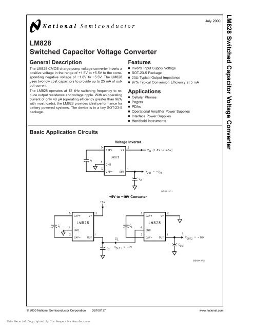
Basic Application Circuits<br />
Features<br />
n Inverts Input Supply <strong>Voltage</strong><br />
n SOT-23-5 Package<br />
n 20Ω Typical Output Impedance<br />
n 97% Typical Conversion Efficiency at 5 mA<br />
Applications<br />
n Cellular Phones<br />
n Pagers<br />
n PDAs<br />
n Operational Amplifier Power Supplies<br />
n Interface Power Supplies<br />
n Handheld Instruments<br />
<strong>Voltage</strong> Inverter<br />
July 2000<br />
<strong>LM828</strong> <strong>Switched</strong> <strong>Capacitor</strong> <strong>Voltage</strong> <strong>Converter</strong><br />
+5V to −10V <strong>Converter</strong><br />
DS100137-1<br />
DS100137-2<br />
© 2000 National Semiconductor Corporation DS100137 www.national.com
<strong>LM828</strong><br />
Absolute Maximum Ratings (Note 1)<br />
If Military/Aerospace specified devices are required,<br />
please contact the National Semiconductor Sales Office/<br />
Distributors for availability and specifications.<br />
Supply <strong>Voltage</strong> (V+ to<br />
GND, or GND to OUT)<br />
V+ and OUT Continuous<br />
Output Current<br />
Output Short-Circuit<br />
Duration to GND (Note 2)<br />
Continuous Power<br />
Dissipation (T A =<br />
25˚C)(Note 3)<br />
5.8V<br />
50 mA<br />
1 sec.<br />
240 mW<br />
T JMax (Note 3)<br />
θ JA (Note 3)<br />
Operating Junction<br />
Temperature Range<br />
Storage Temperature<br />
Range<br />
Lead Temp. (Soldering, 10<br />
seconds)<br />
ESD Rating (Note 7)<br />
150˚C<br />
300˚C/W<br />
−40˚C to 85˚C<br />
−65˚C to +150˚C<br />
300˚C<br />
2kV<br />
Electrical Characteristics<br />
Limits in standard typeface are for T J = 25˚C, and limits in boldface type apply over the full operating temperature range. Unless<br />
otherwise specified: V+ = 5V, C 1 =C 2 = 10 µF. (Note 4)<br />
Symbol Parameter Condition Min Typ Max Units<br />
V+ Supply <strong>Voltage</strong> R L =10kΩ 1.8 5.5 V<br />
I Q Supply Current No Load 40 75 µA<br />
115<br />
R OUT Output Resistance (Note 5) I L = 5 mA 20 65 Ω<br />
f OSC Oscillator Frequency (Note 6) Internal 12 24 56 kHz<br />
f SW Switching Frequency (Note 6) Measured at CAP+ 6 12 28 kHz<br />
P EFF Power Efficiency I L = 5 mA 97 %<br />
V OEFF <strong>Voltage</strong> Conversion Efficiency No Load 95 99.96 %<br />
Note 1: Absolute maximum ratings indicate limits beyond which damage to the device may occur. Electrical specifications do not apply when operating the device<br />
beyond its rated operating conditions.<br />
Note 2: OUT may be shorted to GND for one second without damage. However, shorting OUT to V+ may damage the device and should be avoided. Also, for temperatures<br />
above 85˚C, OUT must not be shorted to GND or V+, or the device may be damaged.<br />
Note 3: The maximum allowable power dissipation is calculated by using P DMax =(T JMax −T A )/θ JA , where T JMax is the maximum junction temperature, T A is the<br />
ambient temperature, and θ JA is the junction-to-ambient thermal resistance of the package.<br />
Note 4: In the test circuit, capacitors C 1 and C 2 are 10 µF, 0.3Ω maximum ESR capacitors. <strong>Capacitor</strong>s with higher ESR will increase output resistance, reduce output<br />
voltage and efficiency.<br />
Note 5: Specified output resistance includes internal switch resistance and capacitor ESR. See the details in the application information.<br />
Note 6: The output switches operate at one half of the oscillator frequency, f OSC =2f SW .<br />
Note 7: The human body model is a 100 pF capacitor discharged through a 1.5 kΩ resistor into each pin.<br />
www.national.com 2
Test Circuit<br />
<strong>LM828</strong><br />
*C 1 and C 2 are 10 µF capacitors.<br />
FIGURE 1. <strong>LM828</strong> Test Circuit<br />
DS100137-3<br />
Typical Performance Characteristics (Circuit of Figure 1, V+ = 5V unless otherwise specified)<br />
Supply Current vs<br />
Supply <strong>Voltage</strong><br />
Supply Current vs<br />
Temperature<br />
DS100137-29<br />
DS100137-30<br />
Output Source Resistance<br />
vs Supply <strong>Voltage</strong><br />
Output Source Resistance<br />
vs Temperature<br />
DS100137-31<br />
DS100137-32<br />
3<br />
www.national.com
<strong>LM828</strong><br />
Typical Performance Characteristics (Circuit of Figure 1, V+ = 5V unless otherwise<br />
specified) (Continued)<br />
Output <strong>Voltage</strong><br />
vs Load Current<br />
Efficiency vs<br />
Load Current<br />
DS100137-33<br />
DS100137-34<br />
Switching Frequency vs<br />
Supply <strong>Voltage</strong><br />
Switching Frequency vs<br />
Temperature<br />
DS100137-35<br />
DS100137-36<br />
Connection Diagram<br />
5-Lead Small Outline Package (M5)<br />
DS100137-14<br />
Actual Size<br />
DS100137-13<br />
Top View With Package Marking<br />
Ordering Information<br />
Order Number Package Package Marking<br />
Supplied as<br />
Number<br />
<strong>LM828</strong>M5 MA05B S08A (Note 8) Tape and Reel (250 units/rail)<br />
<strong>LM828</strong>M5X MA05B S08A (Note 8) Tape and Reel (3000 units/rail)<br />
Note 8: The first letter ″S″ identifies the part as a switched capacitor converter. The next two numbers are the device number. Larger quantity reels are available upon<br />
request.<br />
www.national.com 4
Pin Description<br />
Pin Name Function<br />
1 OUT Negative voltage output.<br />
2 V+ Power supply positive input.<br />
3 CAP− Connect this pin to the negative terminal of the charge-pump capacitor.<br />
4 GND Power supply ground input.<br />
5 CAP+ Connect this pin to the positive terminal of the charge-pump capacitor.<br />
<strong>LM828</strong><br />
Circuit Description<br />
The <strong>LM828</strong> contains four large CMOS switches which are<br />
switched in a sequence to invert the input supply voltage.<br />
Energy transfer and storage are provided by external capacitors.<br />
Figure 2 illustrates the voltage conversion scheme.<br />
When S 1 and S 3 are closed, C 1<br />
charges to the supply voltage<br />
V+. During this time interval, switches S 2 and S 4 are<br />
open. In the second time interval, S 1 and S 3 are open; at the<br />
same time, S 2 and S 4 are closed, C 1 is charging C 2 . After a<br />
number of cycles, the voltage across C 2 will be pumped to<br />
V+. Since the anode of C 2 is connected to ground, the output<br />
at the cathode of C 2 equals −(V+) when there is no load current.<br />
The output voltage drop when a load is added is determined<br />
by the parasitic resistance (R ds(on) of the MOSFET<br />
switches and the ESR of the capacitors) and the charge<br />
transfer loss between capacitors.<br />
a function of the ON resistance of the internal MOSFET<br />
switches, the oscillator frequency, the capacitance and the<br />
ESR of both C 1 and C 2 . Since the switching current charging<br />
and discharging C 1 is approximately twice as the output current,<br />
the effect of the ESR of the pumping capacitor C 1 will<br />
be multiplied by four in the output resistance. The output capacitor<br />
C 2 is charging and discharging at a current approximately<br />
equal to the output current, therefore, this ESR term<br />
only counts once in the output resistance. A good approximation<br />
of R out is:<br />
where R SW is the sum of the ON resistance of the internal<br />
MOSFET switches shown in Figure 2.<br />
High capacitance, low ESR capacitors will reduce the output<br />
resistance.<br />
The peak-to-peak output voltage ripple is determined by the<br />
oscillator frequency, the capacitance and ESR of the output<br />
capacitor C 2 :<br />
FIGURE 2. <strong>Voltage</strong> Inverting Principle<br />
Application Information<br />
DS100137-26<br />
Again, using a low ESR capacitor will result in lower ripple.<br />
<strong>Capacitor</strong> Selection<br />
The output resistance and ripple voltage are dependent on<br />
the capacitance and ESR values of the external capacitors.<br />
The output voltage drop is the load current times the output<br />
resistance, and the power efficiency is<br />
Simple Negative <strong>Voltage</strong> <strong>Converter</strong><br />
The main application of <strong>LM828</strong> is to generate a negative<br />
supply voltage. The voltage inverter circuit uses only two external<br />
capacitors as shown in the Basic Application Circuits.<br />
The range of the input supply voltage is 1.8V to 5.5V.<br />
The output characteristics of this circuit can be approximated<br />
by an ideal voltage source in series with a resistance. The<br />
voltage source equals −(V+). The output resistance, R out ,is<br />
Low ESR <strong>Capacitor</strong> Manufacturers<br />
Where I Q (V+) is the quiescent power loss of the IC device,<br />
and I 2 L R out is the conversion loss associated with the switch<br />
on-resistance, the two external capacitors and their ESRs.<br />
The selection of capacitors is based on the specifications of<br />
the dropout voltage (which equals I out R out ), the output voltage<br />
ripple, and the converter efficiency. Low ESR capacitors<br />
(following table) are recommended to maximize efficiency,<br />
reduce the output voltage drop and voltage ripple.<br />
Manufacturer Phone <strong>Capacitor</strong> Type<br />
Nichicon Corp. (708)-843-7500 PL & PF series, through-hole aluminum electrolytic<br />
AVX Corp. (803)-448-9411 TPS series, surface-mount tantalum<br />
Sprague (207)-324-4140 593D, 594D, 595D series, surface-mount tantalum<br />
Sanyo (619)-661-6835 OS-CON series, through-hole aluminum electrolytic<br />
5<br />
www.national.com
<strong>LM828</strong><br />
Application Information (Continued)<br />
Low ESR <strong>Capacitor</strong> Manufacturers (Continued)<br />
Manufacturer Phone <strong>Capacitor</strong> Type<br />
Murata (800)-831-9172 Ceramic chip capacitors<br />
Taiyo Yuden (800)-348-2496 Ceramic chip capacitors<br />
Tokin (408)-432-8020 Ceramic chip capacitors<br />
Other Applications<br />
Paralleling Devices<br />
Any number of <strong>LM828</strong>s can be paralleled to reduce the output<br />
resistance. Each device must have its own pumping capacitor<br />
C 1 , while only one output capacitor C out is needed as<br />
shown in Figure 3. The composite output resistance is:<br />
FIGURE 3. Lowering Output Resistance by Paralleling Devices<br />
DS100137-9<br />
Cascading Devices<br />
Cascading the <strong>LM828</strong>s is an easy way to produce a greater This can be seen by first assuming that each device is 100<br />
negative voltage (e.g. A two-stage cascade circuit is shown percent efficient. Since the output voltage is different on<br />
in Figure 4).<br />
each device the output current is as well. Each cascaded device<br />
sees less current at the output than the previous so the<br />
If n is the integer representing the number of devices cascaded,<br />
the unloaded output voltage V out is (-nV in ). The effective<br />
output resistance is equal to the weighted sum of each the number of n is practically limited since the increasing of<br />
R OUT voltage drop is lower in each device added. Note that,<br />
individual device:<br />
n significantly reduces the efficiency, and increases the output<br />
resistance and output voltage ripple.<br />
R out =nR out_1 + n/2 R out_2 +...+R out_n<br />
FIGURE 4. Increasing Output <strong>Voltage</strong> by Cascading Devices<br />
DS100137-10<br />
www.national.com 6
Other Applications (Continued)<br />
Combined Doubler and Inverter<br />
In Figure 5, the <strong>LM828</strong> is used to provide a positive voltage<br />
doubler and a negative voltage converter. Note that the total<br />
current drawn from the two outputs should not exceed 40<br />
mA.<br />
<strong>LM828</strong><br />
FIGURE 5. Combined <strong>Voltage</strong> Doubler and Inverter<br />
DS100137-11<br />
Regulating V OUT<br />
It is possible to regulate the negative output of the <strong>LM828</strong> by<br />
use of a low dropout regulator (such as the LP2980). The<br />
whole converter is depicted in Figure 6. This converter can<br />
give a regulated output from −1.8V to −5.5V by choosing the<br />
proper resistor ratio:<br />
V out =V ref (1+R 1 /R 2 )<br />
where, V ref = 1.23V<br />
Note that the following conditions must be satisfied simultaneously<br />
for worst case design:<br />
V in_min<br />
>V out_min +V drop_max (LP2980)<br />
+I out_max xR out_max (<strong>LM828</strong>)<br />
V in_max<br />
< V out_max +V drop_min (LP2980)<br />
+I out_min xR out_min (<strong>LM828</strong>)<br />
DS100137-12<br />
FIGURE 6. Combining <strong>LM828</strong> with LP2980 to Make a Negative Adjustable Regulator<br />
7<br />
www.national.com
<strong>LM828</strong> <strong>Switched</strong> <strong>Capacitor</strong> <strong>Voltage</strong> <strong>Converter</strong><br />
Physical Dimensions inches (millimeters) unless otherwise noted<br />
5-Lead Small Outline Package (M5)<br />
NS Package Number MF05A<br />
For Order Numbers, refer to the table in the ″Ordering Information″ section of this document.<br />
LIFE SUPPORT POLICY<br />
NATIONAL’S PRODUCTS ARE NOT AUTHORIZED FOR USE AS CRITICAL COMPONENTS IN LIFE SUPPORT<br />
DEVICES OR SYSTEMS WITHOUT THE EXPRESS WRITTEN APPROVAL OF THE PRESIDENT AND GENERAL<br />
COUNSEL OF NATIONAL SEMICONDUCTOR CORPORATION. As used herein:<br />
1. Life support devices or systems are devices or<br />
systems which, (a) are intended for surgical implant<br />
into the body, or (b) support or sustain life, and<br />
whose failure to perform when properly used in<br />
accordance with instructions for use provided in the<br />
labeling, can be reasonably expected to result in a<br />
significant injury to the user.<br />
2. A critical component is any component of a life<br />
support device or system whose failure to perform<br />
can be reasonably expected to cause the failure of<br />
the life support device or system, or to affect its<br />
safety or effectiveness.<br />
National Semiconductor<br />
Corporation<br />
Americas<br />
Tel: 1-800-272-9959<br />
Fax: 1-800-737-7018<br />
Email: support@nsc.com<br />
www.national.com<br />
National Semiconductor<br />
Europe<br />
Fax: +49 (0) 180-530 85 86<br />
Email: europe.support@nsc.com<br />
Deutsch Tel: +49 (0) 69 9508 6208<br />
English Tel: +44 (0) 870 24 0 2171<br />
Français Tel: +33 (0) 1 41 91 8790<br />
National Semiconductor<br />
Asia Pacific Customer<br />
Response Group<br />
Tel: 65-2544466<br />
Fax: 65-2504466<br />
Email: ap.support@nsc.com<br />
National Semiconductor<br />
Japan Ltd.<br />
Tel: 81-3-5639-7560<br />
Fax: 81-3-5639-7507<br />
National does not assume any responsibility for use of any circuitry described, no circuit patent licenses are implied and National reserves the right at any time without notice to change said circuitry and specifications.