Ultra-low-power 32-bit MCU ARM-based Cortex-M3, 384KB ... - Keil
Ultra-low-power 32-bit MCU ARM-based Cortex-M3, 384KB ... - Keil
Ultra-low-power 32-bit MCU ARM-based Cortex-M3, 384KB ... - Keil

Create successful ePaper yourself
Turn your PDF publications into a flip-book with our unique Google optimized e-Paper software.
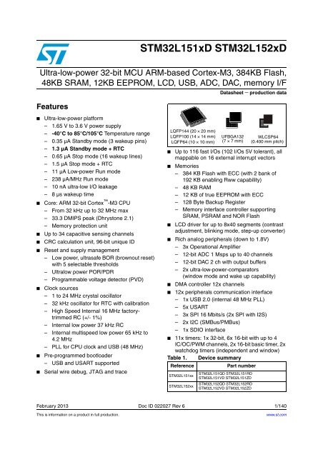
STM<strong>32</strong>L151xD STM<strong>32</strong>L152xD<br />
<strong>Ultra</strong>-<strong>low</strong>-<strong>power</strong> <strong>32</strong>-<strong>bit</strong> <strong>MCU</strong> <strong>ARM</strong>-<strong>based</strong> <strong>Cortex</strong>-<strong>M3</strong>, <strong>384KB</strong> Flash,<br />
48KB SRAM, 12KB EEPROM, LCD, USB, ADC, DAC, memory I/F<br />
Features<br />
Datasheet − production data<br />
■<br />
■<br />
■<br />
■<br />
■<br />
■<br />
■<br />
■<br />
<strong>Ultra</strong>-<strong>low</strong>-<strong>power</strong> platform<br />
– 1.65 V to 3.6 V <strong>power</strong> supply<br />
– -40°C to 85°C/105°C Temperature range<br />
– 0.35 µA Standby mode (3 wakeup pins)<br />
– 1.3 µA Standby mode + RTC<br />
– 0.65 µA Stop mode (16 wakeup lines)<br />
– 1.5 µA Stop mode + RTC<br />
– 11 µA Low-<strong>power</strong> Run mode<br />
– 238 µA/MHz Run mode<br />
– 10 nA ultra-<strong>low</strong> I/O leakage<br />
– 8 µs wakeup time<br />
Core: <strong>ARM</strong> <strong>32</strong>-<strong>bit</strong> <strong>Cortex</strong> -<strong>M3</strong> CPU<br />
– From <strong>32</strong> kHz up to <strong>32</strong> MHz max<br />
– 33.3 DMIPS peak (Dhrystone 2.1)<br />
– Memory protection unit<br />
Up to 34 capacitive sensing channels<br />
CRC calculation unit, 96-<strong>bit</strong> unique ID<br />
Reset and supply management<br />
– Low <strong>power</strong>, ultrasafe BOR (brownout reset)<br />
with 5 selectable thresholds<br />
– <strong>Ultra</strong><strong>low</strong> <strong>power</strong> POR/PDR<br />
– Programmable voltage detector (PVD)<br />
Clock sources<br />
– 1 to 24 MHz crystal oscillator<br />
– <strong>32</strong> kHz oscillator for RTC with calibration<br />
– High Speed Internal 16 MHz factorytrimmed<br />
RC (+/- 1%)<br />
– Internal <strong>low</strong> <strong>power</strong> 37 kHz RC<br />
– Internal multispeed <strong>low</strong> <strong>power</strong> 65 kHz to<br />
4.2 MHz<br />
– PLL for CPU clock and USB (48 MHz)<br />
Pre-programmed bootloader<br />
– USB and USART supported<br />
Serial wire debug, JTAG and trace<br />
LQFP144 (20 × 20 mm)<br />
LQFP100 (14 × 14 mm)<br />
LQFP64 (10 × 10 mm)<br />
■ Up to 116 fast I/Os (102 I/Os 5V tolerant), all<br />
mappable on 16 external interrupt vectors<br />
■ Memories<br />
– 384 KB Flash with ECC (with 2 bank of<br />
192 KB enabling Rww capability)<br />
– 48 KB RAM<br />
– 12 KB of true EEPROM with ECC<br />
– 128 Byte Backup Register<br />
– Memory interface controller supporting<br />
SRAM, PSRAM and NOR Flash<br />
■ LCD driver for up to 8x40 segments (contrast<br />
adjustment, blinking mode, step-up converter)<br />
■ Rich analog peripherals (down to 1.8V)<br />
– 3x Operational Amplifier<br />
– 12-<strong>bit</strong> ADC 1 Msps up to 40 channels<br />
– 12-<strong>bit</strong> DAC 2 ch with output buffers<br />
– 2x ultra-<strong>low</strong>-<strong>power</strong>-comparators<br />
(window mode and wake up capability)<br />
■ DMA controller 12x channels<br />
■ 12x peripherals communication interface<br />
– 1x USB 2.0 (internal 48 MHz PLL)<br />
– 5x USART<br />
– 3x SPI 16 M<strong>bit</strong>s/s (2x SPI with I2S)<br />
– 2x I2C (SMBus/PMBus)<br />
– 1x SDIO interface<br />
■ 11x timers: 1x <strong>32</strong>-<strong>bit</strong>, 6x 16-<strong>bit</strong> with up to 4<br />
IC/OC/PWM channels, 2x 16-<strong>bit</strong> basic timer, 2x<br />
watchdog timers (independent and window)<br />
Table 1. Device summary<br />
Reference<br />
Part number<br />
STM<strong>32</strong>L151xx<br />
STM<strong>32</strong>L152xx<br />
UFBGA1<strong>32</strong><br />
(7 × 7 mm)<br />
STM<strong>32</strong>L151QD STM<strong>32</strong>L151RD<br />
STM<strong>32</strong>L151VD STM<strong>32</strong>L151ZD<br />
STM<strong>32</strong>L152QD STM<strong>32</strong>L152RD<br />
STM<strong>32</strong>L152VD STM<strong>32</strong>L152ZD<br />
WLCSP64<br />
(0.400 mm pitch)<br />
February 2013 Doc ID 022027 Rev 6 1/140<br />
This is information on a product in full production.<br />
www.st.com<br />
1
Contents<br />
STM<strong>32</strong>L151xD STM<strong>32</strong>L152xD<br />
Contents<br />
1 Introduction . . . . . . . . . . . . . . . . . . . . . . . . . . . . . . . . . . . . . . . . . . . . . . . . 9<br />
2 Description . . . . . . . . . . . . . . . . . . . . . . . . . . . . . . . . . . . . . . . . . . . . . . . . 10<br />
2.1 Device overview . . . . . . . . . . . . . . . . . . . . . . . . . . . . . . . . . . . . . . . . . . . . 11<br />
2.2 <strong>Ultra</strong>-<strong>low</strong>-<strong>power</strong> device continuum . . . . . . . . . . . . . . . . . . . . . . . . . . . . . . 12<br />
2.2.1 Performance . . . . . . . . . . . . . . . . . . . . . . . . . . . . . . . . . . . . . . . . . . . . . 12<br />
2.2.2 Shared peripherals . . . . . . . . . . . . . . . . . . . . . . . . . . . . . . . . . . . . . . . . 12<br />
2.2.3 Common system strategy . . . . . . . . . . . . . . . . . . . . . . . . . . . . . . . . . . . 12<br />
2.2.4 Features . . . . . . . . . . . . . . . . . . . . . . . . . . . . . . . . . . . . . . . . . . . . . . . . . 12<br />
3 Functional overview . . . . . . . . . . . . . . . . . . . . . . . . . . . . . . . . . . . . . . . . 13<br />
3.1 Low <strong>power</strong> modes . . . . . . . . . . . . . . . . . . . . . . . . . . . . . . . . . . . . . . . . . . 14<br />
3.2 <strong>ARM</strong> ® <strong>Cortex</strong>-<strong>M3</strong> core with MPU . . . . . . . . . . . . . . . . . . . . . . . . . . . . . 18<br />
3.3 Reset and supply management . . . . . . . . . . . . . . . . . . . . . . . . . . . . . . . . 19<br />
3.3.1 Power supply schemes . . . . . . . . . . . . . . . . . . . . . . . . . . . . . . . . . . . . . 19<br />
3.3.2 Power supply supervisor . . . . . . . . . . . . . . . . . . . . . . . . . . . . . . . . . . . . 19<br />
3.3.3 Voltage regulator . . . . . . . . . . . . . . . . . . . . . . . . . . . . . . . . . . . . . . . . . . 20<br />
3.3.4 Boot modes . . . . . . . . . . . . . . . . . . . . . . . . . . . . . . . . . . . . . . . . . . . . . . 20<br />
3.4 Clock management . . . . . . . . . . . . . . . . . . . . . . . . . . . . . . . . . . . . . . . . . 21<br />
3.5 Low <strong>power</strong> real-time clock and backup registers . . . . . . . . . . . . . . . . . . . 23<br />
3.6 GPIOs (general-purpose inputs/outputs) . . . . . . . . . . . . . . . . . . . . . . . . . 23<br />
3.7 Memories . . . . . . . . . . . . . . . . . . . . . . . . . . . . . . . . . . . . . . . . . . . . . . . . . 24<br />
3.8 FSMC (flexible static memory controller) . . . . . . . . . . . . . . . . . . . . . . . . . 24<br />
3.9 DMA (direct memory access) . . . . . . . . . . . . . . . . . . . . . . . . . . . . . . . . . . 24<br />
3.10 LCD (liquid crystal display) . . . . . . . . . . . . . . . . . . . . . . . . . . . . . . . . . . . . 25<br />
3.11 ADC (analog-to-digital converter) . . . . . . . . . . . . . . . . . . . . . . . . . . . . . . . 25<br />
3.11.1 Temperature sensor . . . . . . . . . . . . . . . . . . . . . . . . . . . . . . . . . . . . . . . . 25<br />
3.11.2 Internal voltage reference (V REFINT ) . . . . . . . . . . . . . . . . . . . . . . . . . . . 26<br />
3.12 DAC (digital-to-analog converter) . . . . . . . . . . . . . . . . . . . . . . . . . . . . . . . 26<br />
3.13 Operational amplifier . . . . . . . . . . . . . . . . . . . . . . . . . . . . . . . . . . . . . . . . 27<br />
3.14 <strong>Ultra</strong>-<strong>low</strong>-<strong>power</strong> comparators and reference voltage . . . . . . . . . . . . . . . . 27<br />
3.15 System configuration controller and routing interface . . . . . . . . . . . . . . . 27<br />
2/140 Doc ID 022027 Rev 6
STM<strong>32</strong>L151xD STM<strong>32</strong>L152xD<br />
Contents<br />
3.16 Touch sensing . . . . . . . . . . . . . . . . . . . . . . . . . . . . . . . . . . . . . . . . . . . . . 27<br />
3.17 Timers and watchdogs . . . . . . . . . . . . . . . . . . . . . . . . . . . . . . . . . . . . . . . 28<br />
3.17.1 General-purpose timers (TIM2, TI<strong>M3</strong>, TIM4, TIM5, TIM9, TIM10 and<br />
TIM11) . . . . . . . . . . . . . . . . . . . . . . . . . . . . . . . . . . . . . . . . . . . . . . . . . . 28<br />
3.17.2 Basic timers (TIM6 and TIM7) . . . . . . . . . . . . . . . . . . . . . . . . . . . . . . . . 29<br />
3.17.3 SysTick timer . . . . . . . . . . . . . . . . . . . . . . . . . . . . . . . . . . . . . . . . . . . . . 29<br />
3.17.4 Independent watchdog (IWDG) . . . . . . . . . . . . . . . . . . . . . . . . . . . . . . . 29<br />
3.17.5 Window watchdog (WWDG) . . . . . . . . . . . . . . . . . . . . . . . . . . . . . . . . . 29<br />
3.18 Communication interfaces . . . . . . . . . . . . . . . . . . . . . . . . . . . . . . . . . . . . 29<br />
3.18.1 I²C bus . . . . . . . . . . . . . . . . . . . . . . . . . . . . . . . . . . . . . . . . . . . . . . . . . . 29<br />
3.18.2 Universal synchronous/asynchronous receiver transmitter (USART) . . 30<br />
3.18.3 Serial peripheral interface (SPI) . . . . . . . . . . . . . . . . . . . . . . . . . . . . . . . 30<br />
3.18.4 Inter-integrated sound (I2S) . . . . . . . . . . . . . . . . . . . . . . . . . . . . . . . . . . 30<br />
3.18.5 SDIO . . . . . . . . . . . . . . . . . . . . . . . . . . . . . . . . . . . . . . . . . . . . . . . . . . . 30<br />
3.18.6 Universal serial bus (USB) . . . . . . . . . . . . . . . . . . . . . . . . . . . . . . . . . . . 30<br />
3.19 CRC (cyclic redundancy check) calculation unit . . . . . . . . . . . . . . . . . . . 31<br />
3.20 Development support . . . . . . . . . . . . . . . . . . . . . . . . . . . . . . . . . . . . . . . . 31<br />
4 Pin descriptions . . . . . . . . . . . . . . . . . . . . . . . . . . . . . . . . . . . . . . . . . . . <strong>32</strong><br />
5 Memory mapping . . . . . . . . . . . . . . . . . . . . . . . . . . . . . . . . . . . . . . . . . . 52<br />
6 Electrical characteristics . . . . . . . . . . . . . . . . . . . . . . . . . . . . . . . . . . . . 53<br />
6.1 Parameter conditions . . . . . . . . . . . . . . . . . . . . . . . . . . . . . . . . . . . . . . . . 53<br />
6.1.1 Minimum and maximum values . . . . . . . . . . . . . . . . . . . . . . . . . . . . . . . 53<br />
6.1.2 Typical values . . . . . . . . . . . . . . . . . . . . . . . . . . . . . . . . . . . . . . . . . . . . . 53<br />
6.1.3 Typical curves . . . . . . . . . . . . . . . . . . . . . . . . . . . . . . . . . . . . . . . . . . . . 53<br />
6.1.4 Loading capacitor . . . . . . . . . . . . . . . . . . . . . . . . . . . . . . . . . . . . . . . . . 53<br />
6.1.5 Pin input voltage . . . . . . . . . . . . . . . . . . . . . . . . . . . . . . . . . . . . . . . . . . 53<br />
6.1.6 Power supply scheme . . . . . . . . . . . . . . . . . . . . . . . . . . . . . . . . . . . . . . 54<br />
6.1.7 Current consumption measurement . . . . . . . . . . . . . . . . . . . . . . . . . . . 54<br />
6.2 Absolute maximum ratings . . . . . . . . . . . . . . . . . . . . . . . . . . . . . . . . . . . . 55<br />
6.3 Operating conditions . . . . . . . . . . . . . . . . . . . . . . . . . . . . . . . . . . . . . . . . 56<br />
6.3.1 General operating conditions . . . . . . . . . . . . . . . . . . . . . . . . . . . . . . . . . 56<br />
6.3.2 Embedded reset and <strong>power</strong> control block characteristics . . . . . . . . . . . 56<br />
6.3.3 Embedded internal reference voltage . . . . . . . . . . . . . . . . . . . . . . . . . . 59<br />
6.3.4 Supply current characteristics . . . . . . . . . . . . . . . . . . . . . . . . . . . . . . . . 60<br />
Doc ID 022027 Rev 6 3/140
Contents<br />
STM<strong>32</strong>L151xD STM<strong>32</strong>L152xD<br />
6.3.5 External clock source characteristics . . . . . . . . . . . . . . . . . . . . . . . . . . . 71<br />
6.3.6 Internal clock source characteristics . . . . . . . . . . . . . . . . . . . . . . . . . . . 78<br />
6.3.7 PLL characteristics . . . . . . . . . . . . . . . . . . . . . . . . . . . . . . . . . . . . . . . . 81<br />
6.3.8 Memory characteristics . . . . . . . . . . . . . . . . . . . . . . . . . . . . . . . . . . . . . 81<br />
6.3.9 FSMC characteristics . . . . . . . . . . . . . . . . . . . . . . . . . . . . . . . . . . . . . . . 83<br />
6.3.10 EMC characteristics . . . . . . . . . . . . . . . . . . . . . . . . . . . . . . . . . . . . . . . . 94<br />
6.3.11 Absolute maximum ratings (electrical sensitivity) . . . . . . . . . . . . . . . . . 95<br />
6.3.12 I/O current injection characteristics . . . . . . . . . . . . . . . . . . . . . . . . . . . . 96<br />
6.3.13 I/O port characteristics . . . . . . . . . . . . . . . . . . . . . . . . . . . . . . . . . . . . . . 97<br />
6.3.14 NRST pin characteristics . . . . . . . . . . . . . . . . . . . . . . . . . . . . . . . . . . . 100<br />
6.3.15 TIM timer characteristics . . . . . . . . . . . . . . . . . . . . . . . . . . . . . . . . . . . 101<br />
6.3.16 Communications interfaces . . . . . . . . . . . . . . . . . . . . . . . . . . . . . . . . . 102<br />
6.3.17 I2S characteristics . . . . . . . . . . . . . . . . . . . . . . . . . . . . . . . . . . . . . . . . 107<br />
6.3.18 SDIO characteristics . . . . . . . . . . . . . . . . . . . . . . . . . . . . . . . . . . . . . . 109<br />
6.3.19 12-<strong>bit</strong> ADC characteristics . . . . . . . . . . . . . . . . . . . . . . . . . . . . . . . . . . 111<br />
6.3.20 DAC electrical specifications . . . . . . . . . . . . . . . . . . . . . . . . . . . . . . . . 117<br />
6.3.21 Operational amplifier characteristics . . . . . . . . . . . . . . . . . . . . . . . . . . 119<br />
6.3.22 Temperature sensor characteristics . . . . . . . . . . . . . . . . . . . . . . . . . . . 121<br />
6.3.23 Comparator . . . . . . . . . . . . . . . . . . . . . . . . . . . . . . . . . . . . . . . . . . . . . 121<br />
6.3.24 LCD controller (STM<strong>32</strong>L152xD only) . . . . . . . . . . . . . . . . . . . . . . . . . . 123<br />
7 Package characteristics . . . . . . . . . . . . . . . . . . . . . . . . . . . . . . . . . . . . 124<br />
7.1 Package mechanical data . . . . . . . . . . . . . . . . . . . . . . . . . . . . . . . . . . . 124<br />
7.2 Thermal characteristics . . . . . . . . . . . . . . . . . . . . . . . . . . . . . . . . . . . . . 134<br />
7.2.1 Reference document . . . . . . . . . . . . . . . . . . . . . . . . . . . . . . . . . . . . . . 135<br />
8 Ordering information scheme . . . . . . . . . . . . . . . . . . . . . . . . . . . . . . . 136<br />
9 Revision history . . . . . . . . . . . . . . . . . . . . . . . . . . . . . . . . . . . . . . . . . . 137<br />
4/140 Doc ID 022027 Rev 6
STM<strong>32</strong>L151xD STM<strong>32</strong>L152xD<br />
List of tables<br />
List of tables<br />
Table 1. Device summary . . . . . . . . . . . . . . . . . . . . . . . . . . . . . . . . . . . . . . . . . . . . . . . . . . . . . . . . . . 1<br />
Table 2. <strong>Ultra</strong>-<strong>low</strong>-<strong>power</strong> STM<strong>32</strong>L15xxD device features and peripheral counts. . . . . . . . . . . . . . . 11<br />
Table 3. Functionalities depending on the operating <strong>power</strong> supply range . . . . . . . . . . . . . . . . . . . . 16<br />
Table 4. CPU frequency range depending on dynamic voltage scaling . . . . . . . . . . . . . . . . . . . . . . 16<br />
Table 5.<br />
Functionalities depending on the working mode (from Run/active down to<br />
standby) . . . . . . . . . . . . . . . . . . . . . . . . . . . . . . . . . . . . . . . . . . . . . . . . . . . . . . . . . . . . . . . 17<br />
Table 6. Temperature sensor calibration values. . . . . . . . . . . . . . . . . . . . . . . . . . . . . . . . . . . . . . . . 26<br />
Table 7. Internal voltage reference measured values. . . . . . . . . . . . . . . . . . . . . . . . . . . . . . . . . . . . 26<br />
Table 8. Timer feature comparison. . . . . . . . . . . . . . . . . . . . . . . . . . . . . . . . . . . . . . . . . . . . . . . . . . 28<br />
Table 9. STM<strong>32</strong>L15xxD pin definitions . . . . . . . . . . . . . . . . . . . . . . . . . . . . . . . . . . . . . . . . . . . . . . . 37<br />
Table 10. Alternate function input/output . . . . . . . . . . . . . . . . . . . . . . . . . . . . . . . . . . . . . . . . . . . . . . 43<br />
Table 11. Voltage characteristics . . . . . . . . . . . . . . . . . . . . . . . . . . . . . . . . . . . . . . . . . . . . . . . . . . . . 55<br />
Table 12. Current characteristics . . . . . . . . . . . . . . . . . . . . . . . . . . . . . . . . . . . . . . . . . . . . . . . . . . . . 55<br />
Table 13. Thermal characteristics. . . . . . . . . . . . . . . . . . . . . . . . . . . . . . . . . . . . . . . . . . . . . . . . . . . . 56<br />
Table 14. General operating conditions . . . . . . . . . . . . . . . . . . . . . . . . . . . . . . . . . . . . . . . . . . . . . . . 56<br />
Table 15. Embedded reset and <strong>power</strong> control block characteristics. . . . . . . . . . . . . . . . . . . . . . . . . . 57<br />
Table 16. Embedded internal reference voltage. . . . . . . . . . . . . . . . . . . . . . . . . . . . . . . . . . . . . . . . . 59<br />
Table 17. Current consumption in Run mode, code with data processing running from Flash. . . . . . 60<br />
Table 18. Current consumption in Run mode, code with data processing running from RAM . . . . . . 61<br />
Table 19. Current consumption in Sleep mode . . . . . . . . . . . . . . . . . . . . . . . . . . . . . . . . . . . . . . . . . 62<br />
Table 20. Current consumption in Low <strong>power</strong> run mode . . . . . . . . . . . . . . . . . . . . . . . . . . . . . . . . . . 63<br />
Table 21. Current consumption in Low <strong>power</strong> sleep mode. . . . . . . . . . . . . . . . . . . . . . . . . . . . . . . . . 64<br />
Table 22. Typical and maximum current consumptions in Stop mode . . . . . . . . . . . . . . . . . . . . . . . . 65<br />
Table 23. Typical and maximum current consumptions in Standby mode . . . . . . . . . . . . . . . . . . . . . 66<br />
Table 24. Typical and maximum timings in Low <strong>power</strong> modes. . . . . . . . . . . . . . . . . . . . . . . . . . . . . . 68<br />
Table 25. Peripheral current consumption . . . . . . . . . . . . . . . . . . . . . . . . . . . . . . . . . . . . . . . . . . . . . 69<br />
Table 26. High-speed external user clock characteristics. . . . . . . . . . . . . . . . . . . . . . . . . . . . . . . . . . 71<br />
Table 27. Low-speed external user clock characteristics . . . . . . . . . . . . . . . . . . . . . . . . . . . . . . . . . . 73<br />
Table 28. HSE 1-24 MHz oscillator characteristics. . . . . . . . . . . . . . . . . . . . . . . . . . . . . . . . . . . . . . . 75<br />
Table 29. LSE oscillator characteristics (f LSE = <strong>32</strong>.768 kHz) . . . . . . . . . . . . . . . . . . . . . . . . . . . . . . . 76<br />
Table 30. HSI oscillator characteristics. . . . . . . . . . . . . . . . . . . . . . . . . . . . . . . . . . . . . . . . . . . . . . . . 78<br />
Table 31. LSI oscillator characteristics . . . . . . . . . . . . . . . . . . . . . . . . . . . . . . . . . . . . . . . . . . . . . . . . 78<br />
Table <strong>32</strong>. MSI oscillator characteristics . . . . . . . . . . . . . . . . . . . . . . . . . . . . . . . . . . . . . . . . . . . . . . . 79<br />
Table 33. PLL characteristics . . . . . . . . . . . . . . . . . . . . . . . . . . . . . . . . . . . . . . . . . . . . . . . . . . . . . . . 81<br />
Table 34. RAM and hardware registers . . . . . . . . . . . . . . . . . . . . . . . . . . . . . . . . . . . . . . . . . . . . . . . 81<br />
Table 35. Flash memory and data EEPROM characteristics . . . . . . . . . . . . . . . . . . . . . . . . . . . . . . . 82<br />
Table 36. Flash memory and data EEPROM endurance and retention . . . . . . . . . . . . . . . . . . . . . . . 82<br />
Table 37. Asynchronous non-multiplexed SRAM/PSRAM/NOR read timings . . . . . . . . . . . . . . . . . . 84<br />
Table 38. Asynchronous non-multiplexed SRAM/PSRAM/NOR write timings . . . . . . . . . . . . . . . . . . 85<br />
Table 39. Asynchronous multiplexed PSRAM/NOR read timings. . . . . . . . . . . . . . . . . . . . . . . . . . . . 86<br />
Table 40. Asynchronous multiplexed PSRAM/NOR write timings . . . . . . . . . . . . . . . . . . . . . . . . . . . 87<br />
Table 41. Synchronous multiplexed NOR/PSRAM read timings . . . . . . . . . . . . . . . . . . . . . . . . . . . . 89<br />
Table 42. Synchronous multiplexed PSRAM write timings. . . . . . . . . . . . . . . . . . . . . . . . . . . . . . . . . 91<br />
Table 43. Synchronous non-multiplexed NOR/PSRAM read timings . . . . . . . . . . . . . . . . . . . . . . . . . 92<br />
Table 44. Synchronous non-multiplexed PSRAM write timings . . . . . . . . . . . . . . . . . . . . . . . . . . . . . 93<br />
Table 45. EMS characteristics . . . . . . . . . . . . . . . . . . . . . . . . . . . . . . . . . . . . . . . . . . . . . . . . . . . . . . 94<br />
Table 46. EMI characteristics . . . . . . . . . . . . . . . . . . . . . . . . . . . . . . . . . . . . . . . . . . . . . . . . . . . . . . . 95<br />
Table 47. ESD absolute maximum ratings . . . . . . . . . . . . . . . . . . . . . . . . . . . . . . . . . . . . . . . . . . . . . 95<br />
Doc ID 022027 Rev 6 5/140
List of tables<br />
STM<strong>32</strong>L151xD STM<strong>32</strong>L152xD<br />
Table 48. Electrical sensitivities . . . . . . . . . . . . . . . . . . . . . . . . . . . . . . . . . . . . . . . . . . . . . . . . . . . . . 96<br />
Table 49. I/O current injection susceptibility . . . . . . . . . . . . . . . . . . . . . . . . . . . . . . . . . . . . . . . . . . . . 96<br />
Table 50. I/O static characteristics . . . . . . . . . . . . . . . . . . . . . . . . . . . . . . . . . . . . . . . . . . . . . . . . . . . 97<br />
Table 51. Output voltage characteristics . . . . . . . . . . . . . . . . . . . . . . . . . . . . . . . . . . . . . . . . . . . . . . 98<br />
Table 52. I/O AC characteristics . . . . . . . . . . . . . . . . . . . . . . . . . . . . . . . . . . . . . . . . . . . . . . . . . . . . . 99<br />
Table 53. NRST pin characteristics . . . . . . . . . . . . . . . . . . . . . . . . . . . . . . . . . . . . . . . . . . . . . . . . . 100<br />
Table 54. TIMx characteristics . . . . . . . . . . . . . . . . . . . . . . . . . . . . . . . . . . . . . . . . . . . . . . . . . . . . . 101<br />
Table 55. I 2 C characteristics. . . . . . . . . . . . . . . . . . . . . . . . . . . . . . . . . . . . . . . . . . . . . . . . . . . . . . . 102<br />
Table 56. SCL frequency (f PCLK1 = <strong>32</strong> MHz, V DD = 3.3 V) . . . . . . . . . . . . . . . . . . . . . . . . . . . . . . . . 103<br />
Table 57. SPI characteristics . . . . . . . . . . . . . . . . . . . . . . . . . . . . . . . . . . . . . . . . . . . . . . . . . . . . . . 104<br />
Table 58. I2S characteristics . . . . . . . . . . . . . . . . . . . . . . . . . . . . . . . . . . . . . . . . . . . . . . . . . . . . . . 107<br />
Table 59. SDIO characteristics . . . . . . . . . . . . . . . . . . . . . . . . . . . . . . . . . . . . . . . . . . . . . . . . . . . . . 109<br />
Table 60. USB startup time. . . . . . . . . . . . . . . . . . . . . . . . . . . . . . . . . . . . . . . . . . . . . . . . . . . . . . . . 110<br />
Table 61. USB DC electrical characteristics . . . . . . . . . . . . . . . . . . . . . . . . . . . . . . . . . . . . . . . . . . . 110<br />
Table 62. USB: full speed electrical characteristics . . . . . . . . . . . . . . . . . . . . . . . . . . . . . . . . . . . . . 110<br />
Table 63. ADC clock frequency . . . . . . . . . . . . . . . . . . . . . . . . . . . . . . . . . . . . . . . . . . . . . . . . . . . . 111<br />
Table 64. ADC characteristics . . . . . . . . . . . . . . . . . . . . . . . . . . . . . . . . . . . . . . . . . . . . . . . . . . . . . 111<br />
Table 65. ADC accuracy. . . . . . . . . . . . . . . . . . . . . . . . . . . . . . . . . . . . . . . . . . . . . . . . . . . . . . . . . . 113<br />
Table 66. R AIN max for f ADC = 16 MHz. . . . . . . . . . . . . . . . . . . . . . . . . . . . . . . . . . . . . . . . . . . . . . . 115<br />
Table 67. DAC characteristics . . . . . . . . . . . . . . . . . . . . . . . . . . . . . . . . . . . . . . . . . . . . . . . . . . . . . 117<br />
Table 68. Operational amplifier characteristics. . . . . . . . . . . . . . . . . . . . . . . . . . . . . . . . . . . . . . . . . 119<br />
Table 69. Temperature sensor characteristics . . . . . . . . . . . . . . . . . . . . . . . . . . . . . . . . . . . . . . . . . 121<br />
Table 70. Comparator 1 characteristics . . . . . . . . . . . . . . . . . . . . . . . . . . . . . . . . . . . . . . . . . . . . . . 121<br />
Table 71. Comparator 2 characteristics . . . . . . . . . . . . . . . . . . . . . . . . . . . . . . . . . . . . . . . . . . . . . . 122<br />
Table 72. LCD controller characteristics. . . . . . . . . . . . . . . . . . . . . . . . . . . . . . . . . . . . . . . . . . . . . . 123<br />
Table 73. LQFP144, 20 x 20 mm, 144-pin <strong>low</strong>-profile quad flat package mechanical data . . . . . . . 126<br />
Table 74. LQPF100, 14 x 14 mm, 100-pin <strong>low</strong>-profile quad flat package mechanical data . . . . . . . 128<br />
Table 75. LQFP64, 10 x 10 mm 64-pin <strong>low</strong>-profile quad flat package mechanical data. . . . . . . . . . 130<br />
Table 76. UFBGA1<strong>32</strong>, 7 x 7 mm, 1<strong>32</strong>-ball ultra thin, fine-pitch ball grid array mechanical data. . . . 131<br />
Table 77. WLCSP64, 0.400 mm pitch wafer level chip size package mechanical data . . . . . . . . . . 133<br />
Table 78. Thermal characteristics. . . . . . . . . . . . . . . . . . . . . . . . . . . . . . . . . . . . . . . . . . . . . . . . . . . 134<br />
Table 79. STM<strong>32</strong>L15xxD ordering information scheme . . . . . . . . . . . . . . . . . . . . . . . . . . . . . . . . . . 136<br />
6/140 Doc ID 022027 Rev 6
STM<strong>32</strong>L151xD STM<strong>32</strong>L152xD<br />
List of figures<br />
List of figures<br />
Figure 1. <strong>Ultra</strong>-<strong>low</strong>-<strong>power</strong> STM<strong>32</strong>L15xxD block diagram . . . . . . . . . . . . . . . . . . . . . . . . . . . . . . . . . 13<br />
Figure 2. Clock tree . . . . . . . . . . . . . . . . . . . . . . . . . . . . . . . . . . . . . . . . . . . . . . . . . . . . . . . . . . . . . . 22<br />
Figure 3. STM<strong>32</strong>L15xZD LQFP144 pinout . . . . . . . . . . . . . . . . . . . . . . . . . . . . . . . . . . . . . . . . . . . . <strong>32</strong><br />
Figure 4. STM<strong>32</strong>L15xQD UFBGA1<strong>32</strong> ballout . . . . . . . . . . . . . . . . . . . . . . . . . . . . . . . . . . . . . . . . . . 33<br />
Figure 5. STM<strong>32</strong>L15xVD LQFP100 pinout . . . . . . . . . . . . . . . . . . . . . . . . . . . . . . . . . . . . . . . . . . . . 34<br />
Figure 6. STM<strong>32</strong>L15xRD LQFP64 pinout . . . . . . . . . . . . . . . . . . . . . . . . . . . . . . . . . . . . . . . . . . . . . 35<br />
Figure 7. STM<strong>32</strong>L15xRD WLCSP64 ballout . . . . . . . . . . . . . . . . . . . . . . . . . . . . . . . . . . . . . . . . . . . 36<br />
Figure 8. Memory map . . . . . . . . . . . . . . . . . . . . . . . . . . . . . . . . . . . . . . . . . . . . . . . . . . . . . . . . . . . 52<br />
Figure 9. Pin loading conditions. . . . . . . . . . . . . . . . . . . . . . . . . . . . . . . . . . . . . . . . . . . . . . . . . . . . . 53<br />
Figure 10. Pin input voltage . . . . . . . . . . . . . . . . . . . . . . . . . . . . . . . . . . . . . . . . . . . . . . . . . . . . . . . . . 53<br />
Figure 11. Power supply scheme. . . . . . . . . . . . . . . . . . . . . . . . . . . . . . . . . . . . . . . . . . . . . . . . . . . . . 54<br />
Figure 12. Current consumption measurement scheme . . . . . . . . . . . . . . . . . . . . . . . . . . . . . . . . . . . 54<br />
Figure 13. Low-speed external clock source AC timing diagram. . . . . . . . . . . . . . . . . . . . . . . . . . . . . 73<br />
Figure 14. High-speed external clock source AC timing diagram . . . . . . . . . . . . . . . . . . . . . . . . . . . . 74<br />
Figure 15. HSE oscillator circuit diagram. . . . . . . . . . . . . . . . . . . . . . . . . . . . . . . . . . . . . . . . . . . . . . . 76<br />
Figure 16. Typical application with a <strong>32</strong>.768 kHz crystal . . . . . . . . . . . . . . . . . . . . . . . . . . . . . . . . . . . 77<br />
Figure 17. Asynchronous non-multiplexed SRAM/PSRAM/NOR read waveforms . . . . . . . . . . . . . . . 83<br />
Figure 18. Asynchronous non-multiplexed SRAM/PSRAM/NOR write waveforms . . . . . . . . . . . . . . . 84<br />
Figure 19. Asynchronous multiplexed PSRAM/NOR read waveforms. . . . . . . . . . . . . . . . . . . . . . . . . 85<br />
Figure 20. Asynchronous multiplexed PSRAM/NOR write waveforms . . . . . . . . . . . . . . . . . . . . . . . . 86<br />
Figure 21. Synchronous multiplexed NOR/PSRAM read timings . . . . . . . . . . . . . . . . . . . . . . . . . . . . 88<br />
Figure 22. Synchronous multiplexed PSRAM write timings. . . . . . . . . . . . . . . . . . . . . . . . . . . . . . . . . 90<br />
Figure 23. Synchronous non-multiplexed NOR/PSRAM read timings . . . . . . . . . . . . . . . . . . . . . . . . . 92<br />
Figure 24. Synchronous non-multiplexed PSRAM write timings . . . . . . . . . . . . . . . . . . . . . . . . . . . . . 93<br />
Figure 25. I/O AC characteristics definition . . . . . . . . . . . . . . . . . . . . . . . . . . . . . . . . . . . . . . . . . . . . 100<br />
Figure 26. Recommended NRST pin protection . . . . . . . . . . . . . . . . . . . . . . . . . . . . . . . . . . . . . . . . 101<br />
Figure 27. I 2 C bus AC waveforms and measurement circuit . . . . . . . . . . . . . . . . . . . . . . . . . . . . . . . 103<br />
Figure 28. SPI timing diagram - slave mode and CPHA = 0 . . . . . . . . . . . . . . . . . . . . . . . . . . . . . . . 105<br />
Figure 29. SPI timing diagram - slave mode and CPHA = 1 (1) . . . . . . . . . . . . . . . . . . . . . . . . . . . . . 105<br />
Figure 30. SPI timing diagram - master mode (1) . . . . . . . . . . . . . . . . . . . . . . . . . . . . . . . . . . . . . . . . 106<br />
Figure 31. I 2 S slave timing diagram (Philips protocol) (1) . . . . . . . . . . . . . . . . . . . . . . . . . . . . . . . . . . 108<br />
Figure <strong>32</strong>. I 2 S master timing diagram (Philips protocol) (1) . . . . . . . . . . . . . . . . . . . . . . . . . . . . . . . . . 108<br />
Figure 33. SDIO timings. . . . . . . . . . . . . . . . . . . . . . . . . . . . . . . . . . . . . . . . . . . . . . . . . . . . . . . . . . . 109<br />
Figure 34. USB timings: definition of data signal rise and fall time . . . . . . . . . . . . . . . . . . . . . . . . . . 110<br />
Figure 35. ADC accuracy characteristics. . . . . . . . . . . . . . . . . . . . . . . . . . . . . . . . . . . . . . . . . . . . . . 114<br />
Figure 36. Typical connection diagram using the ADC . . . . . . . . . . . . . . . . . . . . . . . . . . . . . . . . . . . 114<br />
Figure 37.<br />
Maximum dynamic current consumption on V REF+ supply pin during ADC<br />
conversion . . . . . . . . . . . . . . . . . . . . . . . . . . . . . . . . . . . . . . . . . . . . . . . . . . . . . . . . . . . . 115<br />
Figure 38. Power supply and reference decoupling (V REF+ not connected to V DDA ). . . . . . . . . . . . . 116<br />
Figure 39. Power supply and reference decoupling (V REF+ connected to V DDA ). . . . . . . . . . . . . . . . 116<br />
Figure 40. 12-<strong>bit</strong> buffered /non-buffered DAC . . . . . . . . . . . . . . . . . . . . . . . . . . . . . . . . . . . . . . . . . . 119<br />
Figure 41. LQFP144, 20 x 20 mm, 144-pin <strong>low</strong>-profile quad flat package outline . . . . . . . . . . . . . . . 125<br />
Figure 42. Recommended footprint . . . . . . . . . . . . . . . . . . . . . . . . . . . . . . . . . . . . . . . . . . . . . . . . . . 126<br />
Figure 43. LQFP100, 14 x 14 mm, 100-pin <strong>low</strong>-profile quad flat package outline . . . . . . . . . . . . . . . 127<br />
Figure 44. Recommended footprint . . . . . . . . . . . . . . . . . . . . . . . . . . . . . . . . . . . . . . . . . . . . . . . . . . 128<br />
Figure 45. LQFP64, 10 x 10 mm, 64-pin <strong>low</strong>-profile quad flat package outline . . . . . . . . . . . . . . . . . 129<br />
Figure 46. Recommended footprint . . . . . . . . . . . . . . . . . . . . . . . . . . . . . . . . . . . . . . . . . . . . . . . . . . 130<br />
Figure 47. UFBGA1<strong>32</strong>, 7 x 7 mm, 1<strong>32</strong>-ball ultra thin, fine-pitch ball grid array package outline . . . . 131<br />
Doc ID 022027 Rev 6 7/140
List of figures<br />
STM<strong>32</strong>L151xD STM<strong>32</strong>L152xD<br />
Figure 48. WLCSP64, 0.400 mm pitch wafer level chip size package outline . . . . . . . . . . . . . . . . . . 1<strong>32</strong><br />
Figure 49. Thermal resistance . . . . . . . . . . . . . . . . . . . . . . . . . . . . . . . . . . . . . . . . . . . . . . . . . . . . . . 135<br />
8/140 Doc ID 022027 Rev 6
STM<strong>32</strong>L151xD STM<strong>32</strong>L152xD<br />
Introduction<br />
1 Introduction<br />
This datasheet provides the ordering information and mechanical device characteristics of<br />
the STM<strong>32</strong>L151xD and STM<strong>32</strong>L152xD ultra-<strong>low</strong>-<strong>power</strong> <strong>ARM</strong> <strong>Cortex</strong>-<strong>based</strong><br />
microcontrollers product line. STM<strong>32</strong>L15xD devices are microcontrollers with a Flash<br />
memory density of 384 Kbytes.<br />
The ultra-<strong>low</strong>-<strong>power</strong> STM<strong>32</strong>L15xxD family includes devices in 5 different package types:<br />
from 64 pins to 144 pins. Depending on the device chosen, different sets of peripherals are<br />
included, the description be<strong>low</strong> gives an overview of the complete range of peripherals<br />
proposed in this family.<br />
These features make the ultra-<strong>low</strong>-<strong>power</strong> STM<strong>32</strong>L15xxD microcontroller family suitable for a<br />
wide range of applications:<br />
● Medical and handheld equipment<br />
● Application control and user interface<br />
● PC peripherals, gaming, GPS and sport equipment<br />
● Alarm systems, wired and wireless sensors, Video intercom<br />
● Utility metering<br />
This STM<strong>32</strong>L151xD and STM<strong>32</strong>L152xD datasheet should be read in conjunction with the<br />
STM<strong>32</strong>L1xxxx reference manual (RM0038). The document "Getting started with<br />
STM<strong>32</strong>L1xxx hardware development" AN<strong>32</strong>16 gives a hardware implementation overview.<br />
Both documents are available from the STMicroelectronics website www.st.com.<br />
For information on the <strong>Cortex</strong>-<strong>M3</strong> core please refer to the <strong>Cortex</strong>-<strong>M3</strong> Technical<br />
Reference Manual, available from the www.arm.com website at the fol<strong>low</strong>ing address:<br />
http://infocenter.arm.com/help/index.jsptopic=/com.arm.doc.ddi0337g.<br />
Figure 1 shows the general block diagram of the device family.<br />
Doc ID 022027 Rev 6 9/140
Description<br />
STM<strong>32</strong>L151xD STM<strong>32</strong>L152xD<br />
2 Description<br />
The ultra-<strong>low</strong>-<strong>power</strong> STM<strong>32</strong>L15xxD incorporates the connectivity <strong>power</strong> of the universal<br />
serial bus (USB) with the high-performance <strong>ARM</strong> <strong>Cortex</strong>-<strong>M3</strong> <strong>32</strong>-<strong>bit</strong> RISC core operating<br />
at a <strong>32</strong> MHz frequency, a memory protection unit (MPU), high-speed embedded memories<br />
(Flash memory up to 384 Kbytes and RAM up to 48 Kbytes), a flexible static memory<br />
controller (FSMC) interface (for devices with packages of 100 pins and more) and an<br />
extensive range of enhanced I/Os and peripherals connected to two APB buses.<br />
The STM<strong>32</strong>L15xxD devices offer three operational amplifiers, one 12-<strong>bit</strong> ADC, two DACs,<br />
two ultra-<strong>low</strong>-<strong>power</strong> comparators, one general-purpose <strong>32</strong>-<strong>bit</strong> timer, six general-purpose 16-<br />
<strong>bit</strong> timers and two basic timers, which can be used as time bases.<br />
Moreover, the STM<strong>32</strong>L15xxD devices contain standard and advanced communication<br />
interfaces: up to two I2Cs, three SPIs, two I2S, one SDIO, three USARTs, two UARTs and a<br />
USB. The STM<strong>32</strong>L15xxD devices offer up to 34 capacitive sensing channels to simply add<br />
touch sensing functionality to any application.<br />
They also include a real-time clock and a set of backup registers that remain <strong>power</strong>ed in<br />
Standby mode.<br />
Finally, the integrated LCD controller has a built-in LCD voltage generator that al<strong>low</strong>s you to<br />
drive up to 8 multiplexed LCDs with contrast independent of the supply voltage.<br />
The ultra-<strong>low</strong>-<strong>power</strong> STM<strong>32</strong>L15xxD operates from a 1.8 to 3.6 V <strong>power</strong> supply (down to<br />
1.65 V at <strong>power</strong> down) with BOR and from a 1.65 to 3.6 V <strong>power</strong> supply without BOR option.<br />
It is available in the -40 to +85 °C temperature range, extended to 105°C in <strong>low</strong> <strong>power</strong><br />
dissipation state. A comprehensive set of <strong>power</strong>-saving modes al<strong>low</strong>s the design of <strong>low</strong><strong>power</strong><br />
applications.<br />
10/140 Doc ID 022027 Rev 6
STM<strong>32</strong>L151xD STM<strong>32</strong>L152xD<br />
Description<br />
2.1 Device overview<br />
Table 2.<br />
<strong>Ultra</strong>-<strong>low</strong>-<strong>power</strong> STM<strong>32</strong>L15xxD device features and peripheral counts<br />
Peripheral STM<strong>32</strong>L15xRD STM<strong>32</strong>L15xVD STM<strong>32</strong>L15xQD STM<strong>32</strong>L15xZD<br />
Flash (Kbytes) 384<br />
Data EEPROM (Kbytes) 12<br />
RAM (Kbytes) 48<br />
FSMC No multiplexed only Yes<br />
<strong>32</strong> <strong>bit</strong> 1<br />
Timers<br />
General-purpose 6<br />
Basic 2<br />
SPI/(I2S) 3/(2)<br />
Communication<br />
interfaces<br />
I 2 C 2<br />
USART 5<br />
USB 1<br />
SDIO 1<br />
GPIOs 51 83 109 115<br />
Operation amplifiers 3<br />
12-<strong>bit</strong> synchronized ADC<br />
Number of channels<br />
1<br />
21<br />
1<br />
25<br />
1<br />
40<br />
1<br />
40<br />
12-<strong>bit</strong> DAC<br />
Number of channels<br />
2<br />
2<br />
LCD (1)<br />
COM x SEG<br />
1<br />
4x<strong>32</strong> or 8x28<br />
1<br />
4x44 or 8x40<br />
Comparators 2<br />
Capacitive sensing channels 23 33 34<br />
Max. CPU frequency<br />
Operating voltage<br />
Operating temperatures<br />
Packages<br />
1. STM<strong>32</strong>L152xx devices only.<br />
<strong>32</strong> MHz<br />
1.8 V to 3.6 V (down to 1.65 V at <strong>power</strong>-down) with BOR option<br />
1.65 V to 3.6 V without BOR option<br />
LQFP64,<br />
WLCSP64<br />
Ambient temperature: –40 to +85 °C<br />
Junction temperature: –40 to +105 °C<br />
LQFP100 UFBGA1<strong>32</strong> LQFP144<br />
Doc ID 022027 Rev 6 11/140
Description<br />
STM<strong>32</strong>L151xD STM<strong>32</strong>L152xD<br />
2.2 <strong>Ultra</strong>-<strong>low</strong>-<strong>power</strong> device continuum<br />
The ultra-<strong>low</strong>-<strong>power</strong> STM<strong>32</strong>L15xxD, STM<strong>32</strong>L162xD, STM<strong>32</strong>L15xxC and STM<strong>32</strong>L162xC are<br />
fully pin-to-pin and software compatible. Besides the full compatibility within the family, the<br />
devices are part of STMicroelectronics microcontrollers ultra-<strong>low</strong>-<strong>power</strong> strategy which also<br />
includes STM8L101xx and STM8L15xx devices. The STM8L and STM<strong>32</strong>L families al<strong>low</strong> a<br />
continuum of performance, peripherals, system architecture and features.<br />
They are all <strong>based</strong> on STMicroelectronics ultra<strong>low</strong> leakage process.<br />
Note:<br />
The ultra-<strong>low</strong>-<strong>power</strong> STM<strong>32</strong>L and general-purpose STM<strong>32</strong>Fxxxx families are pin-to-pin<br />
compatible. The STM8L15xxx devices are pin-to-pin compatible with the STM8L101xx<br />
devices. Please refer to the STM<strong>32</strong>F and STM8L documentation for more information on<br />
these devices.<br />
2.2.1 Performance<br />
All families incorporate highly energy-efficient cores with both Harvard architecture and<br />
pipelined execution: advanced STM8 core for STM8L families and <strong>ARM</strong> <strong>Cortex</strong>-<strong>M3</strong> core<br />
for STM<strong>32</strong>L family. In addition specific care for the design architecture has been taken to<br />
optimize the mA/DMIPS and mA/MHz ratios.<br />
This al<strong>low</strong>s the ultra-<strong>low</strong>-<strong>power</strong> performance to range from 5 up to 33.3 DMIPs.<br />
2.2.2 Shared peripherals<br />
STM8L15xxx and STM<strong>32</strong>L15xxx share identical peripherals which ensure a very easy<br />
migration from one family to another:<br />
● Analog peripherals: ADC, DAC and comparators<br />
● Digital peripherals: RTC and some communication interfaces<br />
2.2.3 Common system strategy<br />
To offer flexibility and optimize performance, the STM8L15xxx and STM<strong>32</strong>L15xxx families<br />
use a common architecture:<br />
● Same <strong>power</strong> supply range from 1.65 V to 3.6 V<br />
● Architecture optimized to reach ultra<strong>low</strong> consumption both in <strong>low</strong> <strong>power</strong> modes and<br />
Run mode<br />
● Fast startup strategy from <strong>low</strong> <strong>power</strong> modes<br />
● Flexible system clock<br />
● <strong>Ultra</strong>safe reset: same reset strategy including <strong>power</strong>-on reset, <strong>power</strong>-down reset,<br />
brownout reset and programmable voltage detector<br />
2.2.4 Features<br />
ST ultra-<strong>low</strong>-<strong>power</strong> continuum also lies in feature compatibility:<br />
●<br />
●<br />
More than 10 packages with pin count from 20 to 144 pins and size down to 3 x 3 mm<br />
Memory density ranging from 4 to 384 Kbytes<br />
12/140 Doc ID 022027 Rev 6
STM<strong>32</strong>L151xD STM<strong>32</strong>L152xD<br />
Functional overview<br />
3 Functional overview<br />
Figure 1.<br />
<strong>Ultra</strong>-<strong>low</strong>-<strong>power</strong> STM<strong>32</strong>L15xxD block diagram<br />
TRACECK, TRACED0, TRACED1, TRACED2, TRACED4<br />
NJ TRS T<br />
JTDI<br />
J T CK /S WCLK<br />
J T MS /SWDAT<br />
JTDO<br />
as A F<br />
A(25:0)<br />
D (15:0)<br />
CLK<br />
OEN<br />
WE N<br />
WA IT N<br />
E BAR (2:0)<br />
LBA R<br />
BLN(1:0)<br />
115 AF<br />
40 A F<br />
*<br />
V DDR E F _AD C<br />
V S S R E F _AD C<br />
*<br />
VDD A /<br />
VS SA<br />
C O MP x_ INx<br />
PA[15:0]<br />
PB[15:0]<br />
PC[15:0]<br />
PD[15:0]<br />
PE[15:0]<br />
PH[2:0]<br />
PF[15:0]<br />
PG[15:0]<br />
MOS I,MIS O ,<br />
SCK ,NSS as AF<br />
RX,TX, CTS, RTS,<br />
SmartCard as AF<br />
D(7:0)<br />
CMD<br />
CK<br />
2 C hann els<br />
1Channel<br />
1Channel<br />
MP U<br />
JTAG &SW<br />
f max :<strong>32</strong>MHz<br />
NVIC<br />
GP DMA 7 channels<br />
EXT.IT<br />
WKU P<br />
US AR T1<br />
12<strong>bit</strong> AD C<br />
Temp sensor<br />
<strong>M3</strong> C P U<br />
G P D MA2 5 c han nels<br />
Supply<br />
monitoring<br />
BOR /Bgap<br />
SPI1<br />
PVD<br />
GP Comp<br />
PU / PD<br />
G P IO P O R T C<br />
G P IO P O R T D<br />
G P IO P O R T E<br />
G P IO P O R T H<br />
G P IO P O R T F<br />
G P IO P O R T G<br />
SDIO<br />
TIMER9<br />
TIMER10<br />
TIMER11<br />
FS MC<br />
Cap. sens<br />
G P IO P O R T A<br />
G P IO P O R T B<br />
@VDDA<br />
General purpose<br />
timers<br />
IF<br />
Ibus<br />
Dbus<br />
System<br />
BOR<br />
Int<br />
pbus<br />
@VDDA<br />
APB2: f MAX = <strong>32</strong> MHz<br />
BusMatrix 5M/5S<br />
AHB/APB2<br />
Trace Controller ETM<br />
AHB :F max =<strong>32</strong>MHz<br />
EE² obl<br />
Interface<br />
WinWA T CH D OG<br />
SRAM48K<br />
AH B P C L K<br />
APBPCLK<br />
HCLK<br />
FCLK<br />
US B S RA M 512 B<br />
TIMER6<br />
TIMER7<br />
V DDC O R E<br />
EE P R O M 64 <strong>bit</strong><br />
384 KB P R OG RA M<br />
12KB DA TA<br />
8KB B OO T<br />
DUA L BANK - RWW<br />
RC HS I<br />
RC MSI<br />
@ RCVDD L SA<br />
I<br />
AHB/APB1<br />
OPAMP1<br />
OPAMP2<br />
OPAMP3<br />
APB1: f MAX = <strong>32</strong> MHz<br />
@VDDA<br />
PLL &<br />
Clock<br />
Mgmt<br />
V LCD<br />
PDR<br />
@VDD33<br />
POWER<br />
VOLT. REG.<br />
@VDD33<br />
TIMER2<br />
TIMER3<br />
2x(8x16<strong>bit</strong>) SPI2/I2S<br />
XTAL OSC<br />
1-24 MHz<br />
WD G <strong>32</strong>K<br />
S tandby<br />
interface<br />
XTAL <strong>32</strong>kHz<br />
RTC V2<br />
Backup<br />
reg 128<br />
AW U<br />
B ac kup interfac e<br />
@VDD33<br />
TIMER4<br />
US ART2<br />
US ART3<br />
I2C 1<br />
I2C 2<br />
USB 2.0 FS device<br />
IF<br />
F<br />
PDR<br />
LCD Booster<br />
LCD 8x40<br />
12<strong>bit</strong> DAC 1<br />
Vref<br />
Supply monitoring<br />
TIMER5 (<strong>32</strong><strong>bit</strong>s)<br />
US ART4<br />
US ART5<br />
2x(8x16<strong>bit</strong>) SPI3/I2S<br />
Cap. sensing<br />
@VDDA<br />
12<strong>bit</strong> DAC 2<br />
V DD33 =1.65V to 3.6V<br />
V SS<br />
NRST<br />
O S C_IN<br />
O S C_OUT<br />
O S C <strong>32</strong>_ IN<br />
O S C <strong>32</strong>_ OUT<br />
RTC_OUT<br />
TAMPER<br />
V LCD =2.5V to 3.6V<br />
4 C hannels<br />
4 C hannels<br />
4 C hannels<br />
4 C hannels<br />
RX,TX, CTS, RTS,<br />
S martC ard as AF<br />
RX,TX,CTS, RTS,<br />
S martCard as AF<br />
RX,TX as AF<br />
RX,TX as AF<br />
MO S I,MIS O, S CK ,NS S ,WS ,C K<br />
MCK ,S D as A F<br />
MOSI,MISO,SCK ,NSS,WS,CK<br />
MCK ,S D as A F<br />
SCL,SDA<br />
as AF<br />
SCL,SDA,SMBus,PMBus<br />
as A F<br />
US B _ DP<br />
US B_ DM<br />
Px<br />
SEGx<br />
COMx<br />
DAC_OUT1 as AF<br />
DAC_OUT2 as AF<br />
VINP<br />
VINM<br />
VOUT<br />
VINP<br />
VINM<br />
VOUT<br />
VINP<br />
VINM<br />
VOUT<br />
MS18272V4<br />
Doc ID 022027 Rev 6 13/140
Functional overview<br />
STM<strong>32</strong>L151xD STM<strong>32</strong>L152xD<br />
1. Legend:<br />
AF: alternate function<br />
ADC: analog-to-digital converter<br />
BOR: brown out reset<br />
DMA: direct memory access<br />
DAC: digital-to-analog converter<br />
I²C: inter-integrated circuit multimaster interface<br />
3.1 Low <strong>power</strong> modes<br />
The ultra-<strong>low</strong>-<strong>power</strong> STM<strong>32</strong>L15xxD supports dynamic voltage scaling to optimize its <strong>power</strong><br />
consumption in run mode. The voltage from the internal <strong>low</strong>-drop regulator that supplies the<br />
logic can be adjusted according to the system’s maximum operating frequency and the<br />
external voltage supply.<br />
There are three <strong>power</strong> consumption ranges:<br />
● Range 1 (V DD range limited to 2.0V-3.6V), with the CPU running at up to <strong>32</strong> MHz<br />
● Range 2 (full V DD range), with a maximum CPU frequency of 16 MHz<br />
● Range 3 (full V DD range), with a maximum CPU frequency limited to 4 MHz (generated<br />
only with the multispeed internal RC oscillator clock source)<br />
Seven <strong>low</strong> <strong>power</strong> modes are provided to achieve the best compromise between <strong>low</strong> <strong>power</strong><br />
consumption, short startup time and available wakeup sources:<br />
● Sleep mode<br />
In Sleep mode, only the CPU is stopped. All peripherals continue to operate and can<br />
wake up the CPU when an interrupt/event occurs. Sleep mode <strong>power</strong> consumption at<br />
16 MHz is about 1 mA with all peripherals off.<br />
● Low <strong>power</strong> run mode<br />
This mode is achieved with the multispeed internal (MSI) RC oscillator set to the<br />
minimum clock (131 kHz), execution from SRAM or Flash memory, and internal<br />
regulator in <strong>low</strong> <strong>power</strong> mode to minimize the regulator's operating current. In Low<br />
<strong>power</strong> run mode, the clock frequency and the number of enabled peripherals are both<br />
limited.<br />
● Low <strong>power</strong> sleep mode<br />
This mode is achieved by entering Sleep mode with the internal voltage regulator in<br />
Low <strong>power</strong> mode to minimize the regulator’s operating current. In Low <strong>power</strong> sleep<br />
mode, both the clock frequency and the number of enabled peripherals are limited; a<br />
typical example would be to have a timer running at <strong>32</strong> kHz.<br />
When wakeup is triggered by an event or an interrupt, the system reverts to the run<br />
mode with the regulator on.<br />
● Stop mode with RTC<br />
Stop mode achieves the <strong>low</strong>est <strong>power</strong> consumption while retaining the RAM and<br />
register contents and real time clock. All clocks in the V CORE domain are stopped, the<br />
PLL, MSI RC, HSI RC and HSE crystal oscillators are disabled. The LSE or LSI is still<br />
running. The voltage regulator is in the <strong>low</strong> <strong>power</strong> mode.<br />
The device can be woken up from Stop mode by any of the EXTI line, in 8 µs. The EXTI<br />
line source can be one of the 16 external lines. It can be the PVD output, the<br />
Comparator 1 event or Comparator 2 event (if internal reference voltage is on), it can be<br />
the RTC alarm(s), the USB wakeup, the RTC tamper events, the RTC timestamp event<br />
or the RTC wakeup.<br />
14/140 Doc ID 022027 Rev 6
STM<strong>32</strong>L151xD STM<strong>32</strong>L152xD<br />
Functional overview<br />
Note:<br />
●<br />
●<br />
●<br />
Stop mode without RTC<br />
Stop mode achieves the <strong>low</strong>est <strong>power</strong> consumption while retaining the RAM and<br />
register contents. All clocks are stopped, the PLL, MSI RC, HSI and LSI RC, LSE and<br />
HSE crystal oscillators are disabled. The voltage regulator is in the <strong>low</strong> <strong>power</strong> mode.<br />
The device can be woken up from Stop mode by any of the EXTI line, in 8 µs. The EXTI<br />
line source can be one of the 16 external lines. It can be the PVD output, the<br />
Comparator 1 event or Comparator 2 event (if internal reference voltage is on). It can<br />
also be wakened by the USB wakeup.<br />
Standby mode with RTC<br />
Standby mode is used to achieve the <strong>low</strong>est <strong>power</strong> consumption and real time clock.<br />
The internal voltage regulator is switched off so that the entire V CORE domain is<br />
<strong>power</strong>ed off. The PLL, MSI RC, HSI RC and HSE crystal oscillators are also switched<br />
off. The LSE or LSI is still running. After entering Standby mode, the RAM and register<br />
contents are lost except for registers in the Standby circuitry (wakeup logic, IWDG,<br />
RTC, LSI, LSE Crystal <strong>32</strong>K osc, RCC_CSR).<br />
The device exits Standby mode in 60 µs when an external reset (NRST pin), an IWDG<br />
reset, a rising edge on one of the three WKUP pins, RTC alarm (Alarm A or Alarm B),<br />
RTC tamper event, RTC timestamp event or RTC Wakeup event occurs.<br />
Standby mode without RTC<br />
Standby mode is used to achieve the <strong>low</strong>est <strong>power</strong> consumption. The internal voltage<br />
regulator is switched off so that the entire V CORE domain is <strong>power</strong>ed off. The PLL, MSI<br />
RC, HSI and LSI RC, HSE and LSE crystal oscillators are also switched off. After<br />
entering Standby mode, the RAM and register contents are lost except for registers in<br />
the Standby circuitry (wakeup logic, IWDG, RTC, LSI, LSE Crystal <strong>32</strong>K osc,<br />
RCC_CSR).<br />
The device exits Standby mode in 60 µs when an external reset (NRST pin) or a rising<br />
edge on one of the three WKUP pin occurs.<br />
The RTC, the IWDG, and the corresponding clock sources are not stopped automatically by<br />
entering Stop or Standby mode.<br />
Doc ID 022027 Rev 6 15/140
Functional overview<br />
STM<strong>32</strong>L151xD STM<strong>32</strong>L152xD<br />
Table 3.<br />
Functionalities depending on the operating <strong>power</strong> supply range<br />
Functionalities depending on the operating <strong>power</strong> supply range<br />
Operating <strong>power</strong><br />
supply range<br />
DAC and ADC<br />
operation<br />
USB<br />
Dynamic<br />
voltage scaling<br />
range<br />
I/O operation<br />
V DD = 1.65 to 1.8 V Not functional Not functional<br />
Range 2 or<br />
range 3<br />
Degraded speed<br />
performance<br />
V DD = 1.8 to 2.0 V<br />
Conversion time<br />
up to 500 Ksps<br />
Not functional<br />
Range 2 or<br />
range 3<br />
Degraded speed<br />
performance<br />
V DD = 2.0 to 2.4 V<br />
Conversion time<br />
up to<br />
500 Ksps<br />
Functional (1)<br />
Range 1, range 2<br />
or range 3<br />
Full speed operation<br />
V DD = 2.4 to 3.6 V<br />
Conversion time<br />
up to<br />
1 Msps<br />
Functional (1) Range 1, range 2<br />
or range 3<br />
Full speed operation<br />
1. To be USB compliant from the IO voltage standpoint, the minimum V DD is 3.0 V.<br />
Table 4.<br />
CPU frequency range depending on dynamic voltage scaling<br />
CPU frequency range<br />
Dynamic voltage scaling range<br />
16 MHz to <strong>32</strong> MHz (1ws)<br />
<strong>32</strong> kHz to 16 MHz (0ws)<br />
Range 1<br />
8 MHz to 16 MHz (1ws)<br />
<strong>32</strong> kHz to 8 MHz (0ws)<br />
Range 2<br />
2.1MHz to 4.2 MHz (1ws)<br />
<strong>32</strong> kHz to 2.1 MHz (0ws)<br />
Range 3<br />
16/140 Doc ID 022027 Rev 6
STM<strong>32</strong>L151xD STM<strong>32</strong>L152xD<br />
Functional overview<br />
Table 5.<br />
Functionalities depending on the working mode (from Run/active down to<br />
standby)<br />
Ips Run/Active Sleep<br />
Low<strong>power</strong><br />
Run<br />
Low<strong>power</strong><br />
Sleep<br />
Stop<br />
Wakeup<br />
capability<br />
CPU Y -- Y -- -- --<br />
Flash Y Y Y N -- --<br />
RAM Y Y Y Y Y --<br />
Backup Registers Y Y Y Y Y Y<br />
EEPROM Y -- Y Y Y --<br />
Standby<br />
Wakeup<br />
capability<br />
Brown-out rest<br />
(BOR)<br />
Y Y Y Y Y Y Y<br />
DMA Y Y Y Y -- --<br />
Programable<br />
Voltage Detector<br />
(PVD)<br />
Power On Reset<br />
(POR)<br />
Power Down Rest<br />
(PDR)<br />
High Speed<br />
Internal (HSI)<br />
High Speed<br />
External (HSE)<br />
Low Speed Internal<br />
(LSI)<br />
Low Speed<br />
External (LSE)<br />
Multi-Speed<br />
Internal (MSI)<br />
Inter-Connect<br />
Controler<br />
Y Y Y Y Y Y Y<br />
Y Y Y Y Y Y Y<br />
Y Y Y Y Y Y<br />
Y Y -- -- -- --<br />
Y Y -- -- -- --<br />
Y Y Y Y Y --<br />
Y Y Y Y Y --<br />
Y Y Y Y -- --<br />
Y Y Y Y -- --<br />
RTC Y Y Y Y Y Y Y<br />
RTC Tamper Y Y Y Y Y Y Y Y<br />
Auto WakeUp<br />
(AWU)<br />
Y Y Y Y Y Y Y Y<br />
LCD Y Y Y Y Y --<br />
USB Y Y -- -- -- Y --<br />
USART Y Y Y Y Y<br />
(1) --<br />
SPI Y Y Y Y --<br />
I2C Y Y Y Y<br />
(1)<br />
--<br />
Doc ID 022027 Rev 6 17/140
Functional overview<br />
STM<strong>32</strong>L151xD STM<strong>32</strong>L152xD<br />
Table 5.<br />
Functionalities depending on the working mode (from Run/active down to<br />
standby) (continued)<br />
Ips Run/Active Sleep<br />
Low<strong>power</strong><br />
Run<br />
Low<strong>power</strong><br />
Sleep<br />
Stop<br />
Wakeup<br />
capability<br />
ADC Y Y -- -- -- --<br />
DAC Y Y Y Y Y --<br />
Tempsensor Y Y Y Y Y --<br />
OP amp Y Y Y Y Y --<br />
Comparators Y Y Y Y Y Y --<br />
Standby<br />
Wakeup<br />
capability<br />
16-<strong>bit</strong> and <strong>32</strong>-<strong>bit</strong><br />
Timers<br />
Y Y Y Y -- --<br />
IWDG Y Y Y Y Y Y Y Y<br />
WWDG Y Y Y Y -- --<br />
Touch sensing Y Y -- -- -- --<br />
Systic Timer Y Y Y Y --<br />
GPIOs Y Y Y Y Y Y 3Pins<br />
Wakeup time to<br />
Run mode<br />
0 µs 0.36 µs 3 µs <strong>32</strong> µs < 8 µs 50 µs<br />
0.65 µA (No<br />
RTC) V DD =1.8V<br />
0.35 µA (No<br />
RTC) V DD =1.8V<br />
Consumption<br />
V DD =1.8V to 3.6V<br />
(Typ)<br />
Down to<br />
238 µA/MHz<br />
(from Flash)<br />
Down to<br />
55 µA/MHz<br />
(from Flash)<br />
Down to<br />
11 µA<br />
Down to<br />
4.4 µA<br />
1.5 µA (with<br />
RTC) V DD =1.8V<br />
0.65µA (No<br />
RTC) V DD =3.0V<br />
1 µA (with RTC)<br />
V DD =1.8V<br />
0.35 µA (No<br />
RTC) V DD =3.0V<br />
1.7 µA (with<br />
RTC) V DD =3.0V<br />
1.3 µA (with<br />
RTC) V DD =3.0V<br />
1. The startup on communication line wakes the CPU which was made possible by an EXTI, this induces a delay before<br />
entering run mode.<br />
3.2 <strong>ARM</strong> ® <strong>Cortex</strong>-<strong>M3</strong> core with MPU<br />
The <strong>ARM</strong> <strong>Cortex</strong>-<strong>M3</strong> processor is the industry leading processor for embedded systems.<br />
It has been developed to provide a <strong>low</strong>-cost platform that meets the needs of <strong>MCU</strong><br />
implementation, with a reduced pin count and <strong>low</strong>-<strong>power</strong> consumption, while delivering<br />
outstanding computational performance and an advanced system response to interrupts.<br />
The <strong>ARM</strong> <strong>Cortex</strong>-<strong>M3</strong> <strong>32</strong>-<strong>bit</strong> RISC processor features exceptional code-efficiency,<br />
delivering the high-performance expected from an <strong>ARM</strong> core in the memory size usually<br />
associated with 8- and 16-<strong>bit</strong> devices.<br />
The memory protection unit (MPU) improves system reliability by defining the memory<br />
attributes (such as read/write access permissions) for different memory regions. It provides<br />
up to eight different regions and an optional predefined background region.<br />
18/140 Doc ID 022027 Rev 6
STM<strong>32</strong>L151xD STM<strong>32</strong>L152xD<br />
Functional overview<br />
Owing to its embedded <strong>ARM</strong> core, the STM<strong>32</strong>L15xxD is compatible with all <strong>ARM</strong> tools and<br />
software.<br />
Nested vectored interrupt controller (NVIC)<br />
The ultra-<strong>low</strong>-<strong>power</strong> STM<strong>32</strong>L15xxD embeds a nested vectored interrupt controller able to<br />
handle up to 56 maskable interrupt channels (not including the 16 interrupt lines of<br />
<strong>Cortex</strong>-<strong>M3</strong>) and 16 priority levels.<br />
● Closely coupled NVIC gives <strong>low</strong>-latency interrupt processing<br />
● Interrupt entry vector table address passed directly to the core<br />
● Closely coupled NVIC core interface<br />
● Al<strong>low</strong>s early processing of interrupts<br />
● Processing of late arriving, higher-priority interrupts<br />
●<br />
●<br />
Support for tail-chaining<br />
Processor state automatically saved<br />
● Interrupt entry restored on interrupt exit with no instruction overhead<br />
This hardware block provides flexible interrupt management features with minimal interrupt<br />
latency.<br />
3.3 Reset and supply management<br />
3.3.1 Power supply schemes<br />
●<br />
●<br />
V DD = 1.65 to 3.6 V: external <strong>power</strong> supply for I/Os and the internal regulator. Provided<br />
externally through V DD pins.<br />
V SSA , V DDA = 1.65 to 3.6 V: external analog <strong>power</strong> supplies for ADC, reset blocks, RCs<br />
and PLL (minimum voltage to be applied to V DDA is 1.8 V when the ADC is used). V DDA<br />
and V SSA must be connected to V DD and V SS , respectively.<br />
3.3.2 Power supply supervisor<br />
The device has an integrated ZEROPOWER <strong>power</strong>-on reset (POR)/<strong>power</strong>-down reset<br />
(PDR) that can be coupled with a brownout reset (BOR) circuitry.<br />
The device exists in two versions:<br />
● The version with BOR activated at <strong>power</strong>-on operates between 1.8 V and 3.6 V.<br />
● The other version without BOR operates between 1.65 V and 3.6 V.<br />
After the V DD threshold is reached (1.65 V or 1.8 V depending on the BOR which is active or<br />
not at <strong>power</strong>-on), the option byte loading process starts, either to confirm or modify default<br />
thresholds, or to disable the BOR permanently: in this case, the V DD min value becomes<br />
1.65 V (whatever the version, BOR active or not, at <strong>power</strong>-on).<br />
When BOR is active at <strong>power</strong>-on, it ensures proper operation starting from 1.8 V whatever<br />
the <strong>power</strong> ramp-up phase before it reaches 1.8 V. When BOR is not active at <strong>power</strong>-up, the<br />
<strong>power</strong> ramp-up should guarantee that 1.65 V is reached on V DD at least 1 ms after it exits<br />
the POR area.<br />
Doc ID 022027 Rev 6 19/140
Functional overview<br />
STM<strong>32</strong>L151xD STM<strong>32</strong>L152xD<br />
Five BOR thresholds are available through option bytes, starting from 1.8 V to 3 V. To<br />
reduce the <strong>power</strong> consumption in Stop mode, it is possible to automatically switch off the<br />
internal reference voltage (V REFINT ) in Stop mode. The device remains in reset mode when<br />
V DD is be<strong>low</strong> a specified threshold, V POR/PDR or V BOR , without the need for any external<br />
reset circuit.<br />
Note:<br />
The start-up time at <strong>power</strong>-on is typically 3.3 ms when BOR is active at <strong>power</strong>-up, the startup<br />
time at <strong>power</strong>-on can be decreased down to 1 ms typically for devices with BOR inactive<br />
at <strong>power</strong>-up.<br />
The device features an embedded programmable voltage detector (PVD) that monitors the<br />
V DD /V DDA <strong>power</strong> supply and compares it to the V PVD threshold. This PVD offers 7 different<br />
levels between 1.85 V and 3.05 V, chosen by software, with a step around 200 mV. An<br />
interrupt can be generated when V DD /V DDA drops be<strong>low</strong> the V PVD threshold and/or when<br />
V DD /V DDA is higher than the V PVD threshold. The interrupt service routine can then generate<br />
a warning message and/or put the <strong>MCU</strong> into a safe state. The PVD is enabled by software.<br />
3.3.3 Voltage regulator<br />
The regulator has three operation modes: main (MR), <strong>low</strong> <strong>power</strong> (LPR) and <strong>power</strong> down.<br />
● MR is used in Run mode (nominal regulation)<br />
● LPR is used in the Low <strong>power</strong> run, Low <strong>power</strong> sleep and Stop modes<br />
● Power down is used in Standby mode. The regulator output is high impedance, the<br />
kernel circuitry is <strong>power</strong>ed down, inducing zero consumption but the contents of the<br />
registers and RAM are lost except for the standby circuitry (wakeup logic, IWDG, RTC,<br />
LSI, LSE crystal <strong>32</strong>K osc, RCC_CSR).<br />
3.3.4 Boot modes<br />
At startup, boot pins are used to select one of three boot options:<br />
● Boot from Flash memory<br />
● Boot from System memory<br />
● Boot from embedded RAM<br />
The boot from Flash usually boots at the beginning of the Flash (bank 1). An additional boot<br />
mechanism is available through user option byte, to al<strong>low</strong> booting from bank 2 when bank 2<br />
contains valid code. This dual boot capability can be used to easily implement a secure field<br />
software update mechanism.<br />
The boot loader is located in System memory. It is used to reprogram the Flash memory by<br />
using USART1, USART2 or USB. See STM<strong>32</strong> microcontroller system memory boot mode<br />
AN2606 for details.<br />
20/140 Doc ID 022027 Rev 6
STM<strong>32</strong>L151xD STM<strong>32</strong>L152xD<br />
Functional overview<br />
3.4 Clock management<br />
The clock controller distributes the clocks coming from different oscillators to the core and<br />
the peripherals. It also manages clock gating for <strong>low</strong> <strong>power</strong> modes and ensures clock<br />
robustness. It features:<br />
● Clock prescaler: to get the best trade-off between speed and current consumption,<br />
the clock frequency to the CPU and peripherals can be adjusted by a programmable<br />
prescaler.<br />
● Safe clock switching: clock sources can be changed safely on the fly in run mode<br />
through a configuration register.<br />
● Clock management: to reduce <strong>power</strong> consumption, the clock controller can stop the<br />
clock to the core, individual peripherals or memory.<br />
● System clock source: three different clock sources can be used to drive the master<br />
clock SYSCLK:<br />
– 1-24 MHz high-speed external crystal (HSE), that can supply a PLL<br />
– 16 MHz high-speed internal RC oscillator (HSI), trimmable by software, that can<br />
supply a PLL<br />
– Multispeed internal RC oscillator (MSI), trimmable by software, able to generate 7<br />
frequencies (65 kHz, 131 kHz, 262 kHz, 524 kHz, 1.05 MHz, 2.1 MHz, 4.2 MHz).<br />
When a <strong>32</strong>.768 kHz clock source is available in the system (LSE), the MSI<br />
frequency can be trimmed by software down to a ±0.5% accuracy.<br />
● Auxiliary clock source: two ultra-<strong>low</strong>-<strong>power</strong> clock sources that can be used to drive<br />
the LCD controller and the real-time clock:<br />
– <strong>32</strong>.768 kHz <strong>low</strong>-speed external crystal (LSE)<br />
– 37 kHz <strong>low</strong>-speed internal RC (LSI), also used to drive the independent watchdog.<br />
The LSI clock can be measured using the high-speed internal RC oscillator for<br />
greater precision.<br />
● RTC and LCD clock sources: the LSI, LSE or HSE sources can be chosen to clock<br />
the RTC and the LCD, whatever the system clock.<br />
● USB clock source: the embedded PLL has a dedicated 48 MHz clock output to supply<br />
the USB interface.<br />
● Startup clock: after reset, the microcontroller restarts by default with an internal 2 MHz<br />
clock (MSI). The prescaler ratio and clock source can be changed by the application<br />
program as soon as the code execution starts.<br />
● Clock security system (CSS): this feature can be enabled by software. If a HSE clock<br />
failure occurs, the master clock is automatically switched to HSI and a software<br />
interrupt is generated if enabled.<br />
● Clock-out capability (MCO: microcontroller clock output): it outputs one of the<br />
internal clocks for external use by the application.<br />
Several prescalers al<strong>low</strong> the configuration of the AHB frequency, each APB (APB1 and<br />
APB2) domains. The maximum frequency of the AHB and the APB domains is <strong>32</strong> MHz. See<br />
Figure 2 for details on the clock tree.<br />
Doc ID 022027 Rev 6 21/140
Functional overview<br />
STM<strong>32</strong>L151xD STM<strong>32</strong>L152xD<br />
Figure 2.<br />
Clock tree<br />
Standby supplied voltage domain<br />
enable<br />
Watchdog<br />
LSI RC<br />
LSI tempo<br />
Watchdog<br />
LS<br />
RTC enable<br />
LSE OSC<br />
LSE tempo<br />
RTC<br />
LS LS LS LS<br />
1 MHz<br />
LCD enable<br />
CK_LCD<br />
@V33<br />
MSI RC<br />
level shifters<br />
@V DDCORE<br />
@V33<br />
HSI RC<br />
level shifters<br />
@V DDCORE<br />
@V33<br />
HSE<br />
OSC<br />
level shifters<br />
@V DDCORE<br />
@V33<br />
1 MHz clock<br />
detector<br />
LS<br />
LS<br />
CK_USB48<br />
CK_TIMTGO<br />
CK_APB1<br />
CK_APB2<br />
@V DDCORE<br />
ck_lsi<br />
ck_lse<br />
/ 1,2,4,8,16<br />
/ 2,4,8,16<br />
ck_msi<br />
ck_hsi<br />
ck_hse<br />
@V33<br />
ck_pll<br />
PLL<br />
ck_pllin<br />
X 3,4,6,8,12<br />
16,24,<strong>32</strong>,48<br />
level shifters<br />
@V DDCORE<br />
HSE present or not<br />
usben and (not deepsleep)<br />
ck_usb = Vco / 2 (Vco must be at 96 MHz)<br />
timer9en and (not deepsleep)<br />
/ 2, 3, 4<br />
apb1 periphen and (not deepsleep)<br />
apb2 periphen and (not deepsleep)<br />
Clock<br />
source<br />
control<br />
System<br />
clock<br />
MCO<br />
AHB<br />
prescaler<br />
/ 1,2,..512<br />
if (APB1 presc = 1)x1<br />
else x2<br />
ADC enable<br />
not deepsleep<br />
not deepsleep<br />
not (sleep or<br />
deepsleep<br />
not (sleep or<br />
deepsleep)<br />
APB1 APB2<br />
prescaler prescaler<br />
/ 1,2,4,8,16 / 1,2,4,8,16<br />
CK_ADC<br />
CK_PWR<br />
CK_FCLK<br />
CK_CPU<br />
/ 8 CK_TIMSYS<br />
MS18583V1<br />
1. For the USB function to be available, both HSE and PLL must be enabled, with the CPU running at either<br />
24 MHz or <strong>32</strong> MHz.<br />
22/140 Doc ID 022027 Rev 6
STM<strong>32</strong>L151xD STM<strong>32</strong>L152xD<br />
Functional overview<br />
3.5 Low <strong>power</strong> real-time clock and backup registers<br />
The real-time clock (RTC) is an independent BCD timer/counter. Dedicated registers contain<br />
the sub-second, second, minute, hour (12/24 hour), week day, date, month, year, in BCD<br />
(binary-coded decimal) format. Correction for 28, 29 (leap year), 30, and 31 day of the<br />
month are made automatically. The RTC provides two programmable alarms and<br />
programmable periodic interrupts with wakeup from Stop and Standby modes.<br />
The programmable wakeup time ranges from 120 µs to 36 hours.<br />
The RTC can be calibrated with an external 512 Hz output, and a digital compensation<br />
circuit helps reduce drift due to crystal deviation.<br />
The RTC can also be automatically corrected with a 50/60Hz stable <strong>power</strong>line.<br />
The RTC calendar can be updated on the fly down to sub second precision, which enables<br />
network system synchronisation.<br />
A time stamp can record an external event occurrence, and generates an interrupt.<br />
There are thirty-two <strong>32</strong>-<strong>bit</strong> backup registers provided to store 128 bytes of user application<br />
data. They are cleared in case of tamper detection.<br />
Three pins can be used to detect tamper events. A change on one of these pins can reset<br />
backup register and generate an interrupt. To prevent false tamper event, like ESD event,<br />
these three tamper inputs can be digitally filtered.<br />
3.6 GPIOs (general-purpose inputs/outputs)<br />
Each of the GPIO pins can be configured by software as output (push-pull or open-drain), as<br />
input (with or without pull-up or pull-down) or as peripheral alternate function. Most of the<br />
GPIO pins are shared with digital or analog alternate functions, and can be individually<br />
remapped using dedicated AFIO registers. All GPIOs are high current capable. The<br />
alternate function configuration of I/Os can be locked if needed fol<strong>low</strong>ing a specific<br />
sequence in order to avoid spurious writing to the I/O registers. The I/O controller is<br />
connected to the AHB with a toggling speed of up to 16 MHz.<br />
External interrupt/event controller (EXTI)<br />
The external interrupt/event controller consists of 24 edge detector lines used to generate<br />
interrupt/event requests. Each line can be individually configured to select the trigger event<br />
(rising edge, falling edge, both) and can be masked independently. A pending register<br />
maintains the status of the interrupt requests. The EXTI can detect an external line with a<br />
pulse width shorter than the Internal APB2 clock period. Up to 115 GPIOs can be connected<br />
to the 16 external interrupt lines. The 8 other lines are connected to RTC, PVD, USB,<br />
comparator events or capacitive sensing acquisition.<br />
Doc ID 022027 Rev 6 23/140
Functional overview<br />
STM<strong>32</strong>L151xD STM<strong>32</strong>L152xD<br />
3.7 Memories<br />
The STM<strong>32</strong>L15xxD devices have the fol<strong>low</strong>ing features:<br />
●<br />
●<br />
48 Kbytes of embedded RAM accessed (read/write) at CPU clock speed with 0 wait<br />
states. With the enhanced bus matrix, operating the RAM does not lead to any<br />
performance penalty during accesses to the system bus (AHB and APB buses).<br />
The non-volatile memory is divided into three arrays:<br />
– 384 Kbytes of embedded Flash program memory<br />
– 12 Kbytes of data EEPROM<br />
– Options bytes<br />
Flash program and data EEPROM are divided into two banks, this enables writing in<br />
one bank while running code or reading data in the other bank.<br />
The options bytes are used to write-protect the memory (with 4 KB granularity) and/or<br />
readout-protect the whole memory with the fol<strong>low</strong>ing options:<br />
– Level 0: no readout protection<br />
– Level 1: memory readout protection, the Flash memory cannot be read from or<br />
written to if either debug features are connected or boot in RAM is selected<br />
– Level 2: chip readout protection, debug features (<strong>Cortex</strong>-<strong>M3</strong> JTAG and serial wire)<br />
and boot in RAM selection disabled (JTAG fuse)<br />
The whole non-volatile memory embeds the error correction code (ECC) feature.<br />
3.8 FSMC (flexible static memory controller)<br />
The FSMC supports the fol<strong>low</strong>ing modes: SRAM, PSRAM, NOR/OneNAND Flash.<br />
Functionality overview:<br />
● Up to 26 <strong>bit</strong> address bus<br />
● Up to 16-<strong>bit</strong> data bus<br />
● Write FIFO<br />
● Burst mode<br />
● Code execution from external memory<br />
● Four chip select signals<br />
● Up to <strong>32</strong> MHz external access<br />
3.9 DMA (direct memory access)<br />
The flexible 12-channel, general-purpose DMA is able to manage memory-to-memory,<br />
peripheral-to-memory and memory-to-peripheral transfers. The DMA controller supports<br />
circular buffer management, avoiding the generation of interrupts when the controller<br />
reaches the end of the buffer.<br />
Each channel is connected to dedicated hardware DMA requests, with software trigger<br />
support for each channel. Configuration is done by software and transfer sizes between<br />
source and destination are independent.<br />
The DMA can be used with the main peripherals: SPI, I 2 C, USART, SDIO, general-purpose<br />
timers, DAC and ADC.<br />
24/140 Doc ID 022027 Rev 6
STM<strong>32</strong>L151xD STM<strong>32</strong>L152xD<br />
Functional overview<br />
3.10 LCD (liquid crystal display)<br />
The LCD drives up to 8 common terminals and 44 segment terminals to drive up to <strong>32</strong>0<br />
pixels.<br />
● Internal step-up converter to guarantee functionality and contrast control irrespective of<br />
V DD . This converter can be deactivated, in which case the V LCD pin is used to provide<br />
the voltage to the LCD<br />
● Supports static, 1/2, 1/3, 1/4 and 1/8 duty<br />
● Supports static, 1/2, 1/3 and 1/4 bias<br />
● Phase inversion to reduce <strong>power</strong> consumption and EMI<br />
● Up to 8 pixels can be programmed to blink<br />
● Unneeded segments and common pins can be used as general I/O pins<br />
● LCD RAM can be updated at any time owing to a double-buffer<br />
● The LCD controller can operate in Stop mode<br />
3.11 ADC (analog-to-digital converter)<br />
A 12-<strong>bit</strong> analog-to-digital converters is embedded into STM<strong>32</strong>L15xxD devices with up to 40<br />
external channels, performing conversions in single-shot or scan mode. In scan mode,<br />
automatic conversion is performed on a selected group of analog inputs with up to 29<br />
external channel in a group.<br />
The ADC can be served by the DMA controller.<br />
An analog watchdog feature al<strong>low</strong>s very precise monitoring of the converted voltage of one,<br />
some or all scanned channels. An interrupt is generated when the converted voltage is<br />
outside the programmed thresholds.<br />
The events generated by the general-purpose timers (TIMx) can be internally connected to<br />
the ADC start triggers, to al<strong>low</strong> the application to synchronize A/D conversions and timers.<br />
An injection mode al<strong>low</strong>s high priority conversions to be done by interrupting a scan mode<br />
which runs in as a background task.<br />
The ADC includes a specific <strong>low</strong> <strong>power</strong> mode. The converter is able to operate at maximum<br />
speed even if the CPU is operating at a very <strong>low</strong> frequency and has an auto-shutdown<br />
function. The ADC’s runtime and analog front-end current consumption are thus minimized<br />
whatever the <strong>MCU</strong> operating mode.<br />
3.11.1 Temperature sensor<br />
The temperature sensor (T SENSE ) generates a voltage V SENSE that varies linearly with<br />
temperature.<br />
The temperature sensor is internally connected to the ADC_IN16 input channel which is<br />
used to convert the sensor output voltage into a digital value.<br />
The sensor provides good linearity but it has to be calibrated to obtain good overall accuracy<br />
of the temperature measurement. As the offset of the temperature sensor varies from chip<br />
to chip due to process variation, the uncalibrated internal temperature sensor is suitable for<br />
applications that detect temperature changes only.<br />
Doc ID 022027 Rev 6 25/140
Functional overview<br />
STM<strong>32</strong>L151xD STM<strong>32</strong>L152xD<br />
To improve the accuracy of the temperature sensor measurement, each device is<br />
individually factory-calibrated by ST. The temperature sensor factory calibration data are<br />
stored by ST in the system memory area, accessible in read-only mode.<br />
Table 6.<br />
Temperature sensor calibration values<br />
Calibration value name Description Memory address<br />
TSENSE_CAL1<br />
TSENSE_CAL2<br />
TS ADC raw data acquired at<br />
temperature of 30 °C,<br />
V DDA = 3 V<br />
TS ADC raw data acquired at<br />
temperature of 110 °C<br />
V DDA = 3 V<br />
0x1FF8 00FA - 0x1FF8 00FB<br />
0x1FF8 00FE - 0x1FF8 00FF<br />
3.11.2 Internal voltage reference (V REFINT )<br />
The internal voltage reference (V REFINT ) provides a stable (bandgap) voltage output for the<br />
ADC and Comparators. V REFINT is internally connected to the ADC_IN17 input channel. It<br />
enables accurate monitoring of the V DD value (when no external voltage, VREF+, is<br />
available for ADC). The precise voltage of V REFINT is individually measured for each part by<br />
ST during production test and stored in the system memory area. It is accessible in readonly<br />
mode.<br />
Table 7.<br />
Internal voltage reference measured values<br />
Calibration value name Description Memory address<br />
VREFINT_CAL<br />
Raw data acquired at<br />
temperature of 30 °C<br />
V DDA = 3 V<br />
0x1FF8 00F8 - 0x1FF8 00F9<br />
3.12 DAC (digital-to-analog converter)<br />
The two 12-<strong>bit</strong> buffered DAC channels can be used to convert two digital signals into two<br />
analog voltage signal outputs. The chosen design structure is composed of integrated<br />
resistor strings and an amplifier in non-inverting configuration.<br />
This dual digital Interface supports the fol<strong>low</strong>ing features:<br />
● Two DAC converters: one for each output channel<br />
● Up to 10-<strong>bit</strong> output<br />
● Left or right data alignment in 12-<strong>bit</strong> mode<br />
● Synchronized update capability<br />
● Noise-wave generation<br />
● Triangular-wave generation<br />
● Dual DAC channels, independent or simultaneous conversions<br />
● DMA capability for each channel (including the underrun interrupt)<br />
●<br />
●<br />
External triggers for conversion<br />
Input reference voltage V REF+<br />
26/140 Doc ID 022027 Rev 6
STM<strong>32</strong>L151xD STM<strong>32</strong>L152xD<br />
Functional overview<br />
Eight DAC trigger inputs are used in the STM<strong>32</strong>L15xxD. The DAC channels are triggered<br />
through the timer update outputs that are also connected to different DMA channels.<br />
3.13 Operational amplifier<br />
The STM<strong>32</strong>L15xxD embeds three operational amplifiers with external or internal fol<strong>low</strong>er<br />
routing capability (or even amplifier and filter capability with external components). When<br />
one operational amplifier is selected, one external ADC channel is used to enable output<br />
measurement.<br />
The operational amplifiers feature:<br />
● Low input bias current<br />
● Low offset voltage<br />
● Low <strong>power</strong> mode<br />
● Rail-to-rail input<br />
3.14 <strong>Ultra</strong>-<strong>low</strong>-<strong>power</strong> comparators and reference voltage<br />
The STM<strong>32</strong>L15xxD embeds two comparators sharing the same current bias and reference<br />
voltage. The reference voltage can be internal or external (coming from an I/O).<br />
● One comparator with fixed threshold<br />
● One comparator with rail-to-rail inputs, fast or s<strong>low</strong> mode. The threshold can be one of<br />
the fol<strong>low</strong>ing:<br />
– DAC output<br />
– External I/O<br />
– Internal reference voltage (V REFINT ) or a submultiple (1/4, 1/2, 3/4)<br />
Both comparators can wake up from Stop mode, and be combined into a window<br />
comparator.<br />
The internal reference voltage is available externally via a <strong>low</strong> <strong>power</strong> / <strong>low</strong> current output<br />
buffer (driving current capability of 1 µA typical).<br />
3.15 System configuration controller and routing interface<br />
The system configuration controller provides the capability to remap some alternate<br />
functions on different I/O ports.<br />
The highly flexible routing interface al<strong>low</strong>s the application firmware to control the routing of<br />
different I/Os to the TIM2, TI<strong>M3</strong> and TIM4 timer input captures. It also controls the routing of<br />
internal analog signals to ADC1, COMP1 and COMP2 and the internal reference voltage<br />
V REFINT .<br />
3.16 Touch sensing<br />
The STM<strong>32</strong>L15xxD devices provide a simple solution for adding capacitive sensing<br />
functionality to any application. These devices offer up to 34 capacitive sensing channels<br />
distributed over 11 analog I/O groups. Both software and timer capacitive sensing<br />
acquisition modes are supported.<br />
Doc ID 022027 Rev 6 27/140
Functional overview<br />
STM<strong>32</strong>L151xD STM<strong>32</strong>L152xD<br />
Capacitive sensing technology is able to detect the presence of a finger near a sensor which<br />
is protected from direct touch by a dielectric (glass, plastic, ...). The capacitive variation<br />
introduced by the finger (or any conductive object) is measured using a proven<br />
implementation <strong>based</strong> on a surface charge transfer acquisition principle. It consists of<br />
charging the sensor capacitance and then transferring a part of the accumulated charges<br />
into a sampling capacitor until the voltage across this capacitor has reached a specific<br />
threshold. The capacitive sensing acquisition only requires few external components to<br />
operate.<br />
Reliable touch sensing functionality can be quickly and easily implemented using the free<br />
STM<strong>32</strong>L1xx STMTouch touch sensing firmware library.<br />
3.17 Timers and watchdogs<br />
The ultra-<strong>low</strong>-<strong>power</strong> STM<strong>32</strong>L15xxD devices include seven general-purpose timers, two<br />
basic timers, and two watchdog timers.<br />
Table 8 compares the features of the general-purpose and basic timers.<br />
Table 8.<br />
Timer<br />
TIM2,<br />
TI<strong>M3</strong>,<br />
TIM4<br />
TIM5<br />
TIM9<br />
TIM10,<br />
TIM11<br />
TIM6,<br />
TIM7<br />
Timer feature comparison<br />
Counter<br />
resolution<br />
16-<strong>bit</strong><br />
<strong>32</strong>-<strong>bit</strong><br />
16-<strong>bit</strong><br />
16-<strong>bit</strong><br />
16-<strong>bit</strong><br />
Counter type<br />
Up, down,<br />
up/down<br />
Up, down,<br />
up/down<br />
Up, down,<br />
up/down<br />
Up<br />
Up<br />
Prescaler factor<br />
Any integer between<br />
1 and 65536<br />
Any integer between<br />
1 and 65536<br />
Any integer between<br />
1 and 65536<br />
Any integer between<br />
1 and 65536<br />
Any integer between<br />
1 and 65536<br />
DMA request<br />
generation<br />
Capture/compare<br />
channels<br />
Complementary<br />
outputs<br />
Yes 4 No<br />
Yes 4 No<br />
No 2 No<br />
No 1 No<br />
Yes 0 No<br />
3.17.1 General-purpose timers (TIM2, TI<strong>M3</strong>, TIM4, TIM5, TIM9, TIM10 and<br />
TIM11)<br />
There are seven synchronizable general-purpose timers embedded in the STM<strong>32</strong>L15xxD<br />
devices (see Table 8 for differences).<br />
TIM2, TI<strong>M3</strong>, TIM4, TIM5<br />
TIM2, TI<strong>M3</strong>, TIM4 are <strong>based</strong> on 16-<strong>bit</strong> auto-reload up/down counter. TIM5 is <strong>based</strong> on a <strong>32</strong>-<br />
<strong>bit</strong> auto-reload up/down counter. They include a 16-<strong>bit</strong> prescaler. They feature four<br />
independent channels each for input capture/output compare, PWM or one-pulse mode<br />
output. This gives up to 16 input captures/output compares/PWMs on the largest packages.<br />
TIM2, TI<strong>M3</strong>, TIM4, TIM5 general-purpose timers can work together or with the TIM10,<br />
TIM11 and TIM9 general-purpose timers via the Timer Link feature for synchronization or<br />
event chaining. Their counter can be frozen in debug mode. Any of the general-purpose<br />
timers can be used to generate PWM outputs.<br />
28/140 Doc ID 022027 Rev 6
STM<strong>32</strong>L151xD STM<strong>32</strong>L152xD<br />
Functional overview<br />
TIM2, TI<strong>M3</strong>, TIM4, TIM5 all have independent DMA request generation.<br />
These timers are capable of handling quadrature (incremental) encoder signals and the<br />
digital outputs from 1 to 3 hall-effect sensors.<br />
TIM10, TIM11 and TIM9<br />
TIM10 and TIM11 are <strong>based</strong> on a 16-<strong>bit</strong> auto-reload upcounter. TIM9 is <strong>based</strong> on a 16-<strong>bit</strong><br />
auto-reload up/down counter. They include a 16-<strong>bit</strong> prescaler. TIM10 and TIM11 feature one<br />
independent channel, whereas TIM9 has two independent channels for input capture/output<br />
compare, PWM or one-pulse mode output. They can be synchronized with the TIM2, TI<strong>M3</strong>,<br />
TIM4, TIM5 full-featured general-purpose timers.<br />
They can also be used as simple time bases and be clocked by the LSE clock source<br />
(<strong>32</strong>.768 kHz) to provide time bases independent from the main CPU clock.<br />
3.17.2 Basic timers (TIM6 and TIM7)<br />
These timers are mainly used for DAC trigger generation. They can also be used as generic<br />
16-<strong>bit</strong> time bases.<br />
3.17.3 SysTick timer<br />
This timer is dedicated to the OS, but could also be used as a standard downcounter. It is<br />
<strong>based</strong> on a 24-<strong>bit</strong> downcounter with autoreload capability and a programmable clock<br />
source. It features a maskable system interrupt generation when the counter reaches 0.<br />
3.17.4 Independent watchdog (IWDG)<br />
The independent watchdog is <strong>based</strong> on a 12-<strong>bit</strong> downcounter and 8-<strong>bit</strong> prescaler. It is<br />
clocked from an independent 37 kHz internal RC and, as it operates independently of the<br />
main clock, it can operate in Stop and Standby modes. It can be used either as a watchdog<br />
to reset the device when a problem occurs, or as a free-running timer for application timeout<br />
management. It is hardware- or software-configurable through the option bytes. The counter<br />
can be frozen in debug mode.<br />
3.17.5 Window watchdog (WWDG)<br />
The window watchdog is <strong>based</strong> on a 7-<strong>bit</strong> downcounter that can be set as free-running. It<br />
can be used as a watchdog to reset the device when a problem occurs. It is clocked from the<br />
main clock. It has an early warning interrupt capability and the counter can be frozen in<br />
debug mode.<br />
3.18 Communication interfaces<br />
3.18.1 I²C bus<br />
Up to two I²C bus interfaces can operate in multimaster and slave modes. They can support<br />
standard and fast modes.<br />
They support dual slave addressing (7-<strong>bit</strong> only) and both 7- and 10-<strong>bit</strong> addressing in master<br />
mode. A hardware CRC generation/verification is embedded.<br />
They can be served by DMA and they support SM Bus 2.0/PM Bus.<br />
Doc ID 022027 Rev 6 29/140
Functional overview<br />
STM<strong>32</strong>L151xD STM<strong>32</strong>L152xD<br />
3.18.2 Universal synchronous/asynchronous receiver transmitter (USART)<br />
The three USART and two UART interfaces are able to communicate at speeds of up to 4<br />
M<strong>bit</strong>/s. They support IrDA SIR ENDEC, are ISO 7816 compliant and have LIN Master/Slave<br />
capability. The three USARTs provide hardware management of the CTS and RTS signals.<br />
All USART/UART interfaces can be served by the DMA controller.<br />
3.18.3 Serial peripheral interface (SPI)<br />
Up to three SPIs are able to communicate at up to 16 M<strong>bit</strong>s/s in slave and master modes in<br />
full-duplex and half-duplex communication modes. The 3-<strong>bit</strong> prescaler gives 8 master mode<br />
frequencies and the frame is configurable to 8 <strong>bit</strong>s or 16 <strong>bit</strong>s. The hardware CRC<br />
generation/verification supports basic SD Card/MMC modes.<br />
The SPIs can be served by the DMA controller.<br />
3.18.4 Inter-integrated sound (I 2 S)<br />
3.18.5 SDIO<br />
Two standard I2S interfaces (multiplexed with SPI2 and SPI3) are available. They can<br />
operate in master or slave mode, and can be configured to operate with a 16-/<strong>32</strong>-<strong>bit</strong><br />
resolution as input or output channels. Audio sampling frequencies from 8 kHz up to 192<br />
kHz are supported. When either or both of the I2S interfaces is/are configured in master<br />
mode, the master clock can be output to the external DAC/CODEC at 256 times the<br />
sampling frequency.<br />
The I2Ss can be served by the DMA controller.<br />
An SD/SDIO/MMC host interface is available, that supports MultiMediaCard System<br />
Specification Version 4.2 in three different databus modes: 1-<strong>bit</strong> (default), 4-<strong>bit</strong> and 8-<strong>bit</strong>.<br />
The interface al<strong>low</strong>s data transfer at up to 24 MHz in 8-<strong>bit</strong> mode, and is compliant with the<br />
SD Memory Card Specification Version 2.0.<br />
The SDIO Card Specification Version 2.0 is also supported with two different databus<br />
modes: 1-<strong>bit</strong> (default) and 4-<strong>bit</strong>.<br />
The current version supports only one SD/SDIO/MMC4.2 card at any one time and a stack<br />
of MMC4.1 or previous.<br />
In addition to SD/SDIO/MMC, this interface is fully compliant with the CE-ATA digital protocol<br />
Rev1.1.<br />
3.18.6 Universal serial bus (USB)<br />
The STM<strong>32</strong>L15xxD embeds a USB device peripheral compatible with the USB full-speed<br />
12 M<strong>bit</strong>/s. The USB interface implements a full-speed (12 M<strong>bit</strong>/s) function interface. It has<br />
software-configurable endpoint setting and supports suspend/resume. The dedicated<br />
30/140 Doc ID 022027 Rev 6
STM<strong>32</strong>L151xD STM<strong>32</strong>L152xD<br />
Functional overview<br />
48 MHz clock is generated from the internal main PLL (the clock source must use a HSE<br />
crystal oscillator).<br />
3.19 CRC (cyclic redundancy check) calculation unit<br />
The CRC (cyclic redundancy check) calculation unit is used to get a CRC code from a <strong>32</strong>-<strong>bit</strong><br />
data word and a fixed generator polynomial.<br />
Among other applications, CRC-<strong>based</strong> techniques are used to verify data transmission or<br />
storage integrity. In the scope of the EN/IEC 60335-1 standard, they offer a means of<br />
verifying the Flash memory integrity. The CRC calculation unit helps compute a signature of<br />
the software during runtime, to be compared with a reference signature generated at linktime<br />
and stored at a given memory location.<br />
3.20 Development support<br />
Serial wire JTAG debug port (SWJ-DP)<br />
The <strong>ARM</strong> SWJ-DP interface is embedded, and is a combined JTAG and serial wire debug<br />
port that enables either a serial wire debug or a JTAG probe to be connected to the target.<br />
The JTAG JTMS and JTCK pins are shared with SWDAT and SWCLK, respectively, and a<br />
specific sequence on the JTMS pin is used to switch between JTAG-DP and SW-DP.<br />
The JTAG port can be permanently disabled with a JTAG fuse.<br />
Embedded Trace Macrocell<br />
The <strong>ARM</strong>® Embedded Trace Macrocell provides a greater visibility of the instruction and<br />
data f<strong>low</strong> inside the CPU core by streaming compressed data at a very high rate from the<br />
STM<strong>32</strong>L15xxD through a small number of ETM pins to an external hardware trace port<br />
analyzer (TPA) device. The TPA is connected to a host computer using USB, Ethernet, or<br />
any other high-speed channel. Real-time instruction and data f<strong>low</strong> activity can be recorded<br />
and then formatted for display on the host computer running debugger software. TPA<br />
hardware is commercially available from common development tool vendors. It operates<br />
with third party debugger software tools.<br />
Doc ID 022027 Rev 6 31/140
Pin descriptions<br />
STM<strong>32</strong>L151xD STM<strong>32</strong>L152xD<br />
4 Pin descriptions<br />
Figure 3.<br />
STM<strong>32</strong>L15xZD LQFP144 pinout<br />
V DD_3<br />
V SS_3<br />
PE1<br />
PE0<br />
PB9<br />
PB8<br />
BOOT0<br />
PB7<br />
PB6<br />
PB5<br />
PB4<br />
PB3<br />
PG15<br />
V DD_11<br />
V SS_11<br />
PG14<br />
PG13<br />
PG12<br />
PG11<br />
PG10<br />
PG9<br />
PD7<br />
PD6<br />
V DD_10<br />
V SS_10<br />
PD5<br />
PD4<br />
PD3<br />
PD2<br />
PD1<br />
PD0<br />
PC12<br />
PC11<br />
PC10<br />
PA15<br />
PA14<br />
PE2<br />
PE3<br />
PE4<br />
PE5<br />
PE6-WKUP3<br />
VLCD<br />
PC13-WKUP2<br />
PC14-OSC<strong>32</strong>_IN<br />
PC15-OSC<strong>32</strong>_OUT<br />
PF0<br />
PF1<br />
PF2<br />
PF3<br />
PF4<br />
PF5<br />
V SS_5<br />
V DD_5<br />
PF6<br />
PF7<br />
PF8<br />
PF9<br />
PF10<br />
OSC_IN<br />
OSC_OUT<br />
NRST<br />
PC0<br />
PC1<br />
PC2<br />
PC3<br />
V SSA<br />
V REF-<br />
V REF+<br />
V DDA<br />
PA0 -WKUP1<br />
PA1<br />
PA2<br />
1<br />
2<br />
3<br />
4<br />
5<br />
6<br />
7<br />
8<br />
9<br />
10<br />
11<br />
12<br />
13<br />
14<br />
15<br />
16<br />
17<br />
18<br />
19<br />
20<br />
21<br />
22<br />
23<br />
24<br />
25<br />
26<br />
27<br />
28<br />
29<br />
30<br />
31<br />
<strong>32</strong><br />
33<br />
34<br />
35<br />
36<br />
PA3 V SS_4 V DD_4 PA4 PA5 PA6 PA7 PC4 PC5 PB0 PB1 PB2 PF11 PF12 VSS_6 V DD_6 PF13 PF14 PF15 PG0 PG1 PE7 PE8 PE9 V SS_7<br />
V DD_7<br />
PE10 PE11 PE12 PE13 PE14 PE15 PB10 PB11 V SS_1<br />
V DD_1<br />
37<br />
38<br />
39<br />
40<br />
41<br />
42<br />
43<br />
44<br />
45<br />
46<br />
47<br />
48<br />
49<br />
50<br />
51<br />
52<br />
53<br />
54<br />
55<br />
56<br />
57<br />
58<br />
59<br />
60<br />
61<br />
62<br />
63<br />
64<br />
65<br />
66<br />
67<br />
68<br />
69<br />
70<br />
71<br />
72<br />
144<br />
143<br />
142<br />
141<br />
140<br />
139<br />
138<br />
137<br />
136<br />
135<br />
134<br />
133<br />
1<strong>32</strong><br />
131<br />
130<br />
129<br />
128<br />
127<br />
126<br />
125<br />
124<br />
123<br />
122<br />
121<br />
120<br />
119<br />
118<br />
117<br />
116<br />
115<br />
114<br />
113<br />
112<br />
111<br />
110<br />
109<br />
LQFP144<br />
108<br />
107<br />
106<br />
105<br />
104<br />
103<br />
102<br />
101<br />
100<br />
99<br />
98<br />
97<br />
96<br />
95<br />
94<br />
93<br />
92<br />
91<br />
90<br />
89<br />
88<br />
87<br />
86<br />
85<br />
84<br />
83<br />
82<br />
81<br />
80<br />
79<br />
78<br />
77<br />
76<br />
75<br />
74<br />
73<br />
V DD_2<br />
V SS_2<br />
PH2<br />
PA13<br />
PA12<br />
PA11<br />
PA10<br />
PA9<br />
PA8<br />
PC9<br />
PC8<br />
PC7<br />
PC6<br />
V DD_9<br />
V SS_9<br />
PG8<br />
PG7<br />
PG6<br />
PG5<br />
PG4<br />
PG3<br />
PG2<br />
PD15<br />
PD14<br />
V DD_8<br />
V SS_8<br />
PD13<br />
PD12<br />
PD11<br />
PD10<br />
PD9<br />
PD8<br />
PB15<br />
PB14<br />
PB13<br />
PB12<br />
MS18581V2<br />
<strong>32</strong>/140 Doc ID 022027 Rev 6
STM<strong>32</strong>L151xD STM<strong>32</strong>L152xD<br />
Pin descriptions<br />
Figure 4.<br />
STM<strong>32</strong>L15xQD UFBGA1<strong>32</strong> ballout<br />
<br />
<br />
<br />
<br />
<br />
<br />
<br />
<br />
<br />
<br />
<br />
<br />
A<br />
PE3<br />
PE1<br />
PB8<br />
BOOT0<br />
PD7<br />
PD5<br />
PB4<br />
PB3<br />
PA15<br />
PA14<br />
PA13<br />
PA12<br />
B<br />
PE4<br />
PE2<br />
PB9<br />
PB7<br />
PB6<br />
PD6<br />
PD4<br />
PD3<br />
PD1<br />
PC12<br />
PC10<br />
PA11<br />
C<br />
PC13-<br />
WKUP2<br />
PE5<br />
PE0<br />
VDD_3<br />
PB5<br />
PG14<br />
PG13<br />
PD2<br />
PD0<br />
PC11<br />
PH2<br />
PA10<br />
D<br />
E<br />
PC14-<br />
OSC<strong>32</strong><br />
_IN<br />
PC15-<br />
OSC<strong>32</strong><br />
_OUT<br />
PE6-<br />
WKUP3<br />
VLCD<br />
VSS_3<br />
VSS_6<br />
PF2<br />
PF3<br />
PF1<br />
PF0<br />
PG12<br />
PG10<br />
PG9<br />
PG5<br />
PA9<br />
PC8<br />
PA8<br />
PC7<br />
PC9<br />
PC6<br />
F<br />
PH0<br />
OSC_IN<br />
VSS_5<br />
PF4<br />
PF5<br />
VSS_9<br />
VSS_10<br />
PG3<br />
PG4<br />
VSS_2<br />
VSS_1<br />
G<br />
PH1<br />
OSC_<br />
OUT<br />
VDD_5<br />
PF6<br />
PF7<br />
VDD_9<br />
VDD_10<br />
PG1<br />
PG2<br />
VDD_2<br />
VDD_1<br />
H<br />
PC0<br />
NRST<br />
VDD_6<br />
PF8<br />
PG0<br />
PD15<br />
PD14<br />
PD13<br />
J VSSA PC1 PC2 PA4 PA7 PF9 PF12<br />
PF14 PF15 PD12 PD11 PD10<br />
K<br />
L<br />
M<br />
OPAMP3<br />
_VINM<br />
VREF+<br />
VDDA<br />
PC3<br />
PA0-<br />
WKUP1<br />
PA1<br />
PA2 PA5 PC4 PF11 PF13 PD9 PD8 PB15 PB14 PB13<br />
PA3 PA6 PC5 PB2 PE8 PE10 PE12 PB10 PB11 PB12<br />
OPAMP1 OPAMP2<br />
_VINM _VINM PB0 PB1 PE7 PE9 PE11 PE13 PE14 PE15<br />
MS31072V1<br />
1. This figure shows the package top view.<br />
Doc ID 022027 Rev 6 33/140
Pin descriptions<br />
STM<strong>32</strong>L151xD STM<strong>32</strong>L152xD<br />
34/140 Doc ID 022027 Rev 6<br />
Figure 5.<br />
STM<strong>32</strong>L15xVD LQFP100 pinout<br />
100<br />
99<br />
98<br />
97<br />
96<br />
95<br />
94<br />
93<br />
92<br />
91<br />
90<br />
89<br />
88<br />
87<br />
86<br />
85<br />
84<br />
83<br />
82<br />
81<br />
80<br />
79<br />
78<br />
77<br />
76<br />
1<br />
2<br />
3<br />
4<br />
5<br />
6<br />
7<br />
8<br />
9<br />
10<br />
11<br />
12<br />
13<br />
14<br />
15<br />
16<br />
17<br />
18<br />
19<br />
20<br />
21<br />
22<br />
23<br />
24<br />
25<br />
75<br />
74<br />
73<br />
72<br />
71<br />
70<br />
69<br />
68<br />
67<br />
66<br />
65<br />
64<br />
63<br />
62<br />
61<br />
60<br />
59<br />
58<br />
57<br />
56<br />
55<br />
54<br />
53<br />
52<br />
51<br />
VDD_2<br />
VSS_2<br />
PH2<br />
PA 13<br />
PA 12<br />
PA 11<br />
PA 10<br />
PA 9<br />
PA 8<br />
PC9<br />
PC8<br />
PC7<br />
PC6<br />
PD15<br />
PD14<br />
PD13<br />
PD12<br />
PD11<br />
PD10<br />
PD9<br />
PD8<br />
PB15<br />
PB14<br />
PB13<br />
PB12<br />
PA3<br />
VSS_4<br />
VDD_4<br />
PA4<br />
PA5<br />
PA6<br />
PA7<br />
PC4<br />
PC5<br />
PB0<br />
PB1<br />
PB2<br />
PE7<br />
PE8<br />
PE9<br />
PE10<br />
PE11<br />
PE12<br />
PE13<br />
PE14<br />
PE15<br />
PB10<br />
PB11<br />
VSS_1<br />
VDD_1<br />
VDD_3<br />
VSS_3<br />
PE1<br />
PE0<br />
PB9<br />
PB8<br />
BOOT0<br />
PB7<br />
PB6<br />
PB5<br />
PB4<br />
PB3<br />
PD7<br />
PD6<br />
PD5<br />
PD4<br />
PD3<br />
PD2<br />
PD1<br />
PD0<br />
PC12<br />
PC11<br />
PC10<br />
PA15<br />
PA14<br />
26<br />
27<br />
28<br />
29<br />
30<br />
31<br />
<strong>32</strong><br />
33<br />
34<br />
35<br />
36<br />
37<br />
38<br />
39<br />
40<br />
41<br />
42<br />
43<br />
44<br />
45<br />
46<br />
47<br />
48<br />
49<br />
50<br />
PE2<br />
PE3<br />
PE4<br />
PE5<br />
PE6-WKUP3<br />
V LCD<br />
PC13-WKUP2<br />
PC14-OSC<strong>32</strong>_IN<br />
PC15-OSC<strong>32</strong>_OUT<br />
VSS_5<br />
VDD_5<br />
PH0-OSC_IN<br />
PH1-OSC_OUT<br />
NRST<br />
PC0<br />
PC1<br />
PC2<br />
PC3<br />
VSSA<br />
VREF-<br />
VREF+<br />
VDDA<br />
PA0-WKUP1<br />
PA1<br />
PA2<br />
ai15692c<br />
LQFP100
STM<strong>32</strong>L151xD STM<strong>32</strong>L152xD<br />
Pin descriptions<br />
Figure 6.<br />
STM<strong>32</strong>L15xRD LQFP64 pinout<br />
VDD_3<br />
VSS_3<br />
PB9<br />
PB8<br />
BOOT0<br />
PB7<br />
PB6<br />
PB5<br />
PB4<br />
PB3<br />
PD2<br />
PC12<br />
PC11<br />
PC10<br />
PA15<br />
PA14<br />
V LCD<br />
PC13-WKUP2<br />
PC14-OSC<strong>32</strong>_IN<br />
PC15-OSC<strong>32</strong>_OUT<br />
PH0 -OSC_IN<br />
PH1-OSC_OUT<br />
NRST<br />
PC0<br />
PC1<br />
PC2<br />
PC3<br />
VSSA<br />
VDDA<br />
PA0-WKUP1<br />
PA1<br />
PA2<br />
1<br />
2<br />
3<br />
4<br />
5<br />
6<br />
7<br />
8<br />
9<br />
10<br />
11<br />
12<br />
13<br />
14<br />
15<br />
64 63 62 61 60 59 58 57 56 55 54 53 52 51 50 49<br />
48<br />
LQFP64<br />
16<br />
17 18 19 20 21 22 23 24 25 26 27 28 29 30 31 <strong>32</strong><br />
47<br />
46<br />
45<br />
44<br />
43<br />
42<br />
41<br />
40<br />
39<br />
38<br />
37<br />
36<br />
35<br />
34<br />
33<br />
VDD_2<br />
VSS_ 2<br />
PA13<br />
PA12<br />
PA11<br />
PA10<br />
PA9<br />
PA8<br />
PC9<br />
PC8<br />
PC7<br />
PC6<br />
PB15<br />
PB14<br />
PB13<br />
PB12<br />
PA3<br />
VSS_4<br />
VDD_4<br />
PA4<br />
PA5<br />
PA6<br />
PA7<br />
PC4<br />
PC5<br />
PB0<br />
PB1<br />
PB2<br />
PB10<br />
PB11<br />
VSS_1<br />
VDD_1<br />
ai15693c<br />
Doc ID 022027 Rev 6 35/140
Pin descriptions<br />
STM<strong>32</strong>L151xD STM<strong>32</strong>L152xD<br />
Figure 7.<br />
STM<strong>32</strong>L15xRD WLCSP64 ballout<br />
<br />
<br />
<br />
<br />
<br />
<br />
<br />
<br />
A<br />
VDD_2<br />
PC10<br />
PD2<br />
PB3<br />
PB5<br />
BOOT0<br />
VSS_3<br />
VDD_3<br />
B<br />
VSS_2<br />
PA14<br />
PC11<br />
PB4<br />
PB6<br />
PB9<br />
PC14-<br />
PC15- OSC<strong>32</strong>_IN<br />
OSC<strong>32</strong>_OUT<br />
C<br />
PA11<br />
PA12<br />
PA15<br />
PC12<br />
PB7<br />
VLCD<br />
NRST<br />
PC13-<br />
WKUP2<br />
D<br />
PC9<br />
PA9<br />
PA10<br />
PA13<br />
PB8<br />
PC2<br />
PH1- PH0-<br />
OSC_OUT OSC_IN<br />
E<br />
PC6<br />
PC7<br />
PC8<br />
PA8<br />
PA5<br />
PA1<br />
VSSA<br />
PC0<br />
F<br />
PB15<br />
PB14<br />
PB11<br />
PB1<br />
VSS_4<br />
PA0-<br />
WKUP1<br />
PC3<br />
PC1<br />
G<br />
PB13<br />
PB12<br />
PB10<br />
PA7<br />
PA6<br />
VDD_4<br />
PA3<br />
VDDA<br />
H<br />
VDD_1<br />
VSS_1<br />
PB2<br />
PB0<br />
PC5<br />
PC4<br />
PA4<br />
PA2<br />
MS31070V1<br />
1. This figure shows the package top view.<br />
36/140 Doc ID 022027 Rev 6
STM<strong>32</strong>L151xD STM<strong>32</strong>L152xD<br />
Pin descriptions<br />
Table 9.<br />
STM<strong>32</strong>L15xxD pin definitions<br />
LQFP144<br />
UFBGA1<strong>32</strong><br />
Pins<br />
LQFP100<br />
LQFP64<br />
WLCSP64<br />
Pin name<br />
Type (1)<br />
I / O Level (2)<br />
Main<br />
function (3)<br />
(after reset)<br />
Alternate functions<br />
1 B2 1 - - PE2 I/O FT PE2 TI<strong>M3</strong>_ETR/LCD_SEG38/FSMC_A23/TRACECLK<br />
2 A1 2 - - PE3 I/O FT PE3 TI<strong>M3</strong>_CH1/LCD_SEG39/FSMC_A19/TRACED0<br />
3 B1 3 - - PE4 I/O FT PE4 TI<strong>M3</strong>_CH2/FSMC_A20/TRACED1<br />
4 C2 4 - - PE5 I/O FT PE5 TIM9_CH1/FSMC_A21/TRACED2<br />
5 D2 5 - -<br />
PE6-<br />
WKUP3<br />
I/O FT PE6 WKUP3/RTC_TAMP3/TIM9_CH2/TRACED3<br />
6 E2 6 1 C6<br />
(4)<br />
V LCD S V LCD<br />
7 C1 7 2 C8 PC13-WKUP2 I/O FT PC13 WKUP2/RTC_TAMP1/RTC_TS/RTC_OUT<br />
8 D1 8 3 B8<br />
PC14-<br />
OSC<strong>32</strong>_IN (5) I/O PC14 OSC<strong>32</strong>_IN<br />
9 E1 9 4 B7<br />
PC15-<br />
OSC<strong>32</strong>_OUT<br />
I/O PC15 OSC<strong>32</strong>_OUT<br />
10 D6 - - - PF0 I/O FT PF0 FSMC_A0<br />
11 D5 - - - PF1 I/O FT PF1 FSMC_A1<br />
12 D4 - - - PF2 I/O FT PF2 FSMC_A2<br />
13 E4 - - - PF3 I/O FT PF3 FSMC_A3<br />
14 F3 - - - PF4 I/O FT PF4 FSMC_A4<br />
15 F4 - - - PF5 I/O FT PF5 FSMC_A5<br />
16 F2 10 - - V SS_5 S V SS_5<br />
17 G2 11 - - V DD_5 S V DD_5<br />
18 G3 - - - PF6 I/O FT PF6 TIM5_CH1/TIM5_ETR/ADC_IN27<br />
19 G4 - - - PF7 I/O FT PF7 TIM5_CH2/ADC_IN28/COMP1_INP<br />
20 H4 - - - PF8 I/O FT PF8 TIM5_CH3/ADC_IN29/COMP1_INP<br />
21 J6 - - - PF9 I/O FT PF9 TIM5_CH4/ADC_IN30/COMP1_INP<br />
22 - - - - PF10 I/O FT PF10 ADC_IN30/COMP1_INP<br />
23 F1 12 5 D8 PH0-OSC_IN (6) I PH0 OSC_IN<br />
24 G1 13 6 D7<br />
PH1-<br />
OSC_OUT (6) O PH1 OSC_OUT<br />
25 H2 14 7 C7 NRST I/O NRST<br />
26 H1 15 8 E8 PC0 I/O FT PC0 LCD_SEG18/ADC_IN10/COMP1_INP<br />
27 J2 16 9 F8 PC1 I/O FT PC1<br />
LCD_SEG19/ADC_IN11/COMP1_INP<br />
/OPAMP3_VINP<br />
28 - 17 10 D6 PC2 I/O FT PC2<br />
LCD_SEG20/ADC_IN12/COMP1_INP<br />
/OPAMP3_VINM<br />
- J3 - - - PC2 I/O FT PC2 LCD_SEG20/ADC_IN12/COMP1_INP<br />
- K1 - - - OPAMP3_VINM I<br />
OPAMP3<br />
_VINM<br />
Doc ID 022027 Rev 6 37/140
Pin descriptions<br />
STM<strong>32</strong>L151xD STM<strong>32</strong>L152xD<br />
Table 9.<br />
STM<strong>32</strong>L15xxD pin definitions (continued)<br />
LQFP144<br />
UFBGA1<strong>32</strong><br />
Pins<br />
LQFP100<br />
LQFP64<br />
WLCSP64<br />
Pin name<br />
Type (1)<br />
I / O Level (2)<br />
Main<br />
function (3)<br />
(after reset)<br />
29 K2 18 11 F7 PC3 I/O PC3<br />
Alternate functions<br />
LCD_SEG21/ADC_IN13/COMP1_INP<br />
/OPAMP3_VOUT<br />
30 J1 19 12 E7 V SSA S V SSA<br />
31 - 20 - - V REF- S V REF-<br />
<strong>32</strong> L1 21 - - V REF+ S V REF+<br />
33 M1 22 13 G8 V DDA S V DDA<br />
34 L2 23 14 F6 PA0-WKUP1 I/O FT PA0<br />
35 M2 24 15 E6 PA1 I/O FT PA1<br />
36 - 25 16 H8 PA2 I/O FT PA2<br />
- K3 - - - PA2 I/O FT PA2<br />
- <strong>M3</strong> - - - OPAMP1_VINM I<br />
OPAMP1_<br />
VINM<br />
37 L3 26 17 G7 PA3 I/O PA3<br />
WKUP1/RTC_TAMP2/TIM2_CH1_ETR/TIM5_CH1/<br />
USART2_CTS/ADC_IN0/COMP1_INP<br />
TIM2_CH2/TIM5_CH2/ USART2_RTS/LCD_SEG0/<br />
ADC_IN1/COMP1_INP/OPAMP1_VINP<br />
TIM2_CH3/TIM5_CH3/TIM9_CH1/USART2_TX/<br />
LCD_SEG1/ADC_IN2/ COMP1_INP/OPAMP1_VINM<br />
TIM2_CH3/TIM5_CH3/TIM9_CH1/USART2_TX/<br />
LCD_SEG1/ADC_IN2/COMP1_INP<br />
TIM2_CH4/TIM5_CH4/TIM9_CH2/USART2_RX/<br />
LCD_SEG2/ ADC_IN3/COMP1_INP/OPAMP1_VOUT<br />
38 - 27 18 F5 V SS_4 S V SS_4<br />
39 - 28 19 G6 V DD_4 S V DD_4<br />
40 J4 29 20 H7 PA4 I/O PA4<br />
41 K4 30 21 E5 PA5 I/O PA5<br />
42 L4 31 22 G5 PA6 I/O FT PA6<br />
43 - <strong>32</strong> 23 G4 PA7 I/O FT PA7<br />
- J5 - - - PA7 I/O FT PA7<br />
SPI1_NSS/SPI3_NSS/I2S3_WS/USART2_CK/<br />
ADC_IN4/DAC_OUT1/COMP1_INP<br />
TIM2_CH1_ETR/SPI1_SCK/ADC_IN5/DAC_OUT2/<br />
COMP1_INP<br />
TI<strong>M3</strong>_CH1/TIM10_CH1/SPI1_MISO/LCD_SEG3/<br />
ADC_IN6/COMP1_INP/OPAMP2_VINP<br />
TI<strong>M3</strong>_CH2/TIM11_CH1/ SPI1_MOSI/LCD_SEG4/<br />
ADC_IN7/COMP1_INP/OPAMP2_VINM<br />
TI<strong>M3</strong>_CH2/TIM11_CH1/ SPI1_MOSI/LCD_SEG4/<br />
ADC_IN7/COMP1_INP<br />
- M4 - - - OPAMP2_VINM I<br />
OPAMP2_VI<br />
NM<br />
44 K5 33 24 H6 PC4 I/O FT PC4 LCD_SEG22/ADC_IN14/COMP1_INP<br />
45 L5 34 25 H5 PC5 I/O FT PC5 LCD_SEG23/ADC_IN15/COMP1_INP<br />
46 M5 35 26 H4 PB0 I/O PB0<br />
TI<strong>M3</strong>_CH3/LCD_SEG5/ADC_IN8/COMP1_INP/<br />
VREF_OUT/ OPAMP2_VOUT<br />
TI<strong>M3</strong>_CH4/LCD_SEG6/ADC_IN9/COMP1_INP/<br />
47 M6 36 27 F4 PB1 I/O FT PB1<br />
VREF_OUT<br />
- - 37 28 H3 PB2 I/O FT PB2/BOOT1 COMP1_INP<br />
48 L6 - - PB2 I/O FT PB2/BOOT1 ADC_IN0b/COMP1_INP<br />
38/140 Doc ID 022027 Rev 6
STM<strong>32</strong>L151xD STM<strong>32</strong>L152xD<br />
Pin descriptions<br />
Table 9.<br />
STM<strong>32</strong>L15xxD pin definitions (continued)<br />
LQFP144<br />
UFBGA1<strong>32</strong><br />
Pins<br />
LQFP100<br />
LQFP64<br />
WLCSP64<br />
Pin name<br />
Type (1)<br />
I / O Level (2)<br />
Main<br />
function (3)<br />
(after reset)<br />
49 K6 - - - PF11 I/O FT PF11 ADC_IN1b/COMP1_INP<br />
50 J7 - - - PF12 I/O FT PF12 ADC_IN2b/COMP1_INP/FSMC_A6<br />
51 E3 - - - V SS_6 S V SS_6<br />
52 H3 - - - V DD_6 S V DD_6<br />
53 K7 - - - PF13 I/O FT PF13 ADC_IN3b/COMP1_INP/FSMC_A7<br />
54 J8 - - - PF14 I/O FT PF14 ADC_IN6b/COMP1_INP/FSMC_A8<br />
55 J9 - - - PF15 I/O FT PF15 ADC_IN7b/COMP1_INP/FSMC_A9<br />
56 H9 - - - PG0 I/O FT PG0 ADC_IN8b/COMP1_INP/FSMC_A10<br />
57 G9 - - - PG1 I/O FT PG1 ADC_IN9b/COMP1_INP/FSMC_A11<br />
58 M7 38 - - PE7 I/O PE7 FSMC_D4/ADC_IN22/COMP1_INP<br />
59 L7 39 - - PE8 I/O PE8 FSMC_D5/ADC_IN23/COMP1_INP<br />
60 M8 - - - PE9 I/O PE9 TIM2_CH1_ETR/FSMC_D6/ ADC_IN24/COMP1_INP<br />
61 - - - - V SS_7 S V SS_7<br />
62 - - - - V DD_7 S V DD_7<br />
63 L8 41 - - PE10 I/O PE10 TIM2_CH2/ FSMC_D7/ADC_IN25/COMP1_INP<br />
64 M9 42 - - PE11 I/O FT PE11 TIM2_CH3/FSMC_D8<br />
65 L9 43 - - PE12 I/O FT PE12 TIM2_CH4/SPI1_NSS/FSMC_D9<br />
66 M10 44 - - PE13 I/O FT PE13 SPI1_SCK/FSMC_D10<br />
67 M11 45 - - PE14 I/O FT PE14 SPI1_MISO/FSMC_D11<br />
68 M12 46 - - PE15 I/O FT PE15 SPI1_MOSI/FSMC_D12<br />
69 L10 47 29 G3 PB10 I/O FT PB10 TIM2_CH3/I2C2_SCL/USART3_TX/LCD_SEG10<br />
70 L11 48 30 F3 PB11 I/O FT PB11 TIM2_CH4/I2C2_SDA/ USART3_RX/LCD_SEG11<br />
71 F12 49 31 H2 V SS_1 S V SS_1<br />
72 G12 50 <strong>32</strong> H1 V DD_1 S V DD_1<br />
73 L12 51 33 G2 PB12 I/O FT PB12<br />
TIM10_CH1/I2C2_SMBA/SPI2_NSS/I2S2_WS/<br />
USART3_CK/ LCD_SEG12/ADC_IN18/COMP1_INP<br />
74 K12 52 34 G1 PB13 I/O FT PB13<br />
75 K11 53 35 F2 PB14 I/O FT PB14<br />
Alternate functions<br />
TIM9_CH1/SPI2_SCK/ I2S2_CK/ USART3_CTS/<br />
LCD_SEG13/ADC_IN19/COMP1_INP<br />
TIM9_CH2/SPI2_MISO/ USART3_RTS/LCD_SEG14/<br />
ADC_IN20/COMP1_INP<br />
76 K10 54 36 F1 PB15 I/O FT PB15<br />
TIM11_CH1/SPI2_MOSI/I2S2_SD/LCD_SEG15/<br />
ADC_IN21/COMP1_INP/RTC_REFIN<br />
77 K9 55 - - PD8 I/O FT PD8 USART3_TX/LCD_SEG28/FSMC_D13<br />
78 K8 56 - - PD9 I/O FT PD9 USART3_RX/LCD_SEG29/FSMC_D14<br />
79 J12 57 - - PD10 I/O FT PD10 USART3_CK/LCD_SEG30/FSMC_D15<br />
80 J11 58 - - PD11 I/O FT PD11 USART3_CTS/LCD_SEG31/FSMC_A16<br />
81 J10 59 - - PD12 I/O FT PD12 TIM4_CH1 / USART3_RTS/LCD_SEG<strong>32</strong>/FSMC_A17<br />
Doc ID 022027 Rev 6 39/140
Pin descriptions<br />
STM<strong>32</strong>L151xD STM<strong>32</strong>L152xD<br />
Table 9.<br />
STM<strong>32</strong>L15xxD pin definitions (continued)<br />
LQFP144<br />
UFBGA1<strong>32</strong><br />
Pins<br />
LQFP100<br />
LQFP64<br />
WLCSP64<br />
Pin name<br />
Type (1)<br />
I / O Level (2)<br />
Main<br />
function (3)<br />
(after reset)<br />
Alternate functions<br />
82 H12 60 - - PD13 I/O FT PD13 TIM4_CH2/LCD_SEG33/FSMC_A18<br />
83 - - - - V SS_8 S V SS_8<br />
84 - - - - V DD_8 S V DD_8<br />
85 H11 61 - - PD14 I/O FT PD14 TIM4_CH3/LCD_SEG34/FSMC_D0<br />
86 H10 62 - - PD15 I/O FT PD15 TIM4_CH4/LCD_SEG35/FSMC_D1<br />
87 G10 - - - PG2 I/O FT PG2 FSMC_A12/ADC_IN10b/COMP1_INP<br />
88 F9 - - - PG3 I/O FT PG3 FSMC_A13/ADC_IN11b/COMP1_INP<br />
89 F10 - - - PG4 I/O FT PG4 FSMC_A14/ADC_IN12b/COMP1_INP<br />
90 E9 - - - PG5 I/O FT PG5 FSMC_A15<br />
91 - - - - PG6 I/O FT PG6<br />
92 - - - - PG7 I/O FT PG7<br />
93 - - - - PG8 I/O FT PG8<br />
94 F6 - - - V SS_9 S V SS_9<br />
95 G6 - - - V DD_9 S V DD_9<br />
96 E12 63 37 E1 PC6 I/O FT PC6 TI<strong>M3</strong>_CH1/I2S2_MCK/LCD_SEG24/SDIO_D6<br />
97 E11 64 38 E2 PC7 I/O FT PC7 TI<strong>M3</strong>_CH2/I2S3_MCK/LCD_SEG25/SDIO_D7<br />
98 E10 65 39 E3 PC8 I/O FT PC8 TI<strong>M3</strong>_CH3/LCD_SEG26/SDIO_D0<br />
99 D12 66 40 D1 PC9 I/O FT PC9 TI<strong>M3</strong>_CH4/LCD_SEG27/SDIO_D1<br />
100 D11 67 41 E4 PA8 I/O FT PA8 USART1_CK/MCO/LCD_COM0<br />
101 D10 68 42 D2 PA9 I/O FT PA9 USART1_TX / LCD_COM1<br />
102 C12 69 43 D3 PA10 I/O FT PA10 USART1_RX / LCD_COM2<br />
103 B12 70 44 C1 PA11 I/O FT PA11 USART1_CTS/ USB_DM/SPI1_MISO<br />
104 A12 71 45 C2 PA12 I/O FT PA12 USART1_RTS/USB_DP/SPI1_MOSI<br />
JTMS-<br />
105 A11 72 46 D4 PA13 I/O FT<br />
SWDAT<br />
106 C11 73 - - PH2 I/O FT PH2 FSMC_A22<br />
107 F11 74 47 B1 V SS_2 S V SS_2<br />
108 G11 75 48 A1 V DD_2 S V DD_2<br />
109 A10 76 49 B2 PA14 I/O FT<br />
JTCK-<br />
SWCLK<br />
110 A9 77 50 C3 PA15 I/O FT JTDI<br />
111 B11 78 51 A2 PC10 I/O FT PC10<br />
112 C10 79 52 B3 PC11 I/O FT PC11<br />
113 B10 80 53 C4 PC12 I/O FT PC12<br />
TIM2_CH1_ETR/ SPI1_NSS/SPI3_NSS/<br />
I2S3_WS/LCD_SEG17<br />
SPI3_SCK/I2S3_CK/USART3_TX/ UART4_TX/<br />
LCD_SEG28/LCD_SEG40/LCD_COM4/SDIO_D2<br />
SPI3_MISO/USART3_RX/UART4_RX/<br />
LCD_SEG29/LCD_SEG41/LCD_COM5/SDIO_D3<br />
SPI3_MOSI/I2S3_SD/USART3_CK/ UART5_TX/<br />
LCD_SEG30/ LCD_SEG42/LCD_COM6/SDIO_CK<br />
40/140 Doc ID 022027 Rev 6
STM<strong>32</strong>L151xD STM<strong>32</strong>L152xD<br />
Pin descriptions<br />
Table 9.<br />
STM<strong>32</strong>L15xxD pin definitions (continued)<br />
LQFP144<br />
UFBGA1<strong>32</strong><br />
Pins<br />
LQFP100<br />
LQFP64<br />
WLCSP64<br />
Pin name<br />
Type (1)<br />
I / O Level (2)<br />
Main<br />
function (3)<br />
(after reset)<br />
114 C9 81 - - PD0 I/O FT PD0 TIM9_CH1/SPI2_NSS/I2S2_WS/ FSMC_D2<br />
115 B9 82 - - PD1 I/O FT PD1 SPI2_SCK/I2S2_CK/FSMC_D3<br />
116 C8 83 54 A3 PD2 I/O FT PD2<br />
TI<strong>M3</strong>_ETR/UART5_RX/LCD_SEG31/LCD_SEG43/<br />
LCD_COM7/SDIO_CMD<br />
117 B8 84 - - PD3 I/O FT PD3 SPI2_MISO/USART2_CTS/FSMC_CLK<br />
118 B7 85 - - PD4 I/O FT PD4 SPI2_MOSI/I2S2_SD/USART2_RTS/FSMC_NOE<br />
119 A6 86 - - PD5 I/O FT PD5 USART2_TX/FSMC_NWE<br />
120 F7 - - - V SS_10 S V SS_10<br />
121 G7 - - - V DD_10 S V DD_10<br />
122 B6 87 - - PD6 I/O FT PD6 USART2_RX/FSMC_NWAIT<br />
123 A5 88 - - PD7 I/O FT PD7 TIM9_CH2/USART2_CK/FSMC_NE1<br />
124 D9 - - - PG9 I/O FT PG9 FSMC_NE2<br />
125 D8 - - - PG10 I/O FT PG10 FSMC_NE3<br />
126 - - - - PG11 I/O FT PG11<br />
127 D7 - - - PG12 I/O FT PG12 FSMC_NE4<br />
128 C7 - - - PG13 I/O FT PG13 FSMC_A24<br />
129 C6 - - - PG14 I/O FT PG14 FSMC_A25<br />
130 - - - - V SS_11 S V SS_11<br />
131 - - - - V DD_11 S V DD_11<br />
1<strong>32</strong> - - - - PG15 I/O FT PG15<br />
133 A8 89 55 A4 PB3 I/O FT JTDO<br />
134 A7 90 56 B4 PB4 I/O FT NJTRST<br />
TIM2_CH2/SPI1_SCK/SPI3_SCK/ I2S3_CK/<br />
LCD_SEG7/COMP2_INM<br />
TI<strong>M3</strong>_CH1/ SPI1_MISO/SPI3_MISO/LCD_SEG8/<br />
COMP2_INP<br />
135 C5 91 57 A5 PB5 I/O FT PB5<br />
TI<strong>M3</strong>_CH2 /I2C1_SMBA/SPI1_MOSI/SPI3_MOSI/<br />
I2S3_SD/LCD_SEG9/COMP2_INP<br />
136 B5 92 58 B5 PB6 I/O FT PB6 TIM4_CH1/I2C1_SCL/USART1_TX/COMP2_INP<br />
137 B4 93 59 C5 PB7 I/O FT PB7<br />
138 A4 94 60 A6 BOOT0 I BOOT0<br />
139 A3 95 61 D5 PB8 I/O FT PB8<br />
Alternate functions<br />
TIM4_CH2/I2C1_SDA/USART1_RX/PVD_IN/<br />
FSMC_NADV/ COMP2_INP<br />
TIM4_CH3/TIM10_CH1/I2C1_SCL/LCD_SEG16/<br />
SDIO_D4<br />
140 B3 96 62 B6 PB9 I/O FT PB9<br />
TIM4_CH4/ TIM11_CH1/I2C1_SDA/LCD_CO<strong>M3</strong>/<br />
SDIO_D5<br />
141 C3 97 - - PE0 I/O FT PE0 TIM4_ETR/TIM10_CH1/LCD_SEG36 /FSMC_NBL0<br />
142 A2 98 - - PE1 I/O FT PE1 TIM11_CH1/LCD_SEG37/FSMC_NBL1<br />
143 D3 99 63 A7 V SS_3 S V SS_3<br />
144 C4 100 64 A8 V DD_3 S V DD_3<br />
Doc ID 022027 Rev 6 41/140
Pin descriptions<br />
STM<strong>32</strong>L151xD STM<strong>32</strong>L152xD<br />
1. I = input, O = output, S = supply.<br />
2. FT = 5 V tolerant.<br />
3. Function availability depends on the chosen device.<br />
4. Applicable to STM<strong>32</strong>L152xD devices only. In STM<strong>32</strong>L151xD devices, this pin should be connected to V DD .<br />
5. The PC14 and PC15 I/Os are only configured as OSC<strong>32</strong>_IN/OSC<strong>32</strong>_OUT when the LSE oscillator is ON (by setting the<br />
LSEON <strong>bit</strong> in the RCC_CSR register). The LSE oscillator pins OSC<strong>32</strong>_IN/OSC<strong>32</strong>_OUT can be used as general-purpose<br />
PH0/PH1 I/Os, respectively, when the LSE oscillator is off (after reset, the LSE oscillator is off). The LSE has priority over<br />
the GPIO function. For more details, refer to Using the OSC<strong>32</strong>_IN/OSC<strong>32</strong>_OUT pins as GPIO PC14/PC15 port pins<br />
section in the STM<strong>32</strong>L151xx, STM<strong>32</strong>L152xx and STM<strong>32</strong>L162xx reference manual (RM0038).<br />
6. The PH0 and PH1 I/Os are only configured as OSC_IN/OSC_OUT when the HSE oscillator is ON (by setting the HSEON<br />
<strong>bit</strong> in the RCC_CR register). The HSE oscillator pins OSC_IN/OSC_OUT can be used as general-purpose PH0/PH1 I/Os,<br />
respectively, when the HSE oscillator is off ( after reset, the HSE oscillator is off ). The HSE has priority over the GPIO<br />
function.<br />
42/140 Doc ID 022027 Rev 6
Doc ID 022027 Rev 6 43/140<br />
Table 10.<br />
Port<br />
name<br />
BOOT0<br />
NRST<br />
PA0-<br />
WKUP1<br />
Alternate function input/output<br />
Digital alternate function number<br />
AFIO0 AFIO1 AFIO2 AFIO3 AFIO4 AFIO5 AFIO6 AFIO7 AFIO8 .. AFIO10 AFIO11 AFIO12 .. AFIO14 AFIO15<br />
SYSTEM TIM2 TI<strong>M3</strong>/4/5 TIM9/<br />
10/11<br />
BOOT0<br />
NRST<br />
WKUP1/<br />
TAMPER2<br />
TIM2_CH1_<br />
ETR<br />
TIM5_CH1<br />
Alternate function<br />
I2C1/2 SPI1/2 SPI3 USART1/2/3 UART4/5 USB LCD FSMC/<br />
SDIO<br />
USART2_CTS<br />
PA1 TIM2_CH2 TIM5_CH2 USART2_RTS SEG0<br />
PA2 TIM2_CH3 TIM5_CH3 TIM9_CH1 USART2_TX SEG1<br />
PA3 TIM2_CH4 TIM5_CH4 TIM9_CH2 USART2_RX SEG2<br />
PA4<br />
PA5 TIM2_CH1_ETR SPI1_SCK<br />
PA6<br />
PA7<br />
TI<strong>M3</strong>_CH1 TIM10_<br />
CH1<br />
TI<strong>M3</strong>_CH2 TIM11_<br />
CH1<br />
CPRI<br />
COMP1_INP/<br />
TIMx_IC1_0/<br />
G1IO1<br />
COMP1_INP/<br />
TIMx_IC2_0<br />
G1IO2<br />
COMP1_INP/<br />
TIMx_IC3_0/<br />
G1IO3<br />
COMP1_INP/<br />
TIMx_IC4_0/<br />
G1IO4<br />
SPI1_NSS SPI3_NSS<br />
I2S3_WS USART2_CK COMP1_INP/<br />
TIMx_IC1_1<br />
SPI1_MISO<br />
SPI1_MOSI<br />
PA8 MCO USART1_CK COM0<br />
PA9 USART1_TX COM1<br />
PA10 USART1_RX COM2<br />
SEG3<br />
SEG4<br />
COMP1_INP/<br />
TIMx_IC2_1<br />
COMP1_INP/<br />
TIMx_IC3_1<br />
G2IO1<br />
COMP1_INP/<br />
TIMx_IC4_1/<br />
G2IO2<br />
TIMx_IC1_2/<br />
G4IO1<br />
TIMx_IC2_2/<br />
G4IO2<br />
TIMx_IC3_2/<br />
G4IO3<br />
SYSTEM<br />
EVENT<br />
OUT<br />
EVENT<br />
OUT<br />
EVENT<br />
OUT<br />
EVENT<br />
OUT<br />
EVENT<br />
OUT<br />
EVENT<br />
OUT<br />
EVENT<br />
OUT<br />
EVENT<br />
OUT<br />
EVENT<br />
OUT<br />
EVENT<br />
OUT<br />
EVENT<br />
OUT<br />
EVENT<br />
OUT<br />
STM<strong>32</strong>L151xD STM<strong>32</strong>L152xD Pin descriptions
44/ Doc ID 022027 Rev 6<br />
Table 10.<br />
Port<br />
name<br />
PA11 SPI1_MISO USART1_CTS USBDM<br />
TIMx_IC4_2/<br />
G4IO4<br />
PA12 SPI1_MOSI USART1_RTS USBDP TIMx_IC1_3/<br />
PA13<br />
PA14<br />
JTMS-SWDIO<br />
JTCK-SWCLK<br />
PA15 JTDI TIM2_CH1_ETR SPI1_NSS<br />
SPI3_NSS<br />
I2S3_WS<br />
PB0 TI<strong>M3</strong>_CH3 SEG5<br />
PB1 TI<strong>M3</strong>_CH4 SEG6<br />
PB2<br />
BOOT1<br />
PB3 JTDO TIM2_CH2 SPI1_SCK<br />
SPI3_SCK<br />
I2S3_CK<br />
PB4 JTRST TI<strong>M3</strong>_CH1 SPI1_MISO SPI3_MISO SEG8 G6IO1<br />
PB5<br />
TI<strong>M3</strong>_CH2<br />
I2C1_<br />
SMBA<br />
SPI1_MOSI SPI3_MOSI<br />
I2S3_SD<br />
PB6 TIM4_CH1 I2C1_SCL USART1_TX G6IO3<br />
PB7 TIM4_CH2 I2C1_SDA USART1_RX NADV G6IO4<br />
PB8<br />
PB9<br />
Alternate function input/output (continued)<br />
TIM4_CH3 TIM10_<br />
CH1<br />
TIM4_CH4 TIM11_<br />
CH1<br />
Digital alternate function number<br />
AFIO0 AFIO1 AFIO2 AFIO3 AFIO4 AFIO5 AFIO6 AFIO7 AFIO8 .. AFIO10 AFIO11 AFIO12 .. AFIO14 AFIO15<br />
SYSTEM TIM2 TI<strong>M3</strong>/4/5 TIM9/<br />
10/11<br />
Alternate function<br />
I2C1/2 SPI1/2 SPI3 USART1/2/3 UART4/5 USB LCD FSMC/<br />
SDIO<br />
SEG17<br />
SEG7<br />
SEG9<br />
I2C1_SCL SEG16 SDIO_D4<br />
I2C1_SDA CO<strong>M3</strong> SDIO_D5<br />
TIMx_IC2_3/<br />
G5IO1<br />
TIMx_IC3_3/<br />
G5IO2<br />
TIMx_IC4_3/<br />
G5IO3<br />
COMP1_INP/<br />
G3IO1<br />
COMP1_INP/<br />
G3IO2<br />
COMP1_INP/<br />
G3IO3<br />
G6IO2<br />
CPRI<br />
SYSTEM<br />
EVENT<br />
OUT<br />
EVENT<br />
OUT<br />
EVENT<br />
OUT<br />
EVEN<br />
TOUT<br />
EVEN<br />
TOUT<br />
EVEN<br />
TOUT<br />
EVENT<br />
OUT<br />
EVENT<br />
OUT<br />
EVENT<br />
OUT<br />
EVENT<br />
OUT<br />
EVENT<br />
OUT<br />
EVENT<br />
OUT<br />
EVENT<br />
OUT<br />
EVENT<br />
OUT<br />
EVENT<br />
OUT<br />
Pin descriptions STM<strong>32</strong>L151xD STM<strong>32</strong>L152xD
Doc ID 022027 Rev 6 45/140<br />
Table 10.<br />
Port<br />
name<br />
PB10 TIM2_CH3 I2C2_SCL USART3_TX SEG10<br />
PB11 TIM2_CH4 I2C2_SDA USART3_RX SEG11<br />
PB12<br />
PB13<br />
PB14<br />
PB15<br />
PC0<br />
PC1<br />
PC2<br />
PC3<br />
PC4<br />
PC5<br />
RTC_REFIN<br />
Alternate function input/output (continued)<br />
TIM10_<br />
CH1<br />
TIM9_<br />
CH1<br />
TIM9_<br />
CH2<br />
TIM11_<br />
CH1<br />
I2C2_SMBA SPI2_NSS<br />
I2S2_WS<br />
Digital alternate function number<br />
AFIO0 AFIO1 AFIO2 AFIO3 AFIO4 AFIO5 AFIO6 AFIO7 AFIO8 .. AFIO10 AFIO11 AFIO12 .. AFIO14 AFIO15<br />
SYSTEM TIM2 TI<strong>M3</strong>/4/5 TIM9/<br />
10/11<br />
SPI2_SCK<br />
I2S2_CK<br />
USART3_CK<br />
USART3_CTS<br />
SEG12<br />
SEG13<br />
SPI2_MISO USART3_RTS SEG14<br />
SPI2_MOSI<br />
I2S2_SD<br />
Alternate function<br />
I2C1/2 SPI1/2 SPI3 USART1/2/3 UART4/5 USB LCD FSMC/<br />
SDIO<br />
PC6 TI<strong>M3</strong>_CH1 I2S2_MCK SEG24 SDIO_D6<br />
SEG15<br />
SEG18<br />
SEG19<br />
SEG20<br />
SEG21<br />
SEG22<br />
SEG23<br />
CPRI<br />
COMP1_INP/<br />
G7IO1<br />
COMP1_INP/<br />
G7IO2<br />
COMP1_INP/<br />
G7IO3<br />
COMP1_INP/<br />
G7IO4<br />
COMP1_INP/<br />
TIMx_IC1_4/<br />
G8IO1<br />
COMP1_INP/<br />
TIMx_IC2_4/<br />
G8IO2<br />
COMP1_INP/<br />
TIMx_IC3_4/<br />
G8IO3<br />
COMP1_INP/<br />
TIMx_IC4_4/<br />
G8IO4<br />
COMP1_INP/<br />
TIMx_IC1_5/<br />
G9IO1<br />
COMP1_INP/<br />
TIMx_IC2_5/<br />
G9IO2<br />
TIMx_IC3_5/<br />
G10IO1<br />
SYSTEM<br />
EVENT<br />
OUT<br />
EVENT<br />
OUT<br />
EVENT<br />
OUT<br />
EVENT<br />
OUT<br />
EVENT<br />
OUT<br />
EVENT<br />
OUT<br />
EVENT<br />
OUT<br />
EVENT<br />
OUT<br />
EVENT<br />
OUT<br />
EVENT<br />
OUT<br />
EVENT<br />
OUT<br />
EVENT<br />
OUT<br />
EVENT<br />
OUT<br />
STM<strong>32</strong>L151xD STM<strong>32</strong>L152xD Pin descriptions
46/ Doc ID 022027 Rev 6<br />
Table 10.<br />
Port<br />
name<br />
PC7 TI<strong>M3</strong>_CH2 I2S3_MCK SEG25 SDIO_D7<br />
PC8 TI<strong>M3</strong>_CH3 SEG26 SDIO_D0<br />
PC9 TI<strong>M3</strong>_CH4 SEG27 SDIO_D1<br />
PC10<br />
SPI3_SCK<br />
I2S3_CK<br />
USART3_TX<br />
UART4_TX<br />
PC11 SPI3_MISO USART3_RX UART4_RX<br />
PC12<br />
PC13-<br />
WKUP2<br />
PC14<br />
OSC<strong>32</strong>_<br />
IN<br />
PC15<br />
OSC<strong>32</strong>_<br />
OUT<br />
PD0<br />
PD1<br />
WKUP2/<br />
TAMPER1/<br />
TIMESTAMP/<br />
AL<strong>ARM</strong>_OUT/<br />
512Hz<br />
OSC<strong>32</strong>_IN<br />
OSC<strong>32</strong>_OUT<br />
Alternate function input/output (continued)<br />
TIM9_CH1<br />
SPI2_NSS<br />
I2S2_WS<br />
SPI2 SCK<br />
I2S2_CK<br />
Digital alternate function number<br />
AFIO0 AFIO1 AFIO2 AFIO3 AFIO4 AFIO5 AFIO6 AFIO7 AFIO8 .. AFIO10 AFIO11 AFIO12 .. AFIO14 AFIO15<br />
SYSTEM TIM2 TI<strong>M3</strong>/4/5 TIM9/<br />
10/11<br />
Alternate function<br />
I2C1/2 SPI1/2 SPI3 USART1/2/3 UART4/5 USB LCD FSMC/<br />
SDIO<br />
SPI3_MOSI<br />
USART3_CK<br />
I2S3_SD<br />
UART5_TX<br />
PD2 TI<strong>M3</strong>_ETR UART5_RX<br />
COM4/<br />
SEG28/<br />
SEG40<br />
COM5/<br />
SEG29<br />
/SEG41<br />
COM6/<br />
SEG30/<br />
SEG42<br />
COM7/<br />
SEG31/<br />
SEG43<br />
SDIO_D2<br />
SDIO_D3<br />
SDIO_CK<br />
D2 /DA2<br />
D3 /DA3<br />
SDIO_<br />
CMD<br />
CPRI<br />
TIMx_IC4_5/<br />
G10IO2<br />
TIMx_IC1_6/<br />
G10IO3<br />
TIMx_IC2_6/<br />
G10IO4<br />
TIMx_IC3_6/<br />
G5IO4<br />
TIMx_IC4_6<br />
TIMx_IC1_7<br />
TIMx_IC2_7<br />
TIMx_IC3_7<br />
TIMx_IC4_7<br />
TIMx_IC1_8<br />
TIMx_IC2_8<br />
TIMx_IC3_8<br />
SYSTEM<br />
EVENT<br />
OUT<br />
EVENT<br />
OUT<br />
EVENT<br />
OUT<br />
EVENT<br />
OUT<br />
EVENT<br />
OUT<br />
EVENT<br />
OUT<br />
EVENT<br />
OUT<br />
EVENT<br />
OUT<br />
EVENT<br />
OUT<br />
EVENT<br />
OUT<br />
EVENT<br />
OUT<br />
EVENT<br />
OUT<br />
Pin descriptions STM<strong>32</strong>L151xD STM<strong>32</strong>L152xD
Doc ID 022027 Rev 6 47/140<br />
Table 10.<br />
Port<br />
name<br />
PD3 SPI2_MISO USART2_CTS CLK TIMx_IC4_8<br />
PD4<br />
SPI2_MOSI<br />
I2S2_SD<br />
USART2_RTS NOE TIMx_IC1_9<br />
PD5 USART2_TX NWE TIMx_IC2_9<br />
PD6 USART2_RX NWAIT TIMx_IC3_9<br />
PD7 TIM9_CH2 USART2_CK NE1 TIMx_IC4_9<br />
PD8 USART3_TX SEG28 D13/DA13 TIMx_IC1_10<br />
PD9 USART3_RX SEG29 D14/DA14 TIMx_IC2_10<br />
PD10 USART3_CK SEG30 D15/DA15 TIMx_IC3_10<br />
PD11 USART3_CTS SEG31 A16 TIMx_IC4_10<br />
PD12 TIM4_CH1 USART3_RTS SEG<strong>32</strong> A17 TIMx_IC1_11<br />
PD13 TIM4_CH2 SEG33 A18 TIMx_IC2_11<br />
PD14 TIM4_CH3 SEG34 D0/DA0 TIMx_IC3_11<br />
PD15 TIM4_CH4 SEG35 D1/DA1 TIMx_IC4_11<br />
PE0<br />
PE1<br />
Alternate function input/output (continued)<br />
TIM4_ETR TIM10_<br />
CH1<br />
TIM11_<br />
CH1<br />
Digital alternate function number<br />
AFIO0 AFIO1 AFIO2 AFIO3 AFIO4 AFIO5 AFIO6 AFIO7 AFIO8 .. AFIO10 AFIO11 AFIO12 .. AFIO14 AFIO15<br />
SYSTEM TIM2 TI<strong>M3</strong>/4/5 TIM9/<br />
10/11<br />
Alternate function<br />
I2C1/2 SPI1/2 SPI3 USART1/2/3 UART4/5 USB LCD FSMC/<br />
SDIO<br />
CPRI<br />
SEG36 NBL0 TIMx_IC1_12<br />
SEG37 NBL1 TIMx_IC2_12<br />
SYSTEM<br />
EVENT<br />
OUT<br />
EVENT<br />
OUT<br />
EVENT<br />
OUT<br />
EVENT<br />
OUT<br />
EVENT<br />
OUT<br />
EVENT<br />
OUT<br />
EVENT<br />
OUT<br />
EVENT<br />
OUT<br />
EVENT<br />
OUT<br />
EVENT<br />
OUT<br />
EVENT<br />
OUT<br />
EVENT<br />
OUT<br />
EVENT<br />
OUT<br />
EVENT<br />
OUT<br />
EVENT<br />
OUT<br />
STM<strong>32</strong>L151xD STM<strong>32</strong>L152xD Pin descriptions
48/ Doc ID 022027 Rev 6<br />
Table 10.<br />
Port<br />
name<br />
PE2 TRACECK TI<strong>M3</strong>_ETR SEG 38 A23 TIMx_IC3_12<br />
PE3 TRACED0 TI<strong>M3</strong>_CH1 SEG 39 A19 TIMx_IC4_12<br />
PE4 TRACED1 TI<strong>M3</strong>_CH2 A20 TIMx_IC1_13<br />
PE5 TRACED2 TIM9_CH1 A21 TIMx_IC2_13<br />
PE6-<br />
WKUP3<br />
PE7<br />
PE8<br />
WKUP3/<br />
TAMPER3 /<br />
TRACED3<br />
TIM9_CH2 TIMx_IC3_13<br />
PE9 TIM2_CH1_ETR D6/DA6<br />
PE10 TIM2_CH2 D7/DA7<br />
D4/DA4<br />
D5/DA5<br />
COMP1_INP/<br />
TIMx_IC4_13<br />
COMP1_INP/<br />
TIMx_IC1_14<br />
COMP1_INP/<br />
TIMx_IC2_14<br />
COMP1_INP/<br />
TIMx_IC3_14<br />
PE11 TIM2_CH3 D8/DA8 TIMx_IC4_14<br />
PE12 TIM2_CH4 SPI1_NSS D9/DA9 TIMx_IC1_15<br />
PE13 SPI1_SCK D10/DA10 TIMx_IC2_15<br />
PE14 SPI1_MISO D11/DA11 TIMx_IC3_15<br />
PE15 SPI1_MOSI D12/DA12 TIMx_IC4_15<br />
PF0<br />
Alternate function input/output (continued)<br />
Digital alternate function number<br />
AFIO0 AFIO1 AFIO2 AFIO3 AFIO4 AFIO5 AFIO6 AFIO7 AFIO8 .. AFIO10 AFIO11 AFIO12 .. AFIO14 AFIO15<br />
SYSTEM TIM2 TI<strong>M3</strong>/4/5 TIM9/<br />
10/11<br />
Alternate function<br />
I2C1/2 SPI1/2 SPI3 USART1/2/3 UART4/5 USB LCD FSMC/<br />
SDIO<br />
A0<br />
CPRI<br />
SYSTEM<br />
EVENT<br />
OUT<br />
EVENT<br />
OUT<br />
EVENT<br />
OUT<br />
EVENT<br />
OUT<br />
EVENT<br />
OUT<br />
EVENT<br />
OUT<br />
EVENT<br />
OUT<br />
EVENT<br />
OUT<br />
EVENT<br />
OUT<br />
EVENT<br />
OUT<br />
EVENT<br />
OUT<br />
EVENT<br />
OUT<br />
EVENT<br />
OUT<br />
EVENT<br />
OUT<br />
EVENT<br />
OUT<br />
Pin descriptions STM<strong>32</strong>L151xD STM<strong>32</strong>L152xD
Doc ID 022027 Rev 6 49/140<br />
Table 10.<br />
Port<br />
name<br />
PF1<br />
PF2<br />
PF3<br />
PF4<br />
PF5<br />
PF6<br />
PF7<br />
PF8<br />
PF9<br />
PF10<br />
PF11<br />
Alternate function input/output (continued)<br />
TIM5_ETR<br />
TIM5_CH2<br />
TIM5_CH3<br />
TIM5_CH4<br />
Digital alternate function number<br />
AFIO0 AFIO1 AFIO2 AFIO3 AFIO4 AFIO5 AFIO6 AFIO7 AFIO8 .. AFIO10 AFIO11 AFIO12 .. AFIO14 AFIO15<br />
SYSTEM TIM2 TI<strong>M3</strong>/4/5 TIM9/<br />
10/11<br />
Alternate function<br />
I2C1/2 SPI1/2 SPI3 USART1/2/3 UART4/5 USB LCD FSMC/<br />
SDIO<br />
PF12 A6 G3IO5<br />
PF13 A7 G9IO3<br />
PF14 A8 G9IO4<br />
PF15 A9 G2IO3<br />
A1<br />
A2<br />
A3<br />
A4<br />
A5<br />
CPRI<br />
COMP1_INP<br />
G11IO1<br />
COMP1_INP<br />
G11IO2<br />
COMP1_INP<br />
G11IO3<br />
COMP1_INP<br />
G11IO4<br />
COMP1_INP<br />
G11IO5<br />
COMP1_INP<br />
G3IO4<br />
SYSTEM<br />
EVENT<br />
OUT<br />
EVENT<br />
OUT<br />
EVENT<br />
OUT<br />
EVENT<br />
OUT<br />
EVENT<br />
OUT<br />
EVENT<br />
OUT<br />
EVENT<br />
OUT<br />
EVENT<br />
OUT<br />
EVENT<br />
OUT<br />
EVENT<br />
OUT<br />
EVENT<br />
OUT<br />
EVENT<br />
OUT<br />
EVENT<br />
OUT<br />
EVENT<br />
OUT<br />
EVENT<br />
OUT<br />
STM<strong>32</strong>L151xD STM<strong>32</strong>L152xD Pin descriptions
50/ Doc ID 022027 Rev 6<br />
Table 10.<br />
Port<br />
name<br />
PG0 A10 G2IO4<br />
PG1 A11 G2IO5<br />
PG2 A12 G7IO5<br />
PG3 A13 G7IO6<br />
PG4 A14 G7IO7<br />
PG5<br />
PG6<br />
PG7<br />
PG8<br />
PG9 NE2<br />
PG10 NE3<br />
PG11<br />
PG12<br />
PG13<br />
PG14<br />
Alternate function input/output (continued)<br />
Digital alternate function number<br />
AFIO0 AFIO1 AFIO2 AFIO3 AFIO4 AFIO5 AFIO6 AFIO7 AFIO8 .. AFIO10 AFIO11 AFIO12 .. AFIO14 AFIO15<br />
SYSTEM TIM2 TI<strong>M3</strong>/4/5 TIM9/<br />
10/11<br />
Alternate function<br />
I2C1/2 SPI1/2 SPI3 USART1/2/3 UART4/5 USB LCD FSMC/<br />
SDIO<br />
A15<br />
NE4<br />
A24<br />
A25<br />
CPRI<br />
SYSTEM<br />
EVENT<br />
OUT<br />
EVENT<br />
OUT<br />
EVENT<br />
OUT<br />
EVENT<br />
OUT<br />
EVENT<br />
OUT<br />
EVENT<br />
OUT<br />
EVENT<br />
OUT<br />
EVENT<br />
OUT<br />
EVENT<br />
OUT<br />
EVENT<br />
OUT<br />
EVENT<br />
OUT<br />
EVENT<br />
OUT<br />
EVENT<br />
OUT<br />
EVENT<br />
OUT<br />
EVENT<br />
OUT<br />
Pin descriptions STM<strong>32</strong>L151xD STM<strong>32</strong>L152xD
Doc ID 022027 Rev 6 51/140<br />
Table 10.<br />
Port<br />
name<br />
PG15<br />
PH0OSC<br />
_IN<br />
PH1OSC<br />
_OUT<br />
PH2<br />
OSC_IN<br />
OSC_OUT<br />
Alternate function input/output (continued)<br />
Digital alternate function number<br />
AFIO0 AFIO1 AFIO2 AFIO3 AFIO4 AFIO5 AFIO6 AFIO7 AFIO8 .. AFIO10 AFIO11 AFIO12 .. AFIO14 AFIO15<br />
SYSTEM TIM2 TI<strong>M3</strong>/4/5 TIM9/<br />
10/11<br />
Alternate function<br />
I2C1/2 SPI1/2 SPI3 USART1/2/3 UART4/5 USB LCD FSMC/<br />
SDIO<br />
A22<br />
CPRI<br />
SYSTEM<br />
EVENT<br />
OUT<br />
STM<strong>32</strong>L151xD STM<strong>32</strong>L152xD Pin descriptions
Memory mapping<br />
STM<strong>32</strong>L151xD STM<strong>32</strong>L152xD<br />
5 Memory mapping<br />
Figure 8.<br />
Memory map<br />
3<br />
0x FFFF F FFF<br />
7<br />
0xE010 0 000<br />
0xE000 0 000<br />
6<br />
0xC000 000 0<br />
5<br />
0xA000 000 0<br />
4<br />
0x80 00 0000<br />
0x70 00 0000<br />
0x6 000 000 0<br />
2<br />
0x40 00 0000<br />
1<br />
0x200 0 0 000<br />
0<br />
0x0 000 000 0<br />
<strong>Cortex</strong>- <strong>M3</strong> Internal<br />
Peripherals<br />
FSMC registers<br />
FSMC<br />
external memory<br />
Peripherals<br />
SRAM<br />
Nonvolatile<br />
memory<br />
Reserve d<br />
0x1 FF8 009F<br />
0x1 FF8 0080<br />
0x1 FF8 001F<br />
0x1 FF8 0000<br />
0x1 FF0 1FFF<br />
0x1 FF0 0FFF<br />
0x1 FF0 0000<br />
0x0 808 2FFF<br />
0x0 808 17FF<br />
0x0 808 0000<br />
0x0 805 FFFF<br />
0x0 802 FFFF<br />
0x0 800 0000<br />
0x0000 0000<br />
Option Bytes<br />
Bank 2<br />
reserved<br />
Option Bytes<br />
Bank 1<br />
reserved<br />
System<br />
reserved<br />
memory<br />
Bank 2<br />
System memory<br />
Bank 1<br />
reserved<br />
Data EEPROM<br />
Bank 2<br />
Data EEPROM<br />
Bank 1<br />
reserved<br />
Flash memory<br />
Bank 2<br />
Flash memory<br />
Bank 1<br />
Aliased to Flash or system<br />
memory depending on<br />
BOOT pins<br />
0x40 02 67FF<br />
0x40 02 6400<br />
0x40 02 600 0<br />
0x40 02 4000<br />
0x40 02 3C00<br />
0x40 02 380 0<br />
0x40 02 340 0<br />
0x40 02 300 0<br />
0x40 02 200 0<br />
0x4002 1C00<br />
0x4002 1800<br />
0x4002 1400<br />
0x4002 1000<br />
0x4002 0C00<br />
0x4002 0800<br />
0x4002 0400<br />
0x40 02 000 0<br />
0x40 01 3C00<br />
0x40 01 380 0<br />
0x40 01 340 0<br />
0x40 01 300 0<br />
0x40 01 2C00<br />
0x40 01 280 0<br />
0x40 01 240 0<br />
0x40 01 140 0<br />
0x40 01 100 0<br />
0x40 01 0C00<br />
0x40 01 080 0<br />
0x40 01 040 0<br />
0x40 01 000 0<br />
0x40 00 800 0<br />
0x40 00 7C00<br />
0x4000 7800<br />
0x40 00 740 0<br />
0x40 00 700 0<br />
0x40 00 640 0<br />
0x40 00 600 0<br />
0x40 00 5C00<br />
0x40 00 580 0<br />
0x40 00 540 0<br />
0x40 00 500 0<br />
0x40 00 4C00<br />
0x40 00 480 0<br />
0x40 00 440 0<br />
0x40 00 400 0<br />
0x40 00 3C00<br />
0x40 00 380 0<br />
0x40 00 340 0<br />
0x40 00 300 0<br />
0x40 00 2C00<br />
0x40 00 280 0<br />
0x4000 2400<br />
0x4000 1C00<br />
0x4000 1400<br />
0x4000 1000<br />
0x40 00 0C00<br />
0x40 00 080 0<br />
0x40 00 040 0<br />
0x40 00 000 0<br />
DMA2<br />
DMA1<br />
reserved<br />
Flash Interface<br />
RCC<br />
reserved<br />
CRC<br />
reserved<br />
Port G<br />
Port F<br />
Port H<br />
Port E<br />
Port D<br />
Port C<br />
Port B<br />
Port A<br />
reserved<br />
USART1<br />
reserved<br />
SPI1<br />
SDIO<br />
reserved<br />
ADC<br />
reserved<br />
TIM11<br />
TIM10<br />
TIM9<br />
EXTI<br />
SYSCFG<br />
reserved<br />
COMP + RI<br />
reserved<br />
DAC1 & 2<br />
PWR<br />
reserved<br />
512 byte USB<br />
USB Registers<br />
I2C2<br />
I2C1<br />
UART5<br />
UART4<br />
USART3<br />
USART2<br />
reserved<br />
SPI3<br />
SPI2<br />
reserved<br />
IWDG<br />
WWDG<br />
RTC<br />
LCD<br />
reserved<br />
TIM7<br />
TIM6<br />
TIM5<br />
TIM4<br />
TI<strong>M3</strong><br />
TIM2<br />
MS18582V1<br />
52/140 Doc ID 022027 Rev 6
STM<strong>32</strong>L151xD STM<strong>32</strong>L152xD<br />
Electrical characteristics<br />
6 Electrical characteristics<br />
6.1 Parameter conditions<br />
Unless otherwise specified, all voltages are referenced to V SS .<br />
6.1.1 Minimum and maximum values<br />
Unless otherwise specified the minimum and maximum values are guaranteed in the worst<br />
conditions of ambient temperature, supply voltage and frequencies by tests in production on<br />
100% of the devices with an ambient temperature at T A = 25 °C and T A = T A max (given by<br />
the selected temperature range).<br />
Data <strong>based</strong> on characterization results, design simulation and/or technology characteristics<br />
are indicated in the table footnotes and are not tested in production. Based on<br />
characterization, the minimum and maximum values refer to sample tests and represent the<br />
mean value plus or minus three times the standard deviation (mean±3Σ).<br />
6.1.2 Typical values<br />
Unless otherwise specified, typical data are <strong>based</strong> on T A = 25 °C, V DD = 3.6 V (for the<br />
1.65 V ≤ V DD ≤ 3.6 V voltage range). They are given only as design guidelines and are not<br />
tested.<br />
Typical ADC accuracy values are determined by characterization of a batch of samples from<br />
a standard diffusion lot over the full temperature range, where 95% of the devices have an<br />
error less than or equal to the value indicated (mean±2Σ).<br />
6.1.3 Typical curves<br />
Unless otherwise specified, all typical curves are given only as design guidelines and are<br />
not tested.<br />
6.1.4 Loading capacitor<br />
The loading conditions used for pin parameter measurement are shown in Figure 9.<br />
6.1.5 Pin input voltage<br />
The input voltage measurement on a pin of the device is described in Figure 10.<br />
Figure 9. Pin loading conditions Figure 10. Pin input voltage<br />
STM<strong>32</strong>L15xxx pin<br />
STM<strong>32</strong>L15xxx pin<br />
C = 50 pF<br />
V IN<br />
ai17851<br />
ai17852<br />
Doc ID 022027 Rev 6 53/140
Electrical characteristics<br />
STM<strong>32</strong>L151xD STM<strong>32</strong>L152xD<br />
6.1.6 Power supply scheme<br />
Figure 11.<br />
Power supply scheme<br />
Standby-<strong>power</strong> circuitry<br />
(OSC<strong>32</strong>K,RTC,<br />
Wake-up logic<br />
RTC backup registers)<br />
V DD<br />
GP I/Os<br />
OUT<br />
IN<br />
Level shifter<br />
IO<br />
Logic<br />
Kernel logic<br />
(CPU,<br />
Digital<br />
& Memories)<br />
N × 100 nF<br />
+ 1 × 4.7 µF<br />
V DD<br />
V DD1/2/.../N<br />
V SS1/2/.../N<br />
V DDA<br />
Regulator<br />
10 nF<br />
+ 1 µF<br />
10 nF<br />
+ 1 µF<br />
V REF<br />
V REF+<br />
V REF-<br />
ADC<br />
Analog:<br />
RCs, PLL,<br />
...<br />
V SSA<br />
MS18291V2<br />
6.1.7 Current consumption measurement<br />
Figure 12.<br />
Current consumption measurement scheme<br />
I DD<br />
V DD<br />
V DDA<br />
ai14126b<br />
54/140 Doc ID 022027 Rev 6
STM<strong>32</strong>L151xD STM<strong>32</strong>L152xD<br />
Electrical characteristics<br />
6.2 Absolute maximum ratings<br />
Stresses above the absolute maximum ratings listed in Table 11: Voltage characteristics,<br />
Table 12: Current characteristics, and Table 13: Thermal characteristics may cause<br />
permanent damage to the device. These are stress ratings only and functional operation of<br />
the device at these conditions is not implied. Exposure to maximum rating conditions for<br />
extended periods may affect device reliability.<br />
Table 11.<br />
Voltage characteristics<br />
Symbol Ratings Min Max Unit<br />
V DD –V SS<br />
V IN<br />
(2)<br />
External main supply voltage<br />
(including V DDA and V DD ) (1)<br />
–0.3 4.0<br />
Input voltage on five-volt tolerant pin V SS − 0.3 V DD +4.0<br />
Input voltage on any other pin V SS − 0.3 4.0<br />
|ΔV DDx | Variations between different V DD <strong>power</strong> pins 50<br />
|V SSX − V SS | Variations between all different ground pins 50<br />
V ESD(HBM)<br />
Electrostatic discharge voltage<br />
(human body model)<br />
see Section 6.3.11<br />
V<br />
mV<br />
1. All main <strong>power</strong> (V DD , V DDA ) and ground (V SS , V SSA ) pins must always be connected to the external <strong>power</strong><br />
supply, in the permitted range.<br />
2. V IN maximum must always be respected. Refer to Table 12 for maximum al<strong>low</strong>ed injected current values.<br />
Table 12.<br />
Current characteristics<br />
Symbol Ratings Max. Unit<br />
I VDD Total current into V DD /V DDA <strong>power</strong> lines (source) (1)<br />
I VSS Total current out of V SS ground lines (sink) (1) 80<br />
I IO<br />
Output current sourced by any I/O and control pin - 25<br />
Output current sunk by any I/O and control pin 25<br />
(2)<br />
I INJ(PIN)<br />
Injected current on five-volt tolerant I/O (3)<br />
+0 /-5<br />
Injected current on any other pin (4)<br />
± 5<br />
ΣI INJ(PIN) Total injected current (sum of all I/O and control pins) (5) ± 25<br />
1. All main <strong>power</strong> (V DD , V DDA ) and ground (V SS , V SSA ) pins must always be connected to the external <strong>power</strong><br />
supply, in the permitted range.<br />
2. Negative injection disturbs the analog performance of the device. See note in Section 6.3.19.<br />
3. Positive current injection is not possible on these I/Os. A negative injection is induced by V IN V DD while a negative injection is induced by V IN < V SS . I INJ(PIN)<br />
must never be exceeded. Refer to Table 11: Voltage characteristics for the maximum al<strong>low</strong>ed input voltage<br />
values.<br />
5. When several inputs are submitted to a current injection, the maximum ΣI INJ(PIN) is the absolute sum of the<br />
positive and negative injected currents (instantaneous values).<br />
80<br />
mA<br />
Doc ID 022027 Rev 6 55/140
Electrical characteristics<br />
STM<strong>32</strong>L151xD STM<strong>32</strong>L152xD<br />
Table 13. Thermal characteristics<br />
Symbol Ratings Value Unit<br />
T STG Storage temperature range –65 to +150 °C<br />
T J Maximum junction temperature 150 °C<br />
6.3 Operating conditions<br />
6.3.1 General operating conditions<br />
Table 14.<br />
General operating conditions<br />
Symbol Parameter Conditions Min Max Unit<br />
f HCLK Internal AHB clock frequency 0 <strong>32</strong><br />
f PCLK1 Internal APB1 clock frequency 0 <strong>32</strong><br />
f PCLK2 Internal APB2 clock frequency 0 <strong>32</strong><br />
V DD<br />
V DDA<br />
(1)<br />
P D<br />
TA<br />
Standard operating voltage<br />
Analog operating voltage<br />
(ADC and DAC not used)<br />
Analog operating voltage<br />
(ADC or DAC used)<br />
Power dissipation at<br />
T A = 85 °C (3)<br />
Temperature range<br />
1. When the ADC is used, refer to Table 64: ADC characteristics.<br />
BOR detector disabled 1.65 3.6<br />
BOR detector enabled,<br />
at <strong>power</strong> on<br />
BOR detector disabled,<br />
after <strong>power</strong> on<br />
Must be the same voltage<br />
as V DD<br />
(2)<br />
1.8 3.6<br />
1.65 3.6<br />
1.65 3.6<br />
1.8 3.6<br />
2. It is recommended to <strong>power</strong> V DD and V DDA from the same source. A maximum difference of 300 mV<br />
between V DD and V DDA can be tolerated during <strong>power</strong>-up and operation.<br />
3. If T A is <strong>low</strong>er, higher P D values are al<strong>low</strong>ed as long as T J does not exceed T J max (see Table 78: Thermal<br />
characteristics on page 134).<br />
MHz<br />
UFBGA1<strong>32</strong> package 333 mW<br />
Maximum <strong>power</strong> dissipation –40 85<br />
Low <strong>power</strong> dissipation (4)<br />
–40 105<br />
TJ Junction temperature range -40 °C ≤ T A ≤ 105 °C –40 105 °C<br />
4. In <strong>low</strong> <strong>power</strong> dissipation state, T A can be extended to this range as long as T J does not exceed T J max<br />
(see Table 78: Thermal characteristics on page 134).<br />
V<br />
V<br />
°C<br />
6.3.2 Embedded reset and <strong>power</strong> control block characteristics<br />
The parameters given in the fol<strong>low</strong>ing table are derived from the tests performed under the<br />
ambient temperature condition summarized in Table 14.<br />
56/140 Doc ID 022027 Rev 6
STM<strong>32</strong>L151xD STM<strong>32</strong>L152xD<br />
Electrical characteristics<br />
Table 15. Embedded reset and <strong>power</strong> control block characteristics<br />
Symbol Parameter Conditions Min Typ Max Unit<br />
BOR detector enabled 0 ∞<br />
V DD rise time rate<br />
(1)<br />
t VDD<br />
BOR detector disabled 0 1000<br />
BOR detector enabled 20 ∞<br />
µs/V<br />
V DD fall time rate<br />
BOR detector disabled 0 1000<br />
T RSTTEMPO<br />
(1)<br />
V POR/PDR<br />
Reset temporization<br />
Power on/<strong>power</strong> down reset<br />
threshold<br />
V BOR0 Brown-out reset threshold 0<br />
V BOR1 Brown-out reset threshold 1<br />
V BOR2 Brown-out reset threshold 2<br />
V BOR3 Brown-out reset threshold 3<br />
V BOR4 Brown-out reset threshold 4<br />
V PVD0<br />
Programmable voltage detector<br />
threshold 0<br />
V PVD1 PVD threshold 1<br />
V PVD2 PVD threshold 2<br />
V PVD3 PVD threshold 3<br />
V PVD4 PVD threshold 4<br />
V PVD5 PVD threshold 5<br />
V PVD6 PVD threshold 6<br />
V DD rising, BOR enabled 2 3.3<br />
V DD rising, BOR disabled (2) 0.4 0.7 1.6<br />
Falling edge 1 1.5 1.65<br />
Rising edge 1.3 1.5 1.65<br />
Falling edge 1.67 1.7 1.74<br />
Rising edge 1.69 1.76 1.8<br />
Falling edge 1.87 1.93 1.97<br />
Rising edge 1.96 2.03 2.07<br />
Falling edge 2.22 2.30 2.35<br />
Rising edge 2.31 2.41 2.44<br />
Falling edge 2.45 2.55 2.60<br />
Rising edge 2.54 2.66 2.7<br />
Falling edge 2.68 2.8 2.85<br />
Rising edge 2.78 2.9 2.95<br />
Falling edge 1.8 1.85 1.88<br />
Rising edge 1.88 1.94 1.99<br />
Falling edge 1.98 2.04 2.09<br />
Rising edge 2.08 2.14 2.18<br />
Falling edge 2.20 2.24 2.28<br />
Rising edge 2.28 2.34 2.38<br />
Falling edge 2.39 2.44 2.48<br />
Rising edge 2.47 2.54 2.58<br />
Falling edge 2.57 2.64 2.69<br />
Rising edge 2.68 2.74 2.79<br />
Falling edge 2.77 2.83 2.88<br />
Rising edge 2.87 2.94 2.99<br />
Falling edge 2.97 3.05 3.09<br />
Rising edge 3.08 3.15 3.20<br />
ms<br />
V<br />
Doc ID 022027 Rev 6 57/140
Electrical characteristics<br />
STM<strong>32</strong>L151xD STM<strong>32</strong>L152xD<br />
Table 15.<br />
Embedded reset and <strong>power</strong> control block characteristics (continued)<br />
Symbol Parameter Conditions Min Typ Max Unit<br />
BOR0 threshold - 40 -<br />
V hyst<br />
Hysteresis voltage<br />
All BOR and PVD thresholds<br />
excepting BOR0<br />
- 100 -<br />
mV<br />
1. Guaranteed by characterisation, not tested in production.<br />
2. Valid for device version without BOR at <strong>power</strong> up. Please see option "D" in Ordering information scheme for more details.<br />
58/140 Doc ID 022027 Rev 6
STM<strong>32</strong>L151xD STM<strong>32</strong>L152xD<br />
Electrical characteristics<br />
6.3.3 Embedded internal reference voltage<br />
The parameters given in Table 16 are <strong>based</strong> on characterization results, unless otherwise<br />
specified.<br />
Table 16.<br />
Embedded internal reference voltage<br />
Symbol Parameter Conditions Min Typ Max Unit<br />
(1)<br />
V REFINT out Internal reference voltage – 40 °C < T J < +105 °C 1.202 1.224 1.242 V<br />
I REFINT<br />
Internal reference current<br />
consumption<br />
- 1.4 2.3 µA<br />
T VREFINT Internal reference startup time - 2 3 ms<br />
V VREF_MEAS<br />
V DDA and V REF+ voltage during<br />
V REFINT factory measure<br />
2.99 3 3.01 V<br />
A VREF_MEAS<br />
T Coeff<br />
(3)<br />
A Coeff<br />
(3)<br />
Accuracy of factory-measured<br />
V REF value (2)<br />
Temperature coefficient<br />
Including uncertainties<br />
due to ADC and<br />
V DDA /V REF+ values<br />
- - ±5 mV<br />
–40 °C < T J < +105 °C - 20 50<br />
0 °C < T J < +50 °C - - 20<br />
ppm/°C<br />
Long-term stability 1000 hours, T= 25 °C - - 1000 ppm<br />
VDDCoeff (3) Voltage coefficient 3.0 V < V DDA < 3.6 V - - 2000 ppm/V<br />
T S_vrefint<br />
(3)(4)<br />
T ADC_BUF<br />
(3)<br />
I BUF_ADC<br />
(3)<br />
ADC sampling time when<br />
reading the internal reference<br />
voltage<br />
Startup time of reference voltage<br />
buffer for ADC<br />
Consumption of reference<br />
voltage buffer for ADC<br />
- 5 10 µs<br />
- - 10 µs<br />
- 13.5 25 µA<br />
(3)<br />
I VREF_OUT VREF_OUT output current (5) - - 1 µA<br />
(3)<br />
C VREF_OUT VREF_OUT output load - - 50 pF<br />
I LPBUF<br />
(3)<br />
V REFINT_DIV1<br />
(3)<br />
V REFINT_DIV2<br />
(3)<br />
Consumption of reference<br />
voltage buffer for VREF_OUT<br />
and COMP<br />
- 730 1200 nA<br />
1/4 reference voltage 24 25 26<br />
1/2 reference voltage 49 50 51<br />
V REFINT_DIV3<br />
(3) 3/4 reference voltage 74 75 76<br />
1. Tested in production.<br />
2. The internal V REF value is individually measured in production and stored in dedicated EEPROM bytes.<br />
3. Guaranteed by design, not tested in production.<br />
4. Shortest sampling time can be determined in the application by multiple iterations.<br />
5. To guarantee less than 1% VREF_OUT deviation.<br />
%<br />
V REFINT<br />
Doc ID 022027 Rev 6 59/140
Electrical characteristics<br />
STM<strong>32</strong>L151xD STM<strong>32</strong>L152xD<br />
6.3.4 Supply current characteristics<br />
Table 17.<br />
The current consumption is a function of several parameters and factors such as the<br />
operating voltage, ambient temperature, I/O pin loading, device software configuration,<br />
operating frequencies, I/O pin switching rate, program location in memory and executed<br />
binary code. The current consumption is measured as described in Figure 12: Current<br />
consumption measurement scheme.<br />
All Run-mode current consumption measurements given in this section are performed with a<br />
reduced code that gives a consumption equivalent to Dhrystone 2.1 code.<br />
Maximum current consumption<br />
The <strong>MCU</strong> is placed under the fol<strong>low</strong>ing conditions:<br />
● V DD = 3.6 V<br />
● All I/O pins are in input mode with a static value at V DD or V SS (no load)<br />
● All peripherals are disabled except when explicitly mentioned<br />
● The Flash memory access time is adjusted depending on f HCLK frequency and voltage<br />
range<br />
● Prefetch and 64-<strong>bit</strong> access are enabled in configurations with 1 wait state<br />
The parameters given in Table 17, Table 14 and Table 15 are derived from tests performed<br />
under ambient temperature and V DD supply voltage conditions summarized in Table 14.<br />
Current consumption in Run mode, code with data processing running from Flash<br />
Symbol Parameter Conditions f HCLK Typ<br />
Max (1)<br />
55 °C 85 °C 105 °C<br />
Unit<br />
I DD<br />
(Run<br />
from<br />
Flash)<br />
Supply<br />
current in<br />
Run mode,<br />
code<br />
executed<br />
from Flash<br />
V CORE =1.2 V<br />
VOS[1:0] = 11<br />
Range 3,<br />
f HSE = f HCLK up to<br />
16 MHz included,<br />
f HSE = f HCLK /2<br />
above 16 MHz (PLL<br />
ON) (2)<br />
HSI clock source<br />
(16 MHz)<br />
Range 2,<br />
V CORE =1.5 V<br />
VOS[1:0] = 10<br />
Range 1,<br />
V CORE =1.8 V<br />
VOS[1:0] = 01<br />
Range 2,<br />
V CORE =1.5 V<br />
VOS[1:0] = 10<br />
Range 1,<br />
V CORE =1.8 V<br />
VOS[1:0] = 01<br />
1 MHz 360 500 500 500<br />
2 MHz 620 750 750 750<br />
4 MHz 1070 1200 1200 1200<br />
4 MHz 1.30 1.6 1.6 1.6<br />
8 MHz 2.4 2.9 2.9 2.9<br />
16 MHz 4.6 5.2 5.2 5.2<br />
8 MHz 2.9 3.5 3.5 3.5<br />
16 MHz 5.7 6.5 6.5 6.5<br />
<strong>32</strong> MHz 10.4 12 12 12<br />
16 MHz 4.5 5.2 5.2 5.2<br />
<strong>32</strong> MHz 10.9 12.3 12.3 12.3<br />
µA<br />
mA<br />
MSI clock, 65 kHz<br />
Range 3,<br />
65 kHz 0.05 0.079 0.092 0.13<br />
MSI clock, 524 kHz V CORE =1.2 V 524 kHz 0.17 0.2 0.21 0.25<br />
MSI clock, 4.2 MHz<br />
VOS[1:0] = 11<br />
4.2 MHz 1.0 1.1 1.1 1.2<br />
1. Based on characterization, not tested in production, unless otherwise specified.<br />
2. Oscillator bypassed (HSEBYP = 1 in RCC_CR register).<br />
60/140 Doc ID 022027 Rev 6
STM<strong>32</strong>L151xD STM<strong>32</strong>L152xD<br />
Electrical characteristics<br />
Table 18. Current consumption in Run mode, code with data processing running from RAM<br />
Max (1)<br />
Symbol Parameter Conditions f HCLK Typ<br />
Unit<br />
55 °C 85 °C 105 °C<br />
I DD<br />
(Run<br />
from<br />
RAM)<br />
Supply current<br />
in Run mode,<br />
code executed<br />
from RAM,<br />
Flash switched<br />
off<br />
V CORE =1.2 V<br />
VOS[1:0] = 11<br />
Range 3,<br />
f HSE = f HCLK up to<br />
16 MHz included,<br />
f HSE = f HCLK /2<br />
above 16 MHz<br />
(PLL ON) (2)<br />
HSI clock source<br />
(16 MHz)<br />
Range 2,<br />
V CORE =1.5 V<br />
VOS[1:0] = 10<br />
Range 1,<br />
V CORE =1.8 V<br />
VOS[1:0] = 01<br />
Range 2,<br />
V CORE =1.5 V<br />
VOS[1:0] = 10<br />
Range 1,<br />
V CORE =1.8 V<br />
VOS[1:0] = 01<br />
1 MHz 310 470 470 470<br />
2 MHz 590 780 780 780<br />
4 MHz 1030 1200 1200 1200 (3)<br />
4 MHz 1.2 1.5 1.5 1.5<br />
8 MHz 2.3 3 3 3<br />
16 MHz 4.3 5 5 5<br />
8 MHz 2.7 3.5 3.5 3.5<br />
16 MHz 5.0 5.55 5.55 5.55<br />
<strong>32</strong> MHz 9.8 10.9 10.9 10.9<br />
16 MHz 4.3 4.8 4.8 4.8<br />
<strong>32</strong> MHz 10.1 11.7 11.7 11.7<br />
µA<br />
mA<br />
MSI clock, 65 kHz<br />
Range 3,<br />
65 kHz 40 48.5 63 100<br />
MSI clock, 524 kHz V CORE =1.2 V 524 kHz 148 175 183 215<br />
MSI clock, 4.2 MHz<br />
VOS[1:0] = 11<br />
4.2 MHz 990 10<strong>32</strong> 1034 1100<br />
µA<br />
1. Based on characterization, not tested in production, unless otherwise specified.<br />
2. Oscillator bypassed (HSEBYP = 1 in RCC_CR register).<br />
3. Tested in production.<br />
Doc ID 022027 Rev 6 61/140
Electrical characteristics<br />
STM<strong>32</strong>L151xD STM<strong>32</strong>L152xD<br />
Table 19.<br />
Current consumption in Sleep mode<br />
Symbol Parameter Conditions f HCLK Typ<br />
Max (1)<br />
55 °C 85 °C 105 °C<br />
Unit<br />
Supply<br />
current in<br />
Sleep<br />
mode,<br />
code<br />
executed<br />
from RAM,<br />
Flash<br />
switched<br />
OFF<br />
V CORE =1.2 V<br />
VOS[1:0] = 11<br />
Range 3,<br />
f HSE = f HCLK up to<br />
16 MHz included,<br />
f HSE = f HCLK /2<br />
above 16 MHz (PLL<br />
ON) (2)<br />
HSI clock source<br />
(16 MHz)<br />
Range 2,<br />
V CORE =1.5 V<br />
VOS[1:0] = 10<br />
Range 1,<br />
V CORE =1.8 V<br />
VOS[1:0] = 01<br />
Range 2,<br />
V CORE =1.5 V<br />
VOS[1:0] = 10<br />
Range 1,<br />
V CORE =1.8 V<br />
VOS[1:0] = 01<br />
1 MHz 180 220 220 220<br />
2 MHz 225 300 300 300<br />
4 MHz 300 380 380 380 (3)<br />
4 MHz 360 500 500 500<br />
8 MHz 570 700 700 700<br />
16 MHz 990 1100 1100 1100<br />
8 MHz 675 800 800 800<br />
16 MHz 1150 1250 1250 1250<br />
<strong>32</strong> MHz 2300 2700 2700 2700<br />
16 MHz 1025 1100 1100 1100<br />
<strong>32</strong> MHz 2460 2700 2700 2700<br />
µA<br />
I DD<br />
(Sleep)<br />
MSI clock, 65 kHz<br />
Range 3,<br />
65 kHz 30 36 46 72<br />
MSI clock, 524 kHz V CORE =1.2 V 524 kHz 50 58 67 92<br />
MSI clock, 4.2 MHz<br />
VOS[1:0] = 11<br />
4.2 MHz 210 245 251 273<br />
Supply<br />
current in<br />
Sleep<br />
mode,<br />
code<br />
executed<br />
from Flash<br />
V CORE =1.2 V<br />
VOS[1:0] = 11<br />
Range 3,<br />
f HSE = f HCLK up to<br />
16 MHz included,<br />
f HSE = f HCLK /2<br />
above 16 MHz (PLL<br />
ON) (2)<br />
HSI clock source<br />
(16 MHz)<br />
Range 2,<br />
V CORE =1.5 V<br />
VOS[1:0] = 10<br />
Range 1,<br />
V CORE =1.8 V<br />
VOS[1:0] = 01<br />
Range 2,<br />
V CORE =1.5 V<br />
VOS[1:0] = 10<br />
Range 1,<br />
V CORE =1.8 V<br />
VOS[1:0] = 01<br />
1 MHz 190 250 250 250<br />
2 MHz 235 300 300 300<br />
4 MHz 315 380 380 380<br />
4 MHz 390 500 500 500<br />
8 MHz 600 700 700 700<br />
16 MHz 1000 1120 1120 1120<br />
8 MHz 690 800 800 800<br />
16 MHz 1160 1300 1300 1300<br />
<strong>32</strong> MHz 2310 2700 2700 2700<br />
16 MHz 1040 1160 1160 1160<br />
<strong>32</strong> MHz 2500 2800 2800 2800<br />
µA<br />
I DD<br />
(Sleep)<br />
Supply<br />
current in<br />
Sleep<br />
mode,<br />
code<br />
executed<br />
from Flash<br />
MSI clock, 65 kHz<br />
MSI clock, 524 kHz<br />
MSI clock, 4.2 MHz<br />
Range 3,<br />
V CORE =1.2V<br />
VOS[1:0] = 11<br />
65 kHz<br />
524 kHz<br />
4.2 MHz<br />
42<br />
63<br />
230<br />
50<br />
72<br />
263<br />
60<br />
82<br />
265<br />
90<br />
110<br />
290<br />
µA<br />
62/140 Doc ID 022027 Rev 6
STM<strong>32</strong>L151xD STM<strong>32</strong>L152xD<br />
Electrical characteristics<br />
1. Based on characterization, not tested in production, unless otherwise specified.<br />
2. Oscillator bypassed (HSEBYP = 1 in RCC_CR register)<br />
3. Tested in production.<br />
Table 20.<br />
Current consumption in Low <strong>power</strong> run mode<br />
Symbol Parameter Conditions Typ<br />
Max<br />
(1)<br />
Unit<br />
I DD<br />
(LP Run)<br />
Supply<br />
current in<br />
Low <strong>power</strong><br />
run mode<br />
All<br />
peripherals<br />
OFF, code<br />
executed<br />
from RAM,<br />
Flash<br />
switched<br />
OFF, V DD<br />
from 1.65 V<br />
to 3.6 V<br />
All<br />
peripherals<br />
OFF, code<br />
executed<br />
from Flash,<br />
V DD from<br />
1.65 V to<br />
3.6 V<br />
MSI clock, 65 kHz<br />
f HCLK = <strong>32</strong> kHz<br />
MSI clock, 65 kHz<br />
f HCLK = 65 kHz<br />
MSI clock, 131 kHz<br />
f HCLK = 131 kHz<br />
MSI clock, 65 kHz<br />
f HCLK = <strong>32</strong> kHz<br />
MSI clock, 65 kHz<br />
f HCLK = 65 kHz<br />
MSI clock, 131 kHz<br />
f HCLK = 131 kHz<br />
T A = -40 °C to 25 °C 11 14<br />
T A = 85 °C 26 <strong>32</strong><br />
T A = 105 °C 53 72<br />
T A =-40 °C to 25 °C 18 21<br />
T A = 85 °C 33 40<br />
T A = 105 °C 60 78<br />
T A = -40 °C to 25 °C 36 41<br />
T A = 55 °C 39 44<br />
T A = 85 °C 50 58<br />
T A = 105 °C 78 95<br />
T A = -40 °C to 25 °C 36 40.5<br />
T A = 85 °C 53 60<br />
T A = 105 °C 81 100<br />
T A = -40 °C to 25 °C 44 49<br />
T A = 85 °C 61 67<br />
T A = 105 °C 89 107<br />
T A = -40 °C to 25 °C 64 71<br />
T A = 55 °C 68 73<br />
T A = 85 °C 80 88<br />
µA<br />
T A = 105 °C 101 110<br />
I DD max<br />
(LP Run)<br />
Max al<strong>low</strong>ed<br />
current in<br />
Low <strong>power</strong><br />
run mode<br />
V DD from<br />
1.65 V to<br />
3.6 V<br />
- 200<br />
1. Based on characterization, not tested in production, unless otherwise specified.<br />
Doc ID 022027 Rev 6 63/140
Electrical characteristics<br />
STM<strong>32</strong>L151xD STM<strong>32</strong>L152xD<br />
Table 21.<br />
Current consumption in Low <strong>power</strong> sleep mode<br />
Symbol Parameter Conditions Typ Max<br />
(1)<br />
Unit<br />
MSI clock, 65 kHz<br />
f HCLK = <strong>32</strong> kHz<br />
Flash OFF<br />
T A = -40 °C to 25 °C 4.4 -<br />
All<br />
peripherals<br />
OFF, V DD<br />
from 1.65 V<br />
to 3.6 V<br />
MSI clock, 65 kHz<br />
f HCLK = <strong>32</strong> kHz<br />
Flash ON<br />
MSI clock, 65 kHz<br />
f HCLK = 65 kHz,<br />
Flash ON<br />
T A = -40 °C to 25 °C 18 21<br />
T A = 85 °C 24 27<br />
T A = 105 °C 35 43<br />
T A = -40 °C to 25 °C 18.6 21<br />
T A = 85 °C 24.5 28<br />
T A = 105 °C 35 42<br />
I DD<br />
(LP Sleep)<br />
Supply<br />
current in<br />
Low <strong>power</strong><br />
sleep<br />
mode<br />
TIM9 and<br />
USART1<br />
enabled,<br />
Flash ON,<br />
V DD from<br />
1.65 V to<br />
3.6 V<br />
MSI clock, 131 kHz<br />
f HCLK = 131 kHz,<br />
Flash ON<br />
MSI clock, 65 kHz<br />
f HCLK = <strong>32</strong> kHz<br />
MSI clock, 65 kHz<br />
f HCLK = 65 kHz<br />
MSI clock, 131 kHz<br />
f HCLK = 131 kHz<br />
T A = -40 °C to 25 °C 22 25<br />
T A = 55 °C 23.5 26<br />
T A = 85 °C 28.5 31<br />
T A = 105 °C 39 45<br />
T A = -40 °C to 25 °C 18 20.5<br />
T A = 85 °C 24 27<br />
T A = 105 °C 35 43<br />
T A = -40 °C to 25 °C 18.6 21<br />
T A = 85 °C 24.5 28<br />
T A = 105 °C 35 42<br />
T A = -40 °C to 25 °C 22 25<br />
T A = 55 °C 23.5 26<br />
T A = 85 °C 28.5 31<br />
µA<br />
T A = 105 °C 39 45<br />
I DD max<br />
(LP Sleep)<br />
Max<br />
al<strong>low</strong>ed<br />
current in<br />
Low <strong>power</strong><br />
Sleep<br />
mode<br />
V DD from<br />
1.65 V to<br />
3.6 V<br />
- 200<br />
1. Based on characterization, not tested in production, unless otherwise specified.<br />
64/140 Doc ID 022027 Rev 6
STM<strong>32</strong>L151xD STM<strong>32</strong>L152xD<br />
Electrical characteristics<br />
Table 22.<br />
Typical and maximum current consumptions in Stop mode<br />
Symbol Parameter Conditions Typ Max (1) Unit<br />
I DD (Stop<br />
with RTC)<br />
Supply current in Stop<br />
mode with RTC enabled<br />
RTC clocked by LSI or<br />
LSE external clock<br />
(<strong>32</strong>.768kHz), regulator<br />
in LP mode,HSI and<br />
HSE OFF (no<br />
independent watchdog)<br />
RTC clocked by LSE<br />
external quartz<br />
(<strong>32</strong>.768kHz), regulator<br />
in LP mode, HSI and<br />
HSE OFF (no<br />
independent<br />
watchdog (4)<br />
T A = -40°C to 25°C<br />
V DD = 1.8 V<br />
1.5<br />
T A = -40°C to 25°C 1.7 4<br />
LCD OFF<br />
T A = 55°C 2.4 6<br />
T A = 85°C 5.4 10<br />
T A = 105°C 11.0 23<br />
LCD ON T A = 55°C 4.4 7<br />
(static<br />
duty) (2) T A = 85°C 7.4 12<br />
T A = -40°C to 25°C 3.8 6<br />
T A = 105°C 14.4 27<br />
LCD ON T A = 55°C 8.3 11<br />
(1/8<br />
duty) (3) T A = 85°C 11.4 16<br />
T A = -40°C to 25°C 7.8 10<br />
T A = 105°C 20.5 44<br />
T A = -40°C to 25°C 2.1 -<br />
T A = 55°C 2.8 -<br />
LCD OFF<br />
T A = 85°C 3.8 -<br />
T A = 105°C 11.1 -<br />
LCD ON T A = 55°C 4.8 -<br />
(static<br />
duty) (2) T A = 85°C 7.9 -<br />
T A = -40°C to 25°C 4.2 -<br />
T A = 105°C 15.0 -<br />
LCD ON T A = 55°C 8.7 -<br />
(1/8<br />
duty) (3) T A = 85°C 11.9 -<br />
T A = -40°C to 25°C 8.2 -<br />
T A = 105°C 21.4 -<br />
T A = -40°C to 25°C<br />
V DD = 1.8V<br />
T<br />
LCD OFF A = -40°C to 25°C<br />
V DD = 3.0V<br />
T A = -40°C to 25°C<br />
V DD = 3.6V<br />
1.6 -<br />
1.9 -<br />
2.1 -<br />
µA<br />
Doc ID 022027 Rev 6 65/140
Electrical characteristics<br />
STM<strong>32</strong>L151xD STM<strong>32</strong>L152xD<br />
Table 22.<br />
Typical and maximum current consumptions in Stop mode (continued)<br />
Symbol Parameter Conditions Typ Max (1) Unit<br />
Regulator in LP mode, HSI and<br />
HSE OFF, independent watchdog<br />
and LSI enabled<br />
T A = -40°C to 25°C 1.6 2.2<br />
I DD (Stop)<br />
I DD<br />
(WU from<br />
Stop)<br />
Supply current in Stop<br />
mode (RTC disabled)<br />
Supply current during<br />
wakeup from Stop mode<br />
T A = -40°C to 25°C 0.65 1<br />
Regulator in LP mode, LSI, HSI T A = 55°C 1.3 3<br />
and HSE OFF (no independent<br />
watchdog)<br />
T A = 85°C 4.4 9<br />
T A = 105°C 10.0 22 (5)<br />
MSI = 4.2 MHz<br />
2 -<br />
MSI = 1.05 MHz T A = -40°C to 25°C 1.45 -<br />
MSI = 65 kHz (6) 1.45 -<br />
µA<br />
mA<br />
1. Based on characterization, not tested in production, unless otherwise specified.<br />
2. LCD enabled with external VLCD, static duty, division ratio = 256, all pixels active, no LCD connected.<br />
3. LCD enabled with external VLCD, 1/8 duty, 1/3 bias, division ratio = 64, all pixels active, no LCD connected.<br />
4. Based on characterization done with a <strong>32</strong>.768 kHz crystal (MC306-G-06Q-<strong>32</strong>.768, manufacturer JFVNY) with two 6.8 pF<br />
loading capacitors.<br />
5. Tested in production.<br />
6. When MSI = 64 kHz, the RMS current is measured over the first 15 µs fol<strong>low</strong>ing the wakeup event. For the remaining part<br />
of the wakeup period, the current corresponds the Run mode current.<br />
Table 23.<br />
Typical and maximum current consumptions in Standby mode<br />
Symbol Parameter Conditions Typ Max (1) Unit<br />
T A = -40 °C to 25 °C 1.3 1.9<br />
I DD Supply current in Standby<br />
(Standby<br />
mode with RTC enabled<br />
with RTC)<br />
I DD Supply current in Standby<br />
(Standby) mode (RTC disabled)<br />
RTC clocked by LSI (no<br />
independent watchdog)<br />
T A = 55 °C 1.44 2.2<br />
T A = 85 °C 1.90 4<br />
T A = 105 °C 3.05 8.3 (2)<br />
RTC clocked by LSE T A = 55 °C 1.84 -<br />
external quartz(no<br />
independent watchdog) (3) T A = 85 °C 2.33 -<br />
T A = -40 °C to 25 °C 1.7 -<br />
T A = 105 °C 3.59 -<br />
Independent watchdog and<br />
LSI enabled<br />
Independent watchdog and<br />
LSI OFF<br />
T A = -40 °C to 25 °C 1 1.7<br />
T A = -40 °C to 25 °C 0.35 0.6<br />
T A = 55 °C 0.47 0.9<br />
T A = 85 °C 1.2 2.75<br />
T A = 105 °C 2.9 7 (2)<br />
µA<br />
I DD<br />
Supply current during wakeup<br />
(WU from<br />
time from Standby mode<br />
Standby)<br />
T A = -40 °C to 25 °C 1 -<br />
1. Based on characterization, not tested in production, unless otherwise specified<br />
66/140 Doc ID 022027 Rev 6
STM<strong>32</strong>L151xD STM<strong>32</strong>L152xD<br />
Electrical characteristics<br />
2. Tested in production.<br />
3. Based on characterization done with a <strong>32</strong>.768 kHz crystal (MC306-G-06Q-<strong>32</strong>.768, manufacturer JFVNY) with two 6.8pF<br />
loading capacitors.<br />
Doc ID 022027 Rev 6 67/140
Electrical characteristics<br />
STM<strong>32</strong>L151xD STM<strong>32</strong>L152xD<br />
Wakeup time from <strong>low</strong>-<strong>power</strong> mode<br />
The wakeup times given in the fol<strong>low</strong>ing table are measured with the MSI RC oscillator. The<br />
clock source used to wake up the device depends on the current operating mode:<br />
● Sleep mode: the clock source is the clock that was set before entering Sleep mode<br />
● Stop mode: the clock source is the MSI oscillator in the range configured before<br />
entering Stop mode<br />
● Standby mode: the clock source is the MSI oscillator running at 2.1 MHz<br />
All timings are derived from tests performed under ambient temperature and V DD supply<br />
voltage conditions summarized in Table 14.<br />
Table 24.<br />
Typical and maximum timings in Low <strong>power</strong> modes<br />
Symbol Parameter Conditions Typ Max (1)<br />
Unit<br />
t WUSLEEP Wakeup from Sleep mode f HCLK = <strong>32</strong> MHz 0.4 -<br />
t WUSLEEP_LP<br />
t WUSTOP<br />
t WUSTDBY<br />
Wakeup from Low <strong>power</strong><br />
sleep mode<br />
f HCLK = 262 kHz<br />
Wakeup from Stop mode,<br />
regulator in Run mode<br />
f HCLK = 262 kHz<br />
Flash enabled<br />
f HCLK = 262 kHz<br />
Flash switched OFF<br />
46 -<br />
46 -<br />
f HCLK = f MSI = 4.2 MHz 8.2 -<br />
f HCLK = f MSI = 4.2 MHz<br />
Voltage range 1 and 2<br />
f HCLK = f MSI = 4.2 MHz<br />
Voltage range 3<br />
7.7 8.9<br />
8.2 13.1<br />
f HCLK = f MSI = 2.1 MHz 10.2 13.4<br />
Wakeup from Stop mode,<br />
regulator in <strong>low</strong> <strong>power</strong> mode f HCLK = f MSI = 1.05 MHz 16 20<br />
f HCLK = f MSI = 524 kHz 31 37<br />
f HCLK = f MSI = 262 kHz 57 66<br />
f HCLK = f MSI = 131 kHz 112 123<br />
f HCLK = MSI = 65 kHz 221 236<br />
Wakeup from Standby mode<br />
f<br />
FWU <strong>bit</strong> = 1<br />
HCLK = MSI = 2.1 MHz 58 104<br />
Wakeup from Standby mode<br />
f<br />
FWU <strong>bit</strong> = 0<br />
HCLK = MSI = 2.1 MHz 2.6 3.25 ms<br />
µs<br />
1. Based on characterization, not tested in production, unless otherwise specified<br />
68/140 Doc ID 022027 Rev 6
STM<strong>32</strong>L151xD STM<strong>32</strong>L152xD<br />
Electrical characteristics<br />
On-chip peripheral current consumption<br />
The current consumption of the on-chip peripherals is given in the fol<strong>low</strong>ing table. The <strong>MCU</strong><br />
is placed under the fol<strong>low</strong>ing conditions:<br />
● all I/O pins are in input mode with a static value at V DD or V SS (no load)<br />
● all peripherals are disabled unless otherwise mentioned<br />
● the given value is calculated by measuring the current consumption<br />
– with all peripherals clocked off<br />
– with only one peripheral clocked on<br />
Table 25. Peripheral current consumption (1)<br />
Typical consumption, V DD = 3.0 V, T A = 25 °C<br />
Peripheral<br />
Range 1,<br />
V CORE =<br />
1.8 V<br />
VOS[1:0] =<br />
01<br />
Range 2,<br />
V CORE =<br />
1.5 V<br />
VOS[1:0] =<br />
10<br />
Range 3,<br />
V CORE =<br />
1.2 V<br />
VOS[1:0] =<br />
11<br />
Low <strong>power</strong><br />
sleep and<br />
run<br />
Unit<br />
APB1<br />
TIM2 13 11 9 11<br />
TI<strong>M3</strong> 12 10 9 11<br />
TIM4 12 10 9 11<br />
TIM5 16 13 11 14<br />
TIM6 4 4 4 4<br />
TIM7 4 4 4 4<br />
LCD 4 3 3 4<br />
WWDG 3 2.5 2.5 3<br />
SPI2 8 7 9 7.5<br />
SPI3 7 6 7 6<br />
USART2 8 7 7 7<br />
USART3 8 7 7 7<br />
USART4 8 7 7 7<br />
USART5 8 7 7 7<br />
I2C1 8 7 6 7<br />
I2C2 7 6 5 6<br />
USB 15 7 7 7<br />
PWR 3 3 3 3<br />
DAC 6 5 4.5 5<br />
COMP 4 3.5 3.5 4<br />
µA/MHz<br />
(f HCLK )<br />
Doc ID 022027 Rev 6 69/140
Electrical characteristics<br />
STM<strong>32</strong>L151xD STM<strong>32</strong>L152xD<br />
Table 25.<br />
Peripheral current consumption (1) (continued)<br />
Typical consumption, V DD = 3.0 V, T A = 25 °C<br />
Peripheral<br />
Range 1,<br />
V CORE =<br />
1.8 V<br />
VOS[1:0] =<br />
01<br />
Range 2,<br />
V CORE =<br />
1.5 V<br />
VOS[1:0] =<br />
10<br />
Range 3,<br />
V CORE =<br />
1.2 V<br />
VOS[1:0] =<br />
11<br />
Low <strong>power</strong><br />
sleep and<br />
run<br />
Unit<br />
SYSCFG &<br />
RI<br />
3 2 2 3<br />
TIM9 8 7 6 7<br />
TIM10 6 5 5 5<br />
APB2 TIM11 6 5 5 5<br />
ADC (2) 10 8 7 8<br />
SDIO 20 6 5 6<br />
SPI1 4 4 4 4<br />
USART1 8 7 6 7<br />
GPIOA 7 6 5 6<br />
GPIOB 7 6 5 6<br />
GPIOC 7 6 5 6<br />
GPIOD 7 6 5 6<br />
GPIOE 7 6 5 6<br />
GPIOF 7 6 5 6<br />
AHB GPIOG 7 6 5 6<br />
GPIOH 2 2 1 2<br />
CRC 0.5 0.5 0.5 1<br />
FLASH 26 26 29 - (3)<br />
DMA1 18 15 13 18<br />
DMA2 16 14 12 16<br />
FSMC 15 12 10 12<br />
All enabled 279 221 219 215<br />
µA/MHz<br />
(f HCLK )<br />
70/140 Doc ID 022027 Rev 6
STM<strong>32</strong>L151xD STM<strong>32</strong>L152xD<br />
Electrical characteristics<br />
Table 25.<br />
Peripheral current consumption (1) (continued)<br />
Typical consumption, V DD = 3.0 V, T A = 25 °C<br />
Peripheral<br />
Range 1,<br />
V CORE =<br />
1.8 V<br />
VOS[1:0] =<br />
01<br />
Range 2,<br />
V CORE =<br />
1.5 V<br />
VOS[1:0] =<br />
10<br />
Range 3,<br />
V CORE =<br />
1.2 V<br />
VOS[1:0] =<br />
11<br />
Low <strong>power</strong><br />
sleep and<br />
run<br />
Unit<br />
I DD (RTC) 0.4<br />
I DD (LCD) 3.1<br />
(4)<br />
I DD (ADC) 1450<br />
I DD (DAC)<br />
(5) 340<br />
I DD (COMP1) 0.16<br />
I DD (COMP2)<br />
Fast mode 5<br />
S<strong>low</strong> mode 2<br />
(6)<br />
I DD (PVD / BOR) 2.6<br />
I DD (IWDG) 0.25<br />
µA<br />
1. Data <strong>based</strong> on differential I DD measurement between all peripherals OFF an one peripheral with clock<br />
enabled, in the fol<strong>low</strong>ing conditions: f HCLK = <strong>32</strong> MHz (range 1), f HCLK = 16 MHz (range 2), f HCLK = 4 MHz<br />
(range 3), f HCLK = 64kHz (Low <strong>power</strong> run/sleep), f APB1 = f HCLK , f APB2 = f HCLK , default prescaler value for<br />
each peripheral. The CPU is in Sleep mode in both cases. No I/O pins toggling. Not tested in production.<br />
2. HSI oscillator is OFF for this measure.<br />
3. In <strong>low</strong> <strong>power</strong> sleep and run mode, the Flash memory must always be in <strong>power</strong>-down mode.<br />
4. Data <strong>based</strong> on a differential IDD measurement between ADC in reset configuration and continuous ADC<br />
conversion (HSI consumption not included).<br />
5. Data <strong>based</strong> on a differential IDD measurement between DAC in reset configuration and continuous DAC<br />
conversion of VDD/2. DAC is in buffered mode, output is left floating.<br />
6. Including supply current of internal reference voltage.<br />
6.3.5 External clock source characteristics<br />
High-speed external user clock generated from an external source<br />
Table 26. High-speed external user clock characteristics (1)<br />
Symbol Parameter Conditions Min Typ Max Unit<br />
f HSE_ext<br />
User external clock source<br />
frequency<br />
1 8 <strong>32</strong> MHz<br />
V HSEH OSC_IN input pin high level voltage 0.7V DD - V DD<br />
V<br />
V HSEL OSC_IN input pin <strong>low</strong> level voltage V SS - 0.3V DD<br />
t w(HSE)<br />
t w(HSE)<br />
OSC_IN high or <strong>low</strong> time 12 - -<br />
t r(HSE)<br />
t f(HSE)<br />
OSC_IN rise or fall time - - 20<br />
C in(HSE) OSC_IN input capacitance - 2.6 - pF<br />
ns<br />
Doc ID 022027 Rev 6 71/140
Electrical characteristics<br />
STM<strong>32</strong>L151xD STM<strong>32</strong>L152xD<br />
Table 26. High-speed external user clock characteristics (1)<br />
Symbol Parameter Conditions Min Typ Max Unit<br />
DuCy (HSE) Duty cycle 45 - 55 %<br />
I L OSC_IN Input leakage current V SS ≤ V IN ≤ V DD - - ±1 µA<br />
1. Guaranteed by design, not tested in production.<br />
72/140 Doc ID 022027 Rev 6
STM<strong>32</strong>L151xD STM<strong>32</strong>L152xD<br />
Electrical characteristics<br />
Low-speed external user clock generated from an external source<br />
The characteristics given in the fol<strong>low</strong>ing table result from tests performed using a <strong>low</strong>speed<br />
external clock source, and under ambient temperature and supply voltage conditions<br />
summarized in Table 14.<br />
Table 27. Low-speed external user clock characteristics (1)<br />
Symbol Parameter Conditions Min Typ Max Unit<br />
f LSE_ext<br />
V LSEH<br />
V LSEL<br />
User external clock source<br />
frequency<br />
OSC<strong>32</strong>_IN input pin high level<br />
voltage<br />
OSC<strong>32</strong>_IN input pin <strong>low</strong> level<br />
voltage<br />
1 <strong>32</strong>.768 1000 kHz<br />
0.7V DD - V DD<br />
V<br />
V SS - 0.3V DD<br />
t w(LSE)<br />
t w(LSE)<br />
OSC<strong>32</strong>_IN high or <strong>low</strong> time 465 - -<br />
t r(LSE)<br />
t f(LSE)<br />
OSC<strong>32</strong>_IN rise or fall time - - 10<br />
C IN(LSE) OSC<strong>32</strong>_IN input capacitance - 0.6 - pF<br />
DuCy (LSE) Duty cycle 45 - 55 %<br />
I L OSC<strong>32</strong>_IN Input leakage current V SS ≤ V IN ≤ V DD - - ±1 µA<br />
1. Guaranteed by design, not tested in production<br />
ns<br />
Figure 13.<br />
Low-speed external clock source AC timing diagram<br />
V LSEH<br />
t f(LSE) t W(LSE)<br />
90%<br />
V LSEL<br />
10%<br />
t r(LSE)<br />
t W(LSE)<br />
t<br />
T LSE<br />
EXTERNAL<br />
CLOCK SOURCE<br />
f LSE_ext<br />
OSC<strong>32</strong>_IN<br />
I L<br />
STM<strong>32</strong>Lxx<br />
ai18233<br />
Doc ID 022027 Rev 6 73/140
Electrical characteristics<br />
STM<strong>32</strong>L151xD STM<strong>32</strong>L152xD<br />
Figure 14.<br />
High-speed external clock source AC timing diagram<br />
V HSEH<br />
t f(HSE) t W(HSE)<br />
90%<br />
V HSEL<br />
10%<br />
t r(HSE)<br />
t W(HSE)<br />
t<br />
T HSE<br />
EXTERNAL<br />
CLOCK SOURCE<br />
f HSE_ext<br />
OSC_IN<br />
I L<br />
STM<strong>32</strong>Lxx<br />
High-speed external clock generated from a crystal/ceramic resonator<br />
ai182<strong>32</strong><br />
The high-speed external (HSE) clock can be supplied with a 1 to 24 MHz crystal/ceramic<br />
resonator oscillator. All the information given in this paragraph are <strong>based</strong> on characterization<br />
results obtained with typical external components specified in Table 28. In the application,<br />
the resonator and the load capacitors have to be placed as close as possible to the oscillator<br />
pins in order to minimize output distortion and startup stabilization time. Refer to the crystal<br />
resonator manufacturer for more details on the resonator characteristics (frequency,<br />
package, accuracy).<br />
74/140 Doc ID 022027 Rev 6
STM<strong>32</strong>L151xD STM<strong>32</strong>L152xD<br />
Electrical characteristics<br />
Table 28. HSE 1-24 MHz oscillator characteristics (1)(2)<br />
Symbol Parameter Conditions Min Typ Max Unit<br />
f OSC_IN Oscillator frequency 1 24 MHz<br />
R F Feedback resistor - 200 - kΩ<br />
C<br />
Recommended load<br />
capacitance versus<br />
equivalent serial resistance<br />
of the crystal (R S ) (3)<br />
R S = 30 Ω - 20 - pF<br />
I HSE<br />
I DD(HSE)<br />
HSE driving current<br />
HSE oscillator <strong>power</strong><br />
consumption<br />
V DD = 3.3 V, V IN =V SS<br />
with 30 pF load<br />
C = 20 pF<br />
f OSC = 16 MHz<br />
C = 10 pF<br />
f OSC = 16 MHz<br />
- - 3 mA<br />
- -<br />
- -<br />
2.5 (startup)<br />
0.7 (stabilized)<br />
2.5 (startup)<br />
0.46 (stabilized)<br />
g m Oscillator transconductance Startup 3.5 - -<br />
mA<br />
mA<br />
/V<br />
t SU(HSE)<br />
(4)<br />
Startup time V DD is stabilized - 1 - ms<br />
1. Resonator characteristics given by the crystal/ceramic resonator manufacturer.<br />
2. Based on characterization results, not tested in production.<br />
3. The relatively <strong>low</strong> value of the RF resistor offers a good protection against issues resulting from use in a<br />
humid environment, due to the induced leakage and the bias condition change. However, it is<br />
recommended to take this point into account if the <strong>MCU</strong> is used in tough humidity conditions.<br />
4. t SU(HSE) is the startup time measured from the moment it is enabled (by software) to a stabilized 8 MHz<br />
oscillation is reached. This value is measured for a standard crystal resonator and it can vary significantly<br />
with the crystal manufacturer.<br />
For C L1 and C L2 , it is recommended to use high-quality external ceramic capacitors in the<br />
5 pF to 25 pF range (typ.), designed for high-frequency applications, and selected to match<br />
the requirements of the crystal or resonator (see Figure 15). C L1 and C L2 are usually the<br />
same size. The crystal manufacturer typically specifies a load capacitance which is the<br />
series combination of C L1 and C L2 . PCB and <strong>MCU</strong> pin capacitance must be included (10 pF<br />
can be used as a rough estimate of the combined pin and board capacitance) when sizing<br />
C L1 and C L2 . Refer to the application note AN2867 “Oscillator design guide for ST<br />
microcontrollers” available from the ST website www.st.com.<br />
Doc ID 022027 Rev 6 75/140
Electrical characteristics<br />
STM<strong>32</strong>L151xD STM<strong>32</strong>L152xD<br />
Figure 15.<br />
HSE oscillator circuit diagram<br />
R m<br />
f HSE to core<br />
L m<br />
C O<br />
Resonator<br />
C m<br />
Resonator<br />
C L1<br />
OSC_IN<br />
g m<br />
Consumption<br />
control<br />
R F<br />
STM<strong>32</strong><br />
OSC_OUT<br />
C L2<br />
ai18235<br />
1. R EXT value depends on the crystal characteristics.<br />
Low-speed external clock generated from a crystal/ceramic resonator<br />
The <strong>low</strong>-speed external (LSE) clock can be supplied with a <strong>32</strong>.768 kHz crystal/ceramic<br />
resonator oscillator. All the information given in this paragraph are <strong>based</strong> on characterization<br />
results obtained with typical external components specified in Table 29. In the application,<br />
the resonator and the load capacitors have to be placed as close as possible to the oscillator<br />
pins in order to minimize output distortion and startup stabilization time. Refer to the crystal<br />
resonator manufacturer for more details on the resonator characteristics (frequency,<br />
package, accuracy).<br />
Table 29. LSE oscillator characteristics (f LSE = <strong>32</strong>.768 kHz) (1)<br />
Symbol Parameter Conditions Min Typ Max Unit<br />
f LSE<br />
Low speed external oscillator<br />
frequency<br />
- <strong>32</strong>.768 - kHz<br />
R F Feedback resistor - 1.2 - MΩ<br />
C (2)<br />
Recommended load capacitance<br />
versus equivalent serial<br />
resistance of the crystal (R S ) (3)<br />
1. Based on characterization, not tested in production.<br />
R S = 30 kΩ - 8 - pF<br />
I LSE LSE driving current V DD = 3.3 V, V IN = V SS - - 1.1 µA<br />
I DD (LSE)<br />
LSE oscillator current<br />
consumption<br />
V DD = 1.8 V - 450 -<br />
V DD = 3.0 V - 600 -<br />
V DD = 3.6V - 750 -<br />
g m Oscillator transconductance 3 - µA/V<br />
t (4)<br />
SU(LSE) Startup time V DD is stabilized - 1 - s<br />
2. Refer to the note and caution paragraphs be<strong>low</strong> the table, and to the application note AN2867 “Oscillator<br />
design guide for ST microcontrollers”.<br />
3. The oscillator selection can be optimized in terms of supply current using an high quality resonator with<br />
small R S value for example MSIV-TIN<strong>32</strong>.768kHz. Refer to crystal manufacturer for more details.<br />
4. t SU(LSE) is the startup time measured from the moment it is enabled (by software) to a stabilized<br />
<strong>32</strong>.768 kHz oscillation is reached. This value is measured for a standard crystal resonator and it can vary<br />
significantly with the crystal manufacturer.<br />
nA<br />
76/140 Doc ID 022027 Rev 6
STM<strong>32</strong>L151xD STM<strong>32</strong>L152xD<br />
Electrical characteristics<br />
Note:<br />
Caution:<br />
For C L1 and C L2 , it is recommended to use high-quality ceramic capacitors in the 5 pF to<br />
15 pF range selected to match the requirements of the crystal or resonator (see Figure 16).<br />
C L1 and C L2, are usually the same size. The crystal manufacturer typically specifies a load<br />
capacitance which is the series combination of C L1 and C L2 .<br />
Load capacitance C L has the fol<strong>low</strong>ing formula: C L = C L1 x C L2 / (C L1 + C L2 ) + C stray where<br />
C stray is the pin capacitance and board or trace PCB-related capacitance. Typically, it is<br />
between 2 pF and 7 pF.<br />
To avoid exceeding the maximum value of C L1 and C L2 (15 pF) it is strongly recommended<br />
to use a resonator with a load capacitance C L ≤ 7 pF. Never use a resonator with a load<br />
capacitance of 12.5 pF.<br />
Example: if you choose a resonator with a load capacitance of C L = 6 pF and C stray = 2 pF,<br />
then C L1 = C L2 = 8 pF.<br />
Figure 16.<br />
Typical application with a <strong>32</strong>.768 kHz crystal<br />
Resonator with<br />
integrated capacitors<br />
C L1<br />
R F<br />
STM<strong>32</strong>L15xxx<br />
C L2<br />
<strong>32</strong>.768 kHz<br />
resonator<br />
OSC<strong>32</strong>_IN<br />
OSC<strong>32</strong>_OUT<br />
Bias<br />
controlled<br />
gain<br />
f LSE<br />
ai17853<br />
Doc ID 022027 Rev 6 77/140
Electrical characteristics<br />
STM<strong>32</strong>L151xD STM<strong>32</strong>L152xD<br />
6.3.6 Internal clock source characteristics<br />
The parameters given in Table 30 are derived from tests performed under ambient<br />
temperature and V DD supply voltage conditions summarized in Table 14.<br />
High-speed internal (HSI) RC oscillator<br />
Table 30.<br />
HSI oscillator characteristics<br />
Symbol Parameter Conditions Min Typ Max Unit<br />
f HSI Frequency V DD = 3.0 V - 16 - MHz<br />
TRIM (1)(2)<br />
(2)<br />
ACC HSI<br />
t (2)<br />
SU(HSI)<br />
(2)<br />
I DD(HSI)<br />
HSI user-trimmed<br />
resolution<br />
Accuracy of the<br />
factory-calibrated<br />
HSI oscillator<br />
HSI oscillator<br />
startup time<br />
HSI oscillator<br />
<strong>power</strong> consumption<br />
Trimming code is not a multiple of 16 - ± 0.4 0.7 %<br />
Trimming code is a multiple of 16 - - ± 1.5 %<br />
V DDA = 3.0 V, T A = 25 °C -1 (3)<br />
- 1 (3) %<br />
V DDA = 3.0 V, T A = 0 to 55 °C -1.5 - 1.5 %<br />
V DDA = 3.0 V, T A = -10 to 70 °C -2 - 2 %<br />
V DDA = 3.0 V, T A = -10 to 85 °C -2.5 - 2 %<br />
V DDA = 3.0 V, T A = -10 to 105 °C -4 - 2 %<br />
V DDA = 1.65 V to 3.6 V<br />
T A = -40 to 105 °C<br />
-4 - 3 %<br />
- 3.7 6 µs<br />
- 100 140 µA<br />
1. The trimming step differs depending on the trimming code. It is usually negative on the codes which are<br />
multiples of 16 (0x00, 0x10, 0x20, 0x30...0xE0).<br />
2. Based on characterization, not tested in production.<br />
3. Tested in production.<br />
Low-speed internal (LSI) RC oscillator<br />
Table 31.<br />
LSI oscillator characteristics<br />
Symbol Parameter Min Typ Max Unit<br />
f LSI<br />
(1)<br />
D LSI<br />
(2)<br />
t su(LSI)<br />
(3)<br />
1. Tested in production.<br />
LSI frequency 26 38 56 kHz<br />
LSI oscillator frequency drift<br />
0°C ≤ T A ≤ 85°C<br />
-10 - 4 %<br />
LSI oscillator startup time - - 200 µs<br />
I DD(LSI)<br />
(3) LSI oscillator <strong>power</strong> consumption - 400 510 nA<br />
2. This is a deviation for an individual part, once the initial frequency has been measured.<br />
3. Guaranteed by design, not tested in production.<br />
78/140 Doc ID 022027 Rev 6
STM<strong>32</strong>L151xD STM<strong>32</strong>L152xD<br />
Electrical characteristics<br />
Multi-speed internal (MSI) RC oscillator<br />
Table <strong>32</strong>.<br />
MSI oscillator characteristics<br />
Symbol Parameter Condition Typ Max Unit<br />
f MSI<br />
Frequency after factory calibration, done at<br />
V DD = 3.3 V and T A = 25 °C<br />
MSI range 0 65.5 -<br />
MSI range 1 131 -<br />
MSI range 2 262 -<br />
MSI range 3 524 -<br />
MSI range 4 1.05 -<br />
MSI range 5 2.1 -<br />
MSI range 6 4.2 -<br />
ACC MSI Frequency error after factory calibration ±0.5 - %<br />
D TEMP(MSI)<br />
(1)<br />
D VOLT(MSI)<br />
(1)<br />
I DD(MSI)<br />
(2)<br />
MSI oscillator frequency drift<br />
0°C ≤ T A ≤ 85 °C<br />
MSI oscillator frequency drift<br />
1.65 V ≤ V DD ≤ 3.6 V, T A = 25 °C<br />
MSI oscillator <strong>power</strong> consumption<br />
kHz<br />
MHz<br />
±3 - %<br />
MSI range 0 0.75 -<br />
MSI range 1 1 -<br />
MSI range 2 1.5 -<br />
MSI range 3 2.5 -<br />
MSI range 4 4.5 -<br />
MSI range 5 8 -<br />
- 2.5 %/V<br />
MSI range 6 15 -<br />
µA<br />
Doc ID 022027 Rev 6 79/140
Electrical characteristics<br />
STM<strong>32</strong>L151xD STM<strong>32</strong>L152xD<br />
Table <strong>32</strong>. MSI oscillator characteristics (continued)<br />
Symbol Parameter Condition Typ Max Unit<br />
MSI range 0 30 -<br />
MSI range 1 20 -<br />
MSI range 2 15 -<br />
MSI range 3 10 -<br />
t SU(MSI)<br />
MSI oscillator startup time<br />
MSI range 4 6 -<br />
MSI range 5 5 -<br />
MSI range 6,<br />
Voltage range 1<br />
and 2<br />
3.5 -<br />
MSI range 6,<br />
Voltage range 3<br />
5 -<br />
MSI range 0 - 40<br />
µs<br />
MSI range 1 - 20<br />
MSI range 2 - 10<br />
MSI range 3 - 4<br />
t STAB(MSI)<br />
(2)<br />
MSI oscillator stabilization time<br />
MSI range 4 - 2.5<br />
MSI range 5 - 2<br />
MSI range 6,<br />
Voltage range 1<br />
and 2<br />
- 2<br />
MSI range 3,<br />
Voltage range 3<br />
- 3<br />
f OVER(MSI)<br />
MSI oscillator frequency overshoot<br />
Any range to<br />
range 5<br />
Any range to<br />
range 6<br />
- 4<br />
- 6<br />
MHz<br />
1. This is a deviation for an individual part, once the initial frequency has been measured.<br />
2. Based on characterization, not tested in production.<br />
80/140 Doc ID 022027 Rev 6
STM<strong>32</strong>L151xD STM<strong>32</strong>L152xD<br />
Electrical characteristics<br />
6.3.7 PLL characteristics<br />
The parameters given in Table 33 are derived from tests performed under ambient<br />
temperature and V DD supply voltage conditions summarized in Table 14.<br />
Table 33.<br />
Symbol<br />
PLL characteristics<br />
Parameter<br />
Value<br />
Min Typ Max (1)<br />
f PLL_IN<br />
PLL input clock duty cycle 45 - 55 %<br />
PLL input clock (2)<br />
2 - 24 MHz<br />
f PLL_OUT PLL output clock 2 - <strong>32</strong> MHz<br />
t LOCK<br />
Worst case PLL lock time<br />
PLL input = 2 MHz<br />
PLL VCO = 96 MHz<br />
1. Based on characterization, not tested in production.<br />
Unit<br />
- 100 130 µs<br />
Jitter Cycle-to-cycle jitter - ± 600 ps<br />
I DDA (PLL) Current consumption on V DDA - 220 450<br />
I DD (PLL) Current consumption on V DD - 120 150<br />
2. Take care of using the appropriate multiplier factors so as to have PLL input clock values compatible with<br />
the range defined by f PLL_OUT .<br />
µA<br />
6.3.8 Memory characteristics<br />
The characteristics are given at T A = -40 to 105 °C unless otherwise specified.<br />
RAM memory<br />
Table 34.<br />
RAM and hardware registers<br />
Symbol Parameter Conditions Min Typ Max Unit<br />
VRM Data retention mode (1)<br />
STOP mode (or RESET) 1.65 - - V<br />
1. Minimum supply voltage without losing data stored in RAM (in Stop mode or under Reset) or in hardware<br />
registers (only in Stop mode).<br />
Doc ID 022027 Rev 6 81/140
Electrical characteristics<br />
STM<strong>32</strong>L151xD STM<strong>32</strong>L152xD<br />
Flash memory and data EEPROM<br />
Table 35.<br />
Flash memory and data EEPROM characteristics<br />
Symbol Parameter Conditions Min Typ Max (1)<br />
Unit<br />
V DD<br />
t prog<br />
I DD<br />
Operating voltage<br />
Read / Write / Erase<br />
Programming time for<br />
word or half-page<br />
Average current during<br />
the whole programming /<br />
erase operation<br />
Maximum current (peak)<br />
during the whole<br />
programming / erase<br />
operation<br />
1.65 - 3.6 V<br />
Erasing - 3.28 3.94<br />
ms<br />
Programming - 3.28 3.94<br />
- 600 900 µA<br />
T A = 25 °C, V DD = 3.6 V<br />
- 1.5 2.5 mA<br />
1. Guaranteed by design, not tested in production.<br />
Table 36. Flash memory and data EEPROM endurance and retention<br />
Value<br />
Symbol Parameter Conditions<br />
Min (1) Typ Max<br />
Unit<br />
N CYC<br />
(2)<br />
Cycling (erase / write)<br />
Program memory<br />
Cycling (erase / write)<br />
EEPROM data memory<br />
T A = -40°C to<br />
105 °C<br />
10 - -<br />
300 - -<br />
kcycles<br />
t RET<br />
(2)<br />
Data retention (program memory) after<br />
10 kcycles at T A = 85 °C<br />
Data retention (EEPROM data memory)<br />
after 300 kcycles at T A = 85 °C<br />
Data retention (program memory) after<br />
10 kcycles at T A = 105 °C<br />
Data retention (EEPROM data memory)<br />
after 300 kcycles at T A = 105 °C<br />
T RET = +85 °C<br />
T RET = +105 °C<br />
30 - -<br />
30 - -<br />
10 - -<br />
10 - -<br />
years<br />
1. Based on characterization not tested in production.<br />
2. Characterization is done according to JEDEC JESD22-A117.<br />
82/140 Doc ID 022027 Rev 6
STM<strong>32</strong>L151xD STM<strong>32</strong>L152xD<br />
Electrical characteristics<br />
6.3.9 FSMC characteristics<br />
Asynchronous waveforms and timings<br />
Figure 17 through Figure 20 represent asynchronous waveforms and Table 37 through<br />
Table 40 provide the corresponding timings. The results shown in these tables are obtained<br />
with the fol<strong>low</strong>ing FSMC configuration:<br />
● AddressSetupTime = 0 (AddressSetupTime = 1, for asynchronous multiplexed modes)<br />
● AddressHoldTime = 1<br />
● DataSetupTime = 1<br />
Figure 17.<br />
Asynchronous non-multiplexed SRAM/PSRAM/NOR read waveforms<br />
t w(NE)<br />
FSMC_NE<br />
t v(NOE_NE)<br />
t w(NOE)<br />
t h(NE_NOE)<br />
FSMC_NOE<br />
FSMC_NWE<br />
t v(A_NE)<br />
t h(A_NOE)<br />
FSMC_A[25:0]<br />
Address<br />
t v(BL_NE)<br />
t h(BL_NOE)<br />
FSMC_NBL[1:0]<br />
t h(Data_NE)<br />
t su(Data_NOE)<br />
t h(Data_NOE)<br />
t su(Data_NE)<br />
FSMC_D[15:0]<br />
Data<br />
t v(NADV_NE)<br />
t w(NADV)<br />
FSMC_NADV (1)<br />
MS18586V1<br />
1. Mode 2/B, C and D only. In Mode 1, FSMC_NADV is not used.<br />
Doc ID 022027 Rev 6 83/140
Electrical characteristics<br />
STM<strong>32</strong>L151xD STM<strong>32</strong>L152xD<br />
Table 37. Asynchronous non-multiplexed SRAM/PSRAM/NOR read timings (1)<br />
Symbol Parameter Min Max Unit<br />
t w(NE) FSMC_NE <strong>low</strong> time T HCLK -2 T HCLK ns<br />
t v(NOE_NE) FSMC_NEx <strong>low</strong> to FSMC_NOE <strong>low</strong> 0 2 ns<br />
t w(NOE) FSMC_NOE <strong>low</strong> time T HCLK T HCLK - 1 ns<br />
t h(NE_NOE) FSMC_NOE high to FSMC_NE high hold time 0 - ns<br />
t v(A_NE) FSMC_NEx <strong>low</strong> to FSMC_A valid - 4 ns<br />
t h(A_NOE) Address hold time after FSMC_NOE high T HCLK + 1.5 - ns<br />
t v(BL_NE) FSMC_NEx <strong>low</strong> to FSMC_BL valid - 0.5 ns<br />
t h(BL_NOE) FSMC_BL hold time after FSMC_NOE high 2*T HCLK - 0.5 - ns<br />
t su(Data_NE) Data to FSMC_NEx high setup time T HCLK - ns<br />
t su(Data_NOE) Data to FSMC_NOEx high setup time T HCLK - ns<br />
t h(Data_NOE) Data hold time after FSMC_NOE high 0 - ns<br />
t h(Data_NE) Data hold time after FSMC_NEx high 0 - ns<br />
t v(NADV_NE) FSMC_NEx <strong>low</strong> to FSMC_NADV <strong>low</strong> - 2 ns<br />
t w(NADV) FSMC_NADV <strong>low</strong> time - T HCLK ns<br />
1. C L = 30 pF.<br />
Figure 18.<br />
Asynchronous non-multiplexed SRAM/PSRAM/NOR write waveforms<br />
FSMC_NEx<br />
FSMC_NOE<br />
t v(NWE_NE)<br />
t w(NWE)<br />
t h(NE_NWE)<br />
FSMC_NWE<br />
t v(A_NE)<br />
t h(A_NWE)<br />
FSMC_A[25:0]<br />
Address<br />
t v(BL_NE)<br />
t h(BL_NWE)<br />
FSMC_NBL[1:0]<br />
NBL<br />
t h(Data_NWE)<br />
t v(Data_NE)<br />
t w(NE)<br />
ai14990<br />
FSMC_D[15:0]<br />
t v(NADV_NE)<br />
Data<br />
FSMC_NADV (1)<br />
t w(NADV)<br />
1. Mode 2/B, C and D only. In Mode 1, FSMC_NADV is not used.<br />
84/140 Doc ID 022027 Rev 6
STM<strong>32</strong>L151xD STM<strong>32</strong>L152xD<br />
Electrical characteristics<br />
Table 38. Asynchronous non-multiplexed SRAM/PSRAM/NOR write timings (1)<br />
Symbol Parameter Min Max Unit<br />
t w(NE) FSMC_NE <strong>low</strong> time 2*T HCLK -3 2*T HCLK +2 ns<br />
t v(NWE_NE) FSMC_NEx <strong>low</strong> to FSMC_NWE <strong>low</strong> 0.5 1 ns<br />
t w(NWE) FSMC_NWE <strong>low</strong> time T HCLK - 2 T HCLK + 3 ns<br />
t h(NE_NWE) FSMC_NWE high to FSMC_NE high hold time T HCLK - 2.5 - ns<br />
t v(A_NE) FSMC_NEx <strong>low</strong> to FSMC_A valid - 0 ns<br />
t h(A_NWE) Address hold time after FSMC_NWE high T HCLK - 2.5 - ns<br />
t v(BL_NE) FSMC_NEx <strong>low</strong> to FSMC_BL valid - 0 ns<br />
t h(BL_NWE) FSMC_BL hold time after FSMC_NWE high T HCLK - 4 - ns<br />
t v(Data_NE) FSMC_NEx <strong>low</strong> to Data valid - T HCLK ns<br />
t h(Data_NWE) Data hold time after FSMC_NWE high T HCLK - 2.5 - ns<br />
1. C L = 30 pF.<br />
Figure 19.<br />
Asynchronous multiplexed PSRAM/NOR read waveforms<br />
t w(NE)<br />
FSMC_NE<br />
t v(NOE_NE)<br />
t h(NE_NOE)<br />
FSMC_NOE<br />
t w(NOE)<br />
FSMC_NWE<br />
t v(A_NE)<br />
t h(A_NOE)<br />
FSMC_A[25:16]<br />
Address<br />
t v(BL_NE)<br />
t h(BL_NOE)<br />
FSMC_NBL[1:0]<br />
NBL<br />
t h(Data_NE)<br />
t su(Data_NE)<br />
t v(A_NE)<br />
t su(Data_NOE)<br />
t h(Data_NOE)<br />
FSMC_AD[15:0]<br />
Address<br />
Data<br />
t v(NADV_NE)<br />
t h(AD_NADV)<br />
t w(NADV)<br />
FSMC_NADV<br />
ai14892b<br />
Doc ID 022027 Rev 6 85/140
Electrical characteristics<br />
STM<strong>32</strong>L151xD STM<strong>32</strong>L152xD<br />
Table 39. Asynchronous multiplexed PSRAM/NOR read timings (1)<br />
Symbol Parameter Min Max Unit<br />
t w(NE) FSMC_NE <strong>low</strong> time 3*T HCLK - 1.5 3*T HCLK + 1 ns<br />
t v(NOE_NE) FSMC_NEx <strong>low</strong> to FSMC_NOE <strong>low</strong> 2*T HCLK - 1 2*T HCLK ns<br />
t w(NOE) FSMC_NOE <strong>low</strong> time T HCLK - 0.5 T HCLK + 0.5 ns<br />
t h(NE_NOE) FSMC_NOE high to FSMC_NE high hold time 0 - ns<br />
t v(A_NE) FSMC_NEx <strong>low</strong> to FSMC_A valid - 5 ns<br />
t v(NADV_NE) FSMC_NEx <strong>low</strong> to FSMC_NADV <strong>low</strong> 1.5 2 ns<br />
t w(NADV) FSMC_NADV <strong>low</strong> time T HCLK - 0.5 T HCLK ns<br />
t h(AD_NADV)<br />
FSMC_AD(address) valid hold time after<br />
FSMC_NADV high<br />
T HCLK - 6 - ns<br />
t h(A_NOE) Address hold time after FSMC_NOE high 2*T HCLK - 1 - ns<br />
t h(BL_NOE) FSMC_BL time after FSMC_NOE high 1.5 - ns<br />
t v(BL_NE) FSMC_NEx <strong>low</strong> to FSMC_BL valid - 0 ns<br />
t su(Data_NE) Data to FSMC_NEx high setup time T HCLK - ns<br />
t su(Data_NOE) Data to FSMC_NOE high setup time T HCLK - ns<br />
t h(Data_NE) Data hold time after FSMC_NEx high 0 - ns<br />
t h(Data_NOE) Data hold time after FSMC_NOE high 0 - ns<br />
1. C L = 30 pF.<br />
Figure 20.<br />
Asynchronous multiplexed PSRAM/NOR write waveforms<br />
FSMC_NEx<br />
FSMC_NOE<br />
t v(NWE_NE)<br />
t w(NWE)<br />
t h(NE_NWE)<br />
FSMC_NWE<br />
t v(A_NE)<br />
t h(A_NWE)<br />
FSMC_A[25:16]<br />
Address<br />
t v(BL_NE)<br />
t h(BL_NWE)<br />
FSMC_NBL[1:0]<br />
NBL<br />
t v(A_NE)<br />
t w(NE)<br />
ai14891B<br />
t v(Data_NADV)<br />
t h(Data_NWE)<br />
FSMC_AD[15:0]<br />
Address<br />
Data<br />
t v(NADV_NE)<br />
t h(AD_NADV)<br />
t w(NADV)<br />
FSMC_NADV<br />
86/140 Doc ID 022027 Rev 6
STM<strong>32</strong>L151xD STM<strong>32</strong>L152xD<br />
Electrical characteristics<br />
Table 40. Asynchronous multiplexed PSRAM/NOR write timings (1)<br />
Symbol Parameter Min Max Unit<br />
t w(NE) FSMC_NE <strong>low</strong> time 4*T HCLK - 3 4*T HCLK + 2 ns<br />
t v(NWE_NE) FSMC_NEx <strong>low</strong> to FSMC_NWE <strong>low</strong> T HCLK T HCLK + 1 ns<br />
t w(NWE) FSMC_NWE <strong>low</strong> time 2*T HCLK - 2 2*T HCLK + 4 ns<br />
t h(NE_NWE) FSMC_NWE high to FSMC_NE high hold time T HCLK - 2.5 - ns<br />
t v(A_NE) FSMC_NEx <strong>low</strong> to FSMC_A valid - 6 ns<br />
t v(NADV_NE) FSMC_NEx <strong>low</strong> to FSMC_NADV <strong>low</strong> 1.5 2 ns<br />
t w(NADV) FSMC_NADV <strong>low</strong> time T HCLK - 4 T HCLK + 4 ns<br />
t h(AD_NADV)<br />
FSMC_AD (address) valid hold time after<br />
FSMC_NADV high<br />
T HCLK - 5 - ns<br />
t h(A_NWE) Address hold time after FSMC_NWE high T HCLK - 2.5 - ns<br />
t h(BL_NWE) FSMC_BL hold time after FSMC_NWE high T HCLK - 3 - ns<br />
t v(BL_NE) FSMC_NEx <strong>low</strong> to FSMC_BL valid - 0.5 ns<br />
t v(Data_NADV) FSMC_NADV high to Data valid - T HCLK + 6 ns<br />
t h(Data_NWE) Data hold time after FSMC_NWE high T HCLK - 2.5 - ns<br />
1. C L = 30 pF.<br />
Doc ID 022027 Rev 6 87/140
Electrical characteristics<br />
STM<strong>32</strong>L151xD STM<strong>32</strong>L152xD<br />
Synchronous waveforms and timings<br />
Figure 21 through Figure 24 represent synchronous waveforms and Table 42 through<br />
Table 44 provide the corresponding timings. The results shown in these tables are obtained<br />
with the fol<strong>low</strong>ing FSMC configuration:<br />
● BurstAccessMode = FSMC_BurstAccessMode_Enable;<br />
● MemoryType = FSMC_MemoryType_CRAM;<br />
● WriteBurst = FSMC_WriteBurst_Enable;<br />
● CLKDivision = 1;<br />
● DataLatency = 1 for NOR Flash; DataLatency = 0 for PSRAM<br />
Figure 21.<br />
Synchronous multiplexed NOR/PSRAM read timings<br />
t w(CLK)<br />
t w(CLK)<br />
BUSTURN = 0<br />
FSMC_CLK<br />
t d(CLKL-NExL)<br />
Data latency = 0<br />
t d(CLKL-NExH)<br />
FSMC_NEx<br />
t d(CLKL-NADVL)<br />
t d(CLKL-NADVH)<br />
FSMC_NADV<br />
t d(CLKL-AV)<br />
t d(CLKL-AIV)<br />
FSMC_A[25:16]<br />
t d(CLKL-NOEL)<br />
t d(CLKL-NOEH)<br />
FSMC_NOE<br />
t d(CLKL-ADV)<br />
t d(CLKL-ADIV)<br />
t su(ADV-CLKH)<br />
t h(CLKH-ADV)<br />
t su(ADV-CLKH)<br />
th(CLKH-ADV)<br />
FSMC_AD[15:0] AD[15:0] D1 D2<br />
t su(NWAITV-CLKH)<br />
th(CLKH-NWAITV)<br />
FSMC_NWAIT<br />
(WAITCFG = 1b, WAITPOL + 0b)<br />
FSMC_NWAIT<br />
(WAITCFG = 0b, WAITPOL + 0b)<br />
t su(NWAITV-CLKH)<br />
t su(NWAITV-CLKH) t h(CLKH-NWAITV)<br />
ai14893g<br />
th(CLKH-NWAITV)<br />
88/140 Doc ID 022027 Rev 6
STM<strong>32</strong>L151xD STM<strong>32</strong>L152xD<br />
Electrical characteristics<br />
Table 41. Synchronous multiplexed NOR/PSRAM read timings (1)<br />
Symbol Parameter Min Max Unit<br />
2*T<br />
t w(CLK) FSMC_CLK period<br />
HCLK -<br />
- ns<br />
0.5<br />
t d(CLKL-NExL) FSMC_CLK <strong>low</strong> to FSMC_NEx <strong>low</strong> (x = 0...2) - 0 ns<br />
t d(CLKL-NExH) FSMC_CLK <strong>low</strong> to FSMC_NEx high (x = 0...2)<br />
T HCLK +<br />
1.5<br />
- ns<br />
t d(CLKL-NADVL) FSMC_CLK <strong>low</strong> to FSMC_NADV <strong>low</strong> - 3 ns<br />
t d(CLKL-NADVH) FSMC_CLK <strong>low</strong> to FSMC_NADV high 3.5 - ns<br />
t d(CLKL-AV) FSMC_CLK <strong>low</strong> to FSMC_Ax valid (x = 16...25) - 0 ns<br />
t d(CLKL-AIV) FSMC_CLK <strong>low</strong> to FSMC_Ax invalid (x = 16...25) 0 - ns<br />
t d(CLKL-NOEL) FSMC_CLK <strong>low</strong> to FSMC_NOE <strong>low</strong> - T HCLK - 1 ns<br />
t d(CLKL-NOEH) FSMC_CLK <strong>low</strong> to FSMC_NOE high 2.5 - ns<br />
t d(CLKL-ADV) FSMC_CLK <strong>low</strong> to FSMC_AD[15:0] valid - 4 ns<br />
t d(CLKL-ADIV) FSMC_CLK <strong>low</strong> to FSMC_AD[15:0] invalid 0 - ns<br />
t su(ADV-CLKH) FSMC_A/D[15:0] valid data before FSMC_CLK high 6 - ns<br />
t h(CLKH-ADV) FSMC_A/D[15:0] valid data after FSMC_CLK high 4 - ns<br />
t su(NWAITV-CLKH) FSMC_NWAIT valid before FSMC_CLK high TBD - ns<br />
t h(CLKH-NWAITV) FSMC_NWAIT valid after FSMC_CLK high TBD - ns<br />
1. C L = 30 pF.<br />
Doc ID 022027 Rev 6 89/140
Electrical characteristics<br />
STM<strong>32</strong>L151xD STM<strong>32</strong>L152xD<br />
Figure 22.<br />
Synchronous multiplexed PSRAM write timings<br />
t w(CLK)<br />
t w(CLK)<br />
BUSTURN = 0<br />
FSMC_CLK<br />
t d(CLKL-NExL)<br />
Data latency = 0<br />
td(CLKL-NExH)<br />
FSMC_NEx<br />
t d(CLKL-NADVL)<br />
t d(CLKL-NADVH)<br />
FSMC_NADV<br />
t d(CLKL-AV)<br />
t d(CLKL-AIV)<br />
FSMC_A[25:16]<br />
t d(CLKL-NWEL)<br />
t d(CLKL-NWEH)<br />
FSMC_NWE<br />
t d(CLKL-ADV)<br />
t d(CLKL-Data)<br />
t d(CLKL-ADIV) t d(CLKL-Data)<br />
FSMC_AD[15:0] AD[15:0] D1 D2<br />
FSMC_NWAIT<br />
(WAITCFG = 0b, WAITPOL + 0b)<br />
FSMC_NBL<br />
t d(CLKL-NBLH)<br />
t su(NWAITV-CLKH) t h(CLKH-NWAITV)<br />
ai14992f<br />
90/140 Doc ID 022027 Rev 6
STM<strong>32</strong>L151xD STM<strong>32</strong>L152xD<br />
Electrical characteristics<br />
Table 42. Synchronous multiplexed PSRAM write timings (1)<br />
Symbol Parameter Min Max Unit<br />
t w(CLK) FSMC_CLK period 2*T HCLK - ns<br />
t d(CLKL-NExL) FSMC_CLK <strong>low</strong> to FSMC_NEx <strong>low</strong> (x = 0...2) - 0 ns<br />
t d(CLKL-NExH) FSMC_CLK <strong>low</strong> to FSMC_NEx high (x = 0...2) 0 - ns<br />
t d(CLKL-NADVL) FSMC_CLK <strong>low</strong> to FSMC_NADV <strong>low</strong> - 0 ns<br />
t d(CLKL-NADVH) FSMC_CLK <strong>low</strong> to FSMC_NADV high 0 - ns<br />
t d(CLKL-AV) FSMC_CLK <strong>low</strong> to FSMC_Ax valid (x = 16...25) - 0 ns<br />
t d(CLKL-AIV) FSMC_CLK <strong>low</strong> to FSMC_Ax invalid (x = 16...25) T HCLK + 4 - ns<br />
t d(CLKL-NWEL) FSMC_CLK <strong>low</strong> to FSMC_NWE <strong>low</strong> - 0 ns<br />
t d(CLKL-NWEH) FSMC_CLK <strong>low</strong> to FSMC_NWE high 1 - ns<br />
t d(CLKL-ADIV) FSMC_CLK <strong>low</strong> to FSMC_AD[15:0] invalid 5 - ns<br />
t d(CLKL-DATA) FSMC_A/D[15:0] valid after FSMC_CLK <strong>low</strong> - 6 ns<br />
t su(NWAITV-CLKH) FSMC_NWAIT valid before FSMC_CLK high TBD - ns<br />
t h(CLKH-NWAITV) FSMC_NWAIT valid after FSMC_CLK high TBD - ns<br />
t d(CLKL-NBLH) FSMC_CLK <strong>low</strong> to FSMC_NBL high 1 - ns<br />
1. C L = 30 pF.<br />
Doc ID 022027 Rev 6 91/140
Electrical characteristics<br />
STM<strong>32</strong>L151xD STM<strong>32</strong>L152xD<br />
Figure 23.<br />
Synchronous non-multiplexed NOR/PSRAM read timings<br />
t w(CLK)<br />
t<br />
BUSTURN = 0<br />
w(CLK)<br />
FSMC_CLK<br />
t d(CLKL-NExL)<br />
FSMC_NEx<br />
t d(CLKL-NADVL)<br />
FSMC_NADV<br />
FSMC_A[25:0]<br />
t d(CLKL-AV)<br />
Data latency = 0<br />
td(CLKL-NADVH)<br />
t d(CLKL-NExH)<br />
t d(CLKL-AIV)<br />
FSMC_NOE<br />
t d(CLKL-NOEL)<br />
t d(CLKL-NOEH)<br />
t su(DV-CLKH)<br />
th(CLKH-DV)<br />
t su(DV-CLKH)<br />
t h(CLKH-DV)<br />
FSMC_D[15:0] D1 D2<br />
t su(NWAITV-CLKH)<br />
t h(CLKH-NWAITV)<br />
FSMC_NWAIT<br />
(WAITCFG = 1b, WAITPOL + 0b)<br />
FSMC_NWAIT<br />
(WAITCFG = 0b, WAITPOL + 0b)<br />
t su(NWAITV-CLKH)<br />
t h(CLKH-NWAITV)<br />
t su(NWAITV-CLKH) t h(CLKH-NWAITV)<br />
ai14894f<br />
Table 43. Synchronous non-multiplexed NOR/PSRAM read timings (1)<br />
Symbol Parameter Min Max Unit<br />
2*T<br />
t w(CLK) FSMC_CLK period<br />
HCLK -<br />
0.5<br />
- ns<br />
t d(CLKL-NExL) FSMC_CLK <strong>low</strong> to FSMC_NEx <strong>low</strong> (x = 0...2) - 0 ns<br />
t d(CLKL-NExH) FSMC_CLK <strong>low</strong> to FSMC_NEx high (x = 0...2) 0 - ns<br />
t d(CLKL-NADVL) FSMC_CLK <strong>low</strong> to FSMC_NADV <strong>low</strong> - 3 ns<br />
t d(CLKL-NADVH) FSMC_CLK <strong>low</strong> to FSMC_NADV high 3.5 - ns<br />
t d(CLKL-AV) FSMC_CLK <strong>low</strong> to FSMC_Ax valid (x = 16...25) - 0 ns<br />
t d(CLKL-AIV) FSMC_CLK <strong>low</strong> to FSMC_Ax invalid (x = 16...25) 0 - ns<br />
t d(CLKL-NOEL) FSMC_CLK <strong>low</strong> to FSMC_NOE <strong>low</strong> - T HCLK + 1 ns<br />
t d(CLKL-NOEH) FSMC_CLK <strong>low</strong> to FSMC_NOE high 2.5 - ns<br />
t su(DV-CLKH) FSMC_D[15:0] valid data before FSMC_CLK high 4 - ns<br />
t h(CLKH-DV) FSMC_D[15:0] valid data after FSMC_CLK high 4 - ns<br />
t su(NWAITV-CLKH) FSMC_NWAIT valid before FSMC_CLK high TBD - ns<br />
t h(CLKH-NWAITV) FSMC_NWAIT valid after FSMC_CLK high TBD - ns<br />
1. C L = 30 pF.<br />
92/140 Doc ID 022027 Rev 6
STM<strong>32</strong>L151xD STM<strong>32</strong>L152xD<br />
Electrical characteristics<br />
Figure 24.<br />
Synchronous non-multiplexed PSRAM write timings<br />
t w(CLK)<br />
t w(CLK)<br />
BUSTURN = 0<br />
FSMC_CLK<br />
t d(CLKL-NExL)<br />
FSMC_NEx<br />
t d(CLKL-NADVL)<br />
FSMC_NADV<br />
Data latency = 0<br />
td(CLKL-NADVH)<br />
td(CLKL-NExH)<br />
FSMC_A[25:0]<br />
FSMC_NWE<br />
t d(CLKL-AV)<br />
t d(CLKL-NWEL)<br />
t d(CLKL-AIV)<br />
t d(CLKL-NWEH)<br />
t d(CLKL-Data)<br />
t d(CLKL-Data)<br />
FSMC_D[15:0] D1 D2<br />
FSMC_NWAIT<br />
(WAITCFG = 0b, WAITPOL + 0b)<br />
t d(CLKL-NBLH)<br />
t su(NWAITV-CLKH)<br />
t h(CLKH-NWAITV)<br />
ai14993g<br />
FSMC_NBL<br />
Table 44. Synchronous non-multiplexed PSRAM write timings (1)<br />
Symbol Parameter Min Max Unit<br />
t w(CLK) FSMC_CLK period 2*T HCLK -3 - ns<br />
t d(CLKL-NExL) FSMC_CLK <strong>low</strong> to FSMC_NEx <strong>low</strong> (x = 0...2) - 0 ns<br />
t d(CLKL-NExH) FSMC_CLK <strong>low</strong> to FSMC_NEx high (x = 0...2) 1 - ns<br />
t d(CLKL-NADVL) FSMC_CLK <strong>low</strong> to FSMC_NADV <strong>low</strong> - 5 ns<br />
t d(CLKL-NADVH) FSMC_CLK <strong>low</strong> to FSMC_NADV high 7 - ns<br />
t d(CLKL-AV) FSMC_CLK <strong>low</strong> to FSMC_Ax valid (x = 16...25) - 0 ns<br />
t d(CLKL-AIV) FSMC_CLK <strong>low</strong> to FSMC_Ax invalid (x = 16...25) T HCLK + 4 - ns<br />
t d(CLKL-NWEL) FSMC_CLK <strong>low</strong> to FSMC_NWE <strong>low</strong> - 2 ns<br />
t d(CLKL-NWEH) FSMC_CLK <strong>low</strong> to FSMC_NWE high 5 - ns<br />
t d(CLKL-DATA) FSMC_D[15:0] valid data after FSMC_CLK <strong>low</strong> - 7 ns<br />
t d(CLKL-NBLH) FSMC_CLK <strong>low</strong> to FSMC_NBL high 3 - ns<br />
t su(NWAITV-CLKH) FSMC_NWAIT valid before FSMC_CLK high TBD - ns<br />
t h(CLKH-NWAITV) FSMC_NWAIT valid after FSMC_CLK high TBD - ns<br />
1. C L = 30 pF.<br />
Doc ID 022027 Rev 6 93/140
Electrical characteristics<br />
STM<strong>32</strong>L151xD STM<strong>32</strong>L152xD<br />
6.3.10 EMC characteristics<br />
Susceptibility tests are performed on a sample basis during device characterization.<br />
Functional EMS (electromagnetic susceptibility)<br />
While a simple application is executed on the device (toggling 2 LEDs through I/O ports). the<br />
device is stressed by two electromagnetic events until a failure occurs. The failure is<br />
indicated by the LEDs:<br />
● Electrostatic discharge (ESD) (positive and negative) is applied to all device pins until<br />
a functional disturbance occurs. This test is compliant with the IEC 61000-4-2 standard.<br />
● FTB: A Burst of Fast Transient voltage (positive and negative) is applied to V DD and<br />
V SS through a 100 pF capacitor, until a functional disturbance occurs. This test is<br />
compliant with the IEC 61000-4-4 standard.<br />
A device reset al<strong>low</strong>s normal operations to be resumed.<br />
The test results are given in Table 45. They are <strong>based</strong> on the EMS levels and classes<br />
defined in application note AN1709.<br />
Table 45.<br />
EMS characteristics<br />
Symbol Parameter Conditions<br />
Level/<br />
Class<br />
V FESD<br />
Voltage limits to be applied on any I/O pin to<br />
induce a functional disturbance<br />
V DD = 3.3 V, LQFP100, T A = +25 °C,<br />
f HCLK = <strong>32</strong> MHz<br />
conforms to IEC 61000-4-2<br />
2B<br />
V EFTB<br />
Fast transient voltage burst limits to be<br />
applied through 100 pF on V DD and V SS<br />
pins to induce a functional disturbance<br />
V DD = 3.3 V, LQFP100, T A = +25 °C,<br />
f HCLK = <strong>32</strong> MHz<br />
conforms to IEC 61000-4-4<br />
4A<br />
Designing hardened software to avoid noise problems<br />
EMC characterization and optimization are performed at component level with a typical<br />
application environment and simplified <strong>MCU</strong> software. It should be noted that good EMC<br />
performance is highly dependent on the user application and the software in particular.<br />
Therefore it is recommended that the user applies EMC software optimization and<br />
prequalification tests in relation with the EMC level requested for his application.<br />
Software recommendations<br />
The software f<strong>low</strong>chart must include the management of runaway conditions such as:<br />
● Corrupted program counter<br />
● Unexpected reset<br />
● Critical data corruption (control registers...)<br />
94/140 Doc ID 022027 Rev 6
STM<strong>32</strong>L151xD STM<strong>32</strong>L152xD<br />
Electrical characteristics<br />
Prequalification trials<br />
Most of the common failures (unexpected reset and program counter corruption) can be<br />
reproduced by manually forcing a <strong>low</strong> state on the NRST pin or the oscillator pins for 1<br />
second.<br />
To complete these trials, ESD stress can be applied directly on the device, over the range of<br />
specification values. When unexpected behavior is detected, the software can be hardened<br />
to prevent unrecoverable errors occurring (see application note AN1015).<br />
Electromagnetic Interference (EMI)<br />
The electromagnetic field emitted by the device are monitored while a simple application is<br />
executed (toggling 2 LEDs through the I/O ports). This emission test is compliant with<br />
IEC 61967-2 standard which specifies the test board and the pin loading.<br />
Table 46.<br />
EMI characteristics<br />
Max vs. frequency range<br />
Symbol Parameter Conditions<br />
Monitored<br />
frequency band<br />
4 MHz<br />
voltage<br />
range 3<br />
16 MHz<br />
voltage<br />
range 2<br />
<strong>32</strong> MHz<br />
voltage<br />
range 1<br />
Unit<br />
S EMI<br />
Peak level<br />
V DD = 3.3 V,<br />
T A = 25 °C,<br />
LQFP100 package<br />
compliant with IEC<br />
61967-2<br />
0.1 to 30 MHz 3 -6 -5<br />
30 to 130 MHz 18 4 -7 dBµV<br />
130 MHz to 1GHz 15 5 -7<br />
SAE EMI Level 2.5 2 1 -<br />
6.3.11 Absolute maximum ratings (electrical sensitivity)<br />
Based on three different tests (ESD, LU) using specific measurement methods, the device is<br />
stressed in order to determine its performance in terms of electrical sensitivity.<br />
Electrostatic discharge (ESD)<br />
Electrostatic discharges (a positive then a negative pulse separated by 1 second) are<br />
applied to the pins of each sample according to each pin combination. The sample size<br />
depends on the number of supply pins in the device (3 parts × (n+1) supply pins). This test<br />
conforms to the JESD22-A114/C101 standard.<br />
Table 47. ESD absolute maximum ratings<br />
Symbol Ratings Conditions Class Maximum value (1)<br />
Unit<br />
V ESD(HBM)<br />
Electrostatic discharge<br />
voltage (human body model)<br />
T A = +25 °C, conforming<br />
to JESD22-A114<br />
Electrostatic discharge T<br />
V A = +25 °C, conforming<br />
ESD(CDM) voltage (charge device model) to JESD22-C101<br />
1. Based on characterization results, not tested in production.<br />
2 2000<br />
II 500<br />
V<br />
Doc ID 022027 Rev 6 95/140
Electrical characteristics<br />
STM<strong>32</strong>L151xD STM<strong>32</strong>L152xD<br />
Static latch-up<br />
Two complementary static tests are required on six parts to assess the latch-up<br />
performance:<br />
● A supply overvoltage is applied to each <strong>power</strong> supply pin<br />
● A current injection is applied to each input, output and configurable I/O pin<br />
These tests are compliant with EIA/JESD 78A IC latch-up standard.<br />
Table 48.<br />
Electrical sensitivities<br />
Symbol Parameter Conditions Class<br />
LU Static latch-up class T A = +105 °C conforming to JESD78A II level A<br />
6.3.12 I/O current injection characteristics<br />
As a general rule, current injection to the I/O pins, due to external voltage be<strong>low</strong> V SS or<br />
above V DD (for standard pins) should be avoided during normal product operation. However,<br />
in order to give an indication of the robustness of the microcontroller in cases when<br />
abnormal injection accidentally happens, susceptibility tests are performed on a sample<br />
basis during device characterization.<br />
Functional susceptibility to I/O current injection<br />
While a simple application is executed on the device, the device is stressed by injecting<br />
current into the I/O pins programmed in floating input mode. While current is injected into the<br />
I/O pin, one at a time, the device is checked for functional failures.<br />
The failure is indicated by an out of range parameter: ADC error, out of spec current<br />
injection on adjacent pins or other functional failure (for example reset, oscillator frequency<br />
deviation, LCD levels, etc.).<br />
The test results are given in the fol<strong>low</strong>ing table.<br />
Table 49.<br />
I/O current injection susceptibility<br />
Functional susceptibility<br />
Symbol<br />
Description<br />
Negative<br />
injection<br />
Positive<br />
injection<br />
Unit<br />
I INJ Injected current on all 5 V tolerant (FT) pins -5 +0<br />
Injected current on true open-drain pins -5 +0<br />
mA<br />
Injected current on any other pin -5 +5<br />
96/140 Doc ID 022027 Rev 6
STM<strong>32</strong>L151xD STM<strong>32</strong>L152xD<br />
Electrical characteristics<br />
6.3.13 I/O port characteristics<br />
Table 50.<br />
General input/output characteristics<br />
Unless otherwise specified, the parameters given in Table 50 are derived from tests<br />
performed under the conditions summarized in Table 14. All I/Os are CMOS and TTL<br />
compliant.<br />
I/O static characteristics<br />
Symbol Parameter Conditions Min Typ Max Unit<br />
V IL<br />
V IH<br />
V IL<br />
V IH<br />
V hys<br />
Input <strong>low</strong> level voltage<br />
V SS - 0.3 - 0.8<br />
TTL ports<br />
Standard I/O input high level voltage<br />
2.7 V ≤ V DD ≤ 3.6 V 2 (1) - V DD +0.3<br />
FT (2) I/O input high level voltage - 5.5V<br />
Input <strong>low</strong> level voltage<br />
Standard I/O Input high level voltage<br />
FT (5) I/O input high level voltage<br />
CMOS ports<br />
1.65 V ≤ V DD ≤ 3.6 V<br />
CMOS ports<br />
1.65 V ≤ V DD ≤ 3.6 V<br />
CMOS ports<br />
1.65 V ≤ V DD ≤ 2.0 V<br />
CMOS ports<br />
2.0 V≤ V DD ≤ 3.6 V<br />
–0.3 - 0.3V DD<br />
(3)<br />
0.7 V DD<br />
(3)(4)<br />
Standard I/O Schmitt trigger voltage<br />
hysteresis (6) 10% V DD<br />
(7)<br />
- V DD +0.3<br />
- 5.25<br />
- 5.5<br />
- -<br />
V<br />
I lkg Input leakage current (8)(3) V SS ≤ V IN ≤ V DD<br />
I/Os with LCD<br />
V SS ≤ V IN ≤ V DD<br />
I/Os with analog<br />
switches<br />
V SS ≤ V IN ≤ V DD<br />
I/Os with analog<br />
switches and LCD<br />
V SS ≤ V IN ≤ V DD<br />
I/Os with USB<br />
V SS ≤ V IN ≤ V DD<br />
Standard I/Os<br />
- - ±50<br />
- - ±50<br />
- - ±50<br />
- - TBD<br />
- - ±50<br />
nA<br />
R PU Weak pull-up equivalent resistor (9)(3) V IN = V SS 30 45 60 kΩ<br />
R PD Weak pull-down equivalent resistor (9)(3) V IN = V DD 30 45 60 kΩ<br />
C IO I/O pin capacitance - 5 - pF<br />
1. Guaranteed by design.<br />
2. FT = 5V tolerant. To sustain a voltage higher than VDD +0.5 the internal pull-up/pull-down resistors must be disabled.<br />
3. Tested in production<br />
4. 0.7V DD for 5V-tolerant receiver<br />
5. FT = Five-volt tolerant.<br />
6. Hysteresis voltage between Schmitt trigger switching levels. Based on characterization, not tested in production.<br />
7. With a minimum of 200 mV. Based on characterization, not tested in production.<br />
Doc ID 022027 Rev 6 97/140
Electrical characteristics<br />
STM<strong>32</strong>L151xD STM<strong>32</strong>L152xD<br />
8. The max. value may be exceeded if negative current is injected on adjacent pins.<br />
9. Pull-up and pull-down resistors are designed with a true resistance in series with a switchable PMOS/NMOS. This<br />
MOS/NMOS contribution to the series resistance is minimum (~10% order).<br />
Output driving current<br />
The GPIOs (general purpose input/outputs) can sink or source up to ±8 mA, and sink or<br />
source up to ±20 mA with the non-standard V OL /V OH specifications given in Table 51.<br />
in the user application, the number of I/O pins which can drive current must be limited to<br />
respect the absolute maximum rating specified in Section 6.2:<br />
●<br />
●<br />
The sum of the currents sourced by all the I/Os on V DD, plus the maximum Run<br />
consumption of the <strong>MCU</strong> sourced on V DD, cannot exceed the absolute maximum rating<br />
I VDD (see Table 12).<br />
The sum of the currents sunk by all the I/Os on V SS plus the maximum Run<br />
consumption of the <strong>MCU</strong> sunk on V SS cannot exceed the absolute maximum rating<br />
I VSS (see Table 12).<br />
Output voltage levels<br />
Unless otherwise specified, the parameters given in Table 51 are derived from tests<br />
performed under ambient temperature and V DD supply voltage conditions summarized in<br />
Table 14. All I/Os are CMOS and TTL compliant.<br />
Table 51.<br />
Output voltage characteristics<br />
Symbol Parameter Conditions Min Max Unit<br />
V (1)(2)<br />
OL<br />
V (3)(2)<br />
OH<br />
Output <strong>low</strong> level voltage for an I/O pin<br />
when 8 pins are sunk at same time<br />
Output high level voltage for an I/O pin<br />
when 8 pins are sourced at same time<br />
I IO = +8 mA<br />
2.7 V < V DD < 3.6 V<br />
- 0.4<br />
2.4 -<br />
(1)(4)<br />
V OL<br />
V (3)(4)<br />
OH<br />
Output <strong>low</strong> level voltage for an I/O pin<br />
when 8 pins are sunk at same time<br />
Output high level voltage for an I/O pin<br />
when 8 pins are sourced at same time<br />
I IO =+ 4 mA<br />
1.65 V < V DD <<br />
2.7 V<br />
- 0.45<br />
V DD -0.45 -<br />
V<br />
V (1)(4)<br />
OL<br />
(3)(4)<br />
V OH<br />
Output <strong>low</strong> level voltage for an I/O pin<br />
when 4 pins are sunk at same time<br />
Output high level voltage for an I/O pin<br />
when 4 pins are sourced at same time<br />
I IO = +20 mA<br />
2.7 V < V DD < 3.6 V<br />
- 1.3<br />
V DD -1.3 -<br />
1. The I IO current sunk by the device must always respect the absolute maximum rating specified in Table 12<br />
and the sum of I IO (I/O ports and control pins) must not exceed I VSS .<br />
2. Tested in production.<br />
3. The I IO current sourced by the device must always respect the absolute maximum rating specified in<br />
Table 12 and the sum of I IO (I/O ports and control pins) must not exceed I VDD .<br />
4. Based on characterization data, not tested in production.<br />
98/140 Doc ID 022027 Rev 6
STM<strong>32</strong>L151xD STM<strong>32</strong>L152xD<br />
Electrical characteristics<br />
Input/output AC characteristics<br />
The definition and values of input/output AC characteristics are given in Figure 25 and<br />
Table 52, respectively.<br />
Unless otherwise specified, the parameters given in Table 52 are derived from tests<br />
performed under ambient temperature and V DD supply voltage conditions summarized in<br />
Table 14.<br />
Table 52. I/O AC characteristics (1)<br />
OSPEEDRx<br />
[1:0] <strong>bit</strong> Symbol Parameter Conditions Min Max (2) Unit<br />
value (1)<br />
00<br />
01<br />
10<br />
11<br />
f max(IO)out Maximum frequency (3) C L = 50 pF, V DD = 2.7 V to 3.6 V - 400<br />
C L = 50 pF, V DD = 1.65 V to 2.7 V - 400<br />
t f(IO)out<br />
t r(IO)out<br />
Output rise and fall time<br />
C L = 50 pF, V DD = 2.7 V to 3.6 V - 625<br />
C L = 50 pF, V DD = 1.65 V to 2.7 V - 625<br />
f max(IO)out Maximum frequency (3) C L = 50 pF, V DD = 2.7 V to 3.6 V - 2<br />
C L = 50 pF, V DD = 1.65 V to 2.7 V - 1<br />
t f(IO)out<br />
t r(IO)out<br />
Output rise and fall time<br />
C L = 50 pF, V DD = 2.7 V to 3.6 V - 125<br />
C L = 50 pF, V DD = 1.65 V to 2.7 V - 250<br />
F max(IO)out Maximum frequency (3) C L = 50 pF, V DD = 2.7 V to 3.6 V - 10<br />
C L = 50 pF, V DD = 1.65 V to 2.7 V - 2<br />
t f(IO)out<br />
t r(IO)out<br />
Output rise and fall time<br />
C L = 50 pF, V DD = 2.7 V to 3.6 V - 25<br />
C L = 50 pF, V DD = 1.65 V to 2.7 V - 125<br />
F max(IO)out Maximum frequency (3) C L = 30 pF, V DD = 2.7 V to 3.6 V - 50<br />
C L = 50 pF, V DD = 1.65 V to 2.7 V - 8<br />
t f(IO)out<br />
t r(IO)out<br />
Output rise and fall time<br />
- t EXTIpw signals detected by the<br />
Pulse width of external<br />
EXTI controller<br />
C L = 30 pF, V DD = 2.7 V to 3.6 V - 5<br />
C L = 50 pF, V DD = 1.65 V to 2.7 V - 30<br />
8 -<br />
kHz<br />
ns<br />
MHz<br />
ns<br />
MHz<br />
ns<br />
MHz<br />
ns<br />
1. The I/O speed is configured using the OSPEEDRx[1:0] <strong>bit</strong>s. Refer to the STM<strong>32</strong>L151xx, STM<strong>32</strong>L152xx and STM<strong>32</strong>L162xx<br />
reference manual for a description of GPIO Port configuration register.<br />
2. Guaranteed by design. Not tested in production.<br />
3. The maximum frequency is defined in Figure 25.<br />
Doc ID 022027 Rev 6 99/140
Electrical characteristics<br />
STM<strong>32</strong>L151xD STM<strong>32</strong>L152xD<br />
Figure 25.<br />
I/O AC characteristics definition<br />
External<br />
Output<br />
on 50pF<br />
90%<br />
50%<br />
10%<br />
t r(IO)out<br />
10%<br />
50%<br />
90%<br />
T<br />
t r(IO)out<br />
Maximum frequency is achieved if (t r + t f ) 2/3)T and if the duty cycle is (45-55%)<br />
when loaded by 50 pF<br />
ai14131<br />
6.3.14 NRST pin characteristics<br />
The NRST pin input driver uses CMOS technology.<br />
Unless otherwise specified, the parameters given in Table 53 are derived from tests<br />
performed under ambient temperature and V DD supply voltage conditions summarized in<br />
Table 14.<br />
Table 53.<br />
NRST pin characteristics<br />
Symbol Parameter Conditions Min Typ Max Unit<br />
V IL(NRST)<br />
(1)<br />
V IH(NRST)<br />
(1)<br />
NRST input <strong>low</strong> level voltage V SS - 0.8<br />
NRST input high level voltage 1.4 - V DD<br />
V OL(NRST)<br />
(1)<br />
NRST output <strong>low</strong> level<br />
voltage<br />
I OL = 2 mA<br />
2.7 V < V DD < 3.6 V<br />
I OL = 1.5 mA<br />
1.65 V < V DD < 2.7 V<br />
- -<br />
- -<br />
0.4<br />
V<br />
V hys(NRST)<br />
(1)<br />
NRST Schmitt trigger voltage<br />
hysteresis<br />
10%V DD<br />
(2)<br />
- - mV<br />
R PU<br />
V F(NRST)<br />
(1)<br />
Weak pull-up equivalent<br />
resistor (3)<br />
V IN = V SS 30 45 60 kΩ<br />
NRST input filtered pulse - - 50 ns<br />
V NF(NRST)<br />
(1) NRST input not filtered pulse 350 - - ns<br />
1. Guaranteed by design, not tested in production.<br />
2. 200 mV minimum value<br />
3. The pull-up is designed with a true resistance in series with a switchable PMOS. This PMOS contribution to<br />
the series resistance is around 10%.<br />
100/140 Doc ID 022027 Rev 6
STM<strong>32</strong>L151xD STM<strong>32</strong>L152xD<br />
Electrical characteristics<br />
Figure 26.<br />
Recommended NRST pin protection<br />
External<br />
reset circuit (1)<br />
RPU<br />
NRST (2) V DD<br />
Filter<br />
Internal reset<br />
0.1 μF<br />
STM<strong>32</strong>L15xxx<br />
1. The reset network protects the device against parasitic resets.<br />
2. The user must ensure that the level on the NRST pin can go be<strong>low</strong> the V IL(NRST) max level specified in<br />
Table 53. Otherwise the reset will not be taken into account by the device.<br />
6.3.15 TIM timer characteristics<br />
ai17854<br />
The parameters given in the fol<strong>low</strong>ing table are guaranteed by design.<br />
Refer to Section 6.3.12: I/O current injection characteristics for details on the input/output<br />
alternate function characteristics (output compare, input capture, external clock, PWM<br />
output).<br />
Table 54.<br />
TIMx (1) characteristics<br />
Symbol Parameter Conditions Min Max Unit<br />
t res(TIM)<br />
f EXT<br />
Timer resolution time<br />
Timer external clock<br />
frequency on CH1 to CH4<br />
1 - t TIMxCLK<br />
f TIMxCLK = <strong>32</strong> MHz 31.25 - ns<br />
0 f TIMxCLK /2 MHz<br />
f TIMxCLK = <strong>32</strong> MHz 0 16 MHz<br />
Res TIM Timer resolution 16 <strong>bit</strong><br />
t COUNTER<br />
t MAX_COUNT<br />
16-<strong>bit</strong> counter clock period<br />
when internal clock is<br />
selected (timer’s prescaler<br />
disabled)<br />
Maximum possible count<br />
1 65536 t TIMxCLK<br />
f TIMxCLK = <strong>32</strong> MHz 0.0312 2048 µs<br />
- 65536 × 65536 t TIMxCLK<br />
f TIMxCLK = <strong>32</strong> MHz - 134.2 s<br />
1. TIMx is used as a general term to refer to the TIM2, TI<strong>M3</strong> and TIM4 timers.<br />
Doc ID 022027 Rev 6 101/140
Electrical characteristics<br />
STM<strong>32</strong>L151xD STM<strong>32</strong>L152xD<br />
6.3.16 Communications interfaces<br />
I 2 C interface characteristics<br />
Unless otherwise specified, the parameters given in Table 55 are derived from tests<br />
performed under ambient temperature, f PCLK1 frequency and V DD supply voltage conditions<br />
summarized in Table 14.<br />
The STM<strong>32</strong>L151xD and STM<strong>32</strong>L152xD product line I 2 C interface meets the requirements of<br />
the standard I 2 C communication protocol with the fol<strong>low</strong>ing restrictions: SDA and SCL are<br />
not “true” open-drain I/O pins. When configured as open-drain, the PMOS connected<br />
between the I/O pin and V DD is disabled, but is still present.<br />
The I 2 C characteristics are described in Table 55. Refer also to Section 6.3.12: I/O current<br />
injection characteristics for more details on the input/output alternate function characteristics<br />
(SDA and SCL).<br />
Table 55.<br />
I 2 C characteristics<br />
Symbol<br />
Parameter<br />
Standard mode I 2 C (1)<br />
Fast mode I 2 C (1)(2)<br />
Min Max Min Max<br />
Unit<br />
t w(SCLL) SCL clock <strong>low</strong> time 4.7 - 1.3 -<br />
t w(SCLH) SCL clock high time 4.0 - 0.6 -<br />
t su(SDA) SDA setup time 250 - 100 -<br />
t h(SDA) SDA data hold time 0 - 0 900 (3)<br />
t r(SDA)<br />
t r(SCL)<br />
SDA and SCL rise time - 1000 20 + 0.1C b 300<br />
µs<br />
ns<br />
t f(SDA)<br />
t f(SCL)<br />
SDA and SCL fall time - 300 - 300<br />
t h(STA) Start condition hold time 4.0 - 0.6 -<br />
t su(STA)<br />
Repeated Start condition<br />
µs<br />
4.7 - 0.6 -<br />
setup time<br />
t su(STO) Stop condition setup time 4.0 - 0.6 - μs<br />
t w(STO:STA)<br />
Stop to Start condition time<br />
(bus free)<br />
4.7 - 1.3 - μs<br />
C b<br />
Capacitive load for each bus<br />
line<br />
1. Guaranteed by design, not tested in production.<br />
- 400 - 400 pF<br />
2. f PCLK1 must be at least 2 MHz to achieve standard mode I²C frequencies. It must be at least 4 MHz to<br />
achieve fast mode I²C frequencies. It must be a multiple of 10 MHz to reach the 400 kHz maximum I²C fast<br />
mode clock.<br />
3. The maximum Data hold time has only to be met if the interface does not stretch the <strong>low</strong> period of SCL<br />
signal.<br />
102/140 Doc ID 022027 Rev 6
STM<strong>32</strong>L151xD STM<strong>32</strong>L152xD<br />
Electrical characteristics<br />
Figure 27.<br />
I 2 C bus AC waveforms and measurement circuit<br />
V DD<br />
V DD<br />
I 2 C bus<br />
4.7k<br />
4.7k<br />
100<br />
100<br />
STM<strong>32</strong>L15xxx<br />
SDA<br />
SCL<br />
S TART REPEATED<br />
START<br />
t su(STA)<br />
START<br />
SDA<br />
t f(SDA)<br />
t h(STA)<br />
t r(SDA)<br />
t w(SCKL)<br />
t su(SDA)<br />
t h(SDA)<br />
STOP<br />
t su(STA:STO)<br />
SCL<br />
t w(SCKH)<br />
t r(SCK)<br />
tf(SCK)<br />
t su(STO)<br />
ai17855<br />
1. Measurement points are done at CMOS levels: 0.3V DD and 0.7V DD .<br />
Table 56. SCL frequency (f PCLK1 = <strong>32</strong> MHz, V DD = 3.3 V) (1)(2)<br />
f SCL (kHz)<br />
I2C_CCR value<br />
R P = 4.7 kΩ<br />
400 0x801B<br />
300 0x8024<br />
200 0x8035<br />
100 0x00A0<br />
50 0x0140<br />
20 0x0<strong>32</strong>0<br />
1. R P = External pull-up resistance, f SCL = I 2 C speed.<br />
2. For speeds around 200 kHz, the tolerance on the achieved speed is of ±5%. For other speed ranges, the<br />
tolerance on the achieved speed is ±2%. These variations depend on the accuracy of the external<br />
components used to design the application.<br />
Doc ID 022027 Rev 6 103/140
Electrical characteristics<br />
STM<strong>32</strong>L151xD STM<strong>32</strong>L152xD<br />
SPI characteristics<br />
Unless otherwise specified, the parameters given in the fol<strong>low</strong>ing table are derived from<br />
tests performed under ambient temperature, f PCLKx frequency and V DD supply voltage<br />
conditions summarized in Table 14.<br />
Refer to Section 6.3.12: I/O current injection characteristics for more details on the<br />
input/output alternate function characteristics (NSS, SCK, MOSI, MISO).<br />
Table 57. SPI characteristics (1)<br />
Symbol Parameter Conditions Min Max (2) Unit<br />
Master mode - 16<br />
f SCK<br />
1/t c(SCK)<br />
SPI clock frequency<br />
Slave mode - 16 MHz<br />
Slave transmitter - 12 (3)<br />
(2)<br />
t r(SCK)<br />
(2)<br />
t f(SCK)<br />
SPI clock rise and fall time Capacitive load: C = 30 pF - 6 ns<br />
DuCy(SCK) SPI slave input clock duty cycle Slave mode 30 70 %<br />
t su(NSS) NSS setup time Slave mode 4t HCLK -<br />
t h(NSS) NSS hold time Slave mode 2t HCLK -<br />
(2)<br />
t w(SCKH)<br />
t<br />
(2) w(SCKL)<br />
SCK high and <strong>low</strong> time Master mode t SCK /2−5 t SCK /2+3<br />
t<br />
(2) su(MI) Master mode 5 -<br />
Data input setup time<br />
(2)<br />
t su(SI) Slave mode 6 -<br />
Master mode 5 -<br />
Data input hold time<br />
t<br />
(2) h(SI) Slave mode 5 -<br />
t h(MI)<br />
(2)<br />
t a(SO)<br />
(4) Data output access time Slave mode 0 3t HCLK<br />
t (2)<br />
v(SO) Data output valid time Slave mode - 33<br />
(2)<br />
t v(MO) Data output valid time Master mode - 6.5<br />
t (2)<br />
h(SO) Slave mode 17 -<br />
Data output hold time<br />
t (2)<br />
h(MO) Master mode 0.5 -<br />
1. The characteristics above are given for voltage range 1.<br />
2. Based on characterization, not tested in production.<br />
3. The maximum SPI clock frequency in slave transmitter mode is given for an SPI slave input clock duty cycle (DuCy(SCK))<br />
ranging between 40 to 60%.<br />
4. Min time is for the minimum time to drive the output and max time is for the maximum time to validate the data.<br />
ns<br />
104/140 Doc ID 022027 Rev 6
STM<strong>32</strong>L151xD STM<strong>32</strong>L152xD<br />
Electrical characteristics<br />
Figure 28. SPI timing diagram - slave mode and CPHA = 0<br />
NSS input<br />
t SU(NSS)<br />
t c(SCK)<br />
t h(NSS)<br />
SCK Input<br />
CPHA= 0<br />
CPOL=0<br />
CPHA= 0<br />
CPOL=1<br />
MISO<br />
OUT PUT<br />
t a(SO)<br />
t w(SCKH)<br />
t w(SCKL)<br />
t v(SO)<br />
t r(SCK)<br />
t f(SCK)<br />
MS B O UT<br />
BI T6 OUT<br />
LSB OUT<br />
t dis(SO)<br />
MOSI<br />
INPUT<br />
MSB IN<br />
BIT1 IN<br />
LSB IN<br />
t su(SI)<br />
t h(SI)<br />
ai14135<br />
ai14134c<br />
Figure 29. SPI timing diagram - slave mode and CPHA = 1 (1)<br />
NSS input<br />
t SU(NSS) tc(SCK) t h(NSS)<br />
SCK Input<br />
CPHA=1<br />
CPOL=0<br />
CPHA=1<br />
CPOL=1<br />
t w(SCKH)<br />
MISO<br />
OUT PUT<br />
t a(SO)<br />
t w(SCKL)<br />
t v(SO) t h(SO)<br />
t r(SCK)<br />
MS B O UT<br />
BI T6 OUT<br />
t f(SCK)<br />
t dis(SO)<br />
LSB OUT<br />
t su(SI)<br />
t h(SI)<br />
MOSI<br />
INPUT<br />
MSB IN<br />
BIT1 IN<br />
LSB IN<br />
1. Measurement points are done at CMOS levels: 0.3V DD and 0.7V DD .<br />
Doc ID 022027 Rev 6 105/140
Electrical characteristics<br />
STM<strong>32</strong>L151xD STM<strong>32</strong>L152xD<br />
Figure 30. SPI timing diagram - master mode (1)<br />
NSS input<br />
High<br />
t c(SCK)<br />
SCK Input<br />
CPHA= 0<br />
CPOL=0<br />
CPHA= 0<br />
CPOL=1<br />
SCK Input<br />
CPHA=1<br />
CPOL=0<br />
CPHA=1<br />
CPOL=1<br />
MISO<br />
INP UT<br />
t w(SCKH)<br />
t w(SCKL)<br />
MS BIN<br />
BIT6 IN<br />
t r(SCK)<br />
t f(SCK)<br />
LSB IN<br />
t su(MI)<br />
t v(MO) t h(MO)<br />
t h(MI)<br />
MOSI<br />
OUTPUT<br />
M SB OUT<br />
B IT1 OUT<br />
LSB OUT<br />
ai14136<br />
1. Measurement points are done at CMOS levels: 0.3V DD and 0.7V DD .<br />
106/140 Doc ID 022027 Rev 6
STM<strong>32</strong>L151xD STM<strong>32</strong>L152xD<br />
Electrical characteristics<br />
6.3.17 I2S characteristics<br />
Table 58.<br />
I2S characteristics<br />
Symbol Parameter Conditions Min Max Unit<br />
f MCK I2S Main Clock Output 256 x 8K 256xFs (1)<br />
f CK<br />
I2S clock frequency<br />
1. The maximum for 256xFs is 8 MHz<br />
Master data: <strong>32</strong> <strong>bit</strong>s - 64xFs<br />
Slave data: <strong>32</strong> <strong>bit</strong>s - 64xFs<br />
D CK I2S clock frequency duty cycle Slave receiver, 48KHz 30 70 %<br />
t r(CK) I2S clock rise time<br />
8<br />
Capacitive load CL=30pF -<br />
t f(CK) I2S clock fall time 8<br />
t v(WS) WS valid time Master mode 4 24<br />
t h(WS) WS hold time Master mode 0 -<br />
t su(WS) WS setup time Slave mode 15 -<br />
t h(WS) WS hold time Slave mode 0 -<br />
t su(SD_MR) Data input setup time Master receiver 8 -<br />
t su(SD_SR) Data input setup time Slave receiver 9 -<br />
t h(SD_MR)<br />
Master receiver 5 -<br />
Data input hold time<br />
t h(SD_SR) Slave receiver 4 -<br />
t v(SD_ST)<br />
t h(SD_ST)<br />
t v(SD_MT)<br />
t h(SD_MT)<br />
Data output valid time<br />
Data output hold time<br />
Data output valid time<br />
Data output hold time<br />
Slave transmitter<br />
(after enable edge)<br />
Slave transmitter<br />
(after enable edge)<br />
Master transmitter<br />
(after enable edge)<br />
Master transmitter<br />
(after enable edge)<br />
- 64<br />
22 -<br />
- 12<br />
8 -<br />
MHz<br />
MHz<br />
ns<br />
Note:<br />
Refer to the I2S section of the product reference manual for more details about the sampling<br />
frequency (Fs), f MCK , f CK and D CK values. These values reflect only the digital peripheral<br />
behavior, source clock precision might slightly change them. DCK depends mainly on the<br />
ODD <strong>bit</strong> value, digital contribution leads to a min of (I2SDIV/(2*I2SDIV+ODD) and a max of<br />
(I2SDIV+ODD)/(2*I2SDIV+ODD). Fs max is supported for each mode/condition.<br />
Doc ID 022027 Rev 6 107/140
Electrical characteristics<br />
STM<strong>32</strong>L151xD STM<strong>32</strong>L152xD<br />
Figure 31. I 2 S slave timing diagram (Philips protocol) (1)<br />
t c(CK)<br />
CK Input<br />
CPOL = 0<br />
CPOL = 1<br />
t w(CKH)<br />
SD receive<br />
LSB receive (2) MSB receive Bitn receive LSB receive<br />
t w(CKL)<br />
t h(WS)<br />
WS input<br />
t su(WS) t v(SD_ST) t h(SD_ST)<br />
SD transmit<br />
LSB transmit (2) MSB transmit Bitn transmit LSB transmit<br />
t su(SD_SR)<br />
t h(SD_SR)<br />
ai14881b<br />
1. Measurement points are done at CMOS levels: 0.3 × V DD and 0.7 × V DD .<br />
2. LSB transmit/receive of the previously transmitted byte. No LSB transmit/receive is sent before the first<br />
byte.<br />
Figure <strong>32</strong>. I 2 S master timing diagram (Philips protocol) (1)<br />
t f(CK)<br />
t r(CK)<br />
t c(CK)<br />
CK output<br />
CPOL = 0<br />
CPOL = 1<br />
t w(CKH)<br />
t v(WS)<br />
t v(SD_MT)<br />
SD transmit<br />
t su(SD_MR)<br />
LSB transmit (2) MSB transmit Bitn transmit LSB transmit<br />
t w(CKL)<br />
t h(WS)<br />
WS output<br />
t h(SD_MR)<br />
t h(SD_MT)<br />
LSB receive (2)<br />
SD receive<br />
MSB receive Bitn receive LSB receive<br />
ai14884b<br />
1. Based on characterization, not tested in production.<br />
2. LSB transmit/receive of the previously transmitted byte. No LSB transmit/receive is sent before the first<br />
byte.<br />
108/140 Doc ID 022027 Rev 6
STM<strong>32</strong>L151xD STM<strong>32</strong>L152xD<br />
Electrical characteristics<br />
6.3.18 SDIO characteristics<br />
Table 59. SDIO characteristics (1)<br />
Symbol Parameter Conditions Min Max Unit<br />
f PP Clock frequency in data transfer mode CL ≤ 30 pF 0 24 MHz<br />
t W(CKL) Clock <strong>low</strong> time, f PP = 24 MHz CL ≤ 30 pF 20 (2) -<br />
t W(CKH) Clock high time, f PP = 24 MHz CL ≤ 30 pF 18 (2) -<br />
t r Clock rise time, f PP = 24 MHz CL ≤ 30 pF - 5<br />
t f Clock fall time, f PP = 24 MHz CL ≤ 30 pF - 5<br />
CMD, D inputs (referenced to CK) in SD default mode<br />
1. Based on characterization, not tested in production.<br />
2. Values measured with a threshold level equal to V DD /2.<br />
From 2.8<br />
to 3.6 V<br />
t ISU Input setup time, f PP = 24 MHz CL ≤ 30 pF 2 -<br />
t IH Input hold time, f PP = 24 MHz CL ≤ 30 pF 1.6 -<br />
CMD, D outputs (referenced to CK) in SD default mode<br />
t OVD Output valid default time, f PP = 24 MHz CL ≤ 30 pF 0 14<br />
t OHD Output hold default time, f PP = 24 MHz CL ≤ 30 pF 0 -<br />
ns<br />
ns<br />
ns<br />
Figure 33.<br />
SDIO timings<br />
tf<br />
tr<br />
tC<br />
tW(CKH)<br />
tW(CKL)<br />
CK<br />
tOVD<br />
tOHD<br />
D, CMD(output)<br />
tISU<br />
tIH<br />
D, CMD(input)<br />
MS31068V1<br />
Doc ID 022027 Rev 6 109/140
Electrical characteristics<br />
STM<strong>32</strong>L151xD STM<strong>32</strong>L152xD<br />
USB characteristics<br />
The USB interface is USB-IF certified (full speed).<br />
Table 60. USB startup time<br />
Symbol Parameter Max Unit<br />
t STARTUP<br />
(1)<br />
USB transceiver startup time 1 µs<br />
1. Guaranteed by design, not tested in production.<br />
Table 61. USB DC electrical characteristics<br />
Symbol Parameter Conditions Min. (1)<br />
Input levels<br />
Max. (1)<br />
Unit<br />
V DD USB operating voltage 3.0 3.6 V<br />
V (2)<br />
DI Differential input sensitivity I(USB_DP, USB_DM) 0.2 -<br />
(2)<br />
V CM Differential common mode range Includes V DI range 0.8 2.5 V<br />
V (2)<br />
SE Single ended receiver threshold 1.3 2.0<br />
Output levels<br />
V OL<br />
(3)<br />
V OH<br />
(3)<br />
Static output level <strong>low</strong> R L of 1.5 kΩ to 3.6 V (4)<br />
Static output level high R L of 15 kΩ to V SS<br />
(4)<br />
- 0.3<br />
2.8 3.6<br />
V<br />
1. All the voltages are measured from the local ground potential.<br />
2. Guaranteed by characterization, not tested in production.<br />
3. Tested in production.<br />
4. R L is the load connected on the USB drivers.<br />
Figure 34.<br />
USB timings: definition of data signal rise and fall time<br />
Differen tial<br />
Data L ines<br />
Crossover<br />
points<br />
VCR S<br />
V SS<br />
t f<br />
t r<br />
ai14137<br />
Table 62.<br />
USB: full speed electrical characteristics<br />
Driver characteristics (1)<br />
Symbol Parameter Conditions Min Max Unit<br />
t r Rise time (2) C L = 50 pF 4 20 ns<br />
t f Fall Time (2) C L = 50 pF 4 20 ns<br />
t rfm Rise/ fall time matching t r /t f 90 110 %<br />
V CRS Output signal crossover voltage 1.3 2.0 V<br />
110/140 Doc ID 022027 Rev 6
STM<strong>32</strong>L151xD STM<strong>32</strong>L152xD<br />
Electrical characteristics<br />
1. Guaranteed by design, not tested in production.<br />
2. Measured from 10% to 90% of the data signal. For more detailed informations, please refer to USB<br />
Specification - Chapter 7 (version 2.0).<br />
6.3.19 12-<strong>bit</strong> ADC characteristics<br />
Unless otherwise specified, the parameters given in Table 64 are guaranteed by design.<br />
Table 63. ADC clock frequency<br />
Symbol Parameter Conditions Min Max Unit<br />
16<br />
f ADC<br />
ADC clock<br />
frequency<br />
Voltage<br />
range 1 & 2<br />
2.4 V ≤ V DDA ≤ 3.6 V<br />
V REF+ = V DDA<br />
V REF+ < V DDA<br />
V REF+ > 2.4 V<br />
V REF+ < V DDA<br />
V 0.480<br />
REF+ ≤ 2.4 V<br />
1.8 V ≤ V DDA ≤ 2.4 V V REF+ = V DDA 8<br />
V REF+ < V DDA 4<br />
8<br />
4<br />
MHz<br />
Voltage range 3 4<br />
Table 64. ADC characteristics<br />
Symbol Parameter Conditions Min Typ Max Unit<br />
V DDA Power supply 1.8 - 3.6<br />
V REF+<br />
Positive reference voltage<br />
2.4 V ≤ V DDA ≤ 3.6 V<br />
V REF+ must be be<strong>low</strong> 1.8 (1) - V DDA<br />
or equal to V DDA<br />
V<br />
V REF- Negative reference voltage - V SSA -<br />
I VDDA<br />
I VREF<br />
(2)<br />
Current on the V DDA input<br />
pin<br />
Current on the V REF input<br />
pin<br />
- 1000 1450<br />
Peak -<br />
700<br />
400<br />
Average - 450<br />
µA<br />
V AIN Conversion voltage range (3) 0 (4) - V REF+ V<br />
12-<strong>bit</strong> sampling rate<br />
Direct channels 0.03 - 1<br />
Multiplexed channels 0.03 - 0.76<br />
Msps<br />
f S<br />
10-<strong>bit</strong> sampling rate<br />
8-<strong>bit</strong> sampling rate<br />
Direct channels 0.03 - 1.07<br />
Multiplexed channels 0.03 - 0.8<br />
Direct channels 0.03 - 1.23<br />
Multiplexed channels 0.03 - 0.89<br />
Msps<br />
Msps<br />
6-<strong>bit</strong> sampling rate<br />
Direct channels 0.03 - 1.54<br />
Multiplexed channels 0.03 - 1<br />
Msps<br />
Doc ID 022027 Rev 6 111/140
Electrical characteristics<br />
STM<strong>32</strong>L151xD STM<strong>32</strong>L152xD<br />
Table 64.<br />
ADC characteristics (continued)<br />
Symbol Parameter Conditions Min Typ Max Unit<br />
Direct channels<br />
2.4 V ≤ V DDA ≤ 3.6 V 0.25(5) - -<br />
t S<br />
Sampling time<br />
Multiplexed channels<br />
2.4 V ≤ V DDA ≤ 3.6 V 0.56(5) - -<br />
Direct channels<br />
1.8 V ≤ V DDA ≤ 2.4 V 0.56(5) - -<br />
µs<br />
Multiplexed channels<br />
1.8 V ≤ V DDA ≤ 2.4 V<br />
1 (5) - -<br />
t CONV<br />
C ADC<br />
f TRIG<br />
Total conversion time<br />
(including sampling time)<br />
Internal sample and hold<br />
capacitor<br />
External trigger frequency<br />
Regular sequencer<br />
4 - 384 1/f ADC<br />
f ADC = 16 MHz 1 - 24.75 µs<br />
4 to 384 (sampling<br />
phase) +12 (successive<br />
approximation)<br />
Direct channels -<br />
-<br />
16<br />
Multiplexed channels - -<br />
1/f ADC<br />
12-<strong>bit</strong> conversions - - Tconv+1 1/f ADC<br />
6/8/10-<strong>bit</strong> conversions - - Tconv 1/f ADC<br />
pF<br />
f TRIG<br />
R AIN<br />
(6)<br />
External trigger frequency<br />
Injected sequencer<br />
External input impedance<br />
12-<strong>bit</strong> conversions - - Tconv+2 1/f ADC<br />
6/8/10-<strong>bit</strong> conversions - - Tconv+1 1/f ADC<br />
- - 50<br />
- - 0.5<br />
t lat<br />
Injection trigger conversion f ADC = 16 MHz 219 - 281 ns<br />
latency<br />
3.5 - 4.5 1/f ADC<br />
t latr<br />
Regular trigger conversion f ADC = 16 MHz 156 - 219 ns<br />
latency<br />
2.5 - 3.5 1/f ADC<br />
t STAB Power-up time - - 3.5 µs<br />
1. The Vref+ input can be grounded if neither the ADC nor the DAC are used (this al<strong>low</strong>s to shut down an<br />
external voltage reference).<br />
2. The current consumption through VREF is composed of two parameters:<br />
- one constant (max 300 µA)<br />
- one variable (max 400 µA), only during sampling time + 2 first conversion pulses<br />
So, peak consumption is 300+400 = 700 µA and average consumption is 300 + [(4 sampling + 2) /16] x<br />
400 = 450 µA at 1Msps<br />
3. V REF+ can be internally connected to V DDA and V REF- can be internally connected to V SSA , depending on<br />
the package. Refer to Section 4: Pin descriptions for further details.<br />
4. V SSA or V REF- must be tied to ground.<br />
5. Minimum sampling and conversion time is reached for maximum Rext = 0.5 kΩ.<br />
6. For 1 Msps, maximum Rext is 0.5 kΩ.<br />
kΩ<br />
112/140 Doc ID 022027 Rev 6
STM<strong>32</strong>L151xD STM<strong>32</strong>L152xD<br />
Electrical characteristics<br />
Table 65. ADC accuracy (1)(2)<br />
Symbol Parameter Test conditions Min (3) Typ Max (3) Unit<br />
ET<br />
EO<br />
EG<br />
ED<br />
Total unadjusted error<br />
Offset error<br />
Gain error<br />
Differential linearity error<br />
2.4 V ≤ V DDA ≤ 3.6 V<br />
2.4 V ≤ V REF+ ≤ 3.6 V<br />
f ADC = 8 MHz, R AIN = 50 Ω<br />
T A = -40 to 105 °C<br />
-<br />
-<br />
-<br />
-<br />
2<br />
1<br />
1.5<br />
1<br />
4<br />
2<br />
3.5<br />
2<br />
EL Integral linearity error - 1.7 3<br />
ENOB<br />
SINAD<br />
Effective number of <strong>bit</strong>s<br />
Signal-to-noise and<br />
distortion ratio<br />
2.4 V ≤ V DDA ≤ 3.6 V<br />
V DDA = V REF+<br />
f ADC = 16 MHz, R AIN = 50 Ω<br />
T A = -40 to 105 °C<br />
1 kHz ≤ F input ≤ 100 kHz<br />
LSB<br />
9.2 10 - <strong>bit</strong>s<br />
57.5 62 -<br />
SNR Signal-to-noise ratio 57.5 62 -<br />
THD Total harmonic distortion -74 -75 -<br />
ET<br />
Total unadjusted error<br />
- 4 6.5<br />
EO Offset error 2.4 V ≤ V DDA ≤ 3.6 V<br />
- 2 4<br />
EG Gain error<br />
1.8 V ≤ V REF+ ≤ 2.4 V<br />
f ADC = 4 MHz, R AIN = 50 Ω<br />
- 4 6<br />
ED Differential linearity error T A = -40 to 105 °C<br />
- 1 2<br />
EL Integral linearity error - 1.5 3<br />
ET<br />
EO<br />
EG<br />
ED<br />
Total unadjusted error<br />
Offset error<br />
Gain error<br />
Differential linearity error<br />
1.8 V ≤ V DDA ≤ 2.4 V<br />
1.8 V ≤ V REF+ ≤ 2.4 V<br />
f ADC = 4 MHz, R AIN = 50 Ω<br />
T A = -40 to 105 °C<br />
-<br />
-<br />
-<br />
-<br />
2<br />
1<br />
1.5<br />
1<br />
3<br />
1.5<br />
2<br />
2<br />
EL Integral linearity error - 1 1.5<br />
1. ADC DC accuracy values are measured after internal calibration.<br />
2. ADC accuracy vs. negative injection current: Injecting a negative current on any analog input pins should be avoided as this<br />
significantly reduces the accuracy of the conversion being performed on another analog input. It is recommended to add a<br />
Schottky diode (pin to ground) to analog pins which may potentially inject negative currents.<br />
Any positive injection current within the limits specified for I INJ(PIN) and ΣI INJ(PIN) in Section 6.3.12 does not affect the ADC<br />
accuracy.<br />
3. Based on characterization, not tested in production.<br />
dB<br />
LSB<br />
LSB<br />
Doc ID 022027 Rev 6 113/140
Electrical characteristics<br />
STM<strong>32</strong>L151xD STM<strong>32</strong>L152xD<br />
Figure 35.<br />
ADC accuracy characteristics<br />
4095<br />
4094<br />
4093<br />
7<br />
6<br />
5<br />
4<br />
3<br />
2<br />
1<br />
V<br />
[1LSB REF+<br />
IDEAL =<br />
4096<br />
E O<br />
V<br />
(or DDA<br />
depending on package)]<br />
4096<br />
E T<br />
1LSB IDEAL<br />
(2)<br />
E L<br />
(3)<br />
E D<br />
(1)<br />
E G<br />
(1) Example of an actual transfer curve<br />
(2) The ideal transfer curve<br />
(3) End point correlation line<br />
E T =Total Unadjusted Error: maximum deviation<br />
between the actual and the ideal transfer curves.<br />
E O =Offset Error: deviation between the first actual<br />
transition and the first ideal one.<br />
E G =Gain Error: deviation between the last ideal<br />
transition and the last actual one.<br />
E D =Differential Linearity Error: maximum deviation<br />
between actual steps and the ideal one.<br />
E L =Integral Linearity Error: maximum deviation<br />
between any actual transition and the end point<br />
correlation line.<br />
0<br />
V SSA<br />
1 2 3 4 5 6 7 4093 4094 4095 4096<br />
V DDA<br />
ai14395b<br />
Figure 36.<br />
Typical connection diagram using the ADC<br />
V AIN<br />
R AIN<br />
(1)<br />
AINx<br />
C parasitic<br />
V DD<br />
STM<strong>32</strong>L15xxx<br />
Sample and hold ADC<br />
V T converter<br />
0.6 V<br />
R (1) ADC 12-<strong>bit</strong><br />
converter<br />
I L ± 50 nA<br />
V T<br />
0.6 V<br />
C (1) ADC<br />
ai17856b<br />
1. Refer to Table 64 for the values of R AIN , R ADC and C ADC .<br />
2. C parasitic represents the capacitance of the PCB (dependent on soldering and PCB layout quality) plus the<br />
pad capacitance (roughly 7 pF). A high C parasitic value will downgrade conversion accuracy. To remedy<br />
this, f ADC should be reduced.<br />
114/140 Doc ID 022027 Rev 6
STM<strong>32</strong>L151xD STM<strong>32</strong>L152xD<br />
Electrical characteristics<br />
Figure 37.<br />
Maximum dynamic current consumption on V REF+ supply pin during ADC<br />
conversion<br />
Sampling (n cycles)<br />
Conversion (12 cycles)<br />
ADC clock<br />
700µA<br />
I ref+<br />
300µA<br />
Table 66. R AIN max for f ADC = 16 MHz (1)<br />
Ts<br />
(cycles)<br />
Ts<br />
(µs)<br />
R AIN max (kΩ)<br />
Multiplexed channels<br />
Direct channels<br />
2.4 V < V DDA < 3.6 V 1.8 V < V DDA < 2.4 V 2.4 V < V DDA < 3.3 V 1.8 V < V DDA < 2.4 V<br />
4 0.25 Not al<strong>low</strong>ed Not al<strong>low</strong>ed 0.7 Not al<strong>low</strong>ed<br />
9 0.5625 0.8 Not al<strong>low</strong>ed 2.0 1.0<br />
16 1 2.0 0.8 4.0 3.0<br />
24 1.5 3.0 1.8 6.0 4.5<br />
48 3 6.8 4.0 15.0 10.0<br />
96 6 15.0 10.0 30.0 20.0<br />
192 12 <strong>32</strong>.0 25.0 50.0 40.0<br />
384 24 50.0 50.0 50.0 50.0<br />
1. Guaranteed by design, not tested in production.<br />
Doc ID 022027 Rev 6 115/140
Electrical characteristics<br />
STM<strong>32</strong>L151xD STM<strong>32</strong>L152xD<br />
General PCB design guidelines<br />
Power supply decoupling should be performed as shown in Figure 38 or Figure 39,<br />
depending on whether V REF+ is connected to V DDA or not. The 10 nF capacitors should be<br />
ceramic (good quality). They should be placed as close as possible to the chip.<br />
Figure 38. Power supply and reference decoupling (V REF+ not connected to V DDA )<br />
STM<strong>32</strong>L15xxx<br />
V REF+<br />
(see note 1)<br />
1 μF // 100 nF<br />
V DDA<br />
1 μF // 100 nF<br />
V SSA /V REF–<br />
(see note 1)<br />
ai17857b<br />
1. V REF+ and V REF– inputs are available only on 100-pin packages.<br />
Figure 39. Power supply and reference decoupling (V REF+ connected to V DDA )<br />
STM<strong>32</strong>L15xxx<br />
V REF+ /V DDA<br />
(See note 1)<br />
1 μF // 100 nF<br />
V REF– /V SSA<br />
(See note 1)<br />
ai17858a<br />
1. V REF+ and V REF– inputs are available only on 100-pin packages.<br />
116/140 Doc ID 022027 Rev 6
STM<strong>32</strong>L151xD STM<strong>32</strong>L152xD<br />
Electrical characteristics<br />
6.3.20 DAC electrical specifications<br />
Data guaranteed by design, not tested in production, unless otherwise specified.<br />
Table 67. DAC characteristics<br />
Symbol Parameter Conditions Min Typ Max Unit<br />
V DDA Analog supply voltage 1.8 - 3.6<br />
V REF+<br />
Reference supply voltage V REF+ must always be be<strong>low</strong><br />
V DDA<br />
1.8 - 3.6<br />
V<br />
V REF- Lower reference voltage V SSA<br />
I DDVREF+<br />
(1)<br />
I DDA<br />
(1)<br />
R L<br />
(2)<br />
C L<br />
(2)<br />
Current consumption on<br />
V REF+ supply<br />
V REF+ = 3.3 V<br />
Current consumption on<br />
V DDA supply<br />
V DDA = 3.3 V<br />
No load, middle code (0x800) - 130 220<br />
No load, worst code (0x000) - 220 350<br />
No load, middle code (0x800) - 210 <strong>32</strong>0<br />
No load, worst code (0xF1C) - <strong>32</strong>0 520<br />
Resistive load<br />
5 - - kΩ<br />
DAC output buffer ON<br />
Capacitive load - - 50 pF<br />
R O Output impedance DAC output buffer OFF 6 8 10 kΩ<br />
µA<br />
V DAC_OUT<br />
Voltage on DAC_OUT<br />
output<br />
DAC output buffer ON 0.2 - V DDA – 0.2 V<br />
DAC output buffer OFF 0.5 - V REF+ – 1LSB mV<br />
DNL (1)<br />
C L ≤ 50 pF, R L ≥ 5 kΩ<br />
Differential non linearity (3) DAC output buffer ON<br />
No R LOAD , C L ≤ 50 pF<br />
DAC output buffer OFF<br />
INL (1) Integral non linearity (4) DAC output buffer ON<br />
No R LOAD , C L ≤ 50 pF<br />
C L ≤ 50 pF, R L ≥ 5 kΩ<br />
DAC output buffer OFF<br />
Offset (1)<br />
Offset1 (1)<br />
Offset error at code<br />
0x800 (5)<br />
Offset error at code<br />
0x001 (6)<br />
C L ≤ 50 pF, R L ≥ 5 kΩ<br />
DAC output buffer ON<br />
No R LOAD , C L ≤ 50 pF<br />
DAC output buffer OFF<br />
No R LOAD , C L ≤ 50 pF<br />
DAC output buffer OFF<br />
- 1.5 3<br />
- 1.5 3<br />
- 2 4<br />
- 2 4<br />
- ±10 ±25<br />
- ±5 ±8<br />
- ±1.5 ±5<br />
LSB<br />
Doc ID 022027 Rev 6 117/140
Electrical characteristics<br />
STM<strong>32</strong>L151xD STM<strong>32</strong>L152xD<br />
Table 67.<br />
dOffset/dT (1) Offset error temperature<br />
coefficient (code 0x800)<br />
V DDA = 3.3V<br />
V REF+ = 3.0V<br />
T A = 0 to 50 °C<br />
DAC output buffer OFF<br />
V DDA = 3.3V<br />
V REF+ = 3.0V<br />
T A = 0 to 50 °C<br />
DAC output buffer ON<br />
Gain (1) Gain error (7) DAC output buffer ON<br />
C L ≤ 50 pF, R L ≥ 5 kΩ<br />
dGain/dT (1)<br />
TUE (1)<br />
t SETTLING<br />
Update rate<br />
t WAKEUP<br />
PSRR+<br />
DAC characteristics (continued)<br />
Symbol Parameter Conditions Min Typ Max Unit<br />
Gain error temperature<br />
coefficient<br />
Total unadjusted error<br />
No R LOAD , C L ≤ 50 pF<br />
DAC output buffer OFF<br />
V DDA = 3.3V<br />
V REF+ = 3.0V<br />
T A = 0 to 50 °C<br />
DAC output buffer OFF<br />
V DDA = 3.3V<br />
V REF+ = 3.0V<br />
T A = 0 to 50 °C<br />
DAC output buffer ON<br />
C L ≤ 50 pF, R L ≥ 5 kΩ<br />
DAC output buffer ON<br />
No R LOAD , C L ≤ 50 pF<br />
DAC output buffer OFF<br />
-20 -10 0<br />
0 20 50<br />
- +0.1 / -0.2% +0.2 / -0.5%<br />
- +0 / -0.2% +0 / -0.4%<br />
-10 -2 0<br />
-40 -8 0<br />
- 12 30<br />
- 8 12<br />
Settling time (full scale: for<br />
a 12-<strong>bit</strong> code transition<br />
between the <strong>low</strong>est and<br />
C<br />
the highest input codes till L ≤ 50 pF, R L ≥ 5 kΩ - 7 12 µs<br />
DAC_OUT reaches final<br />
value ±1LSB<br />
µV/°C<br />
%<br />
µV/°C<br />
Max frequency for a<br />
correct DAC_OUT change<br />
(95% of final value) with 1 C L ≤ 50 pF, R L ≥ 5 kΩ - 1 Msps<br />
LSB variation in the input<br />
code<br />
Wakeup time from off<br />
state (setting the ENx <strong>bit</strong><br />
in the DAC Control<br />
C L ≤ 50 pF, R L ≥ 5 kΩ - 9 15 µs<br />
register) (8)<br />
V DDA supply rejection ratio<br />
(static DC measurement)<br />
C L ≤ 50 pF, R L ≥ 5 kΩ - -60 -35 dB<br />
1. Data <strong>based</strong> on characterization results.<br />
2. Connected between DAC_OUT and V SSA .<br />
3. Difference between two consecutive codes - 1 LSB.<br />
4. Difference between measured value at Code i and the value at Code i on a line drawn between Code 0 and last Code 4095.<br />
5. Difference between the value measured at Code (0x800) and the ideal value = V REF+ /2.<br />
LSB<br />
118/140 Doc ID 022027 Rev 6
STM<strong>32</strong>L151xD STM<strong>32</strong>L152xD<br />
Electrical characteristics<br />
6. Difference between the value measured at Code (0x001) and the ideal value.<br />
7. Difference between ideal slope of the transfer function and measured slope computed from code 0x000 and 0xFFF when<br />
buffer is OFF, and from code giving 0.2 V and (V DDA – 0.2) V when buffer is ON.<br />
8. In buffered mode, the output can overshoot above the final value for <strong>low</strong> input code (starting from min value).<br />
Figure 40.<br />
12-<strong>bit</strong> buffered /non-buffered DAC<br />
Buffered/Non-buffered DAC<br />
Buffer(1)<br />
12-<strong>bit</strong><br />
digital to<br />
analog<br />
converter<br />
DAC_OUTx<br />
R LOAD<br />
C LOAD<br />
1. The DAC integrates an output buffer that can be used to reduce the output impedance and to drive external loads directly<br />
without the use of an external operational amplifier. The buffer can be bypassed by configuring the BOFFx <strong>bit</strong> in the<br />
DAC_CR register.<br />
6.3.21 Operational amplifier characteristics<br />
Table 68.<br />
Operational amplifier characteristics<br />
ai17157V2<br />
Symbol Parameter Condition (1) Min (2) Typ Max (2) Unit<br />
CMIR Common mode input range 0 - V DD<br />
VI OFFSET<br />
ΔVI OFFSET<br />
I IB<br />
I LOAD<br />
I DD<br />
CMRR<br />
PSRR<br />
Input offset voltage<br />
Input offset voltage<br />
drift<br />
Input current bias<br />
Drive current<br />
Consumption<br />
Common mode<br />
rejection ration<br />
Power supply<br />
rejection ratio<br />
Maximum<br />
calibration range<br />
After offset<br />
calibration<br />
- - ±15<br />
- - ±1.5<br />
Normal mode - - ±40 µV/°C<br />
Low <strong>power</strong> mode - - ±80<br />
Dedicated input<br />
General purpose<br />
input<br />
75 °C<br />
- - 1<br />
- - 10<br />
Normal mode - - 500<br />
Low <strong>power</strong> mode - - 100<br />
Normal mode No load,<br />
- 100 220<br />
Low <strong>power</strong> mode quiescent mode<br />
- 30 60<br />
Normal mode - -85 -<br />
Low <strong>power</strong> mode - -90 -<br />
Normal mode<br />
- -85 -<br />
DC<br />
Low <strong>power</strong> mode - -90 -<br />
mV<br />
nA<br />
µA<br />
µA<br />
dB<br />
dB<br />
Doc ID 022027 Rev 6 119/140
Electrical characteristics<br />
STM<strong>32</strong>L151xD STM<strong>32</strong>L152xD<br />
Table 68.<br />
GBW Bandwidth<br />
Normal mode<br />
400 1000 3000<br />
V DD >2.4 V<br />
Low <strong>power</strong> mode 150 300 800<br />
Normal mode<br />
200 500 2200<br />
V DD 2.4 V<br />
Normal mode (between 0.1 V and<br />
V DD -0.1 V)<br />
- 700 -<br />
SR Slew rate<br />
Low <strong>power</strong> mode V DD >2.4 V - 100 - V/ms<br />
Normal mode<br />
- 300 -<br />
V DD
STM<strong>32</strong>L151xD STM<strong>32</strong>L152xD<br />
Electrical characteristics<br />
6.3.22 Temperature sensor characteristics<br />
Table 69.<br />
T L<br />
(1)<br />
Temperature sensor characteristics<br />
Symbol Parameter Min Typ Max Unit<br />
V SENSE linearity with temperature - ±1 ±2 °C<br />
Avg_Slope (1) Average slope 1.48 1.61 1.75 mV/°C<br />
V 110 Voltage at 110°C ±5°C (2)<br />
612 626.8 641.5 mV<br />
I DDA (TEMP) (3) Current consumption - 3.4 6 µA<br />
(3)<br />
t START Startup time - - 10<br />
(4)(3)<br />
T S_temp<br />
ADC sampling time when reading the<br />
µs<br />
10 - -<br />
temperature<br />
1. Guaranteed by characterization, not tested in production.<br />
2. Measured at V DD = 3 V ±10 mV. V110 ADC conversion result is stored in the TSENSE_CAL2 byte.<br />
3. Guaranteed by design, not tested in production.<br />
4. Shortest sampling time can be determined in the application by multiple iterations.<br />
6.3.23 Comparator<br />
Table 70.<br />
Comparator 1 characteristics<br />
Symbol Parameter Conditions Min (1) Typ Max (1)<br />
Unit<br />
V DDA Analog supply voltage 1.65 3.6 V<br />
R 400K R 400K value - 400 -<br />
kΩ<br />
R 10K R 10K value - 10 -<br />
Comparator 1 input<br />
V IN<br />
0.6 - V<br />
voltage range<br />
DDA V<br />
t START Comparator startup time - 7 10<br />
µs<br />
td Propagation delay (2)<br />
- 3 10<br />
Voffset Comparator offset - ±3 ±10 mV<br />
d Voffset /dt<br />
Comparator offset<br />
variation in worst voltage<br />
stress conditions<br />
I COMP1 Current consumption (3)<br />
V DDA = 3.6 V<br />
V IN+ = 0 V<br />
V IN- = V REFINT<br />
T A = 25 °C<br />
1. Based on characterization, not tested in production.<br />
0 1.5 10 mV/1000 h<br />
2. The delay is characterized for 100 mV input step with 10 mV overdrive on the inverting input, the noninverting<br />
input set to the reference.<br />
3. Comparator consumption only. Internal reference voltage not included.<br />
- 160 260 nA<br />
Doc ID 022027 Rev 6 121/140
Electrical characteristics<br />
STM<strong>32</strong>L151xD STM<strong>32</strong>L152xD<br />
Table 71.<br />
Comparator 2 characteristics<br />
Symbol Parameter Conditions Min Typ Max (1)<br />
Unit<br />
V DDA Analog supply voltage 1.65 - 3.6 V<br />
V IN Comparator 2 input voltage range 0 - V DDA V<br />
t START<br />
t d s<strong>low</strong><br />
t d fast<br />
Comparator startup time<br />
Propagation delay (2) in s<strong>low</strong> mode<br />
Propagation delay (2) in fast mode<br />
Fast mode - 15 20<br />
S<strong>low</strong> mode - 20 25<br />
1.65 V ≤ V DDA ≤ 2.7 V - 1.8 3.5<br />
2.7 V ≤ V DDA ≤ 3.6 V - 2.5 6<br />
1.65 V ≤ V DDA ≤ 2.7 V - 0.8 2<br />
2.7 V ≤ V DDA ≤ 3.6 V - 1.2 4<br />
V offset Comparator offset error - ±4 ±20 mV<br />
dThreshold/<br />
dt<br />
Threshold voltage temperature<br />
coefficient<br />
I COMP2 Current consumption (3)<br />
V DDA = 3.3V<br />
T A = 0 to 50 °C<br />
V- = V REF+ , 3/4 V REF+ ,<br />
1/2 V REF+ , 1/4 V REF+ .<br />
- 15 30<br />
Fast mode - 3.5 5<br />
S<strong>low</strong> mode - 0.5 2<br />
1. Based on characterization, not tested in production.<br />
2. The delay is characterized for 100 mV input step with 10 mV overdrive on the inverting input, the noninverting<br />
input set to the reference.<br />
3. Comparator consumption only. Internal reference voltage (necessary for comparator operation) is not<br />
included.<br />
µs<br />
ppm<br />
/°C<br />
µA<br />
122/140 Doc ID 022027 Rev 6
STM<strong>32</strong>L151xD STM<strong>32</strong>L152xD<br />
Electrical characteristics<br />
6.3.24 LCD controller (STM<strong>32</strong>L152xD only)<br />
The STM<strong>32</strong>L152xD embeds a built-in step-up converter to provide a constant LCD<br />
reference voltage independently from the V DD voltage. An external capacitor C ext must be<br />
connected to the V LCD pin to decouple this converter.<br />
Table 72.<br />
LCD controller characteristics<br />
Symbol Parameter Min Typ Max Unit<br />
V LCD LCD external voltage - - 3.6<br />
V LCD0 LCD internal reference voltage 0 - 2.6 -<br />
V LCD1 LCD internal reference voltage 1 - 2.73 -<br />
V LCD2 LCD internal reference voltage 2 - 2.86 -<br />
V LCD3 LCD internal reference voltage 3 - 2.98 -<br />
V LCD4 LCD internal reference voltage 4 - 3.12 -<br />
V LCD5 LCD internal reference voltage 5 - 3.26 -<br />
V LCD6 LCD internal reference voltage 6 - 3.4 -<br />
V LCD7 LCD internal reference voltage 7 - 3.55 -<br />
C ext V LCD external capacitance 0.1 2 µF<br />
I LCD<br />
(1)<br />
R Htot<br />
(2)<br />
Supply current at V DD = 2.2 V - 3.3 -<br />
Supply current at V DD = 3.0 V - 3.1 -<br />
Low drive resistive network overall value 5.28 6.6 7.92 MΩ<br />
R L<br />
(2) High drive resistive network total value 192 240 288 kΩ<br />
V 44 Segment/Common highest level voltage - - V LCD V<br />
V 34 Segment/Common 3/4 level voltage - 3/4 V LCD -<br />
V 23 Segment/Common 2/3 level voltage - 2/3 V LCD -<br />
V 12 Segment/Common 1/2 level voltage - 1/2 V LCD -<br />
V 13 Segment/Common 1/3 level voltage - 1/3 V LCD -<br />
V 14 Segment/Common 1/4 level voltage - 1/4 V LCD -<br />
V 0 Segment/Common <strong>low</strong>est level voltage 0 - -<br />
ΔVxx (3)<br />
Segment/Common level voltage error<br />
T A = -40 to 85 °C<br />
1. LCD enabled with 3 V internal step-up active, 1/8 duty, 1/4 bias, division ratio= 64, all pixels active, no LCD<br />
connected.<br />
2. Guaranteed by design, not tested in production.<br />
3. Based on characterization, not tested in production.<br />
V<br />
µA<br />
- - ± 50 mV<br />
V<br />
Doc ID 022027 Rev 6 123/140
Package characteristics<br />
STM<strong>32</strong>L151xD STM<strong>32</strong>L152xD<br />
7 Package characteristics<br />
7.1 Package mechanical data<br />
In order to meet environmental requirements, ST offers these devices in different grades of<br />
ECOPACK ® packages, depending on their level of environmental compliance. ECOPACK ®<br />
specifications, grade definitions and product status are available at: www.st.com.<br />
ECOPACK ® is an ST trademark.<br />
124/140 Doc ID 022027 Rev 6
STM<strong>32</strong>L151xD STM<strong>32</strong>L152xD<br />
Package characteristics<br />
Figure 41. LQFP144, 20 x 20 mm, 144-pin <strong>low</strong>-profile quad flat package outline<br />
Seating plane<br />
C<br />
A<br />
A2 A1<br />
ccc<br />
C<br />
b<br />
D<br />
c<br />
0.25 mm<br />
gage plane<br />
k<br />
D1<br />
A1<br />
L<br />
108<br />
D3<br />
73<br />
L1<br />
109<br />
72<br />
E3<br />
E1<br />
E<br />
144<br />
37<br />
Pin 1<br />
identification<br />
1<br />
e<br />
36<br />
ME_1A<br />
Drawing is not to scale.<br />
Doc ID 022027 Rev 6 125/140
Package characteristics<br />
STM<strong>32</strong>L151xD STM<strong>32</strong>L152xD<br />
Table 73.<br />
Symbol<br />
LQFP144, 20 x 20 mm, 144-pin <strong>low</strong>-profile quad flat package mechanical<br />
data<br />
millimeters inches (1)<br />
Min Typ Max Min Typ Max<br />
A 1.600 0.0630<br />
A1 0.050 0.150 0.0020 0.0059<br />
A2 1.350 1.400 1.450 0.0531 0.0551 0.0571<br />
b 0.170 0.220 0.270 0.0067 0.0087 0.0106<br />
c 0.090 0.200 0.0035 0.0079<br />
D 21.800 22.000 22.200 0.8583 0.8661 0.8740<br />
D1 19.800 20.000 20.200 0.7795 0.7874 0.7953<br />
D3 17.500 0.6890<br />
E 21.800 22.000 22.200 0.8583 0.8661 0.8740<br />
E1 19.800 20.000 20.200 0.7795 0.7874 0.7953<br />
E3 17.500 0.6890<br />
e 0.500 0.0197<br />
L 0.450 0.600 0.750 0.0177 0.0236 0.0295<br />
L1 1.000 0.0394<br />
k 0° 3.5° 7° 0° 3.5° 7°<br />
ccc 0.080 0.0031<br />
1. Values in inches are converted from mm and rounded to 4 decimal digits.<br />
Figure 42.<br />
Recommended footprint<br />
108<br />
1.35<br />
73<br />
109<br />
0.35<br />
72<br />
0.5<br />
19.9<br />
17.85<br />
22.6<br />
144<br />
37<br />
1 36<br />
19.9<br />
22.6<br />
ai14905c<br />
1. Dimensions are in millimeters.<br />
126/140 Doc ID 022027 Rev 6
STM<strong>32</strong>L151xD STM<strong>32</strong>L152xD<br />
Package characteristics<br />
Figure 43. LQFP100, 14 x 14 mm, 100-pin <strong>low</strong>-profile quad flat package outline<br />
SEATING<br />
PLANE<br />
C<br />
A<br />
A1<br />
ccc<br />
C<br />
0.25 mm<br />
GAUGE PLANE<br />
D<br />
D1<br />
D3<br />
K<br />
E3<br />
E1<br />
E<br />
A2<br />
c<br />
A1<br />
L1<br />
L<br />
75 51<br />
76<br />
50<br />
100<br />
PIN 1<br />
1 25<br />
IDENTIFICATION<br />
e<br />
1. Drawing is not to scale.<br />
26<br />
1L_ME_V3<br />
Doc ID 022027 Rev 6 127/140
Package characteristics<br />
STM<strong>32</strong>L151xD STM<strong>32</strong>L152xD<br />
Table 74.<br />
Symbol<br />
LQPF100, 14 x 14 mm, 100-pin <strong>low</strong>-profile quad flat package mechanical<br />
data<br />
millimeters inches (1)<br />
Min Typ Max Min Typ Max<br />
A 1.600 0.0630<br />
A1 0.050 0.150 0.0020 0.0059<br />
A2 1.350 1.400 1.450 0.0531 0.0551 0.0571<br />
b 0.170 0.220 0.270 0.0067 0.0087 0.0106<br />
c 0.090 0.200 0.0035 0.0079<br />
D 15.800 16.000 16.200 0.6220 0.6299 0.6378<br />
D1 13.800 14.000 14.200 0.5433 0.5512 0.5591<br />
D3 12.000 0.4724<br />
E 15.800 16.000 16.200 0.6220 0.6299 0.6378<br />
E1 13.800 14.000 14.200 0.5433 0.5512 0.5591<br />
E3 12.000 0.4724<br />
e 0.500 0.0197<br />
L 0.450 0.600 0.750 0.0177 0.0236 0.0295<br />
L1 1.000 0.0394<br />
k 0.0° 3.5° 7.0° 0.0° 3.5° 7.0°<br />
ccc 0.080 0.0031<br />
1. Values in inches are converted from mm and rounded to 4 decimal digits.<br />
Figure 44.<br />
Recommended footprint<br />
75 51<br />
76<br />
0.5<br />
50<br />
0.3<br />
16.7 14.3<br />
100 26<br />
1<br />
25<br />
1.2<br />
12.3<br />
16.7<br />
ai14906<br />
1. Dimensions are in millimeters.<br />
128/140 Doc ID 022027 Rev 6
STM<strong>32</strong>L151xD STM<strong>32</strong>L152xD<br />
Package characteristics<br />
Figure 45.<br />
LQFP64, 10 x 10 mm, 64-pin <strong>low</strong>-profile quad flat package outline<br />
SEATING<br />
PLANE<br />
C<br />
A1<br />
A<br />
A2<br />
ccc<br />
C<br />
c<br />
0.25 mm<br />
GAUGE PLANE<br />
D<br />
D1<br />
A1<br />
L<br />
L1<br />
K<br />
D3<br />
48<br />
33<br />
49<br />
<strong>32</strong><br />
b<br />
E3<br />
E1<br />
E<br />
64<br />
17<br />
PIN 1<br />
IDENTIFICATION<br />
1. Drawing is not to scale.<br />
1 16<br />
e<br />
5W_ME_V2<br />
Doc ID 022027 Rev 6 129/140
Package characteristics<br />
STM<strong>32</strong>L151xD STM<strong>32</strong>L152xD<br />
Table 75.<br />
Symbol<br />
LQFP64, 10 x 10 mm 64-pin <strong>low</strong>-profile quad flat package mechanical data<br />
millimeters inches (1)<br />
Min Typ Max Min Typ Max<br />
A 1.600 0.0630<br />
A1 0.050 0.150 0.0020 0.0059<br />
A2 1.400 1.350 1.450 0.0551 0.0531 0.0571<br />
b 0.220 0.170 0.270 0.0087 0.0067 0.0106<br />
c 0.090 0.200 0.0035 0.0079<br />
D 12.000 11.800 12.200 0.4724 0.4646 0.4803<br />
D1 10.000 9.800 10.200 0.3937 0.3858 0.4016<br />
D3 7.500 0.2953<br />
E 12.000 11.800 12.200 0.4724 0.4646 0.4803<br />
E1 10.000 9.800 10.200 0.3937 0.3858 0.4016<br />
E3 7.500 0.2953<br />
e 0.500 0.0197<br />
L 0.600 0.450 0.750 0.0236 0.0177 0.0295<br />
L1 1.000 0.0394<br />
ccc 0.080 0.0031<br />
K 3.5 0.0 7.0 3.5 0.0 7.0<br />
1. Values in inches are converted from mm and rounded to 4 decimal digits.<br />
Figure 46.<br />
Recommended footprint<br />
48<br />
33<br />
49<br />
0.5<br />
<strong>32</strong><br />
0.3<br />
12.7<br />
10.3<br />
10.3<br />
64 17<br />
1 16<br />
7.8<br />
1.2<br />
12.7<br />
ai14909<br />
1. Dimensions are in millimeters.<br />
130/140 Doc ID 022027 Rev 6
STM<strong>32</strong>L151xD STM<strong>32</strong>L152xD<br />
Package characteristics<br />
Figure 47. UFBGA1<strong>32</strong>, 7 x 7 mm, 1<strong>32</strong>-ball ultra thin, fine-pitch ball grid array package<br />
outline<br />
Z Seating plane<br />
ddd Z<br />
A2<br />
A3<br />
A1<br />
A<br />
e<br />
F<br />
A1 ball<br />
identifier<br />
A1 ball<br />
index area<br />
X<br />
E<br />
A<br />
F<br />
D<br />
M<br />
e<br />
Y<br />
12<br />
BOTTOM VIEW<br />
1<br />
Øb (1<strong>32</strong> balls)<br />
ØeeeM<br />
Z Y X<br />
Ø fff M Z<br />
TOP VIEW<br />
A0G8_ME_V1<br />
1. Drawing is not to scale.<br />
Table 76.<br />
Symbol<br />
UFBGA1<strong>32</strong>, 7 x 7 mm, 1<strong>32</strong>-ball ultra thin, fine-pitch ball grid array<br />
mechanical data<br />
millimeters inches (1)<br />
Min Typ Max Min Typ Max<br />
A 0.530 0.460 0.600 0.0209 0.0181 0.0236<br />
A1 0.080 0.050 0.110 0.0031 0.0020 0.0043<br />
A2 0.450 0.400 0.500 0.0177 0.0157 0.0197<br />
A3 0.<strong>32</strong>0 0.270 0.370 0.0126 0.0106 0.0146<br />
b 0.280 0.170 0.330 0.0110 0.0067 0.0130<br />
D 7.000 6.950 7.050 0.2756 0.2736 0.2776<br />
E 7.000 6.950 7.050 0.2756 0.2736 0.2776<br />
e 0.500 0.0197<br />
F 0.750 0.700 0.800 0.0295 0.0276 0.0315<br />
ddd 0.080 0.0031<br />
eee 0.150 0.0059<br />
fff 0.050 0.0020<br />
1. Values in inches are converted from mm and rounded to 4 decimal digits.<br />
Doc ID 022027 Rev 6 131/140
Package characteristics<br />
STM<strong>32</strong>L151xD STM<strong>32</strong>L152xD<br />
Figure 48.<br />
WLCSP64, 0.400 mm pitch wafer level chip size package outline<br />
A1 corner<br />
D<br />
Detail A<br />
E<br />
Wafer back side<br />
A<br />
A2<br />
Side view<br />
Bump<br />
Detail A<br />
(rotated 90 °)<br />
eee<br />
A1<br />
b<br />
Seating plane<br />
F<br />
e1<br />
G<br />
8<br />
A<br />
1<br />
e1<br />
e<br />
H<br />
G<br />
e<br />
Bump side<br />
F<br />
A0JV_ME<br />
1. Drawing is not to scale.<br />
1<strong>32</strong>/140 Doc ID 022027 Rev 6
STM<strong>32</strong>L151xD STM<strong>32</strong>L152xD<br />
Package characteristics<br />
Table 77. WLCSP64, 0.400 mm pitch wafer level chip size package mechanical data<br />
millimeters inches (1)<br />
Symbol<br />
Min Typ Max Min Typ Max<br />
A 0.540 0.570 0.600 0.0205 0.0224 0.0244<br />
A1 0.19 0.0067 0.0075 0.0083<br />
A2 0.380 0.0138 0.0150 0.0161<br />
b 0.240 0.270 0.300 0.0094 0.0106 0.0118<br />
D 4.504 4.539 4.574 0.1779 0.1787 0.1795<br />
E 4.876 4.911 4.946 0.1926 0.1933 0.1941<br />
e 0.400 0.0157<br />
e1 2.800 0.1102<br />
F 0.870 0.0343<br />
G 1.056 0.0416<br />
eee 0.050 0.0020<br />
1. Values in inches are converted from mm and rounded to 4 decimal digits.<br />
Doc ID 022027 Rev 6 133/140
Package characteristics<br />
STM<strong>32</strong>L151xD STM<strong>32</strong>L152xD<br />
7.2 Thermal characteristics<br />
The maximum chip-junction temperature, T J max, in degrees Celsius, may be calculated<br />
using the fol<strong>low</strong>ing equation:<br />
T J max = T A max + (P D max × Θ JA )<br />
Where:<br />
● T A max is the maximum ambient temperature in °C,<br />
●<br />
●<br />
Θ JA is the package junction-to-ambient thermal resistance, in °C/W,<br />
P D max is the sum of P INT max and P I/O max (P D max = P INT max + P I/O max),<br />
● P INT max is the product of I DD and V DD , expressed in Watts. This is the maximum chip<br />
internal <strong>power</strong>.<br />
P I/O max represents the maximum <strong>power</strong> dissipation on output pins where:<br />
P I/O max = Σ (V OL × I OL ) + Σ((V DD – V OH ) × I OH ),<br />
taking into account the actual V OL / I OL and V OH / I OH of the I/Os at <strong>low</strong> and high level in the<br />
application.<br />
Table 78. Thermal characteristics<br />
Symbol Parameter Value Unit<br />
Thermal resistance junction-ambient<br />
LQFP144 - 20 x 20 mm / 0.5 mm pitch<br />
40<br />
Thermal resistance junction-ambient<br />
UFBGA1<strong>32</strong> - 7 x 7 mm<br />
60<br />
Θ JA<br />
Thermal resistance junction-ambient<br />
LQFP100 - 14 x 14 mm / 0.5 mm pitch<br />
43<br />
°C/W<br />
Thermal resistance junction-ambient<br />
LQFP64 - 10 x 10 mm / 0.5 mm pitch<br />
46<br />
Thermal resistance junction-ambient<br />
WLCSP64 - 0.400 mm pitch<br />
46<br />
134/140 Doc ID 022027 Rev 6
STM<strong>32</strong>L151xD STM<strong>32</strong>L152xD<br />
Package characteristics<br />
Figure 49.<br />
Thermal resistance<br />
3000.00<br />
2500.00<br />
2000.00<br />
<br />
<br />
PD (mW)<br />
1500.00<br />
1000.00<br />
LQFP64 10x10mm<br />
WLCSP64<br />
UFBGA1<strong>32</strong> 7x7mm<br />
LQFP144 20x20 7x7mm<br />
500.00<br />
0.00<br />
100 75 50 25 0<br />
Temperature(°C)<br />
MS31407V1<br />
7.2.1 Reference document<br />
JESD51-2 Integrated Circuits Thermal Test Method Environment Conditions - Natural<br />
Convection (Still Air). Available from www.jedec.org.<br />
Doc ID 022027 Rev 6 135/140
Ordering information scheme<br />
STM<strong>32</strong>L151xD STM<strong>32</strong>L152xD<br />
8 Ordering information scheme<br />
Table 79.<br />
STM<strong>32</strong>L15xxD ordering information scheme<br />
Example: STM<strong>32</strong> L 151 R C T 6 D xxx<br />
Device family<br />
STM<strong>32</strong> = <strong>ARM</strong>-<strong>based</strong> <strong>32</strong>-<strong>bit</strong> microcontroller<br />
Product type<br />
L = Low <strong>power</strong><br />
Device subfamily<br />
151: Devices without LCD<br />
152: Devices with LCD<br />
Pin count<br />
R = 64 pins<br />
V = 100 pins<br />
Z = 144 pins<br />
Q = 1<strong>32</strong> pins<br />
Flash memory size<br />
D = 384 Kbytes of Flash memory<br />
Package<br />
H = BGA<br />
T = LQFP<br />
Y = WLCSP64<br />
Temperature range<br />
6 = Industrial temperature range, –40 to 85 °C<br />
Options<br />
No character = V DD range: 1.8 to 3.6 V and BOR enabled<br />
D = V DD range: 1.65 to 3.6 V and BOR disabled<br />
Packing<br />
TR = tape and reel<br />
No character = tray or tube<br />
For a list of available options (speed, package, etc.) or for further information on any aspect<br />
of this device, please contact your nearest ST sales office.<br />
136/140 Doc ID 022027 Rev 6
STM<strong>32</strong>L151xD STM<strong>32</strong>L152xD<br />
Revision history<br />
9 Revision history<br />
Table 80. Document revision history<br />
Date Revision Changes<br />
03-Oct-2011 1 Initial release.<br />
03-Feb-2012 2<br />
Status of the document changed (datasheet instead of preliminary<br />
data).<br />
Updated <strong>low</strong> <strong>power</strong> features on page 1.<br />
Removed references to devices with 256 KB of Flash memory.<br />
GPIOF replaced with GIOPH.<br />
Added SDIO in Table 2: <strong>Ultra</strong>-<strong>low</strong>-<strong>power</strong> STM<strong>32</strong>L15xxD device<br />
features and peripheral counts on page 11 and in Table 10: Alternate<br />
function input/output on page 43 (FSMC/SDIO instead of FSMC).<br />
Table 2: <strong>Ultra</strong>-<strong>low</strong>-<strong>power</strong> STM<strong>32</strong>L15xxD device features and<br />
peripheral counts: replaced STM<strong>32</strong>L15xWx with STM<strong>32</strong>L15xQx.<br />
Figure 1: <strong>Ultra</strong>-<strong>low</strong>-<strong>power</strong> STM<strong>32</strong>L15xxD block diagram: updated<br />
legend.<br />
Modified Section 3.4: Clock management on page 21.<br />
Table 4: STM<strong>32</strong>L15xQD UFBGA1<strong>32</strong> ballout: replaced<br />
STM<strong>32</strong>L15xWC/D with STM<strong>32</strong>L15xQD.<br />
Figure 5, Figure 5, Figure 6: updated titles.<br />
Table 9: STM<strong>32</strong>L15xxD pin definitions: updated title, updated pins<br />
PF0, PF1, PH2, PF12, PF13, PF14, PF15, PG0, PG1, PG12, PG15,<br />
PD0, and PD1.<br />
Table 10: Alternate function input/output: Modified alternate function<br />
for PA13 and PA14; removed EVENT OUT for PH2.<br />
Figure 8: Memory map: removed the text “APB memory space”.<br />
Modified Figure 11: Power supply scheme on page 54.<br />
Modified Table 3: Functionalities depending on the operating <strong>power</strong><br />
supply range on page 16.<br />
Table 18: Current consumption in Run mode, code with data<br />
processing running from RAM: added footnote 3.<br />
Table 19: Current consumption in Sleep mode: updated condition for<br />
f HSE ; added footnote 3.<br />
Table 23: Typical and maximum current consumptions in Standby<br />
mode: modified max values.<br />
Table 61: USB DC electrical characteristics: removed two footnotes.<br />
Modified Table 35: Flash memory and data EEPROM characteristics<br />
on page 82.<br />
Table 78: Thermal characteristics: updated “TBDs” with values.<br />
Modified tables in Section 6.3.4: Supply current characteristics on<br />
page 60.<br />
Doc ID 022027 Rev 6 137/140
Revision history<br />
STM<strong>32</strong>L151xD STM<strong>32</strong>L152xD<br />
Table 80.<br />
Document revision history (continued)<br />
Date Revision Changes<br />
18-Apr-2012 3<br />
15-Jun-2012 4<br />
Added WLCSP64 package.<br />
Section 3.1: Low <strong>power</strong> modes: changed ‘128 kHz’ to ‘131 kHz’ in<br />
section “Low <strong>power</strong> run mode”.<br />
Section 3.17.1: General-purpose timers (TIM2, TI<strong>M3</strong>, TIM4, TIM5,<br />
TIM9, TIM10 and TIM11): changed ‘six’ to ‘seven’ synchronizable<br />
general-purpose timers.<br />
Table 9: STM<strong>32</strong>L15xxD pin definitions on page 37: updated name of<br />
reference manual in footnote 5.<br />
I2C updated: footnote 3. from Table 55<br />
Note about I2C clock updated: footnote 2. from Table 55 modified.<br />
Note [non-robust] updated: footnote 2. from Table 65 modified.<br />
GPIOs high current capability updated: Section 3.6: GPIOs (generalpurpose<br />
inputs/outputs) ‘except for analog inputs’ was removed.<br />
Changed maximum number of touch sensing channels to 34, and<br />
updated Table 2: <strong>Ultra</strong>-<strong>low</strong>-<strong>power</strong> STM<strong>32</strong>L15xxD device features and<br />
peripheral counts.<br />
Updated Section 3.11: ADC (analog-to-digital converter) to add<br />
Section 3.11.1: Temperature sensor and Section 3.11.2: Internal<br />
voltage reference (VREFINT).<br />
Removed caution note be<strong>low</strong> Figure 11: Power supply scheme.<br />
Added note be<strong>low</strong> Table 4: STM<strong>32</strong>L15xQD UFBGA1<strong>32</strong> ballout.<br />
Modified Table 7: STM<strong>32</strong>L15xRD WLCSP64 ballout to match top<br />
view.<br />
Changed FSMC_LBAR into FSMC_NADV, and I2C1_SMBAI into<br />
I2C1_SMBA in Table 9: STM<strong>32</strong>L15xxD pin definitions.<br />
Modified PB10/11/12 for AFIO4 alternate function, and replaced<br />
LBAR by NADV for AFIO12 in Table 10: Alternate function<br />
input/output.<br />
Updated Table 22: Typical and maximum current consumptions in<br />
Stop mode and added Note 6. Updated Table 23: Typical and<br />
maximum current consumptions in Standby mode. Updated t WUSTOP<br />
in Table 24: Typical and maximum timings in Low <strong>power</strong> modes.<br />
Updated Table 25: Peripheral current consumption.<br />
Updated Table 57: SPI characteristics, added Note 1 and Note 3, and<br />
applied Note 2 to t r(SCK) , t f(SCK) , t w(SCKH) , t w(SCKL) , t su(MI) , t su(SI) ,<br />
t h(MI) , and t h(SI) .<br />
Updated I DD maximum value in Table 35: Flash memory and data<br />
EEPROM characteristics.<br />
138/140 Doc ID 022027 Rev 6
STM<strong>32</strong>L151xD STM<strong>32</strong>L152xD<br />
Revision history<br />
Table 80.<br />
Document revision history (continued)<br />
Date Revision Changes<br />
25-Oct-2012 5<br />
01-Feb-2013 6<br />
Updated Features<br />
Updated Figure 1: <strong>Ultra</strong>-<strong>low</strong>-<strong>power</strong> STM<strong>32</strong>L15xxD block diagram<br />
Added Table 5: Functionalities depending on the working mode (from<br />
Run/active down to standby), and Table 4: CPU frequency range<br />
depending on dynamic voltage scaling<br />
Updated Figure 5: STM<strong>32</strong>L15xVD LQFP100 pinout<br />
Updated Table 9: STM<strong>32</strong>L15xxD pin definitions<br />
Added Note 2 in Table 15: Embedded reset and <strong>power</strong> control block<br />
characteristics<br />
Replaced TBD values in Table 27: Low-speed external user clock<br />
characteristics, Table 35: Flash memory and data EEPROM<br />
characteristics and Table 52: I/O AC characteristics<br />
Added Table 58: I2S characteristics, Figure 31: I2S slave timing<br />
diagram (Philips protocol)(1) and Figure <strong>32</strong>: I2S master timing<br />
diagram (Philips protocol)(1)<br />
Added Table 59: SDIO characteristics<br />
Added Figure 33: SDIO timings<br />
Updated Section 6.3.9: FSMC characteristics<br />
Updated Table 69: Temperature sensor characteristics<br />
Added Figure 49: Thermal resistance<br />
Removed AHB1/AHB2 and corrected typo on APB1/APB2 in<br />
Figure 1: <strong>Ultra</strong>-<strong>low</strong>-<strong>power</strong> STM<strong>32</strong>L15xxD block diagram<br />
Updated “OP amp” line in Table 5: Functionalities depending on the<br />
working mode (from Run/active down to standby)<br />
Added IWDG and WWDG rows in Table 5: Functionalities depending<br />
on the working mode (from Run/active down to standby)<br />
Added OneNAND support in Section 3.8: FSMC (flexible static<br />
memory controller)<br />
The comment "HSE = 16 MHz(2) (PLL ON for fHCLK above 16<br />
MHz)" replaced by "fHSE = fHCLK up to 16 MHz included, fHSE =<br />
fHCLK/2 above 16 MHz (PLL ON)(2)” in table Table 19: Current<br />
consumption in Sleep mode<br />
Updated Stop mode current to 1.5 µA in <strong>Ultra</strong>-<strong>low</strong>-<strong>power</strong> platform<br />
Replaced BGA1<strong>32</strong> by UFBGA1<strong>32</strong> in Table 2: <strong>Ultra</strong>-<strong>low</strong>-<strong>power</strong><br />
STM<strong>32</strong>L15xxD device features and peripheral counts<br />
Replaced BGA1<strong>32</strong> by UFBGA1<strong>32</strong> in Figure 4:<br />
STM<strong>32</strong>L15xQD UFBGA1<strong>32</strong> ballout<br />
Updated entire Section 7: Package characteristics<br />
Doc ID 022027 Rev 6 139/140
STM<strong>32</strong>L151xD STM<strong>32</strong>L152xD<br />
Please Read Carefully:<br />
Information in this document is provided solely in connection with ST products. STMicroelectronics NV and its subsidiaries (“ST”) reserve the<br />
right to make changes, corrections, modifications or improvements, to this document, and the products and services described herein at any<br />
time, without notice.<br />
All ST products are sold pursuant to ST’s terms and conditions of sale.<br />
Purchasers are solely responsible for the choice, selection and use of the ST products and services described herein, and ST assumes no<br />
liability whatsoever relating to the choice, selection or use of the ST products and services described herein.<br />
No license, express or implied, by estoppel or otherwise, to any intellectual property rights is granted under this document. If any part of this<br />
document refers to any third party products or services it shall not be deemed a license grant by ST for the use of such third party products<br />
or services, or any intellectual property contained therein or considered as a warranty covering the use in any manner whatsoever of such<br />
third party products or services or any intellectual property contained therein.<br />
UNLESS OTHERWISE SET FORTH IN ST’S TERMS AND CONDITIONS OF SALE ST DISCLAIMS ANY EXPRESS OR IMPLIED<br />
WARRANTY WITH RESPECT TO THE USE AND/OR SALE OF ST PRODUCTS INCLUDING WITHOUT LIMITATION IMPLIED<br />
WARRANTIES OF MERCHANTABILITY, FITNESS FOR A PARTICULAR PURPOSE (AND THEIR EQUIVALENTS UNDER THE LAWS<br />
OF ANY JURISDICTION), OR INFRINGEMENT OF ANY PATENT, COPYRIGHT OR OTHER INTELLECTUAL PROPERTY RIGHT.<br />
UNLESS EXPRESSLY APPROVED IN WRITING BY TWO AUTHORIZED ST REPRESENTATIVES, ST PRODUCTS ARE NOT<br />
RECOMMENDED, AUTHORIZED OR WARRANTED FOR USE IN MILITARY, AIR CRAFT, SPACE, LIFE SAVING, OR LIFE SUSTAINING<br />
APPLICATIONS, NOR IN PRODUCTS OR SYSTEMS WHERE FAILURE OR MALFUNCTION MAY RESULT IN PERSONAL INJURY,<br />
DEATH, OR SEVERE PROPERTY OR ENVIRONMENTAL DAMAGE. ST PRODUCTS WHICH ARE NOT SPECIFIED AS "AUTOMOTIVE<br />
GRADE" MAY ONLY BE USED IN AUTOMOTIVE APPLICATIONS AT USER’S OWN RISK.<br />
Resale of ST products with provisions different from the statements and/or technical features set forth in this document shall immediately void<br />
any warranty granted by ST for the ST product or service described herein and shall not create or extend in any manner whatsoever, any<br />
liability of ST.<br />
ST and the ST logo are trademarks or registered trademarks of ST in various countries.<br />
Information in this document supersedes and replaces all information previously supplied.<br />
The ST logo is a registered trademark of STMicroelectronics. All other names are the property of their respective owners.<br />
© 2013 STMicroelectronics - All rights reserved<br />
STMicroelectronics group of companies<br />
Australia - Belgium - Brazil - Canada - China - Czech Republic - Finland - France - Germany - Hong Kong - India - Israel - Italy - Japan -<br />
Malaysia - Malta - Morocco - Philippines - Singapore - Spain - Sweden - Switzerland - United Kingdom - United States of America<br />
www.st.com<br />
140/140 Doc ID 022027 Rev 6