

Technical Data Sheet - STMicroelectronics
Technical Data Sheet - STMicroelectronics
Technical Data Sheet - STMicroelectronics

Create successful ePaper yourself
Turn your PDF publications into a flip-book with our unique Google optimized e-Paper software.
BD243C<br />
BD244C<br />
Complementary power transistors<br />
Features<br />
.<br />
■<br />
Complementary NPN-PNP devices<br />
Applications<br />
■<br />
Power linear and switching<br />
Description<br />
The device is manufactured in Planar technology<br />
with “Base Island” layout. The resulting transistor<br />
shows exceptional high gain performance<br />
coupled with very low saturation voltage. The<br />
PNP type is BD244C.<br />
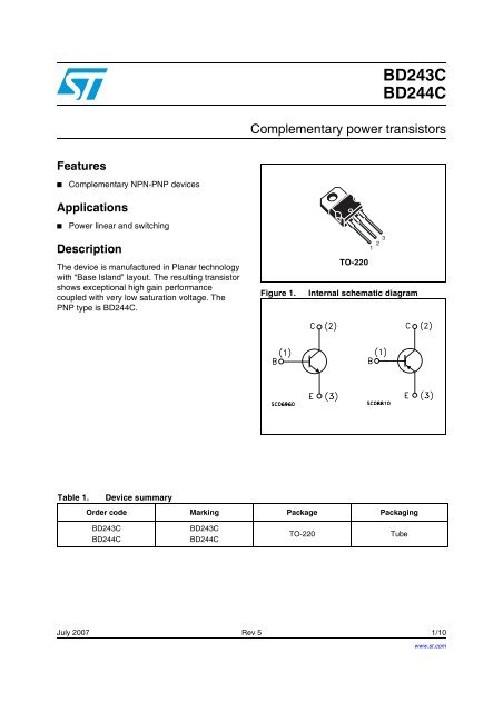
Figure 1.<br />
TO-220<br />
1 2 3<br />
Internal schematic diagram<br />
Table 1.<br />
Device summary<br />
Order code Marking Package Packaging<br />
BD243C<br />
BD244C<br />
BD243C<br />
BD244C<br />
TO-220<br />
Tube<br />
July 2007 Rev 5 1/10<br />
www.st.com<br />
10
Absolute maximum ratings<br />
BD243C BD244C<br />
1 Absolute maximum ratings<br />
Table 2.<br />
Absolute maximum ratings<br />
Symbol<br />
Parameter<br />
Value<br />
Unit<br />
BD243C (NPN)<br />
BD244C (PNP)<br />
V CBO Collector-base voltage (I E = 0) 100 V<br />
V CEO Collector-emitter voltage (I B = 0) 100 V<br />
V EBO Emitte-base voltage (I C = 0) 5 V<br />
I C Collector current 6 A<br />
I CM Collector peak current (t P < 5ms) 10 A<br />
I B Base current 2 A<br />
P TOT Total dissipation at T c = 25°C 65 W<br />
T stg Storage temperature -65 to 150 °C<br />
T J Max. operating junction temperature 150 °C<br />
Note:<br />
For PNP types voltage and current values are negative<br />
2/10
BD243C BD244C<br />
Electrical characteristics<br />
2 Electrical characteristics<br />
(T case = 25°C; unless otherwise specified)<br />
Table 3.<br />
Electrical characteristics<br />
Symbol Parameter Test Conditions Min. Typ. Max. Unit<br />
I CES<br />
I CEO<br />
I EBO<br />
V<br />
(1)<br />
CEO(sus)<br />
V<br />
(1)<br />
CE(sat)<br />
Collector cut-off current<br />
(V BE = 0)<br />
Collector cut-off current<br />
(I B = 0)<br />
Emitter cut-off current<br />
(I C = 0)<br />
Collector-emitter<br />
sustaining voltage (I B = 0)<br />
Collector-emitter<br />
saturation voltage<br />
V CE = 100V 0.4 mA<br />
V CE = 60V 0.7 mA<br />
V EB = 5V 1 mA<br />
I C = 30mA 100 V<br />
I C = 6A __ I B = 1A 1.5 V<br />
V BE<br />
(1) Base-emitter voltage I C = 6A _____ I B = 1A 2 V<br />
h FE<br />
(1)<br />
DC current gain<br />
I C = 0.3mA__<br />
I C = 3A _____<br />
V CE = 4V<br />
V CE = 4V<br />
30<br />
15<br />
1. Pulsed duration = 300 ms, duty cycle ≤ 2%.<br />
Note:<br />
For PNP types voltage and current values are negative.<br />
3/10
Electrical characteristics<br />
BD243C BD244C<br />
2.1 Typical characteristics<br />
Figure 2. Safe operating area Figure 3. Derating curve<br />
Figure 4. DC current gain (NPN) Figure 5. DC current gain (PNP)<br />
Figure 6.<br />
Collector-emitter saturation<br />
voltage (NPN)<br />
Figure 7.<br />
Collector-emitter saturation<br />
voltage (PNP)<br />
4/10
BD243C BD244C<br />
Electrical characteristics<br />
Figure 8.<br />
Base-emitter saturation<br />
voltage (NPN)<br />
Figure 9.<br />
Base-emitter saturation<br />
voltage (PNP)<br />
Figure 10.<br />
Base-emitter saturation<br />
voltage (NPN)<br />
Figure 11.<br />
Base-emitter saturation<br />
voltage (PNP)<br />
Figure 12. BT(ON) time (NPN) Figure 13. BT (ON) time (PNP)<br />
5/10
Electrical characteristics<br />
BD243C BD244C<br />
Figure 14.<br />
Resistive load switching time<br />
(NPN)<br />
Figure 15.<br />
Resistive load switching time<br />
(PNP)<br />
Figure 16.<br />
Resistive load switching time<br />
(NPN)<br />
Figure 17.<br />
Resistive load switching time<br />
(PNP)<br />
Figure 18.<br />
Collector-base and collectoremitter<br />
capacitance (NPN)<br />
Figure 19.<br />
Collector-base and collectoremitter<br />
capacitance (PNP)<br />
6/10
BD243C BD244C<br />
Package mechanical data<br />
3 Package mechanical data<br />
In order to meet environmental requirements, ST offers these devices in<br />
ECOPACK® packages. These packages have a Lead-free second level<br />
interconnect . The category of second level interconnect is marked on the<br />
package and on the inner box label, in compliance with JEDEC Standard JESD97.<br />
The maximum ratings related to soldering conditions are also marked on the inner<br />
box label. ECOPACK is an ST trademark. ECOPACK specifications are available<br />
at: www.st.com<br />
7/10
Package mechanical data<br />
BD243C BD244C<br />
TO-220 Mechanical data<br />
DIM.<br />
mm.<br />
MIN. TYP MAX.<br />
A 4.40 4.60<br />
b 0.61 0.88<br />
b1 1.14 1.70<br />
c 0.49 0.70<br />
D 15.25 15.75<br />
D1 1.27<br />
E 10 10.40<br />
e 2.40 2.70<br />
e1 4.95 5.15<br />
F 1.23 1.32<br />
H1 6.20 6.60<br />
J1 2.40 2.72<br />
L 13 14<br />
L1 3.50 3.93<br />
L20 16.40<br />
L30 28.90<br />
øP 3.75 3.85<br />
Q 2.65 2.95<br />
8/10
BD243C BD244C<br />
Revision history<br />
4 Revision history<br />
Table 4. Revision history<br />
Date Revision Changes<br />
13-Sep-2005 4 New datasheet according to MLD-PWR/05/1267<br />
25-Jul-2007 5<br />
Figures 2, 3, 4, 5, 6, 7, 8, 9, 10, 11, 12, 13, 14, 15, 16, 17, 18 and<br />
figure 19, added<br />
9/10
BD243C BD244C<br />
Please Read Carefully:<br />
Information in this document is provided solely in connection with ST products. <strong>STMicroelectronics</strong> NV and its subsidiaries (“ST”) reserve the<br />
right to make changes, corrections, modifications or improvements, to this document, and the products and services described herein at any<br />
time, without notice.<br />
All ST products are sold pursuant to ST’s terms and conditions of sale.<br />
Purchasers are solely responsible for the choice, selection and use of the ST products and services described herein, and ST assumes no<br />
liability whatsoever relating to the choice, selection or use of the ST products and services described herein.<br />
No license, express or implied, by estoppel or otherwise, to any intellectual property rights is granted under this document. If any part of this<br />
document refers to any third party products or services it shall not be deemed a license grant by ST for the use of such third party products<br />
or services, or any intellectual property contained therein or considered as a warranty covering the use in any manner whatsoever of such<br />
third party products or services or any intellectual property contained therein.<br />
UNLESS OTHERWISE SET FORTH IN ST’S TERMS AND CONDITIONS OF SALE ST DISCLAIMS ANY EXPRESS OR IMPLIED<br />
WARRANTY WITH RESPECT TO THE USE AND/OR SALE OF ST PRODUCTS INCLUDING WITHOUT LIMITATION IMPLIED<br />
WARRANTIES OF MERCHANTABILITY, FITNESS FOR A PARTICULAR PURPOSE (AND THEIR EQUIVALENTS UNDER THE LAWS<br />
OF ANY JURISDICTION), OR INFRINGEMENT OF ANY PATENT, COPYRIGHT OR OTHER INTELLECTUAL PROPERTY RIGHT.<br />
UNLESS EXPRESSLY APPROVED IN WRITING BY AN AUTHORIZED ST REPRESENTATIVE, ST PRODUCTS ARE NOT<br />
RECOMMENDED, AUTHORIZED OR WARRANTED FOR USE IN MILITARY, AIR CRAFT, SPACE, LIFE SAVING, OR LIFE SUSTAINING<br />
APPLICATIONS, NOR IN PRODUCTS OR SYSTEMS WHERE FAILURE OR MALFUNCTION MAY RESULT IN PERSONAL INJURY,<br />
DEATH, OR SEVERE PROPERTY OR ENVIRONMENTAL DAMAGE. ST PRODUCTS WHICH ARE NOT SPECIFIED AS "AUTOMOTIVE<br />
GRADE" MAY ONLY BE USED IN AUTOMOTIVE APPLICATIONS AT USER’S OWN RISK.<br />
Resale of ST products with provisions different from the statements and/or technical features set forth in this document shall immediately void<br />
any warranty granted by ST for the ST product or service described herein and shall not create or extend in any manner whatsoever, any<br />
liability of ST.<br />
ST and the ST logo are trademarks or registered trademarks of ST in various countries.<br />
Information in this document supersedes and replaces all information previously supplied.<br />
The ST logo is a registered trademark of <strong>STMicroelectronics</strong>. All other names are the property of their respective owners.<br />
© 2007 <strong>STMicroelectronics</strong> - All rights reserved<br />
<strong>STMicroelectronics</strong> group of companies<br />
Australia - Belgium - Brazil - Canada - China - Czech Republic - Finland - France - Germany - Hong Kong - India - Israel - Italy - Japan -<br />
Malaysia - Malta - Morocco - Singapore - Spain - Sweden - Switzerland - United Kingdom - United States of America<br />
www.st.com<br />
10/10


