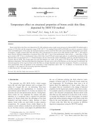
S.H. Jeong et al. / Surface & Coatings Technology 193 (2005) 340–344 343 Fig. 3. Optical transmittance <strong>of</strong> SZO films prepared (a) at RTwith different AgNO 3 contents in the target <strong>and</strong> (c) at different substrate temperatures with 4 wt.% SZO target. The <strong>optical</strong> b<strong>and</strong> gap <strong>of</strong> the SZO films (b) at RT with different AgNO 3 contents in the target; (d) at different substrate temperatures with 4 wt.% SZO target. their peak positions were very different from one metal <strong>oxide</strong> to another. Greatly, the 10 electrons in ZnO completely occupied both the 2t 2g , <strong>and</strong> 3e g orbitals, giving rise to the disappearance <strong>of</strong> any sharp features in the energy range b535 eV. The lowest unoccupied molecular orbital for ZnO was the 3a 1g orbital, which was most likely the origin for the broad O K-edge feature at 538 eV [21]. Fig. 5 shows the O K-edge features by the amount <strong>of</strong> the Ag dopant. Here, the O K-edge features <strong>of</strong> pure ZnO appeared broadly at 540 eV but disappeared under 535 eV. According to the amount <strong>of</strong> the Ag dopant, whole change was not observed greatly. When the MO theory is applied to several molecular orbitals, we say it is b<strong>and</strong>. In addition, occupied MO represents valence b<strong>and</strong>, <strong>and</strong> unoccupied MO represent Fig. 4. XP survey spectra <strong>of</strong> 4 wt.% SZO film after Ar sputtering. Table 1 The compositions <strong>of</strong> the SZO films prepared by rf magnetron sputtering Zn O Ag (1) Pure ZnO (RT) 51.48 48.52 (2) 2 wt.% SZO film (RT) 53.23 45.73 1.04 (3) 4 wt.% SZO film (RT) 52.70 45.36 1.94 (4) 4 wt.% SZO film (100 8C) 52.27 45.75 1.98 (5) 4 wt.% SZO film (200 8C) 60.75 37.14 2.11
344 S.H. Jeong et al. / Surface & Coatings Technology 193 (2005) 340–344 ion diffusion. When the SZO films were stoichiometric, the crystalllinity <strong>and</strong> the transmittance increased. The <strong>optical</strong> b<strong>and</strong> gap was narrowed with increasing Ag contents. This was expected because the change <strong>of</strong> valence b<strong>and</strong> produced by Ag–O due to the Ag + was substituted into the Zn + site. Acknowledgments Fig. 5. Oxygen K-edge near-edge X-ray absorption fine structure (NEXAFS) spectra measured from the SZO films with different AgNO 3 contents in the target at RT. conduction b<strong>and</strong>. Because the NEXAFS feature appears when the electron excites to unoccupied MO, we can say that it express many <strong>of</strong> information <strong>of</strong> conduction b<strong>and</strong>. In detail, the peak increased gradually about 543 eV caused by the increase <strong>of</strong> density <strong>of</strong> conduction b<strong>and</strong> by Ag doping. This was expected to peak which was caused by Ag–O created by the Ag dopant. NEXAFS was measured after Ar ion sputtering for 10 min to remove adsorbed species on the surface <strong>of</strong> the SZO film. 4. Conclusions Silver-<strong>doped</strong> ZnO (SZO) films with various Ag contents (0, 2, <strong>and</strong> 4 wt.%) were prepared by rf magnetron sputtering on glass substrates with extraordinarily designed ZnO target. The structural <strong>and</strong> <strong>optical</strong> <strong>properties</strong> <strong>of</strong> SZO films depended on coating parameter, such as dopant content, in target <strong>and</strong> substrate temperature. The <strong>sputtered</strong> SZO films have a preferred crystalline orientation <strong>of</strong> (002) direction. As amounts <strong>of</strong> the Ag dopant in the target were increased, the angles <strong>of</strong> (002) peaks were shifted to lower, indicating that the lattice parameter <strong>of</strong> SZO film was increased in the c-axis with increasing the amounts <strong>of</strong> the Ag dopant. Therefore, we can conclude that the big Ag ions (122 pm) were substituted into the Zn + (72 pm) site in the SZO crystal. As the amounts <strong>of</strong> the Ag dopant in the target were increased, the crystallinity <strong>and</strong> the transmittance were decreased, while the substrate temperature decreased. But the crystallinity <strong>and</strong> the transmittance <strong>of</strong> SZO films were decreased at 200 8C due to various <strong>of</strong> composition by Ag This work was supported by the BK21 project <strong>of</strong> the Ministry <strong>of</strong> Education Korea <strong>and</strong> by the Center for Advanced Plasma Surface Technology as well as CNNC at the Sungkyunkwan University. The NEXAFS experiments at Pohang Accelerator Laboratory (PLS) were supported in part by the Korean Ministry Of Science <strong>and</strong> Technology (MOST) <strong>and</strong> Pohang University <strong>of</strong> Science <strong>and</strong> Technology (POSTECH). References [1] K.C. Park, D.Y. Ma, K.H. Kim, Thin Solid Films 305 (1997) 201. [2] J. Ma, J. Feng, D.-H. Zhang, H.-L. Ma, S.-Y. Li, Thin Solid Films 357 (1999) 98. [3] S.H. Jeong, J.W. Lee, S.B. Lee, J.-H. Boo, Thin Solid Films 435 (2003) 78. [4] S.H. Jeong, S. Kho, D. Jung, S.B. Lee, J.-H. Boo, Surf. Coat. Technol. 174 (2003) 187. [5] J.B. Lee, H.J. Kim, S.G. Kim, C.S. Hwang, S.-H. Hong, Y.H. Shin, N.H. Lee, Thin Solid Films 435 (2003) 179. [6] Y. Yoshino, T. Makino, Y. Katayama, T. Hata, Vacuum 59 (2000) 538. [7] J.F. Chang, H.H. Kuo, I.C. Leu, M.H. Hon, Sens. Actuators, B, Chem. 84 (2002) 258. [8] D.H. Zhang, T.L. Yang, J. Ma, Appl. Surf. Sci. 158 (2000) 43. [9] W.S. Lan, S.J. Fonash, J. Electron. Mater. 16 (1987) 141. [10] K. Ellmer, R. Wendt, Surf. Coat. Technol. 93 (1997) 21. [11] T. Schuler, M.A. Aegerter, Thin Solid Films 351 (1999) 125. [12] J.L. Deschanvres, B. Bochu, J.C. Joubert, J. Phys. 4 (3) (1993) 485. [13] H. Kim, A. Pique, J.S. Horwitz, H. Murata, Z.H. Kafafi, C.M. Gilmore, D.B. Chrisey, Thin Solid Films 377 (2000) 798. [14] F.-J. Haug, Z.S. Geller, H. Zogg, A.N. Tiwari, C. Vignali, J. Vac. Sci. Technol., A 19 (2001) 171. [15] P. Nunes, E. Fortunato, R. Martins, Thin Solid Films 383 (2001) 277. [16] T. Minami, T. Yamamoto, T. Miyata, Thin Solid Films 366 (2000) 63. [17] K. Postava, H. Sueki, M. Aoyama, T. Yamaguchi, K. Murakami, Y. Igasasi, Appl. Surf. Sci. 175 (2001) 543. [18] J. Han, P.Q. Mantas, A.M.R. Senos, J. Eur. Ceram. Soc. 21 (2001) 1883. [19] J. Fan, R. Freer, J. Appl. Phys. 77 (1995) 4795. [20] C.A.K. Gouvea, F. Wypych, S.G. Moraes, N. Duran, P. Peralta- Zamora, Chemosphere 40 (2000) 427. [21] J.G. Chen, B. Fruhberger, M.L. Colaianni, J. Vac. Sci. Technol., A 14 (1996) 1668. [22] L.A. Grunes, R.D. Leapman, C.N. Wilker, R. H<strong>of</strong>fman, A.B. Kunz, Phys. Rev., B 25 (1982) 7157.