Structural and optical properties of silver-doped zinc oxide sputtered ...
Structural and optical properties of silver-doped zinc oxide sputtered ...
Structural and optical properties of silver-doped zinc oxide sputtered ...

Create successful ePaper yourself
Turn your PDF publications into a flip-book with our unique Google optimized e-Paper software.
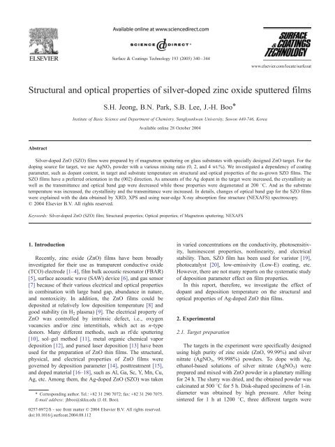
Surface & Coatings Technology 193 (2005) 340–344<br />
www.elsevier.com/locate/surfcoat<br />
<strong>Structural</strong> <strong>and</strong> <strong>optical</strong> <strong>properties</strong> <strong>of</strong> <strong>silver</strong>-<strong>doped</strong> <strong>zinc</strong> <strong>oxide</strong> <strong>sputtered</strong> films<br />
S.H. Jeong, B.N. Park, S.B. Lee, J.-H. Boo*<br />
Institute <strong>of</strong> Basic Science <strong>and</strong> Department <strong>of</strong> Chemistry, Sungkyunkwan University, Suwon 440-746, Korea<br />
Available online 28 October 2004<br />
Abstract<br />
Silver-<strong>doped</strong> ZnO (SZO) films were prepared by rf magnetron sputtering on glass substrates with specially designed ZnO target. For the<br />
doping source for target, we use AgNO 3 powder with a various mixing ratio (0, 2, <strong>and</strong> 4 wt.%). We investigated a dependency <strong>of</strong> coating<br />
parameter, such as dopant content, in target <strong>and</strong> substrate temperature on structural <strong>and</strong> <strong>optical</strong> <strong>properties</strong> <strong>of</strong> the as-grown SZO films. The<br />
SZO films have a preferred orientation in the (002) direction. As amounts <strong>of</strong> the Ag dopant in the target were increased, the crystallinity as<br />
well as the transmittance <strong>and</strong> <strong>optical</strong> b<strong>and</strong> gap were decreased while those <strong>properties</strong> were degenerated at 200 8C. And as the substrate<br />
temperature was increased, the crystallinity <strong>and</strong> the transmittance were increased. In details, changes <strong>of</strong> <strong>optical</strong> b<strong>and</strong> gap for the SZO films<br />
were explained with the data obtained by XRD, XPS <strong>and</strong> using near-edge X-ray absorption fine structure (NEXAFS) spectroscopy.<br />
D 2004 Elsevier B.V. All rights reserved.<br />
Keywords: Silver-<strong>doped</strong> ZnO (SZO) film; <strong>Structural</strong> <strong>properties</strong>; Optical <strong>properties</strong>; rf Magnetron sputtering; NEXAFS<br />
1. Introduction<br />
Recently, <strong>zinc</strong> <strong>oxide</strong> (ZnO) films have been broadly<br />
investigated for their use as transparent conductive <strong>oxide</strong><br />
(TCO) electrode [1–4], film bulk acoustic resonator (FBAR)<br />
[5], surface acoustic wave (SAW) device [6], <strong>and</strong> gas sensor<br />
[7] because <strong>of</strong> their various electrical <strong>and</strong> <strong>optical</strong> <strong>properties</strong><br />
in combination with large b<strong>and</strong> gap, abundance in nature,<br />
<strong>and</strong> nontoxicity. In addition, the ZnO films could be<br />
deposited at relatively low deposition temperature [8] <strong>and</strong><br />
good stability (in H 2 plasma) [9]. The electrical property <strong>of</strong><br />
ZnO was controlled by intrinsic defect, i.e., oxygen<br />
vacancies <strong>and</strong>/or <strong>zinc</strong> interstitials, which act as n-type<br />
donors. Many different methods, such as rf/dc sputtering<br />
[10], sol–gel method [11], metal organic chemical vapor<br />
deposition [12], <strong>and</strong> pursed laser deposition [13] have been<br />
used for the preparation <strong>of</strong> ZnO thin films. The structural,<br />
physical, <strong>and</strong> electrical <strong>properties</strong> <strong>of</strong> ZnO films were<br />
governed by deposition parameter [14], posttreatment [15],<br />
<strong>and</strong> <strong>doped</strong> material [16–18], such as Al, Ga, Sc, Y, Mn, Cu,<br />
Ag, etc. Among them, the Ag-<strong>doped</strong> ZnO (SZO) was taken<br />
* Corresponding author. Tel.: +82 31 290 7072; fax: +82 31 290 7075.<br />
E-mail address: jhboo@skku.edu (J.-H. Boo).<br />
in varied concentrations on the conductivity, photosensitivity,<br />
luminescent <strong>properties</strong>, nonlinearity, <strong>and</strong> electrical<br />
stability. Then, SZO film has been used for varistor [19],<br />
photocatalyst [20], low-emissivity (Low-E) coating, etc.<br />
However, there are not many reports on the systematic study<br />
<strong>of</strong> deposition parameter effect on film <strong>properties</strong>.<br />
In this report, therefore, we investigate the effect <strong>of</strong><br />
dopant <strong>and</strong> deposition temperature on the structural <strong>and</strong><br />
<strong>optical</strong> <strong>properties</strong> <strong>of</strong> Ag-<strong>doped</strong> ZnO thin films.<br />
2. Experimental<br />
2.1. Target preparation<br />
The targets in the experiment were specifically designed<br />
using high purity <strong>of</strong> <strong>zinc</strong> <strong>oxide</strong> (ZnO, 99.99%) <strong>and</strong> <strong>silver</strong><br />
nitrate (AgNO 3 , 99.998%) powders. To dope with Ag,<br />
ethanol-based solutions <strong>of</strong> <strong>silver</strong> nitrate (AgNO 3 ) were<br />
prepared <strong>and</strong> mixed with ZnO powder in a planetary milling<br />
for 24 h. The slurry was dried, <strong>and</strong> the obtained powder was<br />
calcinated at 500 8C for 5 h. Disk-shaped specimens <strong>of</strong> 1-in.<br />
diameter was obtained by high pressure. After being<br />
sintered for 1 h at 1200 8C, three different targets were<br />
0257-8972/$ - see front matter D 2004 Elsevier B.V. All rights reserved.<br />
doi:10.1016/j.surfcoat.2004.08.112
S.H. Jeong et al. / Surface & Coatings Technology 193 (2005) 340–344 341<br />
prepared with different weight percent (wt.%) <strong>of</strong> AgNO 3 in<br />
the targets: pure ZnO, 2 wt.% SZO, <strong>and</strong> 4 wt.% SZO.<br />
2.2. Deposition conditions<br />
The sputtering system was pumped down to 310 6<br />
Torr using turbo molecular pump. The working pressure<br />
which mainly consisted <strong>of</strong> a high-purity Ar(99.99%) gas<br />
was 32 mTorr. The glass substrates were cleaned in an<br />
ultrasonic cleaner for 10 min with acetone, alcohol, alkaline<br />
solution <strong>and</strong> then distilled water. All substrates were blown<br />
with dry nitrogen gas. ZnO films were deposited on the<br />
substrates at room temperature (RT) with rf power <strong>of</strong> 150 W<br />
after presputtering <strong>of</strong> the targets with Ar plasma for 5 min.<br />
Due to the practical applicability <strong>of</strong> SZO films, 150- to 200-<br />
nm-thick samples were typically prepared for <strong>optical</strong><br />
measurements. The crystal structure, microstructure, <strong>and</strong><br />
the thickness were observed using X-ray diffraction (XRD)<br />
<strong>and</strong> scanning electron microscope (SEM), respectively. X-<br />
ray photoelectron spectroscopy (XPS) was also utilized to<br />
analyze the chemical state <strong>of</strong> SZO films. The <strong>optical</strong><br />
transmittance measurements were performed with a UV/<br />
visible spectrophotometer. The oxygen K-edge features <strong>of</strong><br />
SZO films were also investigated using near-edge X-ray<br />
absorption fine structure (NEXAFS) spectroscopy.<br />
3. Results <strong>and</strong> discussion<br />
3.1. <strong>Structural</strong> characterization<br />
We investigated how the growth rate was related to<br />
deposition parameters, such as substrate temperature, target<br />
to substrate distance (D ts ), rf power, etc. Details <strong>of</strong> the ZnO<br />
growth have already been described in our previous papers<br />
[3,4].<br />
Fig. 1(a) shows the XRD patterns obtained from 150-nmthick<br />
SZO films prepared with different sputtering targets at<br />
room temperature <strong>and</strong> 150 W. As shown in Fig. 1(a), only<br />
the (002) diffraction peak is observed at 2h=33.6–34.308,<br />
indicating that all <strong>of</strong> the obtained films had a preferred<br />
orientation with the c-axis perpendicular to the substrate. In<br />
addition, the peaks position <strong>of</strong> the (002) plane was also<br />
shifted to lower 2h values with increasing amounts <strong>of</strong> Ag<br />
content. The reason is that the lattice parameter <strong>of</strong> SZO was<br />
increased in the c-axis with increasing Ag dopant. In<br />
previous works, Park et al. [1] reported that the small Al<br />
ions (53 pm) was substituted into the Zn + (72 pm) site in the<br />
Al-<strong>doped</strong> ZnO crystal. Therefore, the 2h values <strong>of</strong> the (002)<br />
plane increased because crystal size decreased. Conclusively<br />
we can conclude that that the big Ag ions (122 pm) were<br />
substituted into the Zn + (72 pm) in the SZO crystal.<br />
Moreover, the intensity <strong>of</strong> (002) peaks gradually decreased<br />
<strong>and</strong> broadened according to increasing Ag dopant. Not only<br />
the full width half maximums (FWHMs) but also the<br />
intensity <strong>of</strong> the peaks were carried out to evaluate the<br />
Fig. 1. The XRD patterns <strong>of</strong> SZO films were deposited on glass substrate.<br />
The high-resolution XRD patterns with 0, 2, <strong>and</strong> 4 wt.% AgNO 3 contents in<br />
the target at RT(a) <strong>and</strong> at different substrate temperatures with 4 wt.% SZO<br />
target (b).<br />
crystalline quality <strong>of</strong> the films. As a result, the FWHMs <strong>of</strong><br />
the (002) peaks decreased with increasing Ag dopant (0.288,<br />
0.408, <strong>and</strong> 0.618, respectively). The reason is that the<br />
crystallinity decreased with increasing Ag dopant in SZO<br />
films because <strong>of</strong> the Ag + substituted into Zn + site.<br />
Fig. 1(b) shows that the XRD spectra for SZO films were<br />
prepared on glass with 4 wt.% SZO target from room<br />
temperature to 200 8C. In these results, the intensity <strong>of</strong> the<br />
(002) peaks increased with increasing substrate temperature<br />
at 100 8C. However, the intensity <strong>of</strong> the (002) peak<br />
decreased at 200 8C. At this time, the FWHMs <strong>of</strong> the<br />
(002) peaks were not changed (about 0.438). This is caused<br />
by the crystallinity <strong>of</strong> the deposited films which improved<br />
with increasing substrate temperature at b100 8C. But the<br />
crystallinity <strong>of</strong> SZO film was retrograde at 250 8C.<br />
SEM micrograph analysis (Fig. 2) indicated the granular<br />
character <strong>of</strong> the deposited films. The average grain size<br />
measured from these micrographs was in the range <strong>of</strong> 25–40<br />
nm. This result did not relate to the amount <strong>of</strong> Ag dopant.
342<br />
S.H. Jeong et al. / Surface & Coatings Technology 193 (2005) 340–344<br />
content. With Ag content increasing, the absorption edge<br />
slightly shifted to a longer wavelength region [Fig. 3(a)].<br />
However, the result <strong>of</strong> Fig. 3(c) shows the average transmittance<br />
was decreased with increasing the T sub (from 80 to<br />
50%). The reason is that the metallic property grown (to<br />
illustrate following XPS analysis) in SZO film with<br />
T sub =200 8C.<br />
The <strong>optical</strong> gap (Eg) <strong>of</strong> the SZO film can be obtained by<br />
plotting a 2 vs. hm (a is the absorption coefficient <strong>and</strong> hm is<br />
the photon energy) <strong>and</strong> extrapolating the straight-line<br />
portion <strong>of</strong> this plot to the photon energy axis [1]. Fig.<br />
3(b) shows the variation <strong>of</strong> <strong>optical</strong> b<strong>and</strong> gap as a function <strong>of</strong><br />
Ag contents. It showed that a b<strong>and</strong> gap narrowing down<br />
with increasing Ag contents. The reason is that the Ag + was<br />
substituted into the Zn + . However, Eg change by varying<br />
temperatures could not be observed in Fig. 3(d).<br />
3.3. Chemical state on the surface<br />
Fig. 3(b) shows that XP survey spectra obtained after Ar<br />
sputtering for an SZO film was prepared at RT with 4 wt.%<br />
AgNO 3 -<strong>doped</strong> ZnO target. Zinc, oxygen <strong>and</strong> Ag peaks are<br />
observed, <strong>and</strong> there was no contamination except for carbon<br />
[Fig. 4(a)].<br />
With high-resolution XPS spectra <strong>of</strong> Zn 2p 3/2 , O 1s, <strong>and</strong><br />
Ag 3d considering their atomic sensitivity, one could get the<br />
formation in the SZO film (see Table 1). Table 1 shows the<br />
percentages <strong>of</strong> <strong>silver</strong> became 0, 1.04, <strong>and</strong> 1.94 in the SZO<br />
films as dopant increased from 0 to 4 wt.%. It was certified<br />
that it is due to dopant increase that 2üÇ shifted by low<br />
angle in the XRD result. In addition, when increasing the<br />
substrate temperature, it was observed that crystallinity <strong>and</strong><br />
transmittance increased until 100 8C. These became the ZnO<br />
ratio to stoichiometry in the SZO films. We can observe that<br />
ZnO films became stoichometry as substrate temperature<br />
increased in Table 1. However, deposition at 200 8C<br />
dropped crystallinity <strong>and</strong> transmittance. These were caused<br />
by metallic character grown in the SZO film. We can<br />
observe that the quantity <strong>of</strong> <strong>zinc</strong> greatly increased in the<br />
SZO film in Table 1(5).<br />
3.4. Oxygen K-edge features <strong>of</strong> SZO films<br />
Fig. 2. The SEM images <strong>of</strong> the SZO films were prepared with different<br />
AgNO 3 content in the target. (a) Pure ZnO, (b) 2 wt.% SZO film, <strong>and</strong> (c) 4<br />
wt.% SZO films.<br />
3.2. Optical <strong>properties</strong><br />
We measured that the average transmittance in the visible<br />
range was from 90% to 85% with the increase <strong>of</strong> the Ag<br />
Chen et al. [21] reported a comparison <strong>of</strong> oxygen K-edge<br />
NEXAFS spectra <strong>of</strong> several 3d transition metal <strong>oxide</strong>s with<br />
the different number <strong>of</strong> d-electron (TiO 2 -d 0 , CrO 3 -d 3 ,FeOd<br />
6 , NiO-d 8 , <strong>and</strong> ZnO-d 10 , etc.). Here, the O K-edges had<br />
four features. The four O K-edge features could be assigned<br />
to the one-electron transition from the O 1s orbital to the<br />
2t 2g , 3e g , 3a 1g , <strong>and</strong> 4t 1u orbitals <strong>of</strong> TiO 2 , respectively.<br />
Grunes et al. [22] reported that this assignment was in<br />
essential agreement with a tight-binding extended Huckel<br />
b<strong>and</strong> structure calculation. The simple one-electron excitation<br />
scheme could be used to explain the qualitative<br />
differences in the transitions to the two molecular orbitals<br />
(2t g <strong>and</strong> 3e g ). Then, the number <strong>of</strong> O K-edge features <strong>and</strong>
S.H. Jeong et al. / Surface & Coatings Technology 193 (2005) 340–344 343<br />
Fig. 3. Optical transmittance <strong>of</strong> SZO films prepared (a) at RTwith different AgNO 3 contents in the target <strong>and</strong> (c) at different substrate temperatures with 4 wt.% SZO<br />
target. The <strong>optical</strong> b<strong>and</strong> gap <strong>of</strong> the SZO films (b) at RT with different AgNO 3 contents in the target; (d) at different substrate temperatures with 4 wt.% SZO target.<br />
their peak positions were very different from one metal<br />
<strong>oxide</strong> to another. Greatly, the 10 electrons in ZnO<br />
completely occupied both the 2t 2g , <strong>and</strong> 3e g orbitals, giving<br />
rise to the disappearance <strong>of</strong> any sharp features in the energy<br />
range b535 eV. The lowest unoccupied molecular orbital for<br />
ZnO was the 3a 1g orbital, which was most likely the origin<br />
for the broad O K-edge feature at 538 eV [21]. Fig. 5 shows<br />
the O K-edge features by the amount <strong>of</strong> the Ag dopant.<br />
Here, the O K-edge features <strong>of</strong> pure ZnO appeared broadly<br />
at 540 eV but disappeared under 535 eV. According to the<br />
amount <strong>of</strong> the Ag dopant, whole change was not observed<br />
greatly. When the MO theory is applied to several molecular<br />
orbitals, we say it is b<strong>and</strong>. In addition, occupied MO<br />
represents valence b<strong>and</strong>, <strong>and</strong> unoccupied MO represent<br />
Fig. 4. XP survey spectra <strong>of</strong> 4 wt.% SZO film after Ar sputtering.<br />
Table 1<br />
The compositions <strong>of</strong> the SZO films prepared by rf magnetron sputtering<br />
Zn O Ag<br />
(1) Pure ZnO (RT) 51.48 48.52<br />
(2) 2 wt.% SZO film (RT) 53.23 45.73 1.04<br />
(3) 4 wt.% SZO film (RT) 52.70 45.36 1.94<br />
(4) 4 wt.% SZO film (100 8C) 52.27 45.75 1.98<br />
(5) 4 wt.% SZO film (200 8C) 60.75 37.14 2.11
344<br />
S.H. Jeong et al. / Surface & Coatings Technology 193 (2005) 340–344<br />
ion diffusion. When the SZO films were stoichiometric, the<br />
crystalllinity <strong>and</strong> the transmittance increased. The <strong>optical</strong><br />
b<strong>and</strong> gap was narrowed with increasing Ag contents. This<br />
was expected because the change <strong>of</strong> valence b<strong>and</strong> produced<br />
by Ag–O due to the Ag + was substituted into the Zn + site.<br />
Acknowledgments<br />
Fig. 5. Oxygen K-edge near-edge X-ray absorption fine structure<br />
(NEXAFS) spectra measured from the SZO films with different AgNO 3<br />
contents in the target at RT.<br />
conduction b<strong>and</strong>. Because the NEXAFS feature appears<br />
when the electron excites to unoccupied MO, we can say<br />
that it express many <strong>of</strong> information <strong>of</strong> conduction b<strong>and</strong>. In<br />
detail, the peak increased gradually about 543 eV caused by<br />
the increase <strong>of</strong> density <strong>of</strong> conduction b<strong>and</strong> by Ag doping.<br />
This was expected to peak which was caused by Ag–O<br />
created by the Ag dopant. NEXAFS was measured after Ar<br />
ion sputtering for 10 min to remove adsorbed species on the<br />
surface <strong>of</strong> the SZO film.<br />
4. Conclusions<br />
Silver-<strong>doped</strong> ZnO (SZO) films with various Ag contents<br />
(0, 2, <strong>and</strong> 4 wt.%) were prepared by rf magnetron sputtering<br />
on glass substrates with extraordinarily designed ZnO<br />
target. The structural <strong>and</strong> <strong>optical</strong> <strong>properties</strong> <strong>of</strong> SZO films<br />
depended on coating parameter, such as dopant content, in<br />
target <strong>and</strong> substrate temperature. The <strong>sputtered</strong> SZO films<br />
have a preferred crystalline orientation <strong>of</strong> (002) direction.<br />
As amounts <strong>of</strong> the Ag dopant in the target were increased,<br />
the angles <strong>of</strong> (002) peaks were shifted to lower, indicating<br />
that the lattice parameter <strong>of</strong> SZO film was increased in the<br />
c-axis with increasing the amounts <strong>of</strong> the Ag dopant.<br />
Therefore, we can conclude that the big Ag ions (122 pm)<br />
were substituted into the Zn + (72 pm) site in the SZO<br />
crystal. As the amounts <strong>of</strong> the Ag dopant in the target were<br />
increased, the crystallinity <strong>and</strong> the transmittance were<br />
decreased, while the substrate temperature decreased. But<br />
the crystallinity <strong>and</strong> the transmittance <strong>of</strong> SZO films were<br />
decreased at 200 8C due to various <strong>of</strong> composition by Ag<br />
This work was supported by the BK21 project <strong>of</strong> the<br />
Ministry <strong>of</strong> Education Korea <strong>and</strong> by the Center for<br />
Advanced Plasma Surface Technology as well as CNNC<br />
at the Sungkyunkwan University. The NEXAFS experiments<br />
at Pohang Accelerator Laboratory (PLS) were<br />
supported in part by the Korean Ministry Of Science <strong>and</strong><br />
Technology (MOST) <strong>and</strong> Pohang University <strong>of</strong> Science <strong>and</strong><br />
Technology (POSTECH).<br />
References<br />
[1] K.C. Park, D.Y. Ma, K.H. Kim, Thin Solid Films 305 (1997) 201.<br />
[2] J. Ma, J. Feng, D.-H. Zhang, H.-L. Ma, S.-Y. Li, Thin Solid Films 357<br />
(1999) 98.<br />
[3] S.H. Jeong, J.W. Lee, S.B. Lee, J.-H. Boo, Thin Solid Films 435<br />
(2003) 78.<br />
[4] S.H. Jeong, S. Kho, D. Jung, S.B. Lee, J.-H. Boo, Surf. Coat. Technol.<br />
174 (2003) 187.<br />
[5] J.B. Lee, H.J. Kim, S.G. Kim, C.S. Hwang, S.-H. Hong, Y.H. Shin,<br />
N.H. Lee, Thin Solid Films 435 (2003) 179.<br />
[6] Y. Yoshino, T. Makino, Y. Katayama, T. Hata, Vacuum 59 (2000) 538.<br />
[7] J.F. Chang, H.H. Kuo, I.C. Leu, M.H. Hon, Sens. Actuators, B, Chem.<br />
84 (2002) 258.<br />
[8] D.H. Zhang, T.L. Yang, J. Ma, Appl. Surf. Sci. 158 (2000) 43.<br />
[9] W.S. Lan, S.J. Fonash, J. Electron. Mater. 16 (1987) 141.<br />
[10] K. Ellmer, R. Wendt, Surf. Coat. Technol. 93 (1997) 21.<br />
[11] T. Schuler, M.A. Aegerter, Thin Solid Films 351 (1999) 125.<br />
[12] J.L. Deschanvres, B. Bochu, J.C. Joubert, J. Phys. 4 (3) (1993) 485.<br />
[13] H. Kim, A. Pique, J.S. Horwitz, H. Murata, Z.H. Kafafi, C.M.<br />
Gilmore, D.B. Chrisey, Thin Solid Films 377 (2000) 798.<br />
[14] F.-J. Haug, Z.S. Geller, H. Zogg, A.N. Tiwari, C. Vignali, J. Vac. Sci.<br />
Technol., A 19 (2001) 171.<br />
[15] P. Nunes, E. Fortunato, R. Martins, Thin Solid Films 383 (2001) 277.<br />
[16] T. Minami, T. Yamamoto, T. Miyata, Thin Solid Films 366 (2000) 63.<br />
[17] K. Postava, H. Sueki, M. Aoyama, T. Yamaguchi, K. Murakami, Y.<br />
Igasasi, Appl. Surf. Sci. 175 (2001) 543.<br />
[18] J. Han, P.Q. Mantas, A.M.R. Senos, J. Eur. Ceram. Soc. 21 (2001)<br />
1883.<br />
[19] J. Fan, R. Freer, J. Appl. Phys. 77 (1995) 4795.<br />
[20] C.A.K. Gouvea, F. Wypych, S.G. Moraes, N. Duran, P. Peralta-<br />
Zamora, Chemosphere 40 (2000) 427.<br />
[21] J.G. Chen, B. Fruhberger, M.L. Colaianni, J. Vac. Sci. Technol., A 14<br />
(1996) 1668.<br />
[22] L.A. Grunes, R.D. Leapman, C.N. Wilker, R. H<strong>of</strong>fman, A.B. Kunz,<br />
Phys. Rev., B 25 (1982) 7157.